Embed Size (px)
Citation preview

13
For price, delivery and to place orders: Hittite Microwave Corporation, 20 Alpha Road, Chelmsford, MA 01824Phone: 978-250-3343 Fax: 978-250-3373 Order On-line at www.hittite.com
Application Support: Phone: 978-250-3343 or [email protected] - 1
Ph
as
e s
hif
te
rs
- a
Na
LOG
- s
Mt
HMC931LP4E410° AnAlog PhAse shifter,
8 - 12 ghz
v02.0311
general Description
features
functional Diagram
the hMC931LP4e is an analog Phase shifter which is controlled via an analog control voltage from 0 to +13V. the hMC931LP4e provides a continuously variable phase shift of 0 to 410 degrees from 8 to 12 Ghz, with extremely consistent low insertion loss versus phase shift and frequency. the high accuracy hMC931LP4e is monotonic with respect to control voltage and features a typical low phase error of +12 / -7 degrees over a wide bandwidth. the hMC931LP4e is housed in an rohs compliant 4x4 mm QfN leadless package.
Wide Bandwidth: 8 - 12 Ghz
410° Phase shift
Low insertion Loss: 3.5 dB
Low Phase error: +12 / -7 deg typ.
single Positive Voltage Control
24 Lead 4x4 mm QfN Package: 16 mm²
electrical specifications, tA = +25° C, 50 ohm system
typical Applicationsthe hMC931LP4e is ideal for:
• eW receivers
• Military radar
• test equipment
• satellite Communications
• Beam forming Modules
Parameter Min. typ. Max. Units
frequency range 8 12 Ghz
Phase shift range 410 deg
insertion Loss 3.5 dB
return Loss (input and output) 12 dB
Control Voltage range 0 13 V
Control Current range ± 1 ma
input iP3 32 dBm
input Power @ - 5° shift in insertion Phase (Vctl = 0V) 11.2 dBm
input Power @ - 2° shift in insertion Phase (Vctl = 0.5V) 12 dBm
Phase Voltage sensitivity 32 deg/V
Phase error (peak) * +15 / -7 deg
Phase error (average) * +12 / -1 deg
Modulation Bandwidth 50 Mhz
insertion Phase temperature sensitivity 0.12 deg/°C
* Up to a phase shift range of 360 degrees.
OBSOLETE
Information furnished by Analog Devices is believed to be accurate and reliable. However, no responsibility is assumed by Analog Devices for its use, nor for any infringements of patents or other rights of third parties that may result from its use. Specifications subject to change without notice. No license is granted by implication or otherwise under any patent or patent rights of Analog Devices. Trademarks and registered trademarks are the property of their respective owners.
For price, delivery, and to place orders: Analog Devices, Inc., One Technology Way, P.O. Box 9106, Norwood, MA 02062-9106 Phone: 781-329-4700 • Order online at www.analog.com Application Support: Phone: 1-800-ANALOG-D

13
For price, delivery and to place orders: Hittite Microwave Corporation, 20 Alpha Road, Chelmsford, MA 01824Phone: 978-250-3343 Fax: 978-250-3373 Order On-line at www.hittite.com
Application Support: Phone: 978-250-3343 or [email protected]
Ph
as
e s
hif
te
rs
- a
Na
LOG
- s
Mt
13 - 2
HMC931LP4Ev02.0311
410° AnAlog PhAse shifter,8 - 12 ghz
Phase shift vs. Vctl
insertion loss vs. frequency
Phase shift vs. frequency @ Vctl = 6V (relative to Vctl = 0V)
insertion loss vs. Vctl , f = 10 ghz
Phase shift vs. frequency(relative to Vctl = 0V) Vctl = 0.5 to 13V
Phase error vs. frequency, fmean = 10 ghz [1]
[1] 0 to 10V provides 0 - 360 degrees phase shift range
-8
-7
-6
-5
-4
-3
-2
7 8 9 10 11 12 13
0V0.5V3V
6V9V13V
INS
ER
TIO
N L
OS
S (
dB)
FREQUENCY (GHz)
0
45
90
135
180
225
270
315
360
405
450
0 1 2 3 4 5 6 7 8 9 10 11 12 13
8 GHz10 GHz12 GHz
NO
RM
ALI
ZE
D P
HA
SE
SH
IFT
(de
gree
s)
Vctl (Vdc)
0
45
90
135
180
225
270
315
360
405
450
7 8 9 10 11 12 13
NO
RM
ALI
ZE
D P
HA
SE
SH
IFT
(de
gree
s)
FREQUENCY (GHz)
-6
-5
-4
-3
-2
-1
0
0 1 2 3 4 5 6 7 8 9 10 11 12 13
+ 25C+ 85C- 40C
INS
ER
TIO
N L
OS
S (
dB)
Vctl (Vdc)
230
240
250
260
270
280
290
300
310
320
330
7 8 9 10 11 12 13
+ 25C+ 85C- 40C
NO
RM
ALI
ZE
D P
HA
SE
SH
IFT
(de
gree
s)
FREQUENCY (GHz)
-20
-15
-10
-5
0
5
10
15
20
8 8.5 9 9.5 10 10.5 11 11.5 12
0.5V2V4V6V
8V10VAverage
PH
AS
E E
RR
OR
(de
gree
s)
FREQUENCY (GHz)
OBSOLETE
Information furnished by Analog Devices is believed to be accurate and reliable. However, no responsibility is assumed by Analog Devices for its use, nor for any infringements of patents or other rights of third parties that may result from its use. Specifications subject to change without notice. No license is granted by implication or otherwise under any patent or patent rights of Analog Devices. Trademarks and registered trademarks are the property of their respective owners.
For price, delivery, and to place orders: Analog Devices, Inc., One Technology Way, P.O. Box 9106, Norwood, MA 02062-9106 Phone: 781-329-4700 • Order online at www.analog.com Application Support: Phone: 1-800-ANALOG-D

13
For price, delivery and to place orders: Hittite Microwave Corporation, 20 Alpha Road, Chelmsford, MA 01824Phone: 978-250-3343 Fax: 978-250-3373 Order On-line at www.hittite.com
Application Support: Phone: 978-250-3343 or [email protected] - 3
Ph
as
e s
hif
te
rs
- a
Na
LOG
- s
Mt
HMC931LP4Ev02.0311
410° AnAlog PhAse shifter,8 - 12 ghz
input iP3 vs. Vctl, f = 10 ghz
insertion loss vs. Pin @ 10 ghz
insertion loss vs. Pin @ 8 ghz
second harmonics vs. Vctl, f = 10 ghz third harmonics vs. Vctl, f = 10 ghz
insertion loss vs. Pin @ 12 ghz
0
10
20
30
40
50
0 1 2 3 4 5 6 7 8 9 10 11 12 13
- 10 dBm0 dBm + 10 dBm
2ND
HA
RM
ON
IC (
dBc)
Vctl (Vdc)
15
20
25
30
35
40
0 1 2 3 4 5 6 7 8 9 10 11 12 13
- 10 dBm0 dBm+ 10 dBm
IP3
(dB
m)
Vctl (Vdc)
-7
-6
-5
-4
-3
-2
-10 -8 -6 -4 -2 0 2 4 6 8 10 12
0V0.5V6V13V
INS
ER
TIO
N L
OS
S (
dB)
INPUT POWER (dBm)
0
10
20
30
40
50
60
70
0 1 2 3 4 5 6 7 8 9 10 11 12 13
- 10 dBm0 dBm + 10 dBm
2ND
HA
RM
ON
IC (
dBc)
Vctl (Vdc)
-6
-5
-4
-3
-2
-10 -8 -6 -4 -2 0 2 4 6 8 10 12
0V0.5V6V13V
INS
ER
TIO
N L
OS
S (
dB)
INPUT POWER (dBm)
-7
-6
-5
-4
-3
-2
-10 -8 -6 -4 -2 0 2 4 6 8 10 12
0V0.5V6V13V
INS
ER
TIO
N L
OS
S (
dB)
INPUT POWER (dBm)
OBSOLETE
Information furnished by Analog Devices is believed to be accurate and reliable. However, no responsibility is assumed by Analog Devices for its use, nor for any infringements of patents or other rights of third parties that may result from its use. Specifications subject to change without notice. No license is granted by implication or otherwise under any patent or patent rights of Analog Devices. Trademarks and registered trademarks are the property of their respective owners.
For price, delivery, and to place orders: Analog Devices, Inc., One Technology Way, P.O. Box 9106, Norwood, MA 02062-9106 Phone: 781-329-4700 • Order online at www.analog.com Application Support: Phone: 1-800-ANALOG-D

13
For price, delivery and to place orders: Hittite Microwave Corporation, 20 Alpha Road, Chelmsford, MA 01824Phone: 978-250-3343 Fax: 978-250-3373 Order On-line at www.hittite.com
Application Support: Phone: 978-250-3343 or [email protected]
Ph
as
e s
hif
te
rs
- a
Na
LOG
- s
Mt
13 - 4
eLeCtrOstatiC seNsitiVe DeViCeOBserVe haNDLiNG PreCaUtiONs
Absolute Maximum ratings
reliability information
input Power (rfiN) +26 dBm
Control Voltage (Vctl) -0.5V to +15V
storage temperature -65 to +150 °C
esD sensitivity (hBM) Class 1B
Junction temperature (tj) 150 °C
Nominal Junction temperature (t = 85 °C, Pin = 10 dBm)
87 °C
thermal resistance (Junction to GND Paddle)
80 °C/W
Operating temperature -40 to +85 °C
HMC931LP4Ev02.0311
410° AnAlog PhAse shifter,8 - 12 ghz
Phase shift vs. Pin @ 8 ghz Phase shift vs. Pin @ 10 ghz
input return loss vs. frequency, Vctl = 0 to +13V
output return loss vs. frequency, Vctl = 0 to +13V
Phase shift vs. Pin @ 12 ghz
-6
-5
-4
-3
-2
-1
0
1
-10 -8 -6 -4 -2 0 2 4 6 8 10 12
0V
0.5V
6V
13V
NO
RM
ALI
ZE
D P
HA
SE
SH
IFT
(de
gree
s)
INPUT POWER (dBm)
-7
-6
-5
-4
-3
-2
-1
0
1
-10 -8 -6 -4 -2 0 2 4 6 8 10 12
0V
0.5V
6V
13V
NO
RM
ALI
ZE
D P
HA
SE
SH
IFT
(de
gree
s)
INPUT POWER (dBm)
-7
-6
-5
-4
-3
-2
-1
0
1
-10 -8 -6 -4 -2 0 2 4 6 8 10 12
0V
0.5V
6V
13V
NO
RM
ALI
ZE
D P
HA
SE
SH
IFT
(de
gree
s)
INPUT POWER (dBm)
-40
-35
-30
-25
-20
-15
-10
-5
0
7 8 9 10 11 12 13
0V1V3V6V9V13V
RE
TU
RN
LO
SS
(dB
)
FREQUENCY (GHz)
-40
-35
-30
-25
-20
-15
-10
-5
0
7 8 9 10 11 12 13
0V1V3V6V9V13V
RE
TU
RN
LO
SS
(dB
)
FREQUENCY (GHz)
OBSOLETE
Information furnished by Analog Devices is believed to be accurate and reliable. However, no responsibility is assumed by Analog Devices for its use, nor for any infringements of patents or other rights of third parties that may result from its use. Specifications subject to change without notice. No license is granted by implication or otherwise under any patent or patent rights of Analog Devices. Trademarks and registered trademarks are the property of their respective owners.
For price, delivery, and to place orders: Analog Devices, Inc., One Technology Way, P.O. Box 9106, Norwood, MA 02062-9106 Phone: 781-329-4700 • Order online at www.analog.com Application Support: Phone: 1-800-ANALOG-D

13
For price, delivery and to place orders: Hittite Microwave Corporation, 20 Alpha Road, Chelmsford, MA 01824Phone: 978-250-3343 Fax: 978-250-3373 Order On-line at www.hittite.com
Application Support: Phone: 978-250-3343 or [email protected] - 5
Ph
as
e s
hif
te
rs
- a
Na
LOG
- s
Mt
Pin Number function Description interface schematic
1, 5 - 14, 18 - 20, 22 - 24
N/CNo connection required. these pins may be connected to
rf/DC ground without affecting performance.
2, 4, 15, 17 GNDGround: Backside of package has exposed metal ground slug that
must be connected to ground thru a short path. Vias under the device are required.
3 rfiN Port is DC blocked.
16 rfOUt Port is DC blocked.
21 VctlPhase shift control pin. application of a voltage between 0 and 13
volts causes the transmission phase to change. the DC equivalent circuit is a series connected diode and resistor.
Pin Descriptions
outline Drawing
NOtes:
1. LeaDfraMe MateriaL: COPPer aLLOY
2. DiMeNsiONs are iN iNChes [MiLLiMeters].
3. DiMeNsiON DOes NOt iNCLUDe MOLDfLash Of 0.15mm Per siDe.
4. DiMeNsiON DOes NOt iNCLUDe MOLDfLash Of 0.25mm Per siDe.
5. aLL GrOUND LeaDs MUst Be sOLDereD tO PCB rf GrOUND.
6. CLassifieD as MOistUre seNsitiVitY LeVeL (MsL) 1.
Part Number Package Body Material Lead finish MsL rating Package Marking [1]
hMC931LP4e rohs-compliant Low stress injection Molded Plastic 100% matte sn MsL1 [2] h931XXXX
[1] 4-Digit lot number XXXX[2] Max peak reflow temperature of 260 °C
Package information
HMC931LP4Ev02.0311
410° AnAlog PhAse shifter,8 - 12 ghz
OBSOLETE
Information furnished by Analog Devices is believed to be accurate and reliable. However, no responsibility is assumed by Analog Devices for its use, nor for any infringements of patents or other rights of third parties that may result from its use. Specifications subject to change without notice. No license is granted by implication or otherwise under any patent or patent rights of Analog Devices. Trademarks and registered trademarks are the property of their respective owners.
For price, delivery, and to place orders: Analog Devices, Inc., One Technology Way, P.O. Box 9106, Norwood, MA 02062-9106 Phone: 781-329-4700 • Order online at www.analog.com Application Support: Phone: 1-800-ANALOG-D
13
For price, delivery and to place orders: Hittite Microwave Corporation, 20 Alpha Road, Chelmsford, MA 01824Phone: 978-250-3343 Fax: 978-250-3373 Order On-line at www.hittite.com
Application Support: Phone: 978-250-3343 or [email protected]
Ph
as
e s
hif
te
rs
- a
Na
LOG
- s
Mt
13 - 6
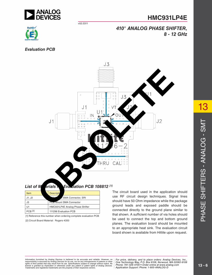
evaluation PCB
the circuit board used in the application should use rf circuit design techniques. signal lines should have 50 Ohm impedance while the package ground leads and exposed paddle should be connected directly to the ground plane similar to that shown. a sufficient number of via holes should be used to connect the top and bottom ground planes. the evaluation board should be mounted to an appropriate heat sink. the evaluation circuit board shown is available from hittite upon request.
list of Materials for evaluation PCB 108812 [1]
item Description
J1, J2 PCB Mount sMa Connector, sri
J3 PCB Mount sMa Connector
U1 hMC931LP4e analog Phase shifter
PCB [2] 111296 evaluation PCB
[1] reference this number when ordering complete evaluation PCB
[2] Circuit Board Material: rogers 4350
HMC931LP4Ev02.0311
410° AnAlog PhAse shifter,8 - 12 ghz
OBSOLETE
Information furnished by Analog Devices is believed to be accurate and reliable. However, no responsibility is assumed by Analog Devices for its use, nor for any infringements of patents or other rights of third parties that may result from its use. Specifications subject to change without notice. No license is granted by implication or otherwise under any patent or patent rights of Analog Devices. Trademarks and registered trademarks are the property of their respective owners.
For price, delivery, and to place orders: Analog Devices, Inc., One Technology Way, P.O. Box 9106, Norwood, MA 02062-9106 Phone: 781-329-4700 • Order online at www.analog.com Application Support: Phone: 1-800-ANALOG-D