Embed Size (px)
Citation preview
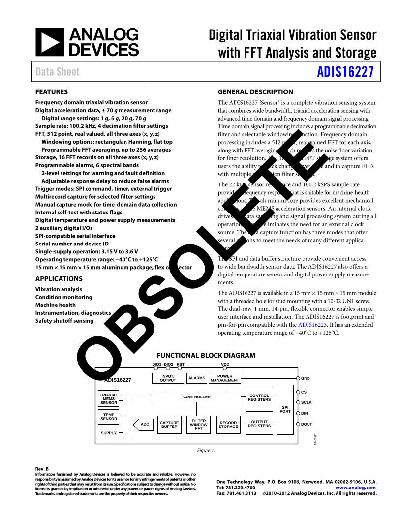
Digital Triaxial Vibration Sensor with FFT Analysis and Storage
Data Sheet ADIS16227
Rev. B Information furnished by Analog Devices is believed to be accurate and reliable. However, no responsibility is assumed by Analog Devices for its use, nor for any infringements of patents or other rights of third parties that may result from its use. Specifications subject to change without notice. No license is granted by implication or otherwise under any patent or patent rights of Analog Devices. Trademarks and registered trademarks are the property of their respective owners.
One Technology Way, P.O. Box 9106, Norwood, MA 02062-9106, U.S.A. Tel: 781.329.4700 www.analog.com Fax: 781.461.3113 ©2010–2012 Analog Devices, Inc. All rights reserved.
FEATURES Frequency domain triaxial vibration sensor Digital acceleration data, ± 70 g measurement range
Digital range settings: 1 g, 5 g, 20 g, 70 g Sample rate: 100.2 kHz, 4 decimation filter settings FFT, 512 point, real valued, all three axes (x, y, z)
Windowing options: rectangular, Hanning, flat top Programmable FFT averaging, up to 256 averages
Storage, 16 FFT records on all three axes (x, y, z) Programmable alarms, 6 spectral bands
2-level settings for warning and fault definition Adjustable response delay to reduce false alarms
Trigger modes: SPI command, timer, external trigger Multirecord capture for selected filter settings Manual capture mode for time-domain data collection Internal self-test with status flags Digital temperature and power supply measurements 2 auxiliary digital I/Os SPI-compatible serial interface Serial number and device ID Single-supply operation: 3.15 V to 3.6 V Operating temperature range: −40°C to +125°C 15 mm × 15 mm × 15 mm aluminum package, flex connector
APPLICATIONS Vibration analysis Condition monitoring Machine health Instrumentation, diagnostics Safety shutoff sensing
GENERAL DESCRIPTION The ADIS16227 iSensor® is a complete vibration sensing system that combines wide bandwidth, triaxial acceleration sensing with advanced time domain and frequency domain signal processing. Time domain signal processing includes a programmable decimation filter and selectable windowing function. Frequency domain processing includes a 512 point, real-valued FFT for each axis, along with FFT averaging, which reduces the noise floor variation for finer resolution. The 16-record FFT storage system offers users the ability to track changes over time and to capture FFTs with multiple decimation filter settings.
The 22 kHz sensor resonance and 100.2 kSPS sample rate provide a frequency response that is suitable for machine-health applications. The aluminum core provides excellent mechanical coupling to the MEMS acceleration sensors. An internal clock drives the data sampling and signal processing system during all operations, which eliminates the need for an external clock source. The data capture function has three modes that offer several options to meet the needs of many different applica-tions.
The SPI and data buffer structure provide convenient access to wide bandwidth sensor data. The ADIS16227 also offers a digital temperature sensor and digital power supply measure-ments.
The ADIS16227 is available in a 15 mm × 15 mm × 15 mm module with a threaded hole for stud mounting with a 10-32 UNF screw. The dual-row, 1 mm, 14-pin, flexible connector enables simple user interface and installation. The ADIS16227 is footprint and pin-for-pin compatible with the ADIS16223. It has an extended operating temperature range of −40°C to +125°C.
FUNCTIONAL BLOCK DIAGRAM
ADIS16227
RECORDSTORAGE
ALARMSINPUT/OUTPUT
CONTROLLER
ADC
TRIAXIALMEMS
SENSOR
TEMPSENSOR
SUPPLY
POWERMANAGEMENT
CS
SCLK
DIN
DOUT
GND
VDDRSTDIO1 DIO2
0942
5-00
1
CONTROLREGISTERS
SPIPORT
OUTPUTREGISTERS
FILTERWINDOW
FFTCAPTUREBUFFER
Figure 1.
OBSOLETE

ADIS16227 Data Sheet
Rev. B | Page 2 of 24
TABLE OF CONTENTS Features .............................................................................................. 1 Applications ....................................................................................... 1 General Description ......................................................................... 1 Functional Block Diagram .............................................................. 1 Revision History ............................................................................... 2 Specifications ..................................................................................... 3
Timing Specifications .................................................................. 4 Absolute Maximum Ratings ............................................................ 5
ESD Caution .................................................................................. 5 Pin Configuration and Function Descriptions ............................. 6 Theory of Operation ........................................................................ 7
Sensing Element ........................................................................... 7 Signal Processing .......................................................................... 7 User Interface ................................................................................ 7
Basic Operation ................................................................................. 8 SPI Write Commands .................................................................. 8 SPI Read Commands ................................................................... 8
Data Recording and Signal Processing ........................................ 10 Recording Modes ........................................................................ 10 Recording Times ......................................................................... 10 Power-Down ............................................................................... 11 Record Storage Mode ................................................................. 11 Sample Rate Options .................................................................. 11 Windowing Options ................................................................... 11 Range ............................................................................................ 12 Offset Correction ........................................................................ 12 FFT Averaging ............................................................................ 12 FFT Record Flash Endurance ................................................... 12
Spectral Alarms ............................................................................... 13 Alarm Definition ........................................................................ 13 Alarm Indicator Signals ............................................................. 14 Alarm Flags and Conditions ..................................................... 15 Alarm Status ................................................................................ 15 Worst-Condition Monitoring ................................................... 15
Reading Output Data ..................................................................... 16 Reading Data from the Data Buffer ......................................... 16 Accessing FFT Record Data ...................................................... 16 Data Format ................................................................................ 16 Power Supply/Temperature ....................................................... 17 FFT Event Header ...................................................................... 17
System Tools .................................................................................... 18 Global Commands ..................................................................... 18 Status/Error Flags ....................................................................... 18 Operation Managment .............................................................. 18 Input/Output Functions ............................................................ 19 Self-Test ....................................................................................... 19 Flash Memory Management ..................................................... 20 Device Identification .................................................................. 20
Applications Information .............................................................. 21 Mounting Guidelines ................................................................. 21 Getting Started ............................................................................ 21 Interface Board ........................................................................... 21
Outline Dimensions ....................................................................... 22 Ordering Guide .......................................................................... 22
REVISION HISTORY 5/12—Rev. A to Rev. B Changes to Table 10 ........................................................................ 10 2/12—Rev. 0 to Rev. A Changes to Dual Memory Structure Section ................................ 7 Change to Table 14 ......................................................................... 11
Changes to Alarm Trigger Settings Section, Enable Alarm Settings Section, Table 27, Table 28, Table 30, and Table 31 ............................................................................................ 14 Change to Alarm Indicator Section ............................................. 19 10/10—Revision 0: Initial Version
OBSOLETE
Data Sheet ADIS16227
Rev. B | Page 3 of 24
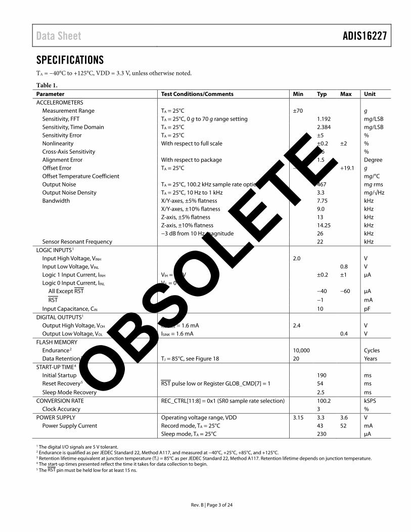
SPECIFICATIONS TA = −40°C to +125°C, VDD = 3.3 V, unless otherwise noted.
Table 1. Parameter Test Conditions/Comments Min Typ Max Unit ACCELEROMETERS
Measurement Range TA = 25°C ±70 g Sensitivity, FFT TA = 25°C, 0 g to 70 g range setting 1.192 mg/LSB Sensitivity, Time Domain TA = 25°C 2.384 mg/LSB Sensitivity Error TA = 25°C ±5 % Nonlinearity With respect to full scale ±0.2 ±2 % Cross-Axis Sensitivity 2.6 % Alignment Error With respect to package 1.5 Degree Offset Error TA = 25°C −19.1 +19.1 g Offset Temperature Coefficient 5 mg/°C Output Noise TA = 25°C, 100.2 kHz sample rate option 467 mg rms Output Noise Density TA = 25°C, 10 Hz to 1 kHz 3.3 mg/√Hz Bandwidth X/Y-axes, ±5% flatness 7.75 kHz X/Y-axes, ±10% flatness 9.0 kHz Z-axis, ±5% flatness 13 kHz Z-axis, ±10% flatness 14.25 kHz −3 dB from 10 Hz magnitude 26 kHz Sensor Resonant Frequency 22 kHz
LOGIC INPUTS1 Input High Voltage, VINH 2.0 V Input Low Voltage, VINL 0.8 V Logic 1 Input Current, IINH VIH = 3.3 V ±0.2 ±1 µA Logic 0 Input Current, IINL VIL = 0 V
All Except RST −40 −60 µA
RST −1 mA
Input Capacitance, CIN 10 pF DIGITAL OUTPUTS1
Output High Voltage, VOH ISOURCE = 1.6 mA 2.4 V Output Low Voltage, VOL ISINK = 1.6 mA 0.4 V
FLASH MEMORY Endurance2 10,000 Cycles Data Retention3 TJ = 85°C, see Figure 18 20 Years
START-UP TIME4 Initial Startup 190 ms Reset Recovery5 RST pulse low or Register GLOB_CMD[7] = 1 54 ms
Sleep Mode Recovery 2.5 ms CONVERSION RATE REC_CTRL[11:8] = 0x1 (SR0 sample rate selection) 100.2 kSPS
Clock Accuracy 3 % POWER SUPPLY Operating voltage range, VDD 3.15 3.3 3.6 V
Power Supply Current Record mode, TA = 25°C 43 52 mA Sleep mode, TA = 25°C 230 µA 1 The digital I/O signals are 5 V tolerant. 2 Endurance is qualified as per JEDEC Standard 22, Method A117, and measured at −40°C, +25°C, +85°C, and +125°C. 3 Retention lifetime equivalent at junction temperature (TJ) = 85°C as per JEDEC Standard 22, Method A117. Retention lifetime depends on junction temperature. 4 The start-up times presented reflect the time it takes for data collection to begin. 5 The RST pin must be held low for at least 15 ns.
OBSOLETE
ADIS16227 Data Sheet
Rev. B | Page 4 of 24
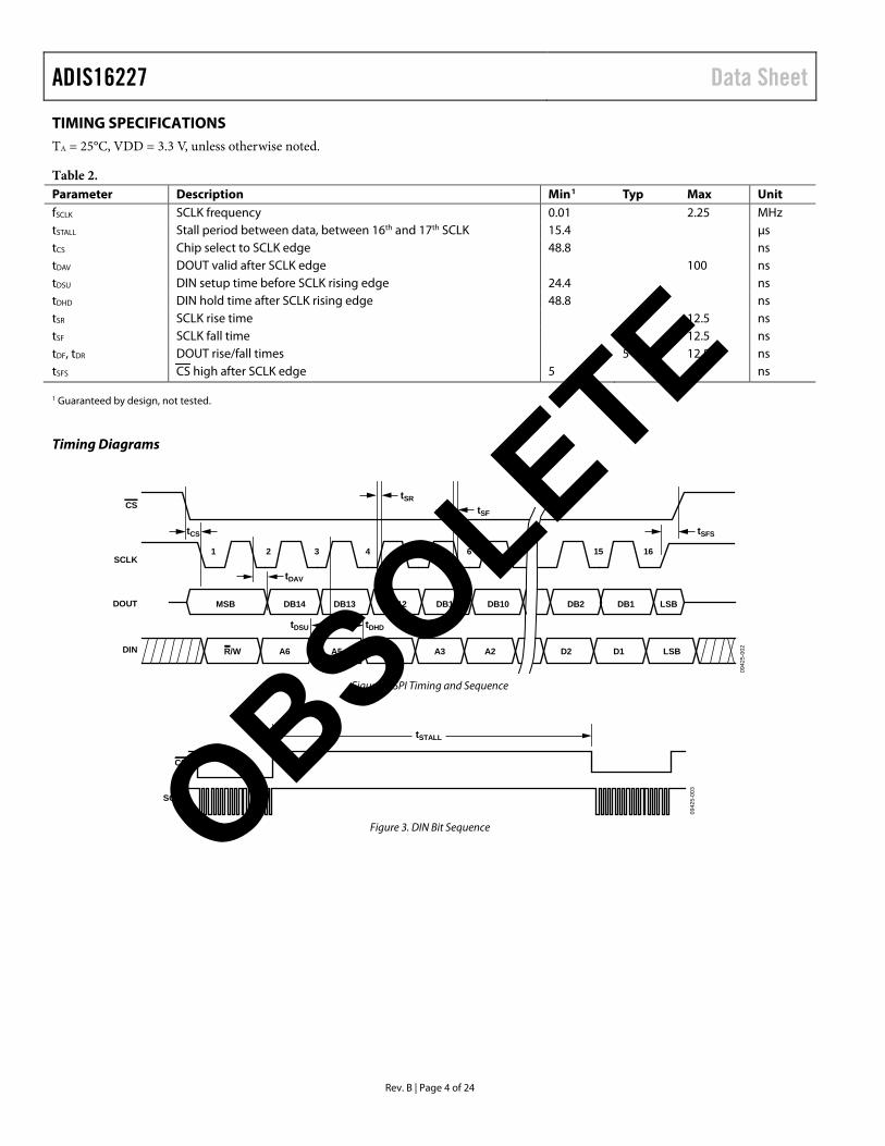
TIMING SPECIFICATIONS TA = 25°C, VDD = 3.3 V, unless otherwise noted.
Table 2. Parameter Description Min1 Typ Max Unit fSCLK SCLK frequency 0.01 2.25 MHz tSTALL Stall period between data, between 16th and 17th SCLK 15.4 µs tCS Chip select to SCLK edge 48.8 ns tDAV DOUT valid after SCLK edge 100 ns tDSU DIN setup time before SCLK rising edge 24.4 ns tDHD DIN hold time after SCLK rising edge 48.8 ns tSR SCLK rise time 12.5 ns tSF SCLK fall time 12.5 ns tDF, tDR DOUT rise/fall times 5 12.5 ns tSFS CS high after SCLK edge 5 ns 1 Guaranteed by design, not tested.
Timing Diagrams
CS
SCLK
DOUT
DIN
1 2 3 4 5 6 15 16
R/W A5A6 A4 A3 A2 D2
MSB DB14
D1 LSB
DB13 DB12 DB10DB11 DB2 LSBDB1
tCS tSFS
tDAV
tSRtSF
tDHDtDSU
0942
5-00
2
Figure 2. SPI Timing and Sequence
CS
SCLK
tSTALL
0942
5-00
3
Figure 3. DIN Bit Sequence
OBSOLETE

Data Sheet ADIS16227
Rev. B | Page 5 of 24
ABSOLUTE MAXIMUM RATINGS Table 3. Parameter Rating Acceleration
Any Axis, Unpowered 2000 g Any Axis, Powered 2000 g
VDD to GND −0.3 V to +6.0 V Digital Input Voltage to GND −0.3 V to +5.3 V Digital Output Voltage to GND −0.3 V to +3.6 V Analog Inputs to GND −0.3 V to +3.6 V Operating Temperature Range −40°C to +125°C Storage Temperature Range −65°C to +150°C
Stresses above those listed under Absolute Maximum Ratings may cause permanent damage to the device. This is a stress rating only; functional operation of the device at these or any other conditions above those indicated in the operational section of this specification is not implied. Exposure to absolute maximum rating conditions for extended periods may affect device reliability.
Table 4. Package Characteristics Package Type θJA θJC Device Weight 14-Lead Module 31°C/W 11°C/W 6.5 grams
ESD CAUTION
OBSOLETE

ADIS16227 Data Sheet
Rev. B | Page 6 of 24
PIN CONFIGURATION AND FUNCTION DESCRIPTIONS
14
13
12
11
10
9
8
7
6
5
4
3
2
1
PIN 13 PIN 1
PIN 2
aX
aZ
aY
TOP VIEWLOOK THROUGH
PINS ARE NOT VISIBLEFROM THIS VIEW
1. THE ARROWS ASSOCIATED WITH aX, aY, AND aZ DEFINE THE DIRECTION OF VELOCITY CHANGE THAT PRODUCES A POSITIVE OUTPUT IN ACCELERATION OUTPUT REGISTERS.2. MATING CONNECTOR EXAMPLE: SAMTEC P/N CLM-107-02-LM-D-A. 09
425-
004
Figure 4. Pin Configuration
Table 5. Pin Function Descriptions Pin No. Mnemonic Type1 Description 1, 4, 9, 10 GND S Ground 2, 6 NC I No Connect 3 DIO2 I/O Digital Input/Output Line 2 5 DIO1 I/O Digital Input/Output Line 1 7 RST I Reset, Active Low
8 VDD S Power Supply, 3.3 V 11 DIN I SPI, Data Input 12 DOUT O2 SPI, Data Output 13 SCLK I SPI, Serial Clock 14 CS I SPI, Chip Select 1 S is supply, O is output, I is input, and I/O is input/output. 2 DOUT is an output when CS is low. When CS is high, DOUT is in a three-state, high impedance mode.
OBSOLETE

Data Sheet ADIS16227
Rev. B | Page 7 of 24
THEORY OF OPERATION The ADIS16227 is a triaxial, wide bandwidth, vibration-sensing system. It combines a triaxial MEMS accelerometer with a sampling and advanced signal processing system. The SPI-compatible port and user register structure provide convenient access to frequency domain vibration data and many user controls.
SENSING ELEMENT Digital vibration sensing in the ADIS16227 starts with a wide bandwidth MEMS accelerometer core on each axis, which provides a linear motion-to-electrical transducer function. Figure 5 provides a basic physical diagram of the sensing element and its response to linear acceleration. It uses a fixed frame and a moving frame to form a differential capacitance network that responds to linear acceleration. Tiny springs tether the moving frame to the fixed frame and govern the relationship between acceleration and physical displacement. A modulation signal on the moving plate feeds through each capacitive path into the fixed frame plates and into a demodulation circuit, which produces the electrical signal that is proportional to the acceleration acting on the device.
MOVABLEFRAME
A
CC
ELER
ATI
ON
UNITFORCINGCELL
UNIT SENSINGCELL
MOVINGPLATE
FIXEDPLATES
PLATECAPACITORS
ANCHOR
ANCHOR
0942
5-00
5
Figure 5. MEMS Sensor Diagram
SIGNAL PROCESSING Figure 6 offers a simplified block diagram for the ADIS16227. The signal processing stage includes time domain data capture, digital decimation/filtering, windowing, FFT analysis, FFT averaging, and record storage. See Figure 13 for more details on the signal processing operation.
TRIAXIALMEMS
SENSOR
CLOCK
CONTROLLER
CAPTUREBUFFER
CONTROLREGISTERS
SPI S
IGN
ALS
SPI P
OR
T
OUTPUTREGISTERS
TEMPSENSOR
ADC
0942
5-00
6
Figure 6. Simplified Sensor Signal Processing Diagram
USER INTERFACE SPI Interface
The user registers manage user access to both sensor data and configuration inputs. Each 16-bit register has its own unique bit assignment and two addresses: one for its upper byte and one for its lower byte. Table 8 provides a memory map for each register, along with its function and lower byte address. The data collection and configuration command uses the SPI, which consists of four wires. The chip select (CS) signal activates the SPI interface, and the serial clock (SCLK) synchronizes the serial data lines. Input commands clock into the DIN pin, one bit at a time, on the SCLK rising edge. Output data clocks out of the DOUT pin on the SCLK falling edge. When the SPI is used as a slave device, the DOUT contents reflect the information requested using a DIN command.
Dual Memory Structure
The user registers provide addressing for all input/output operations in the SPI interface. The control registers use a dual memory structure. The controller uses SRAM registers for normal operation, including user-configuration commands. The flash memory provides nonvolatile storage for control registers that have flash backup (see Table 8). Storing configuration data in the flash memory requires a manual flash update command (GLOB_CMD[6] = 1, DIN = 0xBE40). When the device powers on or resets, the flash memory contents load into the SRAM, and the device starts producing data according to the configuration in the control registers.
NONVOLATILEFLASH MEMORY(NO SPI ACCESS)
MANUALFLASH
BACKUP
START-UPRESET
VOLATILESRAM
SPI ACCESS
0942
5-00
7
Figure 7. SRAM and Flash Memory Diagram
OBSOLETE

ADIS16227 Data Sheet
Rev. B | Page 8 of 24
BASIC OPERATION The ADIS16227 uses a SPI for communication, which enables a simple connection with a compatible, embedded processor platform, as shown in Figure 8. The factory default configuration for DIO1 provides a busy indicator signal that transitions low when an event completes and data is available for user access. Use the DIO_CTRL register (see Table 59) to reconfigure DIO1 and DIO2, if necessary.
SYSTEMPROCESSORSPI MASTER
ADIS16227SPI SLAVE
SCLK
CS
DIN
DOUT
SCLK
SS
MOSI
MISO
IRQ1 DIO1
VDD
IRQ2 DIO2
+3.3V
8
14
1 4 9 10
13
11
12
5
3
0942
5-00
8
Figure 8. Electrical Hook-Up Diagram
Table 6. Generic Master Processor Pin Names and Functions Pin Name Function SS Slave select
IRQ1, IRQ2 Interrupt request inputs (optional) MOSI Master output, slave input MISO Master input, slave output SCLK Serial clock
The ADIS16227 SPI interface supports full duplex serial communication (simultaneous transmit and receive) and uses the bit sequence shown in Figure 12. Table 7 provides a list of the most common settings that require attention to initialize a processor serial port for the ADIS16227 SPI interface.
Table 7. Generic Master Processor SPI Settings Processor Setting Description Master ADIS16227 operates as a slave. SCLK Rate ≤ 2.25 MHz Bit rate setting. SPI Mode 3 Clock polarity/phase
(CPOL = 1, CPHA = 1). MSB-First Bit sequence. 16-Bit Shift register/data length.
Table 8 provides a list of user registers with their lower byte addresses. Each register consists of two bytes that each have their own, unique 7-bit addresses. Figure 9 relates each register’s bits to their upper and lower addresses.
UPPER BYTE
15 14 13 12 11 10 9 8 7 6 5 4 3 2 1 0
LOWER BYTE
0942
5-00
9
Figure 9. Generic Register Bit Definitions
SPI WRITE COMMANDS User control registers govern many internal operations. The DIN bit sequence in Figure 12 provides the ability to write to these registers, one byte at a time. Some configuration changes and functions require only one write cycle. For example, set GLOB_CMD[11] = 1 (DIN = 0xBF08) to start a manual capture sequence. The manual capture starts immediately after the last bit clocks into DIN (16th SCLK rising edge). Other configurations may require writing to both bytes.
CS
DIN
SCLK
0942
5-01
0
Figure 10. SPI Sequence for Manual Capture Start (DIN = 0xBF08)
SPI READ COMMANDS A single register read requires two 16-bit SPI cycles that also use the bit assignments in Figure 12. The first sequence sets R/W = 0 and communicates the target address (Bits[A6:A0]). Bits[D7:D0] are don’t care bits for a read DIN sequence. DOUT clocks out the requested register contents during the second sequence. The second sequence can also use DIN to set up the next read. Figure 11 provides a signal diagram for all four SPI signals while reading the PROD_ID register (see Table 63) pattern. In this diagram, DIN = 0x5600 and DOUT reflect the decimal equivalent of 16,227.
DOUT = 0011 1111 0110 0011 = 0x3F63 = 16,227 = PROD_ID
SCLK
CS
DIN
DOUT
0942
5-01
1
Figure 11. Example SPI Read, PROD_ID, Second Sequence
R/W R/WA6 A5 A4 A3 A2 A1 A0 D7 D6 D5 D4 D3 D2 D1 D0
DB0DB1DB2DB3DB4DB5DB6DB7DB8DB9DB10DB11DB12DB13DB14DB15
NOTES1. DOUT BITS ARE BASED ON THE PREVIOUS 16-BIT SEQUENCE (R/W = 0).
CS
SCLK
DIN
DOUT
A6 A5
DB13DB14DB15
0942
5-01
2
Figure 12. Example SPI Read Sequence
OBSOLETE

Data Sheet ADIS16227
Rev. B | Page 9 of 24
Table 8. User Register Memory Map Register Name Access
Flash Backup Address Default Function Reference
FLASH_CNT Read only Yes 0x00 N/A Status, flash memory write count Table 61 X_NULL Read only Yes 0x02 0x0000 X-axis accelerometer offset correction Table 18 Y_NULL Read only Yes 0x04 0x0000 Y-axis accelerometer offset correction Table 18 Z_NULL Read only Yes 0x06 0x0000 Z-axis accelerometer offset correction Table 18 REC_FLSH_CNT N/A No 0x08 N/A Record flash write/erase counter Table 20 SUPPLY_OUT Read only Yes 0x0A 0x8000 Output, power supply during capture Table 48 TEMP_OUT Read only Yes 0x0C 0x8000 Output, temperature during capture Table 50 FFT_AVG Read/write Yes 0x0E 0x0008 Control, number of FFT records to average Table 19 BUF_PNTR Read/write Yes 0x10 0x0000 Control, buffer address pointer Table 43 REC_PNTR Read/write Yes 0x12 0x0000 Control, record address pointer Table 44 X_BUF Read only No 0x14 0x8000 Output, buffer for x-axis acceleration data Table 45 Y_BUF Read only No 0x16 0x8000 Output, buffer for y-axis acceleration data Table 45 Z_BUF Read only No 0x18 0x8000 Output, buffer for z-axis acceleration data Table 45 REC_CNTR Read/write No 0x1A 0x0000 Control, record counter Table 13 REC_CTRL Read/write Yes 0x1C 0x1130 Control, record control register Table 10 REC_PRD Read/write Yes 0x1E 0x0000 Control, record period (automatic mode) Table 11 ALM_F_LOW Read/write N/A 0x20 0x0000 Alarm, spectral band lower frequency limit Table 24 ALM_F_HIGH Read/write N/A 0x22 0x0000 Alarm, spectral band upper frequency limit Table 25 ALM_X_MAG1 Read/write N/A 0x24 0x0000 Alarm, x-axis, Alarm 1 level Table 26 ALM_Y_MAG1 Read/write N/A 0x26 0x0000 Alarm, y-axis, Alarm 1 level Table 27 ALM_Z_MAG1 Read/write N/A 0x28 0x0000 Alarm, z-axis, Alarm 1 level Table 28 ALM_X_MAG2 Read/write N/A 0x2A 0x0000 Alarm, x-axis, Alarm 2 level Table 29 ALM_Y_MAG2 Read/write N/A 0x2C 0x0000 Alarm, y-axis, Alarm 2 level Table 30 ALM_Z_MAG2 Read/write N/A 0x2E 0x0000 Alarm, z-axis, Alarm 2 level Table 31 ALM_PNTR Read/write Yes 0x30 0x0000 Alarm, spectral alarm band pointer Table 23 ALM_S_MAG Read/write Yes 0x32 0x0000 Alarm, system alarm level Table 32 ALM_CTRL Read/write Yes 0x34 0x0080 Alarm, configuration Table 22 DIO_CTRL Read/write Yes 0x36 0x000F Control, functional I/O configuration Table 59 GPIO_CTRL Read/write Yes 0x38 0x0000 Control, general-purpose I/O Table 60 Reserved N/A N/A 0x3A N/A Reserved N/A DIAG_STAT Read only No 0x3C 0x0000 Status, system error flags Table 58 GLOB_CMD Write only No 0x3E N/A Control, global command register Table 57 ALM_X_STAT Read only N/A 0x40 0x0000 Alarm, x-axis, status for spectral alarm bands Table 33 ALM_Y_STAT Read only N/A 0x42 0x0000 Alarm, y-axis, status for spectral alarm bands Table 34 ALM_Z_STAT Read only N/A 0x44 0x0000 Alarm, z-axis, status for spectral alarm bands Table 35 ALM_X_PEAK Read only N/A 0x46 0x0000 Alarm, x-axis, peak value (most severe alarm) Table 36 ALM_Y_PEAK Read only N/A 0x48 0x0000 Alarm, y-axis, peak value (most severe alarm) Table 37 ALM_Z_PEAK Read only N/A 0x4A 0x0000 Alarm, z-axis, peak value (most severe alarm) Table 38 TIME_STAMP_L Read only N/A 0x4C 0x0000 Record time stamp, lower word Table 54 TIME_STAMP_H Read only N/A 0x4E 0x0000 Record time stamp, upper word Table 55 Reserved N/A N/A 0x50 to 0x51 N/A Reserved N/A LOT_ID1 Read only Yes 0x52 N/A Lot identification code Table 62 LOT_ID2 Read only Yes 0x54 N/A Lot identification code Table 62 PROD_ID Read only Yes 0x56 0x3F63 Product identifier; convert to decimal = 16,227 Table 63 SERIAL_NUM Read only Yes 0x58 N/A Serial number Table 64 ALM_X_FREQ Read only N/A 0x70 0x0000 Alarm, x-axis, frequency of most severe alarm Table 39 ALM_Y_FREQ Read only N/A 0x72 0x0000 Alarm, y-axis, frequency of most severe alarm Table 40 ALM_Z_FREQ Read only N/A 0x74 0x0000 Alarm, z-axis, frequency of most severe alarm Table 41 REC_INFO Read only N/A 0x76 N/A Record settings Table 53
OBSOLETE

ADIS16227 Data Sheet
Rev. B | Page 10 of 24
DATA RECORDING AND SIGNAL PROCESSING The ADIS16227 provides a number of registers for configuring its data collection and signal processing operation (see Table 9). Figure 13 provides a signal flow diagram, which describes many of these settings.
Table 9. Sampling/Signal Processing Register Summary Register Address Description X_NULL 0x02 X-axis offset correction Y_NULL 0x04 Y-axis offset correction Z_NULL 0x06 Z-axis offset correction REC_FLSH_CNT 0x08 Record, flash write cycle counter FFT_AVG 0x0E Record, FFT averages REC_CNTR 0x1A Record, counter REC_CTRL 0x1C Record, data processing REC_PRD 0x1E Record, automatic mode period GLOB_CMD 0x3E Trigger, record commands
The record control register is REC_CTRL (see Table 10), which provides external controls for sample rates, dynamic range, record storage, recording mode, and power management.
Table 10. REC_CTRL Bit Descriptions Bits Description (Default = 0x1130) [15:14] Not used [13:12] Window setting:
00 = rectangular, 01 = Hanning, 10 = flat top, 11 = N/A [11] SR3, fs ÷ 512 (1 = enabled for analysis) [10] SR2, fs ÷ 64 (1 = enabled for analysis) [9] SR1, fs ÷ 8 (1 = enabled for analysis) [8] SR0, fs (1 = enabled for analysis) [7] Power-down between each recording (1 = enabled) [6] Not used [5:4] Signal range:
00 = 0 g to 1 g, 01 = 0 g to 5 g, 10 = 0 g to 20 g, 11 = 0 g to 70 g
[3:2] Storage method: 00 = none, 01 = alarm trigger, 10 = all, 11 = N/A
[1:0] Recording mode: 00 = manual, 01 = automatic, 10 = manual time, 11 = N/A
RECORDING MODES REC_CTRL[1:0] provides three modes for triggering: (1) manual, (2) automatic, and (3) manual time domain. The manual and automatic modes produce FFT events, which include data collection, filtering, windowing, FFT analysis, and record storage (if selected). The manual time domain mode produces time-domain data in the buffer. All three modes require an external trigger, using either the SPI interface or one of the auxiliary digital I/O lines, DIO1 or DIO2. For the SPI external trigger option, set GLOB_CMD[11] = 1 (DIN = 0x3F08). For the digital I/O option, use the DIO_CTRL register (see Table 59) to configure either DIO1 or DIO2 as an external trigger input.
For example, set DIO_CTRL[7:0] = 0x2F (DIN = 0xB62F) to configure DIO2 as a positive external trigger input and maintain the DIO1 factory default configuration as a positive busy indicator. In manual mode, the start command triggers a recording for an averaged FFT and stops after the recording is complete. In automatic mode, the start command executes a recording, and a timer continues to trigger recordings based on the record period setting in REC_PRD (see Table 11).
Table 11. REC_PRD Register Bit Descriptions Bits Description (Default = 0x0000) [15:10] Not used [9:8] Scale for data bits 00 = 1 second/LSB 01 = 1 minute/LSB 10 = 1 hour/LSB [7:0] Data bits, binary format, range = 0 to 255
RECORDING TIMES The automatic recording period (REC_PRD) must be greater than the total recording time. Use the following equations to calculate the recording time:
Manual time mode
ASTSTPTSR TTTTT +++=
FFT modes
( ) ASTSTFFTPTSFR TTTTTNT ++++×=
The storage time (TST) applies only when a storage method is selected in REC_CTRL[3:2]. See Table 10 for more details on the record storage setting. The alarm scan time (TAST) applies only when the alarms are enabled in ALM_CTRL[4:0]. See Table 22 for more details on enabling the alarms.
Table 12. Available Records Function Time (ms) Sample Time, TS See Table 15 Processing Time, TPT 10.4 FFT Time, TFFT 26.6 Number of FFT Averages, NF See Table 19 Storage Time, TST 120.0 Alarm Scan Time, TAST 2.21 OBSOLETE

Data Sheet ADIS16227
Rev. B | Page 11 of 24
POWER-DOWN Set GLOB_CMD[1] = 1 (DIN = 0xBE02) to power down the ADIS16227. To reduce power consumption, set REC_CTRL[7] = 1 to automatically power down after a record has completed. Toggle the CS line from high to low to wake the device up and place it in an idle state, where it waits for the next command. When configured as an external trigger option, toggling DIO1 or DIO2 can wake the device up as well. Using DIO1 or DIO2 for this purpose avoids the potential for multiple devices contending for DOUT when waking up with the CS line approach. After completing the record cycle, the device remains awake. Use GLOB_CMD[1] to put it back to sleep after reading the record data.
RECORD STORAGE MODE After the ADIS16227 finishes processing FFT data, it stores the data into the FFT buffer, where it is available for external access using the SPI and x_BUF registers. REC_CTRL[3:2] provides programmable conditions for writing buffer data into the FFT records, which are in nonvolatile flash memory locations. Set REC_CTRL[3:2] = 01 to store FFT buffer data into the flash memory records only when an alarm condition is met. Set REC_CTRL[3:2] = 10 to store every set of FFT data into the flash memory locations. The flash memory record provides space for a total of 16 records. Each record stored in flash memory contains a header and frequency domain (FFT) data from all three axes (x, y, and z). When all 16 records are full, new records do not load into the flash memory. The REC_CNTR register (see Table 13) provides a running count for the number of records that are stored. Set GLOB_CMD[8] = 1 (DIN = 0xBF01) to clear all of the records in flash memory.
Table 13. REC_CNTR Bit Descriptions Bits Description (Default = 0x0000) [15:5] Not used [4:0] Total number of records taken, range = 0 to 16, binary
SAMPLE RATE OPTIONS The analog-to-digital converter (ADC) samples each accelero-meter sensor at a rate of 100.2 kSPS (fs). REC_CTRL[11:8] provide four different sample rate options for FFT analysis: SR0 (fs), SR1(fs ÷ 8), SR2 (fs ÷ 64), and SR3 (fs ÷ 512). The reduced rates come from a decimation filter, which reduces the bandwidth and bin widths. See Figure 13 for the filter location in the signal processing diagram and Table 14 for the performance trade-offs associated with each sample rate setting.
Table 14. Sample Rate Settings and Filter Performance
Setting Sample Rate (SPS)
Bin Width (Hz)
Bandwidth (Hz)
Noise (mg)
SR0 100,189 196 26,000 467 SR1 12,524 25 6,262 260 SR2 1566 3.1 783 100 SR3 196 0.38 98 38
Table 15 provides the data sampling time (TS) for each sample rate setting. This represents the time it takes to record data for all three axes of vibration data.
Table 15. Sample Times, TS Sample Rate Setting Sample Time (ms), TS SR0, REC_CTRL[8] = 1 5.27 SR1, REC_CTRL[9] = 1 42.15 SR2, REC_CTRL[10] = 1 337.17 SR3, REC_CTRL[11] = 1 2697.39
If more than one sample rate setting is active in REC_CTRL[11:8], the sample rate setting automatically updates after each FFT event and waits for the next trigger input. The order of priority starts with the highest sample rate enabled and works toward the lowest after each REC_CTRL[11:8] write cycle. When used in conjunction with automatic trigger mode and record storage, FFT analysis for each sample rate option requires no further user inputs, except for collecting the data. Depending on the number of FFT averages, the time period between each sample rate selection may be quite large. Note that selecting multiple sample rates reduces the number of records available for each sample rate setting, as shown in Table 16.
Table 16. Available Records Number of Sample Rates Selected Available Records 1 16 2 8 3 5 4 4
WINDOWING OPTIONS REC_CTRL[13:12] provide three options for pre-FFT windowing of time data. For example, set REC_CTRL[13:12] = 01 to use the Hanning window, which offers the best amplitude resolution of the peaks between frequency bins and minimal broadening of peak amplitudes. The rectangular and flat top windows are also available because they are common windowing options for vibration monitoring. The flat top window provides accurate amplitude resolution with a trade-off of broadening the peak amplitudes.
OBSOLETE

ADIS16227 Data Sheet
Rev. B | Page 12 of 24
RANGE REC_CTRL[5:4] provide four range options for scaling acceleration data prior to the FFT analysis stage. For example, set REC_CTRL[5:4] = 10 to set the peak acceleration (AMAX) to 5 g. See Table 17 for the resolution associated with each setting and Figure 13 for the location of this operation in the signal flow diagram.
Table 17. Range Setting and LSB Weights Range Setting (g) (REC_CTRL[5:4])
Time Mode (mg/LSB)
FFT Mode (mg/LSB)
0 to 1 0.0305 0.0153 0 to 5 0.1526 0.0763 0 to 20 0.6104 0.3052 0 to 70 2.3842 1.1921
OFFSET CORRECTION The x_NULL registers (see Table 18) contain the offset correction factors generated when using the internal, autonull command. They represent the KO factor in Figure 13 and follow the digital format in Table 18. Set GLOB_CMD[0] =1 (DIN = 0xBE01) and wait for 681 ms to execute this function.
Table 18. X_NULL, Y_NULL, and Z_NULL Bit Descriptions Bits Description (Default = 0x0000) [15:0] Offset correction factor, twos complement,
2.3842 mg/LSB
FFT AVERAGING The FFT averaging function records a programmable number of FFTs and combines them into a single, averaged FFT record. This function is useful in reducing the variation of the FFT noise floor, which enables detection of lower vibration levels. To enable this function, write the number of averages to FFT_AVG. Setting FFT_AVG = 0x0000 has the same effect as setting FFT_AVG = 0x0001: no averaging. Setting FFT_AVG ≥ 0x0100 results in a setting of 256. Therefore, set FFT_AVG[15:8] = 0x01 (DIN = 0x8F01) to establish the maximum average setting of 256. Another example configuration is to set FFT_AVG = 0x00F0 (DIN = 0x8F00, DIN = 0x8EF0) to establish an average setting of 240.
Table 19. FFT_AVG Register Bit Descriptions Bits Description (Default = 0x0008) [15:9] Not used [8:0] Number of FFT averages for a single record,
NF in Figure 13, range = 1 to 256, binary
FFT RECORD FLASH ENDURANCE The REC_FLSH_CNT register (see Table 20) increments each time that all 16 records have FFT data.
Table 20. REC_FLSH_CNT Bit Descriptions Bits Description [15:0] Flash write cycle count, record data only, binary
K = 1xKNA
Na1
÷NA
0942
5-01
6
TRIAXISMEMSACCEL 100kSPS +
Ko Ks
FFTFFT
AVERAGE(NF)
FFTBUFFER
BUFFERREGISTER AND SPI
FFTRECORD
1
FFTRECORD
m
FFTRECORD
15
SAMPLE RATE SETTINGREC_CTRL[11:8]
WINDOW SETTINGREC_CTRL[13:12]
OFFSET CORRECTIONKO = X_NULL, Y_NULL, Z_NULL
RANGE-SCALE SETTINGKs= AMAX ÷ 215AMAX = PEAK FROM REC_CTRL[5:4] FFT
RECORD0
NF = # OF AVERAGESNF = FFT_AVG[8:0]
FFT RECORDS—NONVOLATILE FLASH MEMORY
m = REC_CNTRREC_CTRL[3:2]
WINDOW
Figure 13. Signal Flow Diagram, REC_CTRL[1:0] = 00 or 01, FFT Analysis Modes
OBSOLETE

Data Sheet ADIS16227
Rev. B | Page 13 of 24
SPECTRAL ALARMS The alarm function offers six spectral bands for alarm detection. Each spectral band has high and low frequency definitions, along with two different trigger thresholds (Alarm 1 and Alarm 2) for each accelerometer axis. Table 21 provides a summary of each register used to configure the alarm function.
Table 21. Alarm Function Register Summary Register Address Description ALM_F_LOW 0x20 Alarm frequency, lower limit ALM_F_HIGH 0x22 Alarm frequency, upper limit ALM_X_MAG1 0x24 X-Alarm Trigger Level 1 (warning) ALM_Y_MAG1 0x26 Y-Alarm Trigger Level 1 (warning) ALM_Z_MAG1 0x28 Z-Alarm Trigger Level 1 (warning) ALM_X_MAG2 0x2A X-Alarm Trigger Level 2 (fault) ALM_Y_MAG2 0x2C Y-Alarm Trigger Level 2 (fault) ALM_Z_MAG2 0x2E Z-Alarm Trigger Level 2 (fault) ALM_PNTR 0x30 Alarm pointer ALM_S_MAG 0x32 System alarm trigger level ALM_CTRL 0x34 Alarm configuration DIAG_STAT 0x3C Alarm status ALM_X_STAT 0x40 X-alarm status ALM_Y_STAT 0x42 Y-alarm status ALM_Z_STAT 0x44 Z-alarm status ALM_X_PEAK 0x46 X-alarm peak ALM_Y_PEAK 0x48 Y-alarm peak ALM_Z_PEAK 0x4A Z-alarm peak ALM_X_FREQ 0x70 X-axis alarm frequency of peak alarm ALM_Y_FREQ 0x72 Y-axis alarm frequency of peak alarm ALM_Z_FREQ 0x74 Z-axis alarm frequency of peak alarm
The ALM_CTRL register (see Table 22) provides control bits that enable each axis’ spectral alarms, configures the system alarm, sets the record delay for the spectral alarms, and configures the clearing function for the DIAG_STAT error flags.
Table 22. ALM_CTRL Bit Descriptions Bits Description (Default = 0x0080) [15:12] Not used [11:8] Response delay, range: 0 to 15; represents the number
of spectral records for each spectral alarm before a spectral alarm flag is set high
[7] Latch DIAG_STAT error flags, which requires a clear status command (GLOB_CMD[4]) to reset the flags to 0 (1 = enabled, 0 = disabled)
[6] Enable DIO1 as an Alarm 1 output indicator and enable DIO2 as an Alarm2 output indicator (1 = enabled)
[5] System alarm comparison polarity 1 = trigger when less than ALM_MAGS[11:0] 0 = trigger when greater than ALM_MAGS[11:0] [4] System alarm, 1 = temperature 0 = power supply [3] Alarm S enable (ALM_S_MAG), 1 = enabled, 0 = disabled [2] Alarm Z enable (ALM_Z_MAG), 1 = enabled, 0 = disabled [1] Alarm Y enable (ALM_Y_MAG), 1 = enabled, 0 = disabled [0] Alarm X enable (ALM_X_MAG), 1 = enabled, 0 = disabled
ALARM DEFINITION The alarm function provides six programmable spectral bands, as shown in Figure 14. Each spectral alarm band has lower and upper frequency definitions for all four sample rate options. It also has two independent trigger level settings, which are useful for systems that value warning and fault condition indicators.
MA
GN
ITU
DE
FREQUENCY 0942
5-02
0
1 2 3 4 5 6
ALM_F_HIGHALM_F_LOW
ALM_x_MAG1ALM_x_MAG2
Figure 14. Spectral Band Alarm Setting Example, ALM_PNTR = 0x03
Select the spectral band for configuration by writing its number (1 to 6) to ALM_PNTR[2:0] (see Table 23). Then, select the sample rate setting using ALM_PNTR[9:8]. This number represents a binary number, which corresponds to the x in the SRx sample rates settings associated with REC_CTRL[11:8] (see Table 10). For example set ALM_PNTR[7:0] = 0x05 (DIN = 0xB005) to select Alarm Spectral Band 5 and set ALM_PNTR[15:8] = 0x02 (DIN = 0xB102) to select the SR2 sample rate option from Table 14, 1,566 SPS.
Table 23. ALM_PNTR Bit Assignments Bits Description (Default = 0x0000) [15:10] Not used [9:8] Sample rate setting, range: 0 to 3 [7:3] Not used [2:0] Spectral band number, range: 1 to 6 OBSOLETE

ADIS16227 Data Sheet
Rev. B | Page 14 of 24
Alarm Band Frequency Definitions
After the spectral band and sample rate settings are set, program the lower and upper frequency boundaries by writing their bin numbers to the ALM_F_LOW (see Table 24) and ALM_F_HIGH (see Table 25) registers. Use the bin width definitions in Table 14 to convert a frequency into a bin number for this definition. Calculate the bin number by dividing the frequency by the bin width associated with the sample rate setting. For example, 3400 Hz, divided by 196 Hz/bin (SR0 setting), rounded to the nearest integer, is equal to 17, or 0x12. Therefore, set ALM_F_LOW[7:0] = 0x11 (DIN = 0xA011) to establish 3400 Hz as the lower frequency for the SR0 sample rate setting.
Table 24. ALM_F_LOW Bit Assignments Bits Description (Default = 0x0000) [15:8] Not used [7:0] Lower frequency, bin number, range = 0 to 255
Table 25. ALM_F_HIGH Bit Assignments Bits Description (Default = 0x0000) [15:8] Not used [7:0] Upper frequency, bin number, range = 0 to 255
Alarm Trigger Settings
The ALM_x_MAG1 and ALM_x_MAG2 registers provide two independent trigger settings for all three axes of acceleration data. They use the data format established by the range setting in REC_CTRL[5:4] and recording mode in REC_CTRL[1:0]. For example, when using the 0 g to 1 g mode for FFT analysis, 3277 LSB is equivalent to 500.07 mg. To set the critical alarm to 500.07 mg when using the 0 g to 1 g range option in REC_CTRL2 for FFT records, set ALM_X_MAG2 = 0x0CCD (DIN = 0xAD0C, 0xACCD). See Table 10 and Table 17 for more information on formatting each trigger level. Note that trigger settings associated with Alarm 2 should be greater than the trigger settings for Alarm 1. In other words, the alarm magnitude settings should meet the following criteria:
ALM_X_MAG2 > ALM_X_MAG1 ALM_Y_MAG2 > ALM_Y_MAG1 ALM_Z_MAG2 > ALM_Z_MAG1
Table 26. ALM_X_MAG1 Bit Assignments Bits Description (Default = 0x0000) [15:0] X-axis Alarm Trigger Level 1, 16-bit unsigned; see
REC_CTRL[5:4] and Table 17 for the scale factor
Table 27. ALM_Y_MAG1 Bit Assignments Bits Description (Default = 0x0000) [15:0] Y-axis Alarm Trigger Level 1, 16-bit unsigned; see
REC_CTRL[5:4] and Table 17 for the scale factor
Table 28. ALM_Z_MAG1 Bit Assignments Bits Description (Default = 0x0000) [15:0] Z-axis Alarm Trigger Level 1, 16-bit unsigned; see
REC_CTRL[5:4] and Table 17 for the scale factor
Table 29. ALM_X_MAG2 Bit Assignments Bits Description (Default = 0x0000) [15:0] X-axis Alarm Trigger Level 2, 16-bit unsigned; see
REC_CTRL[5:4] and Table 17 for the scale factor
Table 30. ALM_Y_MAG2 Bit Assignments Bits Description (Default = 0x0000) [15:0] Y-axis Alarm Trigger Level 2, 16-bit unsigned; see
REC_CTRL[5:4] and Table 17 for the scale factor
Table 31. ALM_Z_MAG2 Bit Assignments Bits Description (Default = 0x0000) [15:0] Z-axis Alarm Trigger Level 1, 16-bit unsigned; see
REC_CTRL[5:4] and Table 17 for the scale factor
Table 32. ALM_S_MAG Bit Assignments Bits Description (Default = 0x0000) [15:0] System alarm trigger level, data format matches target
from ALM_CTRL[4]
Enable Alarm Settings
Before configuring the spectral alarm registers, clear their current contents by setting GLOB_CMD[9] = 1 (DIN = 0xBF02). After completing the spectral alarm band definitions, enable the settings by setting GLOB_CMD[12] = 1 (DIN = 0xBF10). The device ignores the save command if any of these locations have already been written to.
ALARM INDICATOR SIGNALS DIO_CTRL[5:2] and ALM_CTRL[6] provide controls for establishing DIO1 and DIO2 as dedicated alarm output indicator signals. Use DIO_CTRL[5:2] to select Alarm function for DIO1 and/or DIO2; then set ALM_CTRL[6] = 1 to enable DIO1 to serve as an Alarm 1 indicator and DIO2 as an Alarm 2 indicator. This setting establishes DIO1 to indicate Alarm 1 (warning) conditions and DIO2 to indicate Alarm 2 (critical) conditions. OBSOLETE
Data Sheet ADIS16227
Rev. B | Page 15 of 24
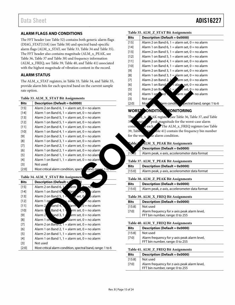
ALARM FLAGS AND CONDITIONS The FFT header (see Table 52) contains both generic alarm flags (DIAG_STAT[13:8] (see Table 58) and spectral band-specific alarm flags (ALM_x_STAT, see Table 33, Table 34 and Table 35). The FFT header also contains magnitude (ALM_x_PEAK, see Table 36, Table 37 and Table 38) and frequency information (ALM_x_FREQ, see Table 39, Table 40, and Table 41) associated with the highest magnitude of vibration content in the record.
ALARM STATUS The ALM_x_STAT registers, in Table 33, Table 34, and Table 35, provide alarm bits for each spectral band on the current sample rate option.
Table 33. ALM_X_STAT Bit Assignments Bits Description (Default = 0x0000) [15] Alarm 2 on Band 6, 1 = alarm set, 0 = no alarm [14] Alarm 1 on Band 6, 1 = alarm set, 0 = no alarm [13] Alarm 2 on Band 5, 1 = alarm set, 0 = no alarm [12] Alarm 1 on Band 5, 1 = alarm set, 0 = no alarm [11] Alarm 2 on Band 4, 1 = alarm set, 0 = no alarm [10] Alarm 1 on Band 4, 1 = alarm set, 0 = no alarm [9] Alarm 2 on Band 3, 1 = alarm set, 0 = no alarm [8] Alarm 1 on Band 3, 1 = alarm set, 0 = no alarm [7] Alarm 2 on Band 2, 1 = alarm set, 0 = no alarm [6] Alarm 1 on Band 2, 1 = alarm set, 0 = no alarm [5] Alarm 2 on Band 1, 1 = alarm set, 0 = no alarm [4] Alarm 1 on Band 1, 1 = alarm set, 0 = no alarm [3] Not used [2:0] Most critical alarm condition, spectral band, range: 1 to 6
Table 34. ALM_Y_STAT Bit Assignments Bits Description (Default = 0x0000) [15] Alarm 2 on Band 6, 1 = alarm set, 0 = no alarm [14] Alarm 1 on Band 6, 1 = alarm set, 0 = no alarm [13] Alarm 2 on Band 5, 1 = alarm set, 0 = no alarm [12] Alarm 1 on Band 5, 1 = alarm set, 0 = no alarm [11] Alarm 2 on Band 4, 1 = alarm set, 0 = no alarm [10] Alarm 1 on Band 4, 1 = alarm set, 0 = no alarm [9] Alarm 2 on Band 3, 1 = alarm set, 0 = no alarm [8] Alarm 1 on Band 3, 1 = alarm set, 0 = no alarm [7] Alarm 2 on Band 2, 1 = alarm set, 0 = no alarm [6] Alarm 1 on Band 2, 1 = alarm set, 0 = no alarm [5] Alarm 2 on Band 1, 1 = alarm set, 0 = no alarm [4] Alarm 1 on Band 1, 1 = alarm set, 0 = no alarm [3] Not used [2:0] Most critical alarm condition, spectral band, range: 1 to 6
Table 35. ALM_Z_STAT Bit Assignments Bits Description (Default = 0x0000) [15] Alarm 2 on Band 6, 1 = alarm set, 0 = no alarm [14] Alarm 1 on Band 6, 1 = alarm set, 0 = no alarm [13] Alarm 2 on Band 5, 1 = alarm set, 0 = no alarm [12] Alarm 1 on Band 5, 1 = alarm set, 0 = no alarm [11] Alarm 2 on Band 4, 1 = alarm set, 0 = no alarm [10] Alarm 1 on Band 4, 1 = alarm set, 0 = no alarm [9] Alarm 2 on Band 3, 1 = alarm set, 0 = no alarm [8] Alarm 1 on Band 3, 1 = alarm set, 0 = no alarm [7] Alarm 2 on Band 2, 1 = alarm set, 0 = no alarm [6] Alarm 1 on Band 2, 1 = alarm set, 0 = no alarm [5] Alarm 2 on Band 1, 1 = alarm set, 0 = no alarm [4] Alarm 1 on Band 1, 1 = alarm set, 0 = no alarm [3] Not used [2:0] Most critical alarm condition, spectral band, range: 1 to 6
WORST-CONDITION MONITORING The ALM_x_PEAK registers (see Table 36, Table 37, and Table 38) contain the peak magnitude for the worst-case alarm condition in each axis. The ALM_x_FREQ registers (see Table 39, Table 40, and Table 41) contain the frequency bin number for the worst-case alarm condition.
Table 36. ALM_X_PEAK Bit Assignments Bits Description (Default = 0x0000) [15:0] Alarm peak, x-axis, accelerometer data format
Table 37. ALM_Y_PEAK Bit Assignments Bits Description (Default = 0x0000) [15:0] Alarm peak, y-axis, accelerometer data format
Table 38. ALM_Z_PEAK Bit Assignments Bits Description (Default = 0x0000) [15:0] Alarm peak, z-axis, accelerometer data format
Table 39. ALM_X_FREQ Bit Assignments Bits Description (Default = 0x0000) [15:8] Not used [7:0] Alarm frequency for x-axis peak alarm level,
FFT bin number, range: 0 to 255
Table 40. ALM_Y_FREQ Bit Assignments Bits Description (Default = 0x0000) [15:8] Not used [7:0] Alarm frequency for y-axis peak alarm level,
FFT bin number, range: 0 to 255
Table 41. ALM_Z_FREQ Bit Assignments Bits Description (Default = 0x0000) [15:8] Not used [7:0] Alarm frequency for z-axis peak alarm level,
FFT bin number, range: 0 to 255
OBSOLETE

ADIS16227 Data Sheet
Rev. B | Page 16 of 24
READING OUTPUT DATA The ADIS16227 samples, processes, and stores x, y, and z accel-eration data into the FFT buffer and FFT records (if selected). In manual time mode, each axis’ record contains 512 samples for each axis. Otherwise, each record contains the 256-point FFT result for each accelerometer axis. Table 42 provides a summary of registers that provide access to processed sensor data.
Table 42. Output Data Registers Register Address Description SUPPLY_OUT 0x0A Internal power supply TEMP_OUT 0x0C Internal temperature BUF_PNTR 0x10 Data buffer index pointer REC_PNTR 0x12 FFT record index pointer X_BUF 0x14 X-axis accelerometer buffer Y_BUF 0x16 Y- axis accelerometer buffer Z_BUF 0x18 Z- axis accelerometer buffer GLOB_CMD 0x3E FFT record retrieve command TIME_STAMP_L 0x4C Time stamp, lower word TIME_STAMP_H 0x4E Time stamp, upper word REC_INFO 0x76 FFT record header information
READING DATA FROM THE DATA BUFFER After completing an FFT event and updating the data buffer, the ADIS16227 loads the first data samples from the data buffer into the x_BUF registers (see Table 45) and sets the buffer index pointer (BUF_PNTR) to 0x0000. The index pointer determines which data samples load into the x_BUF registers. For example, writing 0x009F to the BUF_PNTR register (DIN = 0x9100, DIN = 0x909F) causes the 160th sample in each data buffer location to load into the x_BUF registers. The index pointer increments with every x_BUF read command, which causes the next set of capture data to load into each capture buffer register auto-matically. This enables a process-efficient method for reading all 256 samples in a record, using sequential reads commands, without having to manipulate BUF_PNTR.
Z_BUF
256/512
INTERNAL SAMPLING SYSTEM SAMPLES, PROCESSES, ANDSTORES DATA IN FFT BUFFERS.
0 Y_BUF
TEMP_OUT
SUPPLY_OUT
BUF_PNTRX-AXIS
ACCELEROMETERFFT
BUFFER
Y-AXISACCELEROMETER
FFTBUFFER
Z-AXISACCELEROMETER
FFTBUFFER
X_BUF
DATA IN BUFFERS LOAD INTOUSER OUTPUT REGISTERS
0942
5-01
3
FFT ANALYSIS
Figure 15. Data Buffer Structure and Operation
Table 43. BUF_PNTR Bit Descriptions Bits Description (Default = 0x0000) [15:9] Not used [8:0] Data bits
ACCESSING FFT RECORD DATA The FFT records provide flash memory storage for FFT data. The REC_PNTR register (see Table 44) and record retrieve command in GLOB_CMD[13] (see Table 57) provide access to the FFT records, as shown in Figure 16. For example, set REC_PNTR[7:0] = 0x0A (DIN = 0x920A) and GLOB_CMD[13] = 1 (DIN = 0xBF20) to load FFT Record 10 in the FFT buffer for SPI/register access.
Table 44. REC_PNTR Bit Descriptions Bits Description (Default = 0x0000) [15:4] Not used [3:0] Data bits
YX Z
YX Z YX Z YX Z YX Z
SPIREGISTERS
m = REC_PNTRGLOB_CMD[13] = 1
FFTRECORD
0
FFTRECORD
1
FFTRECORD
m
FFTRECORD
15
FFTBUFFER 09
425-
019
Figure 16. FFT Record Access
DATA FORMAT Table 45 provides the bit assignments for the x_BUF registers. The acceleration data format depends on the range scale and recording mode settings in REC_CTRL. See Table 10 for configuration details and Table 17 for the scale factors associated with each setting. Table 46 provides some data formatting examples for FFT mode, and Table 47 offers some data formatting examples for the16-bit twos complement format used in manual time mode.
Table 45. X_BUF, Y_BUF, Z_BUF Bit Descriptions Bits Description (Default = 0x8000) [15:0] Acceleration buffer registers
Table 46. FFT Mode, 0 g to 5 g Range, Data Format Examples Acceleration (mg) LSB Hex Binary 4999.9237 65,535 0xFFFF 1111 1111 1111 1111 7.63 100 0x0064 0000 0000 0110 0100 0.1526 2 0x0002 0000 0000 0000 0010 0.0763 1 0x0001 0000 0000 0000 0001 0 0 0x0000 0000 0000 0000 0000
OBSOLETE

Data Sheet ADIS16227
Rev. B | Page 17 of 24
Table 47. Acceleration Format, Time Domain, 0 g to 70 g Range Acceleration (mg) LSB Hex Binary +70,000 +29,360 0x72B0 0111 0010 1011 0000 +1001.358 +420 0x01A4 0000 0001 1010 0100 +4.7684 +2 0x0002 0000 0000 0000 0010 +2.3842 +1 0x0001 0000 0000 0000 0001 0 0 0x0000 0000 0000 0000 0000 −2.3842 −1 0xFFFF 1111 1111 1111 1111 −4.7684 −2 0xFFFE 1111 1111 1111 1110 −1001.358 −420 0xFE5C 1111 1110 0101 1100 −70,000 −29,360 0x8D50 1000 1101 0101 0000
POWER SUPPLY/TEMPERATURE During every acceleration recording process, the ADIS16227 also measures power supply and internal temperature. It takes a 5.12 ms record of power supply measurements at a sample rate of 50 kHz and takes 64 samples of internal temperature data over a period of 1.7 ms. The average of the power supply and internal temperature loads into the SUPPLY_OUT and TEMP_OUT registers, respectively.
Table 48. SUPPLY_OUT Bits Descriptions Bits Description (Default = 0x8000) [15:12] Not used [11:0] Power supply, binary, +3.3 V = 0xA8F, 1.22 mV/LSB
Table 49. Power Supply Data Format Examples Supply Level (V) LSB Hex Binary 3.6 2949 0xB85 1011 1000 0101 3.3 + 0.0012207 2704 0xA90 1010 1001 0000 3.3 2703 0xA8F 1010 1000 1111 3.3 − 0.0012207 2702 0xA8E 1010 1000 1110 3.15 2580 0xA14 1010 0001 0100
Table 50. TEMP_OUT Bit Descriptions Bits Description (Default = 0x8000) [15:12] Not used [11:0] Temperature data, offset binary,
1278 LSB = +25°C, −0.47°C/LSB
Table 51. Internal Temperature Data Format Examples Temperature (°C) LSB Hex Binary 125 1065 0x429 0100 0010 1001 25 + 0.47 1277 0x4FD 0100 1111 1101 25 1278 0x4FE 0100 1111 1110 25 − 0.047 1279 0x4FF 0100 1111 1111 0 1331 0x533 0101 0011 0011 −40 1416 0x588 0101 1000 1000
FFT EVENT HEADER Each FFT record has an FFT header, which contains information that fills all of the registers listed in Table 52. The information in these registers contains recording time, record configuration settings, status/error flags, and several alarm outputs. The registers listed in Table 52 update with every record event and also update with record-specific information when using GLOB_CMD[13] to retrieve a data set from the FFT record.
Table 52. FFT Header Register Information Register Address Description DIAG_STAT 0x3C Alarm status ALM_X_STAT 0x40 X-alarm status ALM_Y_STAT 0x42 Y-alarm status ALM_Z_STAT 0x44 Z-alarm status ALM_X_PEAK 0x46 X-alarm peak ALM_Y_PEAK 0x48 Y-alarm peak ALM_Z_PEAK 0x4A Z-alarm peak TIME_STAMP_L 0x4C Time stamp, lower word TIME_STAMP_H 0x4E Time stamp, upper word ALM_X_FREQ 0x70 X-alarm frequency of peak alarm ALM_Y_FREQ 0x72 Y-alarm frequency of peak alarm ALM_Z_FREQ 0x74 Z-alarm frequency of peak alarm REC_INFO 0x76 FFT record header information
The REC_INFO register (see Table 53) captures the settings associated with the current FFT record.
Table 53. REC_INFO Bit Descriptions Bits Description (Default = 0x0000) [15:14] Sample rate setting:
00 = SR0, 01 = SR1, 10 = SR2, 11 = SR3 [13:12] Window setting:
00 = rectangular, 01 = Hanning, 10 = flat top, 11 = N/A [11:10] Signal range:
00 = 0 g to 1 g, 01 = 0 g to 5 g, 10 = 0 g to 20 g, 11 = 0 g to 70 g
[9] Not used [8:0] FFT averages, range: 1 to 256
The TIME_STAMP_x registers (see Table 54 and Table 55) provide a relative time stamp, which identifies the time for the current FFT record.
Table 54. TIME_STMP_L Bit Descriptions Bits Description (Default = 0x0000) [15:0] Time stamp, low integer, binary, seconds
Table 55. TIME_STMP_H Bit Descriptions Bits Description (Default = 0x0000) [15:0] Time stamp, high integer, binary, seconds
OBSOLETE
ADIS16227 Data Sheet
Rev. B | Page 18 of 24
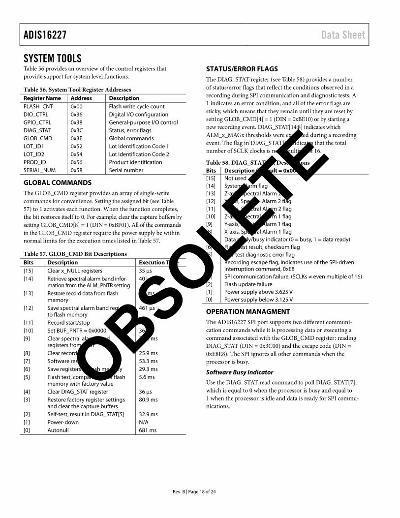
SYSTEM TOOLS Table 56 provides an overview of the control registers that provide support for system level functions.
Table 56. System Tool Register Addresses Register Name Address Description FLASH_CNT 0x00 Flash write cycle count DIO_CTRL 0x36 Digital I/O configuration GPIO_CTRL 0x38 General-purpose I/O control DIAG_STAT 0x3C Status, error flags GLOB_CMD 0x3E Global commands LOT_ID1 0x52 Lot Identification Code 1 LOT_ID2 0x54 Lot Identification Code 2 PROD_ID 0x56 Product identification SERIAL_NUM 0x58 Serial number
GLOBAL COMMANDS The GLOB_CMD register provides an array of single-write commands for convenience. Setting the assigned bit (see Table 57) to 1 activates each function. When the function completes, the bit restores itself to 0. For example, clear the capture buffers by setting GLOB_CMD[8] = 1 (DIN = 0xBF01). All of the commands in the GLOB_CMD register require the power supply be within normal limits for the execution times listed in Table 57.
Table 57. GLOB_CMD Bit Descriptions Bits Description Execution Time [15] Clear x_NULL registers 35 µs [14] Retrieve spectral alarm band infor-
mation from the ALM_PNTR setting 40 µs
[13] Restore record data from flash memory
1.9 ms
[12] Save spectral alarm band registers to flash memory
461 µs
[11] Record start/stop N/A [10] Set BUF_PNTR = 0x0000 36 µs [9] Clear spectral alarm band
registers from flash 25.8 ms
[8] Clear records 25.9 ms [7] Software reset 53.3 ms [6] Save registers to flash memory 29.3 ms [5] Flash test, compare sum of flash
memory with factory value 5.6 ms
[4] Clear DIAG_STAT register 36 µs [3] Restore factory register settings
and clear the capture buffers 80.9 ms
[2] Self-test, result in DIAG_STAT[5] 32.9 ms [1] Power-down N/A [0] Autonull 681 ms
STATUS/ERROR FLAGS The DIAG_STAT register (see Table 58) provides a number of status/error flags that reflect the conditions observed in a recording during SPI communication and diagnostic tests. A 1 indicates an error condition, and all of the error flags are sticky, which means that they remain until they are reset by setting GLOB_CMD[4] = 1 (DIN = 0xBE10) or by starting a new recording event. DIAG_STAT[14:8] indicates which ALM_x_MAGx thresholds were exceeded during a recording event. The flag in DIAG_STAT[3] indicates that the total number of SCLK clocks is not a multiple of 16.
Table 58. DIAG_STAT Bit Descriptions Bits Description (Default = 0x0000) [15] Not used [14] System alarm flag [13] Z-axis, Spectral Alarm 2 flag [12] Y-axis, Spectral Alarm 2 flag [11] X-axis, Spectral Alarm 2 flag [10] Z-axis, Spectral Alarm 1 flag [9] Y-axis, Spectral Alarm 1 flag [8] X-axis, Spectral Alarm 1 flag [7] Data ready/busy indicator (0 = busy, 1 = data ready) [6] Flash test result, checksum flag [5] Self-test diagnostic error flag [4] Recording escape flag, indicates use of the SPI-driven
interruption command, 0xE8 [3] SPI communication failure, (SCLKs ≠ even multiple of 16) [2] Flash update failure [1] Power supply above 3.625 V [0] Power supply below 3.125 V
OPERATION MANAGMENT The ADIS16227 SPI port supports two different communi-cation commands while it is processing data or executing a command associated with the GLOB_CMD register: reading DIAG_STAT (DIN = 0x3C00) and the escape code (DIN = 0xE8E8). The SPI ignores all other commands when the processor is busy.
Software Busy Indicator
Use the DIAG_STAT read command to poll DIAG_STAT[7], which is equal to 0 when the processor is busy and equal to 1 when the processor is idle and data is ready for SPI commu-nications.
OBSOLETE
Data Sheet ADIS16227
Rev. B | Page 19 of 24
Software Escape Code
The only SPI command available when the processor is busy is the escape code, which is 0xE8E8. Send this command in a repeating pattern, with a small delay between each write cycle, to the DIN pin, while monitoring DIAG_STAT[7]. The follow-ing code example illustrates this process: DIAG_STAT = 0; DIAG_STAT = read_reg(0x3C); while ((DIAG_STAT & 0x0080) == 0) { write_reg(0xE8E8) delay_us(50) DIAG_STAT = read_reg(0x3C) }
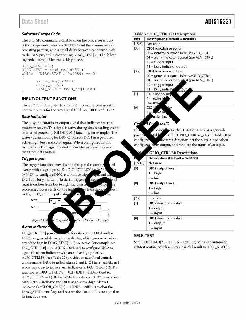
INPUT/OUTPUT FUNCTIONS The DIO_CTRL register (see Table 59) provides configuration control options for the two digital I/O lines, DIO1 and DIO2.
Busy Indicator
The busy indicator is an output signal that indicates internal processor activity. This signal is active during data recording events or internal processing (GLOB_CMD functions, for example). The factory default setting for DIO_CTRL sets DIO1 as a positive, active high, busy indicator signal. When configured in this manner, use this signal to alert the master processor to read data from data buffers.
Trigger Input
The trigger function provides an input pin for starting record events with a signal pulse. Set DIO_CTRL[7:0] = 0x2F (DIN = 0xB62F) to configure DIO2 as a positive trigger input and keep DIO1 as a busy indicator. To start a trigger, the trigger input signal must transition from low to high and then from high to low. The recording process starts on the high-to-low transition, as shown in Figure 17, and the pulse duration must be at least 2.6 µs.
DIO1
DIO2
CAPTURE TIME
ΔtΔt ≥ 2.6µs
0942
5-01
4
Figure 17. Manual Trigger/Busy Indicator Sequence Example
Alarm Indicator
DIO_CTRL[5:2] provide controls for establishing DIO1 and/or DIO2 as a general alarm output indicator, which goes active when any of the flags in DIAG_STAT[13:8] are active. For example, set DIO_CTRL[7:0] = 0x12 (DIN = 0xB612) to configure DIO2 as a generic alarm indicator with an active high polarity. ALM_CTRL[6] (see Table 22) provides an additional control, which enables DIO2 to reflect Alarm 2 and DIO1 to reflect Alarm 1 when they are selected as alarm indicators in DIO_CTRL[5:2]. For example, set DIO_CTRL[7:0] = 0x17 (DIN = 0xB617) and set ALM_CTRL[6] = 1 (DIN = 0xB440) to establish DIO2 as an active-high Alarm 2 indicator and DIO1 as an active-high Alarm 1 indicator. Set GLOB_CMD[4] = 1 (DIN = 0xBE10) to clear the DIAG_STAT error flags and restore the alarm indicator signal to its inactive state.
Table 59. DIO_CTRL Bit Descriptions Bits Description (Default = 0x000F) [15:6] Not used [5:4] DIO2 function selection 00 = general-purpose I/O (use GPIO_CTRL) 01 = alarm indicator output (per ALM_CTRL) 10 = trigger input 11 = busy indicator output [3:2] DIO1 function selection 00 = general-purpose I/O (use GPIO_CTRL) 01 = alarm indicator output (per ALM_CTRL) 10 = trigger input 11 = busy indicator output [1] DIO2 line polarity 1 = active high 0 = active low [0] DIO1 line polarity 1 = active high 0 = active low
General-Purpose I/O
If DIO_CTRL configures either DIO1 or DIO2 as a general-purpose digital line, use the GPIO_CTRL register in Table 60 to configure its input/output direction, set the output level when configured as an output, and monitor the status of an input.
Table 60. GPIO_CTRL Bit Descriptions Bits Description (Default = 0x0000) [15:10] Not used [9] DIO2 output level 1 = high 0 = low [8] DIO1 output level 1 = high 0 = low [7:2] Reserved [1] DIO2 direction control 1 = output 0 = input [0] DIO1 direction control 1 = output 0 = input
SELF-TEST Set GLOB_CMD[2] = 1 (DIN = 0xBE02) to run an automatic self-test routine, which reports a pass/fail result to DIAG_STAT[5].
OBSOLETE

ADIS16227 Data Sheet
Rev. B | Page 20 of 24
FLASH MEMORY MANAGEMENT Set GLOB_CMD[5] = 1 (DIN = 0xBE20) to run an internal checksum test on the flash memory, which reports a pass/fail result to DIAG_STAT[6]. The FLASH_CNT register (see Table 61) provides a running count of flash memory write cycles. This is a tool for managing the endurance of the flash memory. Figure 18 quantifies the relationship between data retention and junction temperature.
Table 61. FLASH_CNT Bit Descriptions Bits Description [15:0] Binary counter for writing to flash memory
600
450
300
150
030 40
RET
ENTI
ON
(Yea
rs)
JUNCTION TEMPERATURE (°C)55 70 85 100 125 135 150
0942
5-01
5
Figure 18. Flash/EE Memory Data Retention
DEVICE IDENTIFICATION
Table 62. LOT_ID1 and LOT_ID2 Bit Descriptions Bits Description [15:0] Lot identification code
Table 63. PROD_ID Bit Descriptions Bits Description [15:0] 0x3F63 = 16,227
Table 64. SERIAL_NUM Bit Descriptions Bits Description [15:0] Serial number, lot specific
OBSOLETE

Data Sheet ADIS16227
Rev. B | Page 21 of 24
APPLICATIONS INFORMATION MOUNTING GUIDELINES The ADIS16227 provides a threaded hole for a 10-32 UNF machine screw. This hole is 9 mm deep, and the tapped depth is 7 mm. Use a torque of 15 inch-pounds when tightening the 10-32 mounting fastener and make sure that the fastener doesn’t bottom-out in the ADIS16227 when tightening.
GETTING STARTED When the power supply voltage of the ADIS16227 reaches 3.15 V, it executes a start-up sequence that places the device in manual FFT mode. The following code example initiates a manual data recording by setting GLOB_CMD[11] = 1 (DIN = 0xBF08) and reads all 256 samples in the x-axis acceleration buffer, using DIN = 0x1400. The data from the first spi_reg_read is not valid because this command starts the process. The second spi_reg_read command (the first read inside the embedded for loop) produces the first valid data. This code sequence produces CS, SCLK, and DIN signals similar to the ones shown in Figure 11.
spi_write(BF08h);
delay 30ms;
Data(0) = spi_reg_read(14h);
For n = 0 to 255
Data(n) = spi_reg_read(14h);
n = n + 1;
end
INTERFACE BOARD The ADIS16227/PCBZ provides the ADIS16227 on a small printed circuit board (PCB) that simplifies the connection to an existing processor system. A single 10-32 machine screw (Fastener Express, FHS1106-4I2) secures the ADIS16227CMLZ to the interface board. The first set of mounting holes on the interface boards is in the four corners of the PCB and provides clearance for 4-40 machine screws. The second set of mounting holes provides a pattern that matches the ADISUSBZ evaluation system, using M2 × 0.4 mm machine screws. These boards are made of IS410 material and are 0.063 inches thick. The J1 connector uses Pin 1 through Pin 12 in this pattern. Pin 13 and Pin 14 are for future expansion, but they also provide convenient probe points for the
DIO1 and DIO2 signals. The connector is a dual row, 2 mm (pitch) connector that works with a number of ribbon cable systems, including 3M Part Number 152212-0100-GB (ribbon-crimp connector) and 3M Part Number 3625/12 (ribbon cable). The LEDs (D1 and D2) provide visual indication of the DIO1 and DIO2 signals.
0942
5-01
7
Figure 19. Electrical Schematic
0942
5-01
8
Figure 20. PCB Assembly View and Dimensions
OBSOLETE

ADIS16227 Data Sheet
Rev. B | Page 22 of 24
OUTLINE DIMENSIONS
06-2
1-20
10-A
15.2015.00 SQ14.80
TOP VIEW
6.00BCS1.00 BSC
PITCH
3.88 NOM
0.45 NOM
0.50 BCS
DETAIL A
BOTTOM VIEW
17.50 NOM
DETAIL A
SIDE VIEWFRONT VIEW
15.2015.0014.80 4.20
4.104.00
9.209.008.80
0.54NOM
Ø 4.04 910-32 UNF 7
Ø 6.10 90°,NEAR SIDE
Figure 21. 14-Lead Module with Connector Interface
(ML-14-2) Dimensions shown in millimeters
ORDERING GUIDE Model1 Temperature Range Package Description Package Option ADIS16227CMLZ −40°C to +125°C 14-Lead Module with Connector Interface ML-14-2 ADIS16227/PCBZ Evaluation Board 1 Z = RoHS Compliant Part.
OBSOLETE

Data Sheet ADIS16227
Rev. B | Page 23 of 24
NOTES
OBSOLETE

ADIS16227 Data Sheet
Rev. B | Page 24 of 24
NOTES
©2010–2012 Analog Devices, Inc. All rights reserved. Trademarks and registered trademarks are the property of their respective owners. D09425-0-5/12(B)
OBSOLETE