Embed Size (px)
Citation preview

High-temp plasma doping using PULSION tool : A development allowed by SEAL European project F. Milesi1; F.Torregrosa²; J. Duchaine²; F.Mazen1; S. Reboh1; N. Payen1
1 - CEA-LETI 2 – Ion Beam Services
High-temp plasma doping using PULSION tool : A development allowed by SEAL European project
• Introduction – Objectives of SEAL Project – Implant technology evolution with a comparison PIII vs BLII
•Pulsion® presentation & tool evolution
•Results with Arsenic ion implantation at high temperature
•Conclusion – Electric results on advanced devices
High-temp plasma doping using PULSION tool : A development allowed by SEAL European project
• Introduction
•Pulsion® presentation & tool evolution
•Results with Arsenic ion implantation with
temperature
•Conclusion
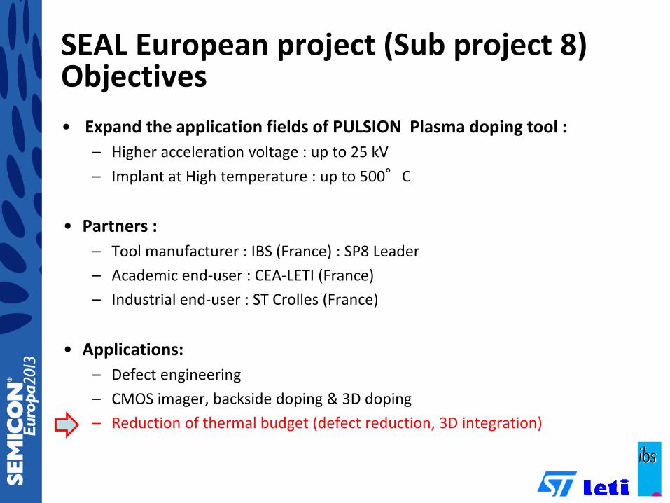
SEAL European project (Sub project 8) Objectives • Expand the application fields of PULSION Plasma doping tool :
– Higher acceleration voltage : up to 25 kV – Implant at High temperature : up to 500°C
• Partners :
– Tool manufacturer : IBS (France) : SP8 Leader – Academic end-user : CEA-LETI (France) – Industrial end-user : ST Crolles (France)
• Applications:
– Defect engineering – CMOS imager, backside doping & 3D doping – Reduction of thermal budget (defect reduction, 3D integration)

Introduction
28nm 20nm 14nm 11nm 8nm
Planar FD-SOI Double Gate Tri Gate (Lg~H) / FinFET (H>>Lg) Nano Wire
•Evolution of devices structure leads a transition from a planar to 3D architecture • Evolution of doping process
– Use thin films on insulator (SOI with Si Top<10nm) – Conformal doping (side wall) – Crystallinity control (damage vs amorphization)
Evolution of MOS transistors architecture as function of nodes technology 3D Monolithic transistors

Introduction
•The evolution of doping process leads in the evolution of ion implantation technology
•Beam Line Ion Implanter – Medium current - Very low energy – High current - High dose (higher throughput) – High energy
• Plasma Immersion Ion Implanter

Introduction
• Beam Line – One specy – One energy – Gaussian profile – Rp concentration max – Uni-directional
• Plasma Immersion – Multi-species – Multi-energies – Decreasing linear profile – Surface concentration max – Multi-directionals
High-temp plasma doping using PULSION tool : A development allowed by SEAL European project
• Introduction
•Pulsion® presentation & tool evolution
•Results with Arsenic ion implantation with
temperature
•Conclusion

PULSION Plasma Doping Tools • From Laboratories to High Volume Production • For 3D doping, Low Energy & High dose implant (Contact, DPG), Material
Modification
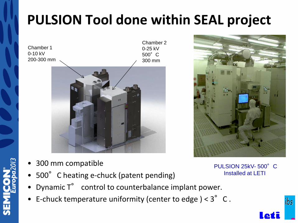
PULSION Tool done within SEAL project
• 300 mm compatible • 500°C heating e-chuck (patent pending) • Dynamic T° control to counterbalance implant power. • E-chuck temperature uniformity (center to edge ) < 3°C .
Chamber 1 0-10 kV 200-300 mm
Chamber 2 0-25 kV 500°C 300 mm
PULSION 25kV- 500°C Installed at LETI
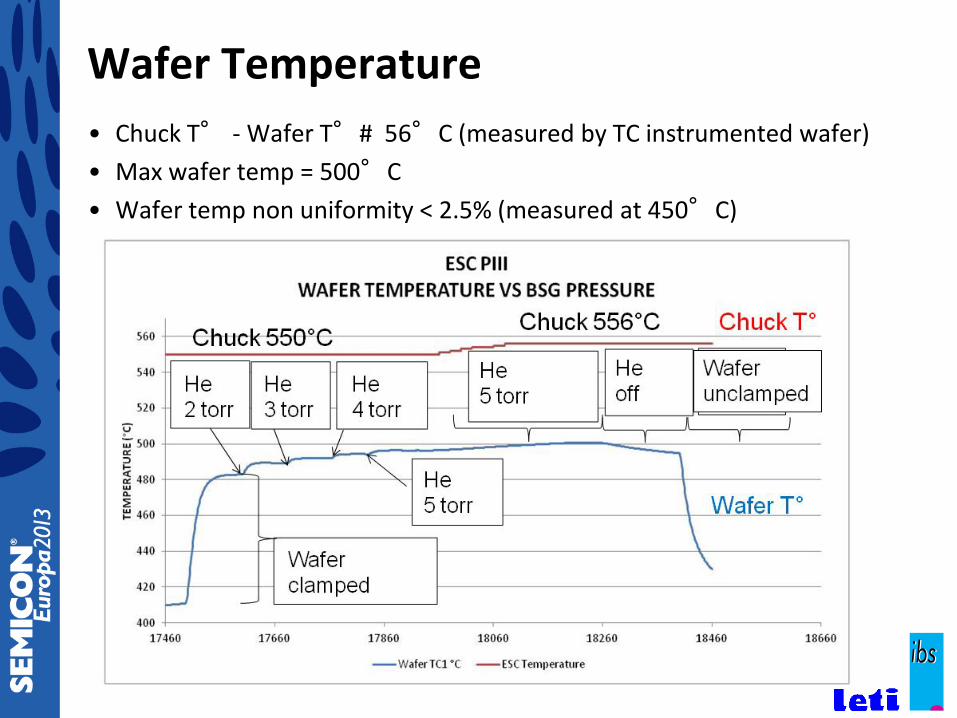
Wafer Temperature • Chuck T° - Wafer T°# 56°C (measured by TC instrumented wafer) • Max wafer temp = 500°C • Wafer temp non uniformity < 2.5% (measured at 450°C)

High-temp plasma doping using PULSION tool : A development allowed by SEAL European project
• Introduction
•Pulsion® presentation & tool evolution
•Results with Arsenic ion implantation with
temperature
•Conclusion

Arsenic ion implantation at high temp. • AsH3 9kV ion implantation in Pulsion tool with different conditions :
– Various doses from 1E14 to 1E16 at/cm² – With & without post-implant anneal (1050°C Spike Anneal ) – Wafer temperature from Room Temperature to 500°C
Dopant activation during ion implantation with wafer temperature Interest for a thermal budget diminution for dopant activation
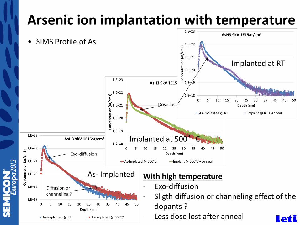
Arsenic ion implantation with temperature • SIMS Profile of As
With high temperature - Exo-diffusion - Sligth diffusion or channeling effect of the
dopants ? - Less dose lost after anneal
Exo-diffusion
Diffusion or channeling ?
Dose lost
As- Implanted
Implanted at 500°C
Implanted at RT
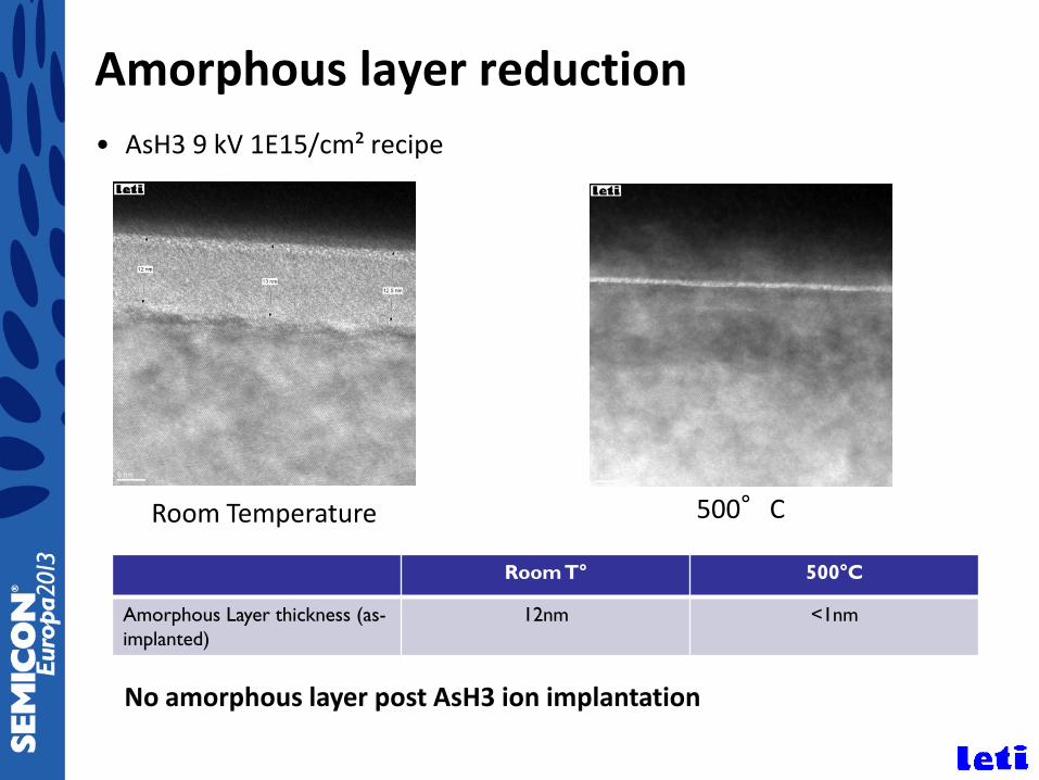
Amorphous layer reduction • AsH3 9 kV 1E15/cm² recipe
No amorphous layer post AsH3 ion implantation
Room Temperature 500°C
Room T° 500°C
Amorphous Layer thickness (as-implanted)
12nm <1nm
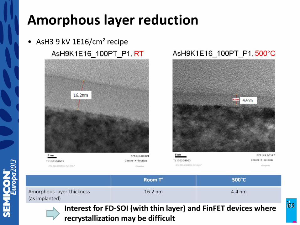
Amorphous layer reduction • AsH3 9 kV 1E16/cm² recipe
Interest for FD-SOI (with thin layer) and FinFET devices where recrystallization may be difficult

High-temp plasma doping using PULSION tool : A development allowed by SEAL European project
• Introduction
•Pulsion® presentation & tool evolution
•Results with Arsenic ion implantation with
temperature
•Conclusion
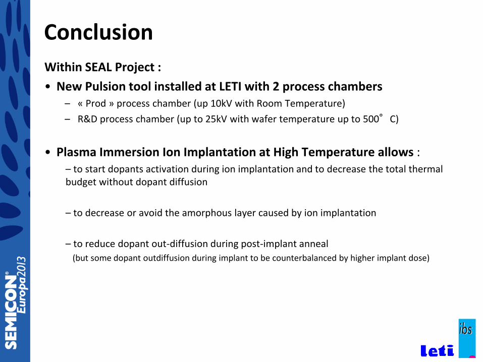
Conclusion Within SEAL Project : • New Pulsion tool installed at LETI with 2 process chambers
– « Prod » process chamber (up 10kV with Room Temperature) – R&D process chamber (up to 25kV with wafer temperature up to 500°C)
• Plasma Immersion Ion Implantation at High Temperature allows : – to start dopants activation during ion implantation and to decrease the total thermal budget without dopant diffusion – to decrease or avoid the amorphous layer caused by ion implantation – to reduce dopant out-diffusion during post-implant anneal
(but some dopant outdiffusion during implant to be counterbalanced by higher implant dose)

Conclusion • Introduction PIII process in the CMOS flow chart for LDD Ion
Implantation – Tri-Gate devices – Very small devices ==> the electrical performance depending of the transistor dimensions
Schema of a Tri-Gate transistor Lg (< 20nm) ~ H (12nm)
Ion / Ioff clouds of devices for both NMOS and PMOS The Ion extraction is made at Vg=Vd=0.9V
• For the same Ioff, Ion +11% @ NMOS & +18% @ PMOS
Plasma Immersion Ion Implantation For Sub 22nm Node Devices: FD-SOI and Trigate Nano-Wire; F. Milesi & al.; IIT2012 @ Valladolid
Conclusion Plasma Immersion Ion Implantation vs Beam Line Ion Implantation • From the device efficiency point of view, need of PIII depends on device
structure : – PIII is more efficient than Beam Line for 3D structure – Explained by a best access resistance and a good electrostatic gate control of the
channel caused by conformal Implant
Plasma Immersion Ion Implantation For Sub 22nm Node Devices: FD-SOI and Trigate Nano-Wire; F. Milesi & al.; IIT2012 @ Valladolid
Contacts F. Milesi , CEA-LETI : [email protected] F. Torregrosa, IBS : [email protected] SEAL Project
Information and Acknowledgement
Thank you!