Embed Size (px)
Citation preview
Progress In Electromagnetics Research C, Vol. 31, 41–52, 2012
HIGH PERFORMANCE V-BAND GAAS LOW NOISEAMPLIFIER WITH MODIFIED COPLANAR WAVEG-UIDE EBG TRANSMISSION LINES TECHNOLOGY
P.-Y. Ke, F.-H. Huang, and H.-C. Chiu*
Department of Electronics Engineering, Chang Gung University, Tao-Yuan 259, Taiwan
Abstract—This paper presents an integrated millimeter-wave(mmW) low noise amplifier (LNA) which is implemented by using0.15-µm baseline GaAs pHEMT technology. The design utilized mod-ified co-planar waveguide (CPW) to perform a slow wave transmissionline (TLine) with electromagnetic band gap (EBG) ground structuresfor the input/output matching networks. The low noise V-band LNAchip size was hence reduced by adopting the new EBG transmissionlines. The developed amplifier exhibited a noise figure of 6.21 dB, anda peak gain of 17.3 dB at 66GHz. Additionally, the amplifier has linearcharacteristics and its measured third-order intercept (IIP3) point isgreater than −0.5 dBm under a dc power consumption of 75mW.
1. INTRODUCTION
Recently, high data rate requirements has grown a fast interest in theunlicensed band, the wide available bandwidth of 7 GHz (57–64 GHzin the USA, 59–66 GHz in Japan, 57–66 GHz in Europe) fueled bystandards and applications led by WiHD, WiGig and 802.15c. Interestin IEEE 802.15c communications systems for indoor and high speedwireless application has led to significant progress of broadband mmWintegrated circuits and wireless personal area networks (WPAN) aimto deliver data rates of 2 to 3Gb/s or even more. GaAs technologyprovides a low loss substrate, a high linear output power and a lowsignal distortion compared to traditional RFCMOS process. In thispaper, we describe a compact size and a high performance V-bandGaAs pHEMT LNA by using EBG ground structure.
Impedance matching networks in the reported circuits were basedupon either lumped inductors [1] or electromagnetic bandgap (EBG)
Received 29 April 2012, Accepted 1 July 2012, Scheduled 4 July 2012* Corresponding author: Hsien-Chin Chiu ([email protected]).

42 Ke, Huang, and Chiu
structures CPW TLines [2, 3]. Lumped inductors offer smaller areaand larger quality factors than TLine based matching networks, butare more difficult to be precisely simulated at millimeter-wave band.Modified CPW for EBG-CPW TLines, on the other hand, can beconsiderably smaller than their conventional counterparts and exhibithigh Q values [1, 4, 5].
In this work, a compact size V-band LNA with EBG TLines wasdemonstrated in standard 0.15-µm GaAs pHEMT process for low noisesolution. As an important component for most receivers, the LNA wasdesigned to provide low noise figure and to obtain respectable gain overa broad frequency band especially for high data rate application. Theproposed LNA is designed to simultaneously achieve high gain and lownoise characteristics.
2. INTERCONNECTION EBG-CPW TLINES
The values of the required inductances in the circuit are smaller thanthose provided by standard spiral inductors and we have thereforeopted for the TLine approach. Conventional coplanar microstrip, andgrounded microstrip TLines on GaAs substrate typically exhibitedquality factor of 10∼25, which are not sufficient for low noise design.Since it has been shown that EBG TLines can provide much higherQ values [2], we have also taken this approach into this study. Thestructure of the EBG TLines used in this work is shown in Fig. 1.The slotted bottom metallic shields were patterned as 130µm metalstripes separated by 10µm slot widths. The signal line metal widthwas 37µm, the distance between signal line metal and the metallicground was 5µm. All metal layer resistivity was 0.02 ohm/square, andinsulator layers GaAs.
The electromagnetic simulation of EBG TLines is fairly complex,but can be preformed successfully. The numerical analysis of theEBG-CPW LNA studied is performed using the commercial computersoftware package, Momentum of Agilent Technologies, AdvancedDesign System (ADS), which is based on the method of moment(MoM) technique for layered media. Momentum solves mixed potentialintegral equations (MPIE) using full wave Green’s functions.
A comparison of the standard (Std.) CPW TLine and EBG-CPWTLines, simulated performance of the TLines is shown in Fig. 2(a).high Q values obtained. For comparison purposes, the results of aclassical CPW TLine realized. The centre cut-off frequency which isthe resonant frequency depends on the transverse slots number and thesquare etched hole of the ground plane. The geometrical dimensionsand the 60-GHz main electrical properties are summarized in Table 1.

Progress In Electromagnetics Research C, Vol. 31, 2012 43
Figure 1. EBG TLine with slotted ground shield.
30 40 50 60 70 80 90 100 110 120 1300
10
20
30
40
50
60
70
80
90
Frequency [GHz]
Qu
ali
ty F
act
or
EBG-CPW3
EBG-CPW2
EBG-CPW1
Std. CPW
54 55 56 57 58 59 6073.0
73.5
74.0
74.5
Frequency [GHz]
(a) (b)L-TLine
G W
SL SS
Figure 2. (a) Simulated quality factor. (b) Cross-section of the EBGCPW topology.
In order to avoid the complex EM simulations of EBG CPWTLines, we have developed a simple analytic model, which accuratelypredicts their properties. The model takes advantage of the wellestablished models of grounded and standard CPWs. The Z element(L, R and C) of EBG TLine model is shown in Fig. 3. It shows thatEBG TLine obtained high quality factor (large propagation constant)

44 Ke, Huang, and Chiu
Table 1. Physical characteristics and 60-GHz electrical properties forDGS S-CPW.
Parameters
S-CPW parameters Electrical
performance at 60 GHz 1
W ( m)
G
Slot number
SS
SL
L
Wg
TLinelength
Z )( Q
Std.CPW TLine
42 7 − − 250 450 50.7 73.6
EBG
S-CPW1 37 5 9 5 15 130 250 450 49.5 73.8
EBGS-CPW2
37 5 9 10 10 130 250 450 52.4 84.5
EBGS-CPW3
37 5 9 15 5 130 250 450 51.3 79.4
µ Ω( m)µ ( m)µ ( m)µ ( m)µ( m)µ
− −
( m)
µ
can be achieved by increasing C and L in the TLine.The resonant frequency of the parallel circuit is defined as
ω0 =1√LC
(1)
The equivalent impedance equation of the single resonant modelmay be expressed as
Z =1
1R
1jωL + jωC
(2)
According to the microwave network theory as
S21 =2Z0
2Z0 + Z=
2Z0
2Z0 + 11/R+1/jωL+jωC
(3)
The 3-dB cut-off angular frequency ωc can be determined as
S21 =2Z0
2Z20 +
(ωc/C
ω20−ω2
c
)2 =1√2, R À Z0 (4)
(1) Into (3), the Capacitance is obtained as
C =ωc
2Z0
(ω2
0 − ω2c
) (5)
The inductance can be determined by
L =1
ω20C
14π2f2
0 C(6)

Progress In Electromagnetics Research C, Vol. 31, 2012 45
Zo Zo
Z
Gnd
L
C
R
Figure 3. EBG TLine model.
30 40 50 60 70 80 90
-25
-20
-15
-10
-5
0
Frequency(GHz)
S21 (
dB
)
EM-Simulation data Circuit-Simulaion data
Figure 4. EM simulated dataand circuit simulation data.
Table 2. Parameters extracted from equivalent circuit.
Parameters Parameters valueSlot, D (µm) 10
Signal width, W (µm) 37Metallic ground, G (µm) 5
Resonant frequency, ωo (GHz) 60Inductance, L (nH) 0.011Capacitance, C (pF) 0.64Resistance, R1 (kΩ) 1.49
Therefore, the resistance R of the circuit can be obtained formresonant frequency ω respectively
S21 |ω=ω0=
∣∣∣∣2Z0
2Z0 + Zs
∣∣∣∣ =2Z0
2Z0 + R⇒ R = 2Z0
1− S21 |ω=ω0
S21 |ω=ω0
(7)
Therefore, this model can predict the EBG TLines with slottedground shield over the relatively wider frequency range from 50 to70GHz, as shown in Fig. 1, in which the circuit simulation results andthe EM simulation results show good agreement, as shown in Fig. 4.The resistors, capacitances and inductances are evaluated from theresonant frequencies of the EBG TLines with slotted ground shieldand listed in Table 2.

46 Ke, Huang, and Chiu
3. V-BAND LNA DESIGN
The proposed LNA was demonstrated on 6 inch semi-insulating GaAspseudomorphic high electron mobility transistor (pHEMT) technologytogether with a 0.15µm gate length T-gate technology which wasdirectly written by electron beam writer. A 12 nm undoped InGaAschannel layer was sandwiched between two Si planar δ-doped layersfor high current and high power consideration. A 25 nm-thick n+
AlGaAs (1×1017cm−3) layer was grown on an intrinsic AlGaAs spacerlayer as a Schottky layer, which improves parallel conduction at highvoltage. Finally, a 35 nm n+-GaAs cap layer was grown to improvethe resistivities of the ohmic contacts. Ohmic contacts were realizedby using Au/Ge/Ni/Au alloy followed by a 430C, 15 seconds rapidthermal annealing (RTA) alloy. Ion-implant isolation technology wasused for mesa isolation to prevent the flow of any side-wall gate leakagecurrent. The 0.15µm-long T-shaped photoresist profile was formed bybi-layer polymer design and electron beam directly writing technology.After the highly selective succinic acid chemical gate recess process,the Ti/Pt/Au-gates were deposited by lift-off process. Before thedeposition of metal-1, a 1000 A SiNx was deposited by plasma enhancechemical vapor deposition (PECVD) at 280C for passivation. The1µm A-thick gold metal (Ti/Au = 500 A/10000 A) was then depositedon the SiNx passivation layer using an electron-beam evaporator.Finally, a 2000 A SiNx layer was deposited as a insulator layer betweenmetal-1 layer and metal-2 layer (2µm-thick gold). The pHEMT of 2fingers with total gate width of 50µm has a typical unit current gaincutoff frequency of 78 GHz, power gain cut-off frequency of 134GHzwith 3 V supply.
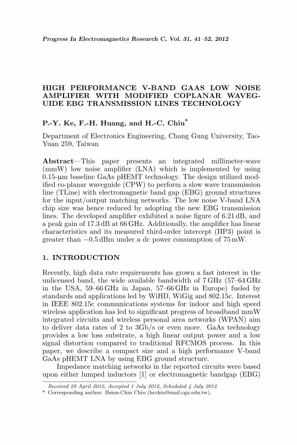
The three stage common-source LNA schematics are shown inFig. 5. The first stage transistor had 2 fingers with total gatewidth of 50µm. It was biased at a supply voltage of 3 V and draincurrent of 13 mA. Note that all the matching networks and inductancesincorporate EBG-CPW slow wave transmission lines.
The contribution of each noise source to the total output noise isevaluated. The NF is then calculated by evaluating the ratio of thetotal output noise to the output noise due to parasitic resistance andtransistor source resistance.
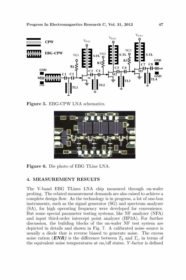
A die photo is shown in Fig. 6. Note in particular that the EBGTLines are much shorter (by a factor of two) than similar designs usingconventional TLines. The chip size of 1.2× 0.8mm2.
Progress In Electromagnetics Research C, Vol. 31, 2012 47
C1 C2
C3 C4
C5 C6
C7 C8
VG1VG2
VG3
VD D1
VD D2
VD D 3
R1
R2R3
RFin
RFoutGND
GND
GND
GNDM1
M2
M3
TL1TL2
TL4TL3
S-TLS -TL S -TL
CPW
EBG-CPW
Figure 5. EBG-CPW LNA schematics.
Figure 6. Die photo of EBG TLine LNA.
4. MEASUREMENT RESULTS
The V-band EBG TLines LNA chip measured through on-waferprobing. The related measurement demands are also raised to achieve acomplete design flow. As the technology is in progress, a lot of one-boxinstruments, such as the signal generator (SG) and spectrum analyzer(SA), for high operating frequency were developed for convenience.But some special parameter testing systems, like NF analyzer (NFA)and input third-order intercept point analyzer (IIP3A). For furtherdiscussion, the building blocks of the on-wafer NF test system aredepicted in details and shown in Fig. 7. A calibrated noise source isusually a diode that is reverse biased to generate noise. The excessnoise ration (ENR) is the difference between Th and Tc, in terms ofthe equivalent noise temperatures at on/off states. Y -factor is defined

48 Ke, Huang, and Chiu
Agilent 347BNoise source50-75 GHz
DUT
Agilent 11974 V
Down-converter
Agilent E4440A
Series Spectrum Analyzers
Agilent 8490D Attenuator
BPF MIXER IF AMP
LO
Cascade infinity probe
(110 GHz)
1.85 mm adaptor
WR-15 to 1.85 mm adaptor
3.5 mm Cable
1.85 mm Cable
3.5 mm adaptor
WR-15 adaptor
Figure 7. Test setup and procedure of MMW amplifier NFmeasurement.
as the ratio of Nh to Nc which corresponds to the measured noisepowers at on/off states, respectively. A noise source with appropriateENR is essential, as a rule of thumb, it is recommended to choosea higher ENR for high NF DUT or lower ENR for low NF DUT. Ifthe NF of DUT is much higher than the ENR, it will lead to errors.To calculate the Y -factor substituted by ENR and noise factor, thefollowing equations are used [6].
F =Tc + Te
Tc(8)
ENR =Th + Tc
Tc(9)
Y =Th + Te
Tc + Te(10)
where Te is the equivalent noise temperature of DUT. While Y -factor approaches to one, it makes the measured values of the on/offstates too hard to distinguish the DUT’s NF from the self-generatednoise. Whereas the available gain obtained simultaneously in Y -factormethod is derived as below
Ga =Nh DUT−Nc DUTTh DUT−Tc DUT
Nh NFtest system−Nc NFtest system
Th NFtest system−Tc NFtest system
(11)
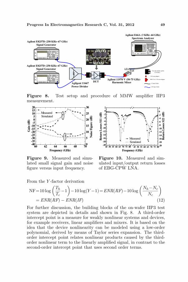
Progress In Electromagnetics Research C, Vol. 31, 2012 49
Agilgent 11667
Power Divider
DUTAgilent 11970 V (50-75 GHz)
Harmonic Mixer
Agilent E8257D (250 KHz~67 GHz)
Signal Generator
Agilent E8257D (250 KHz~67 GHz)
Signal Generator
Agilent E66A (3 KHz~44 GHz)
Spectrum Analyzer
Cascade infinity probe
(110 GHz)
1.85 mm adaptor
WR-15 to 1.85 mm adaptor
3.5 mm Cable
1.85 mm Cable
Figure 8. Test setup and procedure of MMW amplifier IIP3measurement.
60 62 64 66 68 70-40-35-30-25-20-15-10-505
101520
0
5
10
15
20
25
30
Nois
e F
igu
re (
dB
)
Gain
(d
B)
Frequency (GHz)
Measured
Simulated
Figure 9. Measured and simu-lated small signal gain and noisefigure versus input frequency.
45 50 55 60 65 70 75 80-20
-18
-16
-14
-12
-10
-8
-6
-4
-2
0
2
Frequency (GHz)
45 50 55 60 65 70 75 80-20
-18
-16
-14
-12
-10
-8
-6
-4
-2
0
2
Measured
Simulated
Ret
urn
Loss
es S
22 (
dB
)
Ret
urn
Loss
es S
11 (
dB
)
Figure 10. Measured and sim-ulated input/output return lossesof EBG-CPW LNA.
From the Y -factor derivation
NF=10 log(
Th
Tc−1
)−10 log(Y −1)=ENR(RF)−10 log
(Nh−Nc
Nc
)
= ENR(RF)− ENR(IF) (12)
For further discussion, the building blocks of the on-wafer IIP3 testsystem are depicted in details and shown in Fig. 8. A third-orderintercept point is a measure for weakly nonlinear systems and devices,for example receivers, linear amplifiers and mixers. It is based on theidea that the device nonlinearity can be modeled using a low-orderpolynomial, derived by means of Taylor series expansion. The third-order intercept point relates nonlinear products caused by the third-order nonlinear term to the linearly amplified signal, in contrast to thesecond-order intercept point that uses second order terms.

50 Ke, Huang, and Chiu
-40 -30 -20 -10 0 10
0
2
4
6
8
10
12
14
16
18
20
Ou
tpu
t p
ow
er (
dB
m)
Input power (dBm)
Gain
(d
B)
-25
-20
-15
-10
-5
0
5
10
Figure 11. Measured 1 dB powergain compression point.
-40 -35 -30 -25 -20 -15 -10 -5 0 5 10-35
-30
-25
-20
-15
-10
-5
0
5
10
15
20
Ou
tpu
t (d
Bm
)
Input power (dBm)
Figure 12. Measured third-orderinterception point.
Table 3. Comparison table of various V-band LNAs.
Process Freq. (GHz) Peak Gain (dB) NF (dB) PDC (mW) /VDD IIP3 (dBm) Size (mm2)
[7] CMOS 90 nm 64 15.5 6.5 86 NA 0.52
[8] CMOS 65 nm 60 11.5 5.6 72 NA 0.601
[9] CMOS 90 nm 60 13 7 42 NA 0.315
[10] CMOS130 nm 60 12 8.8 54 NA 1.43
[11] GaAs150 nm 60 14 5 NA NA 0. 9
[12] GaAs HBT 60 25 5.8 NA NA 1. 6
[13] GaAs 130 nm 60 14 6 NA NA 0.85
[14] GaAs 150 nm 24.5 20 3.5 106 NA 1
[15] GaAs 200 nm 2.4 15 .1 3.8 NA −3 3
This work 66 17 .3 6.3 75 −0.51 0.96
The V-band EBG TLines LNA chip measured through on-waferprobing. Fig. 9 shows the measured and simulated small signalgain and noise figure versus input frequency from 60 to 70GHz at3V drain bias with total current of 27mA. The related stability K-factor is greater than 1. Fig. 10 shows the measured and simulatedinput/output retune losses of EBG-CPW LNA. The measured smallsignal gain has an amplifier peak gain of 17.3 dB at 66GHz. Theminimum input and output return losses are −16 dB and −18 dB,respectively. The noise figure at the same bias condition exhibits aminimum of 6.21 dB at 66 GHz. The 1-dB power gain compressionpoint and third-order interception point at 66GHz are measured andplotted in Figs. 11 and 12, respectively. The measured output 1-dB compression point of the amplifier is 0.6 dBm and input IP3 is−0.5 dBm at 60 GHz. The total dc power consumption is 75.2 mW.
The performance of the reported LNA is compared to that of the

Progress In Electromagnetics Research C, Vol. 31, 2012 51
similar LNAs in Table 3. Note the lower power consumption and lowernoise figure of the reported circuit compared to the V-Band. In spiteof the TL matching network used in our chip its size is comparable tocircuits using lumped inductor based matching networks.
5. CONCLUSION
A high performance and a compact size V-band LNA was implementedin 0.15-µm baseline GaAs pHEMT process. It exhibited a gain of17.3 dB and noise figure of 6.21 dB at 66GHz operation, and the dcpower consumption is only 75 mW. The matching networks were basedon high Q EBG TLines. The EBG TLines approach enabled us toimprove the circuit performance of in standard GaAs foundry servicefabrication, and to compete well with similar LNAs fabricated by moreadvanced technologies.
ACKNOWLEDGMENT
This work is financially supported by National Science Council [NSC-100-2221-E-182-009], High Speed Intelligent Communication (HSIC)Research Center and Healthy Aging Research Center (HARC), ChangGung University, Taoyuan, Taiwan.
REFERENCES
1. Gunnarsson, S. E., et al., “60 GHz single-chip front-end MMICsand systems for multi-Gb/s wireless communication,” IEEEJournal of Solid State Circuit, Vol. 42, No. 5, 1143–1157,May 2007.
2. Yang, B., X. F. Jin, X. M. Zhang, H. Chi, and S. L. Zheng“Photonic generation of 60 GHz millimeter-wave by frequencyquadrupling based on a mode-locking SOA fiber ring laser with alow modulation depth MZM,” Journal of Electromagnetic Wavesand Applications, Vol. 24, No. 13, 1773–1782, Jan. 2010
3. Liu, Y., J. Xu, Y.-Y. Wei, X. Xu, F. Shen, M. Huang, T. Tang,W.-X. Wang, Y.-B. Gong, and J. Feng, “Design of a V-band high-power sheet-beam coupled-cavity traveling-wave tube,” ProgressIn Electromagnetics Research, Vol. 123, 31–45, 2012.
4. Chowdhury, D., P. Reynaert, and A. M. Niknejad, “A 60 GHz 1 V+12.3 dBm transformer-coupled wideband PA in 90 nm CMOS,”ISSCC Dig. Tech. Papers, 560–561, Feb. 2008.

52 Ke, Huang, and Chiu
5. Moghadasi, S. M., A. R. Attari, and M. M. Mirsalehi, “Compactand wideband 1-D mushroom-like EBG filters,” Progress InElectromagnetics Research, Vol. 83, 323–333, 2008.
6. Agilent Technologies, “Noise figure measurement accuracy — TheY -factor method,” Application Note 57-2, Mar. 2004.
7. Pellerano, S., et al., “A 64 GHz LNA with 15.5 dB Gain and 6.5 dBin 90 nm CMOS,” IEEE Journal of Solid State Circuit, Vol. 43,No. 7, 1542–1552, Jul. 2008.
8. Varonen, M., M. Karkkainen, and K. A. I. Halonen, “Millimeter-wave amplifiers in 65-nm CMOS,” Eur. Solid-State Circuit Conf.,280–283, Sep. 2007.
9. Lin, J.-J., K.-H. To, B. Brown, D. Hammock, M. Majerus,M. Tutt, and W. M. Huang, “Wideband PA and LNA for 60-GHz radio in 90-nm LP CMOS technology,” Compound Semicond.Integr. Circuits Symp., 1–4, Oct. 2008.
10. Doan, C. H., S. Emami, A. M. Niknejad, and R. W. Brodersen,“Millimeter-wave CMOS design,” IEEE Journal of Solid StateCircuit, Vol. 40, No. 1, 144–155, Jan. 2005.
11. Fujii, K., M. Adamski, P. Bianco, D. Gunyan, J. Hall,R. Kishimura, C. Lesko, M. Schefer, S. Hessel, H. Morkner, andA. Niedzwiecki, “A 60 GHz MMIC chipset for 1-Gbith/s wirelesslinks,” IEEE MTT-S International Microwave Symposium Digest,Vol. 3, 1725–1728, Jun. 2–7, 2002.
12. Handa, S., E. Suematsu, H. Tanaka, Y. Motouchi, M. Yagura,A. Yamada, and H. Sato, “60 GHz-band low noise amplifierand power amplifier using InGaP/GaAs HBT technology,” 25thAnnual Technical Digest IEEE Gallium Arsenide IntegratedCircuit (GaAs IC) Symposium, 227–230, 2003.
13. Onodera, K., S. Sugitani, K. Nishimura, and M. Tokumitsu “V-band monolithic low-noise amplifiers using ion-implanted n+-self-aligned GaAs MESFET’s,” IEEE Microw. Guided Wave Lett.,Vol. 9, No. 4, 148–150, Feb. 1999.
14. Luo, S.-M., R.-Y. Hung, S.-H. Weng, Y.-L. Ye, C.-N. Chuang,C.-H. Lin, and H.-Y. Chang, “24-GHz MMIC developmentusing 0.15-µm GaAs PHEMT process for automotive radarapplications,” IEEE Asia Pacific Microwave Conf., APMC, 2008.
15. Ahsan, N., J. Dabrowski, and A. Ouacha,“A self-tuning techniquefor optimization of dual band LNA,” Proc. of the 1st EuropeanWireless Technology Conf., EuWiT, 2008.


![LOW-NOISE, 1.25 GHz, COOLED, HENT AMPLIFIERlibrary.nrao.edu/public/memos/edtn/EDTN_151.pdf · [5] Manuel Sierra, "15 GHz Cooled GaAs FET Amplifier--Design Background Information,"](https://img.dokumen.tips/doc/110x75/60ee979aa360d31402316a32/low-noise-125-ghz-cooled-hent-5-manuel-sierra-15-ghz-cooled-gaas-fet.jpg)