Embed Size (px)
Citation preview
HCMOS Compatible, High CMR,10 MBd Optocouplers
Technical Data
Features• HCMOS/LSTTL/TTL
Performance Compatible
• 1000 V/µs Minimum
Common Mode Rejection
(CMR) at VCM = 50 V (HCPL-
261A Family) and 15 kV/µs
Minimum CMR at VCM =
1000 V (HCPL-261N Family)
• High Speed: 10 MBd Typical
• AC and DC Performance
Specified over Industrial
Temperature Range -40°C to
+85°C• Available in 8 Pin DIP,
SOIC-8 Packages
• Safety Approval
UL Recognized per UL15773750 V rms for 1 minute and5000 V rms for 1 minute(Option 020)
CSA ApprovedIEC/EN/DIN EN 60747-5-2 Approved with VIORM = 630 V peak for HCPL-261A/ 261N Option 060
Applications• Low Input Current (3.0 mA)
HCMOS Compatible Version
of 6N137 Optocoupler
• Isolated Line Receiver
• Simplex/Multiplex Data
Transmission
• Computer-Peripheral
Interface
• Digital Isolation for A/D,
D/A Conversion
• Switching Power Supplies
• Instrumentation
Input/Output Isolation
• Ground Loop Elimination
• Pulse Transformer
Replacement
DescriptionThe HCPL-261A family of opticallycoupled gates shown on this datasheet provide all the benefits of theindustry standard 6N137 familywith the added benefit of HCMOS
HCPL-261A HCPL-061AHCPL-263A HCPL-063AHCPL-261N HCPL-061NHCPL-263N HCPL-063N
compatible input current. Thisallows direct interface to allcommon circuit topologies withoutadditional LED buffer or drivecomponents. The AlGaAs LEDused allows lower drive currentsand reduces degradation by usingthe latest LED technology. On thesingle channel parts, an enableoutput allows the detector to bestrobed. The output of the detectorIC is an open collector schottky-clamped transistor. The internalshield provides a minimumcommon mode transient immunityof 1000 V/µs for the HCPL-261Afamily and 15000 V/µs for theHCPL-261N family.
The connection of a 0.1 µF bypass capacitor between pins 5 and 8 is required.
Functional Diagram
CAUTION: It is advised that normal static precautions be taken in handling and assembly of this component toprevent damage and/or degradation which may be induced by ESD.
1
2
3
4
8
7
6
5
CATHODE
ANODE
GND
V
VCC
O
1
2
3
4
8
7
6
5ANODE 2
CATHODE 2
CATHODE 1
ANODE 1
GND
V
VCC
O2
VE VO1
HCPL-261A/261NHCPL-061A/061N
HCPL-263A/263NHCPL-063A/063N
NC
NCSHIELD SHIELD
LED
ONOFFONOFFONOFF
ENABLE
HHLL
NCNC
OUTPUT
LHHHLH
TRUTH TABLE(POSITIVE LOGIC)
LED
ONOFF
OUTPUT
LH
TRUTH TABLE(POSITIVE LOGIC)
2
Ordering InformationSpecify Part Number followed by Option Number (if desired).
Example:
HCPL-261A#XXXX020 = 5000 V rms/1 minute UL Rating Option*060 = IEC/EN/DIN EN 60747-5-2 VIORM = 630 Vpeak Option**300 = Gull Wing Surface Mount Option***500 = Tape and Reel Packaging OptionXXXE = Lead Free Option
Option data sheets available. Contact your Agilent sales representative or authorized distributor for information.Remarks: The notation “#” is used for existing products, while (new) products launched since 15th July 2001 and lead free option will use “–”*For HCPL-261A/261N/263A/263N (8-pin DIP products) only.**For HCPL-261A/261N only. Combination of Option 020 and Option 060 is not available.***Gull wing surface mount option applies to through hole parts only.
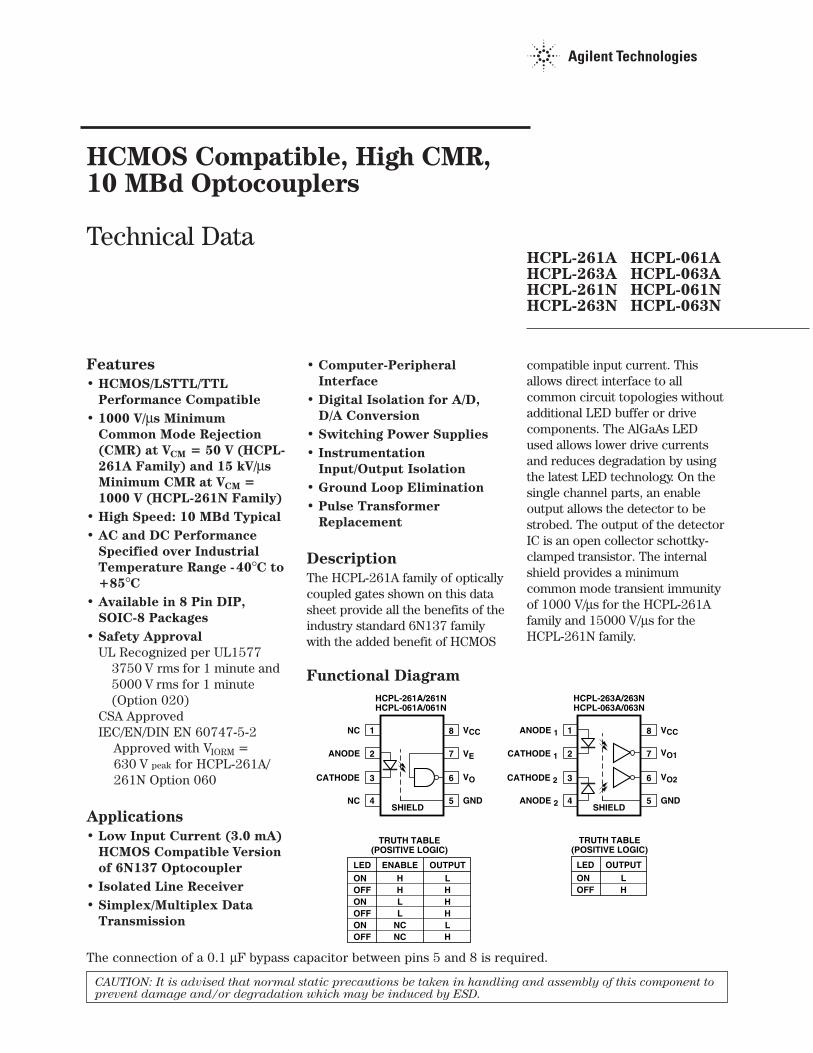
Selection GuideWidebody
Minimum CMR 8-Pin DIP (300 Mil) Small-Outline SO-8 (400 Mil) Hermetic
On- Single Dual Single Dual Single Single and
dV/dt VCM Current Output Channel Channel Channel Channel Channel Dual Channel
(V/µs) (V) (mA) Enable Package Package Package Package Package Packages
NA NA 5 YES 6N137[1] HCPL-0600[1] HCNW137[1]
NO HCPL-2630[1] HCPL-0630[1]
5,000 50 YES HCPL-2601[1] HCPL-0601[1] HCNW2601[1]
NO HCPL-2631[1] HCPL-0631[1]
10,000 1,000 YES HCPL-2611[1] HCPL-0611[1] HCNW2611[1]
NO HCPL-4661[1] HCPL-0661[1]
1,000 50 YES HCPL-2602[1]
3,500 300 YES HCPL-2612[1]
1,000 50 3 YES HCPL-261A HCPL-061A
NO HCPL-263A HCPL-063A
1,000[2] 1,000 YES HCPL-261N HCPL-061N
NO HCPL-263N HCPL-063N
1,000 50 12.5 [3] HCPL-193X[1]
HCPL-56XX[1]
HCPL-66XX[1]
Notes:
1. Technical data are on separate Agilent publications.2. 15 kV/µs with VCM = 1 kV can be achieved using Agilent application circuit.3. Enable is available for single channel products only, except for HCPL-193X devices.
Input
Schematic
SHIELD
8
6
5
2+
3
VF
USE OF A 0.1 µF BYPASS CAPACITOR CONNECTEDBETWEEN PINS 5 AND 8 IS RECOMMENDED (SEE NOTE 16).
–
IF ICC VCC
VO
GND
IO
VE
IE 7
HCPL-261A/261NHCPL-061A/061N
SHIELD
8
7+
2
VF1
–
IF1
ICC VCC
VO1IO1
1
SHIELD
6
5
–
4
VF2
+
IF2
VO2
GND
IO23
HCPL-263A/263NHCPL-063A/063N
3
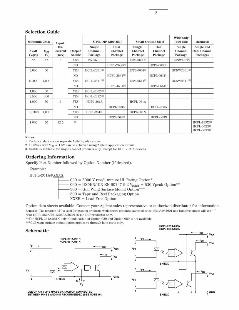
HCPL-261A/261N/263A/263N Outline DrawingPin Location (for reference only)
Figure 2. Gull Wing Surface Mount Option #300.
Figure 1. 8-Pin Dual In-Line Package Device Outline Drawing.
9.40 (0.370)9.90 (0.390)
PIN ONE
1.78 (0.070) MAX.
A XXXXZ
YYWW
OPTION CODE*
DATE CODE
0.76 (0.030)1.40 (0.056)
2.28 (0.090)2.80 (0.110)
0.51 (0.020) MIN.
0.65 (0.025) MAX.
4.70 (0.185) MAX.
2.92 (0.115) MIN.
6.10 (0.240)6.60 (0.260)
0.20 (0.008)0.33 (0.013)
5° TYP.7.36 (0.290)7.88 (0.310)
DIMENSIONS IN MILLIMETERS AND (INCHES).
5678
4321
1.19 (0.047) MAX.
TYPE NUMBER
* MARKING CODE LETTER FOR OPTION NUMBERS."L" = OPTION 020"V" = OPTION 060OPTION NUMBERS 300 AND 500 NOT MARKED.
NOTE: FLOATING LEAD PROTRUSION IS 0.25 mm (10 mils) MAX.
3.56 ± 0.13(0.140 ± 0.005)
0.635 ± 0.25(0.025 ± 0.010)
12° NOM.
9.65 ± 0.25(0.380 ± 0.010)
0.635 ± 0.130(0.025 ± 0.005)
7.62 ± 0.25(0.300 ± 0.010)
5678
4321
9.65 ± 0.25(0.380 ± 0.010)
6.350 ± 0.25(0.250 ± 0.010)
1.02 (0.040)
1.27 (0.050)
10.9 (0.430)
2.0 (0.080)
LAND PATTERN RECOMMENDATION
1.080 ± 0.320(0.043 ± 0.013)
3.56 ± 0.13(0.140 ± 0.005)
1.780(0.070)MAX.1.19
(0.047)MAX.
2.540(0.100)BSC
DIMENSIONS IN MILLIMETERS (INCHES).TOLERANCES (UNLESS OTHERWISE SPECIFIED):
LEAD COPLANARITY MAXIMUM: 0.102 (0.004)
NOTE: FLOATING LEAD PROTRUSION IS 0.25 mm (10 mils) MAX.
xx.xx = 0.01xx.xxx = 0.005
0.20 (0.008)0.33 (0.013)
4
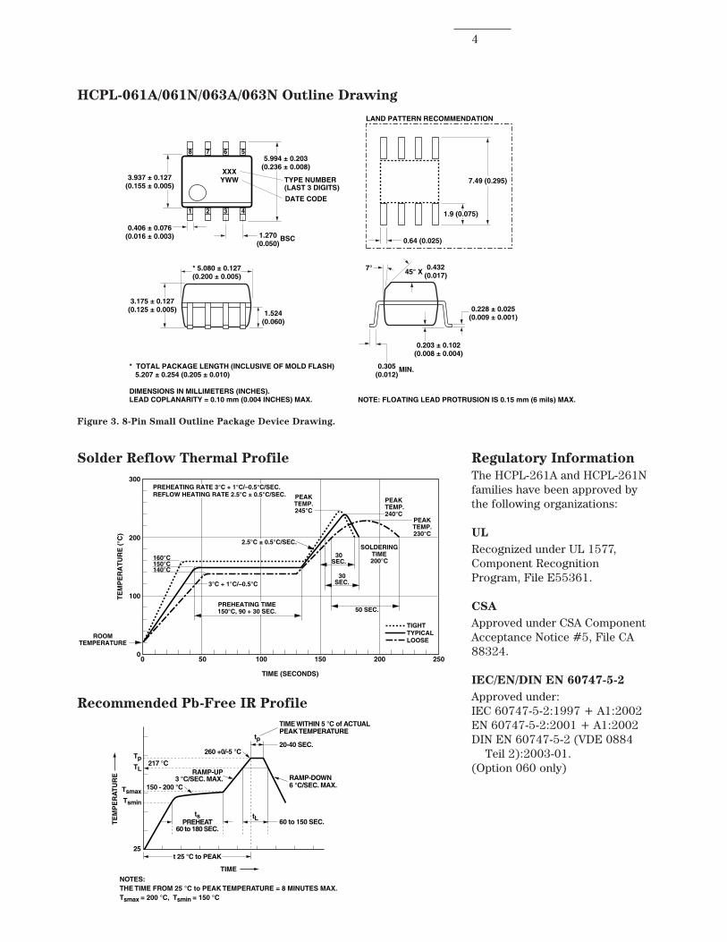
HCPL-061A/061N/063A/063N Outline Drawing
Figure 3. 8-Pin Small Outline Package Device Drawing.
Regulatory InformationThe HCPL-261A and HCPL-261Nfamilies have been approved bythe following organizations:
UL
Recognized under UL 1577,Component RecognitionProgram, File E55361.
CSA
Approved under CSA ComponentAcceptance Notice #5, File CA88324.
IEC/EN/DIN EN 60747-5-2
Approved under:IEC 60747-5-2:1997 + A1:2002EN 60747-5-2:2001 + A1:2002DIN EN 60747-5-2 (VDE 0884 Teil 2):2003-01.(Option 060 only)
XXXYWW
8 7 6 5
4321
5.994 ± 0.203(0.236 ± 0.008)
3.937 ± 0.127(0.155 ± 0.005)
0.406 ± 0.076(0.016 ± 0.003) 1.270
(0.050)BSC
* 5.080 ± 0.127(0.200 ± 0.005)
3.175 ± 0.127(0.125 ± 0.005) 1.524
(0.060)
45° X0.432
(0.017)
0.228 ± 0.025(0.009 ± 0.001)
TYPE NUMBER(LAST 3 DIGITS)
DATE CODE
0.305(0.012)
MIN.* TOTAL PACKAGE LENGTH (INCLUSIVE OF MOLD FLASH) 5.207 ± 0.254 (0.205 ± 0.010)
DIMENSIONS IN MILLIMETERS (INCHES).LEAD COPLANARITY = 0.10 mm (0.004 INCHES) MAX.
0.203 ± 0.102(0.008 ± 0.004)
7°
NOTE: FLOATING LEAD PROTRUSION IS 0.15 mm (6 mils) MAX.
7.49 (0.295)
1.9 (0.075)
0.64 (0.025)
LAND PATTERN RECOMMENDATION
Solder Reflow Thermal Profile
Recommended Pb-Free IR Profile
0
TIME (SECONDS)
TE
MP
ER
AT
UR
E (
°C)
200
100
50 150100 200 250
300
0
30SEC.
50 SEC.
30SEC.
160°C
140°C150°C
PEAKTEMP.245°C
PEAKTEMP.240°C
PEAKTEMP.230°C
SOLDERINGTIME200°C
PREHEATING TIME150°C, 90 + 30 SEC.
2.5°C ± 0.5°C/SEC.
3°C + 1°C/–0.5°C
TIGHTTYPICALLOOSE
ROOMTEMPERATURE
PREHEATING RATE 3°C + 1°C/–0.5°C/SEC.REFLOW HEATING RATE 2.5°C ± 0.5°C/SEC.
217 °C
RAMP-DOWN6 °C/SEC. MAX.
RAMP-UP3 °C/SEC. MAX.
150 - 200 °C
260 +0/-5 °C
t 25 °C to PEAK
60 to 150 SEC.
20-40 SEC.
TIME WITHIN 5 °C of ACTUALPEAK TEMPERATURE
tp
tsPREHEAT
60 to 180 SEC.
tL
TL
TsmaxTsmin
25
Tp
TIME
TE
MP
ER
AT
UR
E
NOTES:THE TIME FROM 25 °C to PEAK TEMPERATURE = 8 MINUTES MAX.Tsmax = 200 °C, Tsmin = 150 °C
5
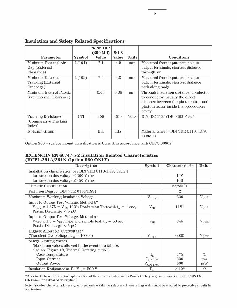
IEC/EN/DIN EN 60747-5-2 Insulation Related Characteristics(HCPL-261A/261N Option 060 ONLY)
Description Symbol Characteristic Units
Installation classification per DIN VDE 0110/1.89, Table 1for rated mains voltage ≤ 300 V rms I-IVfor rated mains voltage ≤ 450 V rms I-III
Climatic Classification 55/85/21Pollution Degree (DIN VDE 0110/1.89) 2Maximum Working Insulation Voltage VIORM 630 V peak
Input to Output Test Voltage, Method b*VIORM x 1.875 = VPR, 100% Production Test with tm = 1 sec, VPR 1181 V peak
Partial Discharge < 5 pCInput to Output Test Voltage, Method a*
VIORM x 1.5 = VPR, Type and sample test, tm = 60 sec, VPR 945 V peak
Partial Discharge < 5 pCHighest Allowable Overvoltage*(Transient Overvoltage, tini = 10 sec) VIOTM 6000 V peak
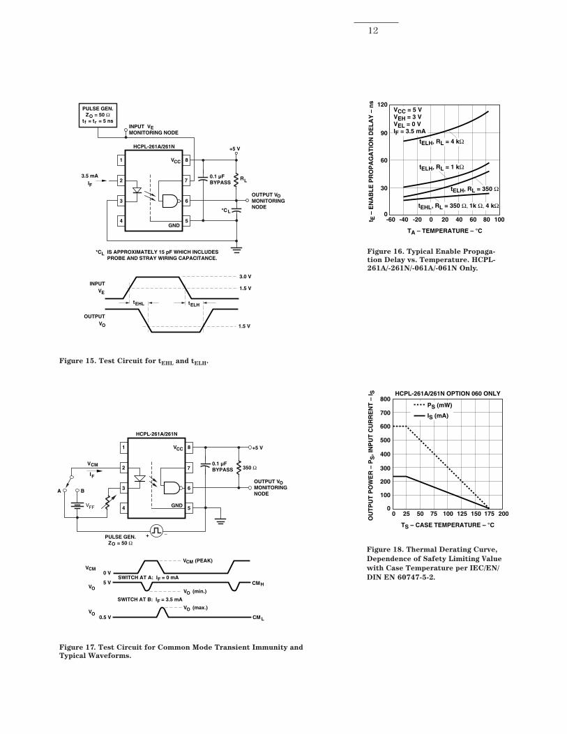
Safety Limiting Values(Maximum values allowed in the event of a failure,also see Figure 18, Thermal Derating curve.)
Case Temperature TS 175 °CInput Current IS,INPUT 230 mAOutput Power PS,OUTPUT 600 mW
Insulation Resistance at TS, VIO = 500 V RS ≥ 109 Ω
*Refer to the front of the optocoupler section of the current catalog, under Product Safety Regulations section IEC/EN/DIN EN60747-5-2 for a detailed description.
Note: Isolation characteristics are guaranteed only within the safety maximum ratings which must be ensured by protective circuits inapplication.
Insulation and Safety Related Specifications
8-Pin DIP
(300 Mil) SO-8
Parameter Symbol Value Value Units Conditions
Minimum External Air L(101) 7.1 4.9 mm Measured from input terminals toGap (External output terminals, shortest distanceClearance) through air.Minimum External L(102) 7.4 4.8 mm Measured from input terminals toTracking (External output terminals, shortest distanceCreepage) path along body.Minimum Internal Plastic 0.08 0.08 mm Through insulation distance, conductorGap (Internal Clearance) to conductor, usually the direct
distance between the photoemitter andphotodetector inside the optocouplercavity.
Tracking Resistance CTI 200 200 Volts DIN IEC 112/ VDE 0303 Part 1(Comparative TrackingIndex)Isolation Group IIIa IIIa Material Group (DIN VDE 0110, 1/89,
Table 1)
Option 300 – surface mount classification is Class A in accordance with CECC 00802.
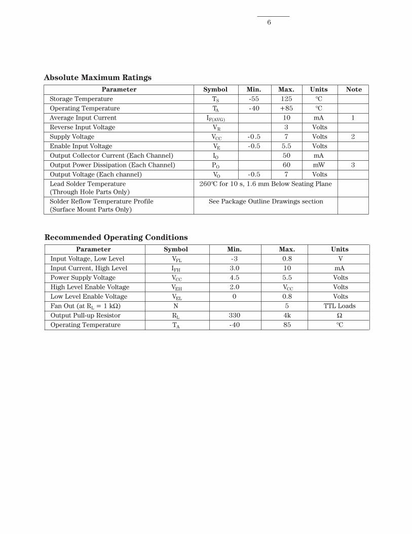
6
Absolute Maximum Ratings
Parameter Symbol Min. Max. Units Note
Storage Temperature TS -55 125 °COperating Temperature TA -40 +85 °CAverage Input Current IF(AVG) 10 mA 1Reverse Input Voltage VR 3 VoltsSupply Voltage VCC -0.5 7 Volts 2Enable Input Voltage VE -0.5 5.5 VoltsOutput Collector Current (Each Channel) IO 50 mAOutput Power Dissipation (Each Channel) PO 60 mW 3Output Voltage (Each channel) VO -0.5 7 VoltsLead Solder Temperature 260°C for 10 s, 1.6 mm Below Seating Plane(Through Hole Parts Only)Solder Reflow Temperature Profile See Package Outline Drawings section(Surface Mount Parts Only)
Recommended Operating Conditions
Parameter Symbol Min. Max. Units
Input Voltage, Low Level VFL -3 0.8 VInput Current, High Level IFH 3.0 10 mAPower Supply Voltage VCC 4.5 5.5 VoltsHigh Level Enable Voltage VEH 2.0 VCC VoltsLow Level Enable Voltage VEL 0 0.8 VoltsFan Out (at RL = 1 kΩ) N 5 TTL LoadsOutput Pull-up Resistor RL 330 4k ΩOperating Temperature TA -40 85 °C

7
Electrical SpecificationsOver recommended operating temperature (TA = -40°C to +85°C) unless otherwise specified.
Parameter Symbol Min. Typ.* Max. Units Test Conditions Fig. Note
High Level Output IOH 3.1 100 µA VCC = 5.5 V, VO = 5.5 V, 4 18Current VF = 0.8 V, VE = 2.0 VLow Level Output VOL 0.4 0.6 V VCC = 5.5 V, IOL = 13 mA 5, 8 4, 18Voltage (sinking), IF = 3.0 mA,
VE = 2.0 VHigh Level Supply ICCH 7 10 mA VE = 0.5 V** VCC = 5.5 V 4
9 15 Dual ChannelProducts***
Low Level Supply ICCL 8 13 mA VE = 0.5 V** VCC = 5.5 V12 21 Dual Channel
Products***High Level Enable IEH -0.6 -1.6 mA VCC = 5.5 V, VE = 2.0 VCurrent**Low Level Enable IEL -0.9 -1.6 mA VCC = 5.5 V, VE = 0.5 VCurrent**Input Forward VF 1.0 1.3 1.6 V IF = 4 mA 6 4VoltageTemperature Co- ∆VF/∆TA -1.25 mV/°C IF = 4 mA 4efficient of ForwardVoltageInput Reverse BVR 3 5 V IR = 100 µA 4Breakdown VoltageInput Capacitance CIN 60 pF f = 1 MHz, VF = 0 V
*All typical values at TA = 25°C, VCC = 5 V**Single Channel Products only (HCPL-261A/261N/061A/061N)***Dual Channel Products only (HCPL-263A/263N/063A/063N)
Current
Current
IF = 0 mA
IF = 3.0 mA
8
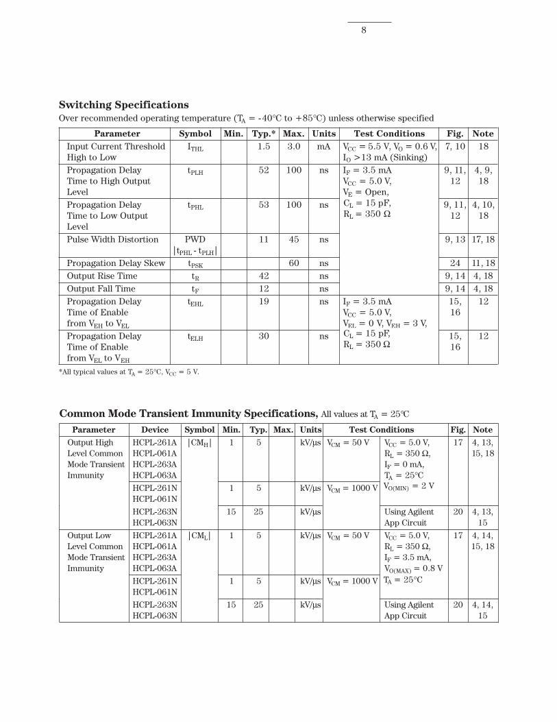
Common Mode Transient Immunity Specifications, All values at TA = 25°C
Parameter Device Symbol Min. Typ. Max. Units Test Conditions Fig. Note
Output High HCPL-261A |CMH| 1 5 kV/µs VCM = 50 V VCC = 5.0 V, 17 4, 13,Level Common HCPL-061A RL = 350 Ω, 15, 18Mode Transient HCPL-263A IF = 0 mA,Immunity HCPL-063A TA = 25°C
HCPL-261N 1 5 kV/µs VCM = 1000 VHCPL-061NHCPL-263N 15 25 kV/µs Using Agilent 20 4, 13,HCPL-063N App Circuit 15
Output Low HCPL-261A |CML| 1 5 kV/µs VCM = 50 V VCC = 5.0 V, 17 4, 14,Level Common HCPL-061A RL = 350 Ω, 15, 18Mode Transient HCPL-263A IF = 3.5 mA,Immunity HCPL-063A VO(MAX) = 0.8 V
HCPL-261N 1 5 kV/µs VCM = 1000 VHCPL-061NHCPL-263N 15 25 kV/µs Using Agilent 20 4, 14,HCPL-063N App Circuit 15
Switching SpecificationsOver recommended operating temperature (TA = -40°C to +85°C) unless otherwise specified
Parameter Symbol Min. Typ.* Max. Units Test Conditions Fig. Note
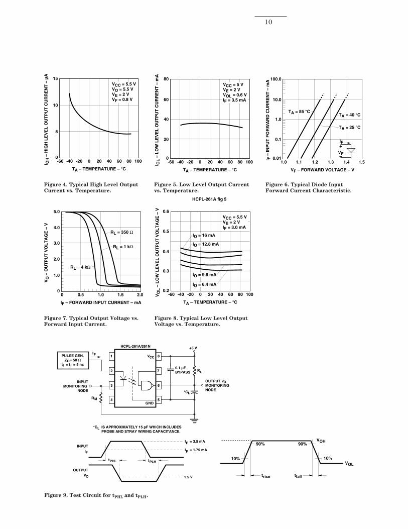
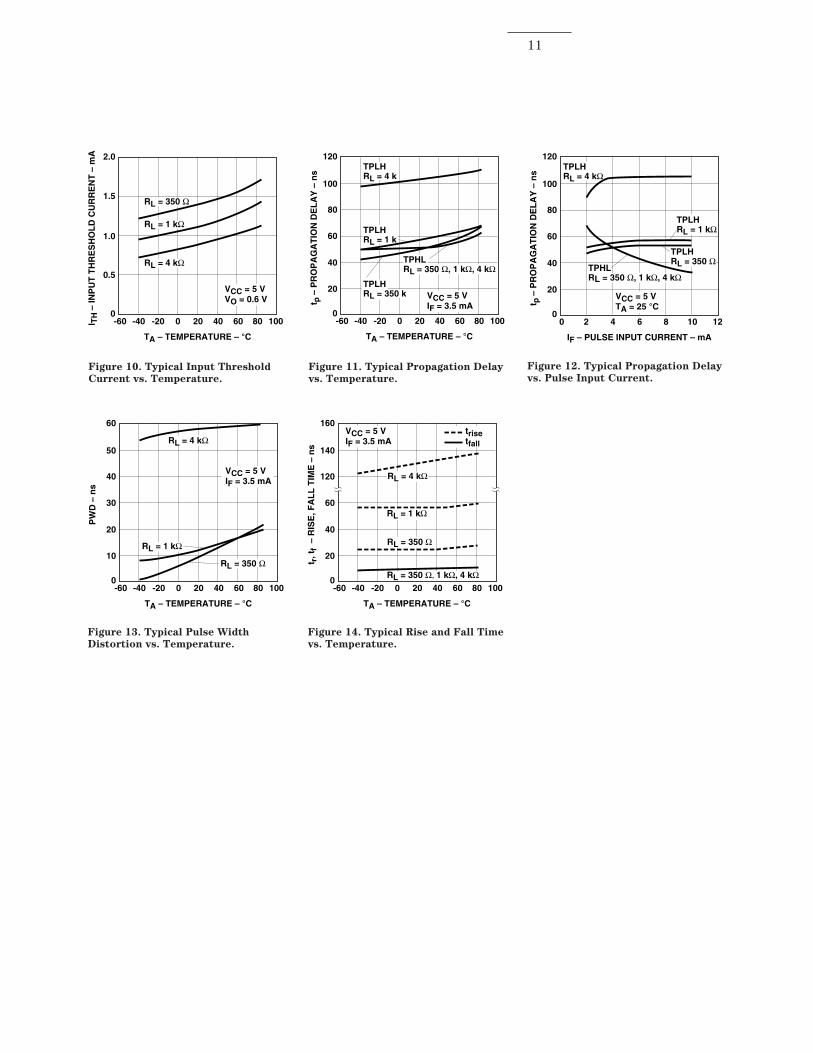
Input Current Threshold ITHL 1.5 3.0 mA VCC = 5.5 V, VO = 0.6 V, 7, 10 18High to Low IO >13 mA (Sinking)Propagation Delay tPLH 52 100 ns IF = 3.5 mA 9, 11, 4, 9,Time to High Output VCC = 5.0 V, 12 18Level VE = Open,Propagation Delay tPHL 53 100 ns 9, 11, 4, 10,Time to Low Output 12 18LevelPulse Width Distortion PWD 11 45 ns 9, 13 17, 18
|tPHL - tPLH|Propagation Delay Skew tPSK 60 ns 24 11, 18Output Rise Time tR 42 ns 9, 14 4, 18Output Fall Time tF 12 ns 9, 14 4, 18Propagation Delay tEHL 19 ns IF = 3.5 mA 15, 12Time of Enable VCC = 5.0 V, 16from VEH to VEL VEL = 0 V, VEH = 3 V,Propagation Delay tELH 30 ns 15, 12Time of Enable 16from VEL to VEH
*All typical values at TA = 25°C, VCC = 5 V.
CL = 15 pF,RL = 350 Ω
CL = 15 pF,RL = 350 Ω
VO(MIN) = 2 V
TA = 25°C
9
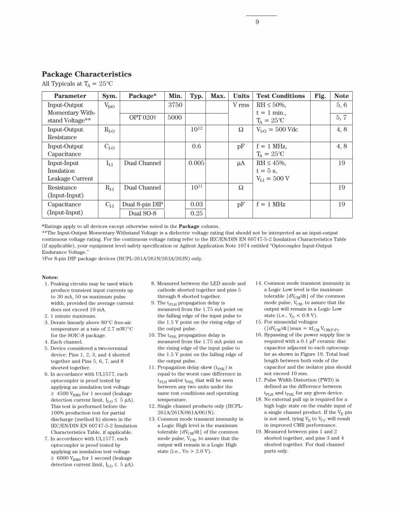
Package CharacteristicsAll Typicals at TA = 25°C
Parameter Sym. Package* Min. Typ. Max. Units Test Conditions Fig. Note
Input-Output VISO 3750 V rms RH ≤ 50%, 5, 6Momentary With- t = 1 min.,stand Voltage** TA = 25°CInput-Output RI-O 1012 Ω VI-O = 500 Vdc 4, 8ResistanceInput-Output CI-O 0.6 pF f = 1 MHz, 4, 8Capacitance TA = 25°CInput-Input II-I Dual Channel 0.005 µA RH ≤ 45%, 19Insulation t = 5 s,Leakage Current VI-I = 500 VResistance RI-I Dual Channel 1011 Ω 19(Input-Input)Capacitance CI-I Dual 8-pin DIP 0.03 pF f = 1 MHz 19
Dual SO-8 0.25
*Ratings apply to all devices except otherwise noted in the Package column.**The Input-Output Momentary Withstand Voltage is a dielectric voltage rating that should not be interpreted as an input-outputcontinuous voltage rating. For the continuous voltage rating refer to the IEC/EN/DIN EN 60747-5-2 Insulation Characteristics Table(if applicable), your equipment level safety specification or Agilent Application Note 1074 entitled “Optocoupler Input-OutputEndurance Voltage.”†For 8-pin DIP package devices (HCPL-261A/261N/263A/263N) only.
(Input-Input)
OPT 020† 5000 5, 7
Notes:
1. Peaking circuits may be used whichproduce transient input currents upto 30 mA, 50 ns maximum pulsewidth, provided the average currentdoes not exceed 10 mA.
2. 1 minute maximum.3. Derate linearly above 80°C free-air
temperature at a rate of 2.7 mW/°Cfor the SOIC-8 package.
4. Each channel.5. Device considered a two-terminal
device: Pins 1, 2, 3, and 4 shortedtogether and Pins 5, 6, 7, and 8shorted together.
6. In accordance with UL1577, eachoptocoupler is proof tested byapplying an insulation test voltage≥ 4500 VRMS for 1 second (leakagedetection current limit, II-O ≤ 5 µA).This test is performed before the100% production test for partialdischarge (method b) shown in theIEC/EN/DIN EN 60747-5-2 InsulationCharacteristics Table, if applicable.
7. In accordance with UL1577, eachoptocoupler is proof tested byapplying an insulation test voltage≥ 6000 VRMS for 1 second (leakagedetection current limit, II-O ≤ 5 µA).
8. Measured between the LED anode andcathode shorted together and pins 5through 8 shorted together.
9. The tPLH propagation delay ismeasured from the 1.75 mA point onthe falling edge of the input pulse tothe 1.5 V point on the rising edge ofthe output pulse.
10. The tPHL propagation delay ismeasured from the 1.75 mA point onthe rising edge of the input pulse tothe 1.5 V point on the falling edge ofthe output pulse.
11. Propagation delay skew (tPSK) isequal to the worst case difference intPLH and/or tPHL that will be seenbetween any two units under thesame test conditions and operatingtemperature.
12. Single channel products only (HCPL-261A/261N/061A/061N).
13. Common mode transient immunity ina Logic High level is the maximumtolerable |dVCM/dt| of the commonmode pulse, VCM, to assure that theoutput will remain in a Logic Highstate (i.e., Vo > 2.0 V).
14. Common mode transient immunity ina Logic Low level is the maximumtolerable |dVCM/dt| of the commonmode pulse, VCM, to assure that theoutput will remain in a Logic Lowstate (i.e., VO < 0.8 V).
15. For sinusoidal voltages(|dVCM/dt|)max = πfCM VCM(P-P).
16. Bypassing of the power supply line isrequired with a 0.1 µF ceramic disccapacitor adjacent to each optocoup-ler as shown in Figure 19. Total leadlength between both ends of thecapacitor and the isolator pins shouldnot exceed 10 mm.
17. Pulse Width Distortion (PWD) isdefined as the difference betweentPLH and tPHL for any given device.
18. No external pull up is required for ahigh logic state on the enable input ofa single channel product. If the VE pinis not used, tying VE to VCC will resultin improved CMR performance.
19. Measured between pins 1 and 2shorted together, and pins 3 and 4shorted together. For dual channelparts only.
10
OUTPUT V MONITORING NODE
O
1.5 V
tPHL tPLH
IF
INPUT
OVOUTPUT
I = 3.5 mA F
I = 1.75 mAF
+5 V
7
5
6
8
2
3
4
1PULSE GEN.Z = 50 Ω
t = t = 5 nsO
f
IF
LR
RM
CCV
0.1 µFBYPASS
*CL
*C IS APPROXIMATELY 15 pF WHICH INCLUDES PROBE AND STRAY WIRING CAPACITANCE.
L
GND
INPUTMONITORING
NODE
r
HCPL-261A/261N
VO
L –
LO
W L
EV
EL
OU
TP
UT
VO
LT
AG
E –
V
-600.2
TA – TEMPERATURE – °C
100
0.5
0.6
-20
0.3
20 60-40 0 40 80
0.4
VCC = 5.5 VVE = 2 VIF = 3.0 mA
IO = 16 mA
IO = 12.8 mA
IO = 9.6 mA
IO = 6.4 mA
I OL
– L
OW
LE
VE
L O
UT
PU
T C
UR
RE
NT
– m
A-60
0
TA – TEMPERATURE – °C
100
60
HCPL-261A fig 5
80
-20
20
20
VCC = 5 VVE = 2 VVOL = 0.6 VIF = 3.5 mA
60-40 0 40 80
40
I OH
– H
IGH
LE
VE
L O
UT
PU
T C
UR
RE
NT
– µ
A
-600
TA – TEMPERATURE – °C
100
10
15
-20
5
20
VCC = 5.5 VVO = 5.5 VVE = 2 VVF = 0.8 V
60-40 0 40 80
Figure 9. Test Circuit for tPHL and tPLH.
90% 90%
10% 10%
trise tfall
VOH
VOL
VO
– O
UT
PU
T V
OL
TA
GE
– V
00
IF – FORWARD INPUT CURRENT – mA
2.0
4.0
5.0
1.0
2.0
0.5 1.5
3.0
1.0
RL = 4 kΩ
RL = 350 Ω
RL = 1 kΩ
Figure 4. Typical High Level OutputCurrent vs. Temperature.
I F –
INP
UT
FO
RW
AR
D C
UR
RE
NT
– m
A
1.00.01
VF – FORWARD VOLTAGE – V
1.5
10.0
100.0
1.2
0.1
1.41.1 1.3
1.0
TA = 85 °CTA = 40 °C
TA = 25 °C
IF+
–VF
Figure 6. Typical Diode InputForward Current Characteristic.
Figure 5. Low Level Output Currentvs. Temperature.
Figure 7. Typical Output Voltage vs.Forward Input Current.
Figure 8. Typical Low Level OutputVoltage vs. Temperature.
11
t r, t
f –
RIS
E, F
AL
L T
IME
– n
s
-600
TA – TEMPERATURE – °C
100
140
160
-20
40
20 60-40 0 40 80
60
120
20
VCC = 5 VIF = 3.5 mA
RL = 4 kΩ
RL = 1 kΩ
RL = 350 Ω, 1 kΩ, 4 kΩ
trisetfall
RL = 350 Ω
PW
D –
ns
-600
TA – TEMPERATURE – °C
100
50
60
-20
20
20 60-40 0 40 80
30
40
10RL = 1 kΩ
RL = 350 Ω
VCC = 5 VIF = 3.5 mA
RL = 4 kΩ
t p –
PR
OP
AG
AT
ION
DE
LA
Y –
ns
00
IF – PULSE INPUT CURRENT – mA
12
100
120
2
40
6 84 10
60
80
20
TPLHRL = 4 kΩ
VCC = 5 VTA = 25 °C
TPLHRL = 1 kΩ
TPHLRL = 350 Ω, 1 kΩ, 4 kΩ
TPLHRL = 350 Ω
t p –
PR
OP
AG
AT
ION
DE
LA
Y –
ns
-600
TA – TEMPERATURE – °C
100
100
120
-20
40
20 60-40 0 40 80
60
80
20
TPLHRL = 4 k
TPLHRL = 1 k
TPLHRL = 350 k
TPHLRL = 350 Ω, 1 kΩ, 4 kΩ
VCC = 5 VIF = 3.5 mA
I TH
– IN
PU
T T
HR
ES
HO
LD
CU
RR
EN
T –
mA
-600
TA – TEMPERATURE – °C
100
1.5
2.0
-20
0.5
20 60-40 0 40 80
1.0
VCC = 5 VVO = 0.6 V
RL = 350 Ω
RL = 1 kΩ
RL = 4 kΩ
Figure 10. Typical Input ThresholdCurrent vs. Temperature.
Figure 13. Typical Pulse WidthDistortion vs. Temperature.
Figure 11. Typical Propagation Delayvs. Temperature.
Figure 12. Typical Propagation Delayvs. Pulse Input Current.
Figure 14. Typical Rise and Fall Timevs. Temperature.
12
VO0.5 V
OV (min.)
5 V
0 VSWITCH AT A: I = 0 mAF
SWITCH AT B: I = 3.5 mAF
CMV
HCM
CM L
OV (max.)
CMV (PEAK)
VO
+5 V
7
5
6
8
2
3
4
1 CCV
0.1 µFBYPASS
GND
OUTPUT V MONITORING NODE
O
PULSE GEN.Z = 50 ΩO
+_
350 ΩIF
BA
VFF
CMV
HCPL-261A/261N
t E –
EN
AB
LE
PR
OP
AG
AT
ION
DE
LA
Y –
ns
-600
TA – TEMPERATURE – °C
100
90
120
-20
30
20 60-40 0 40 80
60
VCC = 5 VVEH = 3 VVEL = 0 VIF = 3.5 mA
tELH, RL = 4 kΩ
tELH, RL = 1 kΩ
tEHL, RL = 350 Ω, 1k Ω, 4 kΩ
tELH, RL = 350 ΩOUTPUT V MONITORING NODE
O
1.5 V
tEHL tELH
VE
INPUT
OVOUTPUT
3.0 V
1.5 V
+5 V
7
5
6
8
2
3
4
1
PULSE GEN.Z = 50 Ω
t = t = 5 nsO
f
IFLR
CCV
0.1 µFBYPASS
*CL
*C IS APPROXIMATELY 15 pF WHICH INCLUDES PROBE AND STRAY WIRING CAPACITANCE.
L
GND
r
3.5 mA
INPUT VEMONITORING NODE
HCPL-261A/261N
Figure 15. Test Circuit for tEHL and tELH.
Figure 17. Test Circuit for Common Mode Transient Immunity andTypical Waveforms.
Figure 16. Typical Enable Propaga-tion Delay vs. Temperature. HCPL-261A/-261N/-061A/-061N Only.
Figure 18. Thermal Derating Curve,
Dependence of Safety Limiting Value
with Case Temperature per IEC/EN/
DIN EN 60747-5-2.
OU
TP
UT
PO
WE
R –
PS
, IN
PU
T C
UR
RE
NT
– I S
00
TS – CASE TEMPERATURE – °C
20050
400
12525 75 100 150
600
800
200
100
300
500
700PS (mW)
IS (mA)
HCPL-261A/261N OPTION 060 ONLY
175
13
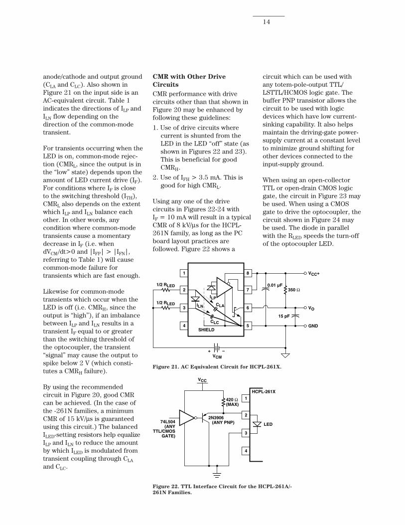
Figure 20. Recommended Drive Circuit for HCPL-261A/-261N Families for High-CMR (Similar for HCPL-263A/-263N).
Application InformationCommon-Mode Rejection for
HCPL-261A/HCPL-261N
Families:
Figure 20 shows the recom-mended drive circuit for theHCPL-261N/-261A for optimalcommon-mode rejectionperformance. Two main points tonote are:
1. The enable pin is tied to VCCrather than floating (thisapplies to single-channel partsonly).
2. Two LED-current settingresistors are used instead ofone. This is to balance ILEDvariation during common-mode transients.
If the enable pin is left floating, itis possible for common-modetransients to couple to the enablepin, resulting in common-modefailure. This failure mechanismonly occurs when the LED is onand the output is in the LowState. It is identified as occurringwhen the transient output voltagerises above 0.8 V. Therefore, theenable pin should be connectedto either VCC or logic-level highfor best common-modeperformance with the output low(CMRL). This failure mechanismis only present in single-channelparts (HCPL-261N, -261A,-061N, -061A) which have theenable function.
Also, common-mode transientscan capacitively couple from theLED anode (or cathode) to theoutput-side ground causingcurrent to be shunted away fromthe LED (which can be bad if theLED is on) or conversely causecurrent to be injected into theLED (bad if the LED is meant tobe off). Figure 21 shows theparasitic capacitances whichexists between LED
*Higher CMR May Be Obtainable by Connecting Pins 1, 4 to Input Ground (Gnd1).
ENABLE(IF USED)
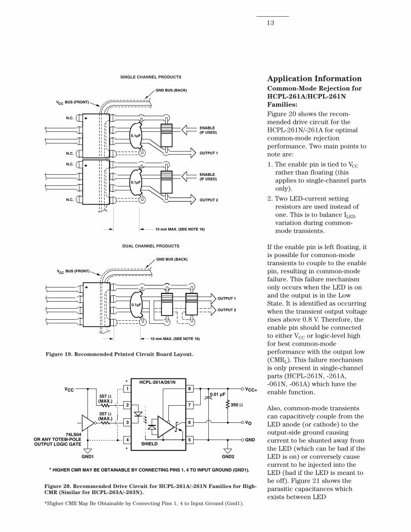
GND BUS (BACK)
V BUS (FRONT)CC
N.C.
N.C.
N.C.
N.C.
OUTPUT 1
OUTPUT 2
ENABLE(IF USED)
0.1µF
0.1µF
10 mm MAX. (SEE NOTE 16)
SINGLE CHANNEL PRODUCTS
0.01 µF
350 Ω
74LS04OR ANY TOTEM-POLEOUTPUT LOGIC GATE
VO
VCC+8
7
6
1
3
SHIELD5
2
4
HCPL-261A/261N
GND
GND2
357 Ω(MAX.)
VCC
357 Ω(MAX.)
*
*
* HIGHER CMR MAY BE OBTAINABLE BY CONNECTING PINS 1, 4 TO INPUT GROUND (GND1).
GND1
Figure 19. Recommended Printed Circuit Board Layout.
GND BUS (BACK)
V BUS (FRONT)CC
OUTPUT 1
OUTPUT 20.1µF
10 mm MAX. (SEE NOTE 16)
DUAL CHANNEL PRODUCTS
14
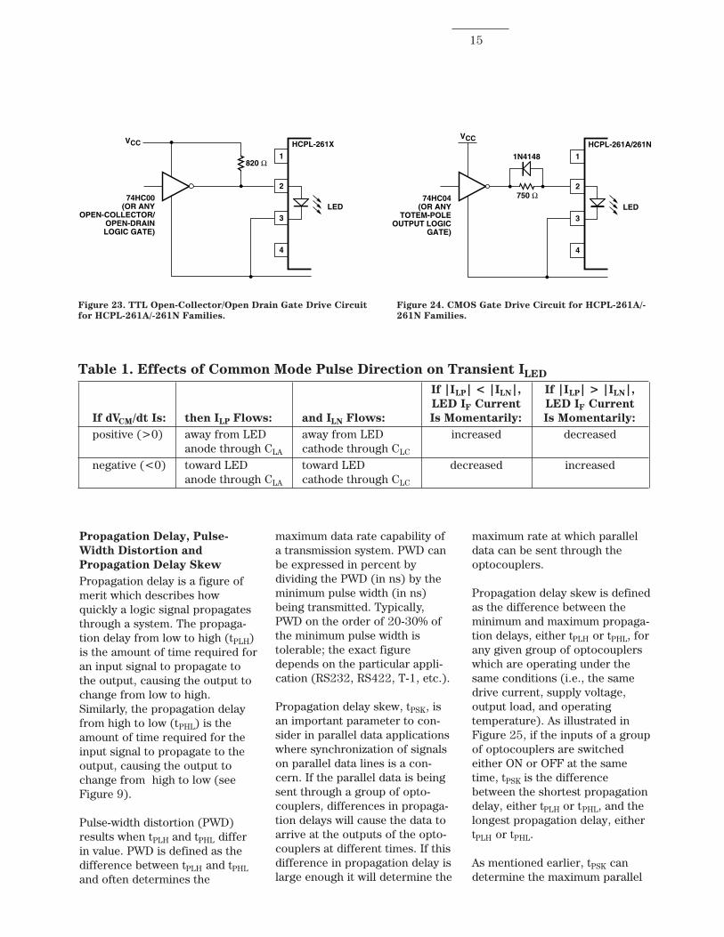
Figure 22. TTL Interface Circuit for the HCPL-261A/-261N Families.
420 Ω(MAX)
1
3
2
4
2N3906 (ANY PNP)
VCC
74L504(ANY
TTL/CMOSGATE)
HCPL-261X
LED
anode/cathode and output ground(CLA and CLC). Also shown inFigure 21 on the input side is anAC-equivalent circuit. Table 1indicates the directions of ILP andILN flow depending on thedirection of the common-modetransient.
For transients occurring when theLED is on, common-mode rejec-tion (CMRL, since the output is inthe “low” state) depends upon theamount of LED current drive (IF).For conditions where IF is closeto the switching threshold (ITH),CMRL also depends on the extentwhich ILP and ILN balance eachother. In other words, anycondition where common-modetransients cause a momentarydecrease in IF (i.e. whendVCM/dt>0 and |IFP| > |IFN|,referring to Table 1) will causecommon-mode failure fortransients which are fast enough.
Likewise for common-modetransients which occur when theLED is off (i.e. CMRH, since theoutput is “high”), if an imbalancebetween ILP and ILN results in atransient IF equal to or greaterthan the switching threshold ofthe optocoupler, the transient“signal” may cause the output tospike below 2 V (which consti-tutes a CMRH failure).
By using the recommendedcircuit in Figure 20, good CMRcan be achieved. (In the case ofthe -261N families, a minimumCMR of 15 kV/µs is guaranteedusing this circuit.) The balancedILED-setting resistors help equalizeILP and ILN to reduce the amountby which ILED is modulated fromtransient coupling through CLAand CLC.
CMR with Other Drive
Circuits
CMR performance with drivecircuits other than that shown inFigure 20 may be enhanced byfollowing these guidelines:
1. Use of drive circuits wherecurrent is shunted from theLED in the LED “off” state (asshown in Figures 22 and 23).This is beneficial for goodCMRH.
2. Use of IFH > 3.5 mA. This isgood for high CMRL.
Using any one of the drivecircuits in Figures 22-24 withIF = 10 mA will result in a typicalCMR of 8 kV/µs for the HCPL-261N family, as long as the PCboard layout practices arefollowed. Figure 22 shows a
circuit which can be used withany totem-pole-output TTL/LSTTL/HCMOS logic gate. Thebuffer PNP transistor allows thecircuit to be used with logicdevices which have low current-sinking capability. It also helpsmaintain the driving-gate power-supply current at a constant levelto minimize ground shifting forother devices connected to theinput-supply ground.
When using an open-collectorTTL or open-drain CMOS logicgate, the circuit in Figure 23 maybe used. When using a CMOSgate to drive the optocoupler, thecircuit shown in Figure 24 maybe used. The diode in parallelwith the RLED speeds the turn-offof the optocoupler LED.
Figure 21. AC Equivalent Circuit for HCPL-261X.
350 Ω1/2 RLED
VCC+
15 pF
+VCM
8
7
6
1
3
SHIELD5
2
4
CLA VO
GND
0.01 µF
1/2 RLED
CLC
ILN
ILP
–
15
Figure 24. CMOS Gate Drive Circuit for HCPL-261A/-261N Families.
Table 1. Effects of Common Mode Pulse Direction on Transient ILED
If |ILP| < |ILN|, If |ILP| > |ILN|,
LED IF Current LED IF Current
If dVCM/dt Is: then ILP Flows: and ILN Flows: Is Momentarily: Is Momentarily:
positive (>0) away from LED away from LED increased decreasedanode through CLA cathode through CLC
negative (<0) toward LED toward LED decreased increasedanode through CLA cathode through CLC
Figure 23. TTL Open-Collector/Open Drain Gate Drive Circuitfor HCPL-261A/-261N Families.
820 Ω1
3
2
4
VCC
74HC00(OR ANY
OPEN-COLLECTOR/OPEN-DRAINLOGIC GATE)
HCPL-261X
LED750 Ω
1
3
2
4
VCC
74HC04(OR ANY
TOTEM-POLEOUTPUT LOGIC
GATE)
HCPL-261A/261N
1N4148
LED
Propagation Delay, Pulse-
Width Distortion and
Propagation Delay Skew
Propagation delay is a figure ofmerit which describes howquickly a logic signal propagatesthrough a system. The propaga-tion delay from low to high (tPLH)is the amount of time required foran input signal to propagate tothe output, causing the output tochange from low to high.Similarly, the propagation delayfrom high to low (tPHL) is theamount of time required for theinput signal to propagate to theoutput, causing the output tochange from high to low (seeFigure 9).
Pulse-width distortion (PWD)results when tPLH and tPHL differin value. PWD is defined as thedifference between tPLH and tPHLand often determines the
maximum data rate capability ofa transmission system. PWD canbe expressed in percent bydividing the PWD (in ns) by theminimum pulse width (in ns)being transmitted. Typically,PWD on the order of 20-30% ofthe minimum pulse width istolerable; the exact figuredepends on the particular appli-cation (RS232, RS422, T-1, etc.).
Propagation delay skew, tPSK, isan important parameter to con-sider in parallel data applicationswhere synchronization of signalson parallel data lines is a con-cern. If the parallel data is beingsent through a group of opto-couplers, differences in propaga-tion delays will cause the data toarrive at the outputs of the opto-couplers at different times. If thisdifference in propagation delay islarge enough it will determine the
maximum rate at which paralleldata can be sent through theoptocouplers.
Propagation delay skew is definedas the difference between theminimum and maximum propaga-tion delays, either tPLH or tPHL, forany given group of optocouplerswhich are operating under thesame conditions (i.e., the samedrive current, supply voltage,output load, and operatingtemperature). As illustrated inFigure 25, if the inputs of a groupof optocouplers are switchedeither ON or OFF at the sametime, tPSK is the differencebetween the shortest propagationdelay, either tPLH or tPHL, and thelongest propagation delay, eithertPLH or tPHL.
As mentioned earlier, tPSK candetermine the maximum parallel
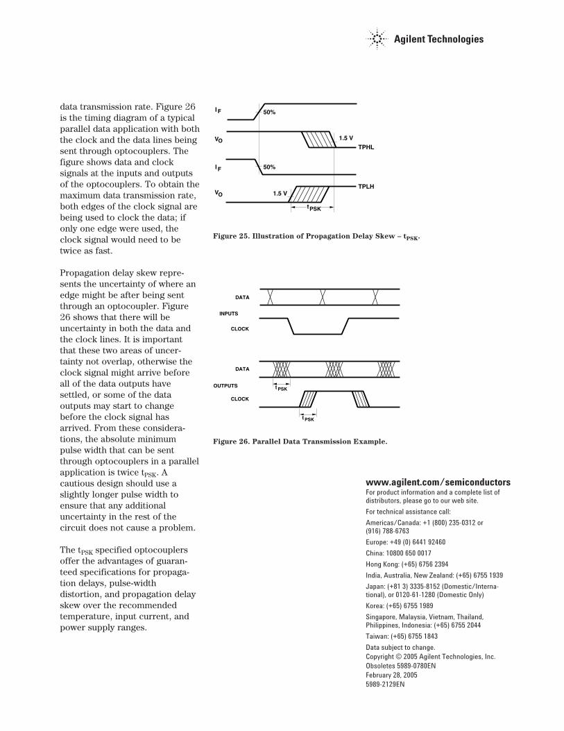
Figure 25. Illustration of Propagation Delay Skew – tPSK.
50%
1.5 V
I F
VO
50%I F
VO
tPSK
1.5 V
TPHL
TPLH
Figure 26. Parallel Data Transmission Example.
DATA
t PSK
INPUTS
CLOCK
DATA
OUTPUTS
CLOCK
t PSK
data transmission rate. Figure 26is the timing diagram of a typicalparallel data application with boththe clock and the data lines beingsent through optocouplers. Thefigure shows data and clocksignals at the inputs and outputsof the optocouplers. To obtain themaximum data transmission rate,both edges of the clock signal arebeing used to clock the data; ifonly one edge were used, theclock signal would need to betwice as fast.
Propagation delay skew repre-sents the uncertainty of where anedge might be after being sentthrough an optocoupler. Figure26 shows that there will beuncertainty in both the data andthe clock lines. It is importantthat these two areas of uncer-tainty not overlap, otherwise theclock signal might arrive beforeall of the data outputs havesettled, or some of the dataoutputs may start to changebefore the clock signal hasarrived. From these considera-tions, the absolute minimumpulse width that can be sentthrough optocouplers in a parallelapplication is twice tPSK. Acautious design should use aslightly longer pulse width toensure that any additionaluncertainty in the rest of thecircuit does not cause a problem.
The tPSK specified optocouplersoffer the advantages of guaran-teed specifications for propaga-tion delays, pulse-widthdistortion, and propagation delayskew over the recommendedtemperature, input current, andpower supply ranges.
www.agilent.com/semiconductorsFor product information and a complete list ofdistributors, please go to our web site.
For technical assistance call:
Americas/Canada: +1 (800) 235-0312 or(916) 788-6763
Europe: +49 (0) 6441 92460
China: 10800 650 0017
Hong Kong: (+65) 6756 2394
India, Australia, New Zealand: (+65) 6755 1939
Japan: (+81 3) 3335-8152 (Domestic/Interna-tional), or 0120-61-1280 (Domestic Only)
Korea: (+65) 6755 1989
Singapore, Malaysia, Vietnam, Thailand,Philippines, Indonesia: (+65) 6755 2044
Taiwan: (+65) 6755 1843
Data subject to change.Copyright © 2005 Agilent Technologies, Inc.Obsoletes 5989-0780ENFebruary 28, 20055989-2129EN