Embed Size (px)
Citation preview

FN2845Rev 13.00
August 11, 2015
HA-5020100MHz Current FeedbackVideo Amplifier With Disable
DATASHEET
The HA-5020 is a wide bandwidth, high slew rate amplifier optimized for video applications and gains between 1 and 10. Manufactured on Intersil’s Reduced Feature Complementary Bipolar DI process, this amplifier uses current mode feedback to maintain higher bandwidth at a given gain than conventional voltage feedback amplifiers. Since it is a closed loop device, the HA-5020 offers better gain accuracy and lower distortion than open loop buffers.
The HA-5020 features low differential gain and phase and will drive two double terminated 75 coax cables to video levels with low distortion. Adding a gain flatness performance of 0.1dB makes this amplifier ideal for demanding video applications. The bandwidth and slew rate of the HA-5020 are relatively independent of closed loop gain. The 100MHz unity gain bandwidth only decreases to 60MHz at a gain of 10. The HA-5020 used in place of a conventional op amp will yield a significant improvement in the speed power product. To further reduce power, HA-5020 has a disable function which significantly reduces supply current, while forcing the output to a true high impedance state. This allows the outputs of multiple amplifiers to be wire-OR’d into multiplexer configurations. The device also includes output short circuit protection and output offset voltage adjustment.For multi channel versions of the HA-5020 see the HA5022 dual with disable, HA5023 dual, HA5013 triple and HA5024 quad with disable op amp data sheets.
PinoutHA-5020
(PDIP, SOIC)TOP VIEW
Features
• Wide Unity Gain Bandwidth . . . . . . . . . . . . . . . . . 100MHz
• Slew Rate. . . . . . . . . . . . . . . . . . . . . . . . . . . . . . . 800V/µs
• Output Current . . . . . . . . . . . . . . . . . . . . . . . ±30mA (Min)
• Drives 3.5V into 75
• Differential Gain . . . . . . . . . . . . . . . . . . . . . . . . . . . 0.03%
• Differential Phase. . . . . . . . . . . . . . . . . . . . . . . . . . . .0.03°
• Low Input Voltage Noise . . . . . . . . . . . . . . . . . 4.5nV/Hz
• Low Supply Current . . . . . . . . . . . . . . . . . . . . 10mA (Max)
• Wide Supply Range . . . . . . . . . . . . . . . . . . . ±5V to ±15V
• Output Enable/Disable
• High Performance Replacement for EL2020
• Pb-Free (RoHS Compliant)
Applications
• Unity Gain Video/Wideband Buffer
• Video Gain Block
• Video Distribution Amp/Coax Cable Driver
• Flash A/D Driver
• Waveform Generator Output Driver
• Current to Voltage Converter; D/A Output Buffer
• Radar Systems
• Imaging Systems
BAL
IN-
IN+
V-
1
2
3
4
8
7
6
5
DISABLE
V+
OUT
BAL
+-
FN2845 Rev 13.00 Page 1 of 23August 11, 2015

HA-5020
Ordering Information
PART NUMBER
PART MARKING
TEMP. RANGE(°C)
PACKAGE(PB-free
PKG.DWG. #
HA3-5020-5Z (Note 2)(No longer available, recommended replacement: HA9P5020-5Z, HA9P5020-5ZX96)
HA3- 5020-5Z 0 to +75 8 Ld PDIP E8.3
HA9P5020-5Z (Note 2) 50205Z 0 to +75 8 Ld SOIC M8.15
HA9P5020-5ZX96 (Note 1) 50205Z 0 to +75 8 Ld SOIC (Tape and Reel) M8.15
NOTES:
1. Please refer to TB347 for details on reel specifications.
2. These Intersil Pb-free plastic packaged products employ special Pb-free material sets, molding compounds/die attach materials, and 100% matte tin plate plus anneal (e3 termination finish, which is RoHS compliant and compatible with both SnPb and Pb-free soldering operations). Intersil Pb-free products are MSL classified at Pb-free peak reflow temperatures that meet or exceed the Pb-free requirements of IPC/JEDEC J STD-020.
FN2845 Rev 13.00 Page 2 of 23August 11, 2015

HA-5020
Absolute Maximum Ratings (Note 3) Thermal Information
Voltage Between V+ and V- Terminals . . . . . . . . . . . . . . . . . . . 36VDC Input Voltage . . . . . . . . . . . . . . . . . . . . . . . . . . . . . . . ±VSUPPLYDifferential Input Voltage . . . . . . . . . . . . . . . . . . . . . . . . . . . . . . 10VOutput Current . . . . . . . . . . . . . . . . . . . . . . . Short Circuit Protected
Operating ConditionsTemperature Range. . . . . . . . . . . . . . . . . . . . . . . . . . . 0°C to +75°C
Thermal Resistance (Typical, Note 4) JA (°C/W) JC (°C/W)PDIP Package* . . . . . . . . . . . . . . . . . . 120 N/ASOIC Package . . . . . . . . . . . . . . . . . . . 165 N/A
Maximum Junction Temperature (Plastic Packages, Note 3) . . +150°CMaximum Storage Temperature Range . . . . . . . . -65°C to +150°C*Pb-free PDIPs can be used for through hole wave solder process-ing only. They are not intended for use in Reflow solder processingapplicationsPb-Free Reflow Profile. . . . . . . . . . . . . . . . . . . . . . . . .see link below
http://www.intersil.com/pbfree/Pb-FreeReflow.asp
CAUTION: Stresses above those listed in “Absolute Maximum Ratings” may cause permanent damage to the device. This is a stress only rating and operation of thedevice at these or any other conditions above those indicated in the operational sections of this specification is not implied.
NOTES:
3. Maximum power dissipation, including output load, must be designed to maintain junction temperature below +150°C for plastic packages.
4. JA is measured with the component mounted on a low effective thermal conductivity test board in free air. See Tech Brief TB379 for details.
Electrical Specifications VSUPPLY = 15V, RF = 1k AV = +1, RL = 400 CL 10pF,Unless Otherwise Specified
PARAMETER TEST CONDITIONSTEMP.
(°C) MIN TYP MAX UNITS
INPUT CHARACTERISTICS
Input Offset Voltage (Notes 6, 17) 25 - 2 8 mV
Full - - 10 mV
Average Input Offset Voltage Drift Full - 10 - µV/°C
VIO Common Mode Rejection Ratio (Note 17) VCM = ±10V 25 60 - - dB
Full 50 - - dB
VIO Power Supply Rejection Ratio (Note 17) ±4.5V VS ±18V 25 64 - - dB
Full 60 - - dB
Non-Inverting Input (+IN) Current (Note 17) 25 - 3 8 µA
Full - - 20 µA
+IN Common Mode Rejection VCM = ±10V 25 - - 0.1 µA/V
Full - - 0.5 µA/V
+IN Power Supply Rejection ±4.5V VS ±18V 25 - - 0.06 µA/V
Full - - 0.2 µA/V
Inverting Input (-IN) Current (Note 17) 25 - 12 20 µA
Full - 25 50 µA
-IN Common Mode Rejection VCM = ±10V 25 - - 0.4 µA/V
Full - - 0.5 µA/V
-IN Power Supply Rejection ±4.5V VS ±18V 25 - - 0.2 µA/V
Full - - 0.5 µA/V
TRANSFER CHARACTERISTICS
Transimpedance (Notes 12, 17) 25 3500 - - V/mA
Full 1000 - - V/mA
Open Loop DC Voltage Gain (Note 12) RL = 400,VOUT = ±10V
25 70 - - dB
Full 65 - - dB
Open Loop DC Voltage Gain RL = 100,VOUT = ±2.5V
25 60 - - dB
Full 55 - - dB
FN2845 Rev 13.00 Page 3 of 23August 11, 2015

HA-5020
OUTPUT CHARACTERISTICS
Output Voltage Swing (Note 17) RL = 150 25 to 85 12 12.7 - V
-40 to 0 11 11.8 - V
Output Current (Guaranteed by Output Voltage Test) 25 30 31.7 - mA
Full 27.5 - - mA
POWER SUPPLY CHARACTERISTICS
Quiescent Supply Current (Note 17) Full - 7.5 10 mA
Supply Current, Disabled (Note 17) DISABLE = 0V Full - 5 7.5 mA
Disable Pin Input Current DISABLE = 0V Full - 1.0 1.5 mA
Minimum Pin 8 Current to Disable (Note 7) Full 350 - - µA
Maximum Pin 8 Current to Enable (Note 8) Full - - 20 µA
AC CHARACTERISTICS (AV = +1)
Slew Rate (Note 9) 25 600 800 - V/µs
Full 500 700 - V/µs
Full Power Bandwidth (Note 10)(Guaranteed by Slew Rate Test)
25 9.6 12.7 - MHz
Full 8.0 11.1 - MHz
Rise Time (Note 11) 25 - 5 - ns
Fall Time (Note 11) 25 - 5 - ns
Propagation Delay (Notes 11, 17) 25 - 6 - ns
-3dB Bandwidth (Note 17) VOUT = 100mV 25 - 100 - MHz
Settling Time to 1% 10V Output Step 25 - 45 - ns
Settling Time to 0.25% 10V Output Step 25 - 100 - ns
AC CHARACTERISTICS (AV = +10, RF = 383)
Slew Rate (Notes 9, 12) 25 900 1100 - V/µs
Full 700 - - V/µs
Full Power Bandwidth (Note 10)(Guaranteed by Slew Rate Test)
25 14.3 17.5 - MHz
Full 11.1 - - MHz
Rise Time (Note 11) 25 - 8 - ns
Fall Time (Note 11) 25 - 8 - ns
Propagation Delay (Notes 11, 17) 25 - 9 - ns
-3dB Bandwidth VOUT = 100mV 25 - 60 - MHz
Settling Time to 1% 10V Output Step 25 - 55 - ns
Settling Time to 0.1% 10V Output Step 25 - 90 - ns
INTERSIL VALUE ADDED SPECIFICATIONS
Input Noise Voltage (Note 17) f = 1kHz 25 - 4.5 - nV/Hz
+Input Noise Current (Note 17) f = 1kHz 25 - 2.5 - pA/Hz
-Input Noise Current (Note 17) f = 1kHz 25 - 25 - pA/Hz
Input Common Mode Range Full 10 12 - V
-IBIAS Adjust Range (Note 6) Full 25 40 - µA
Overshoot (Note 17) 25 - 7 - %
Electrical Specifications VSUPPLY = 15V, RF = 1k AV = +1, RL = 400 CL 10pF,Unless Otherwise Specified (Continued)
PARAMETER TEST CONDITIONSTEMP.
(°C) MIN TYP MAX UNITS
FN2845 Rev 13.00 Page 4 of 23August 11, 2015

HA-5020
Output Current, Short Circuit (Note 17) VIN = 10V, VOUT = 0V Full 50 65 - mA
Output Current, Disabled (Note 17) DISABLE = 0V, VOUT = 10V
Full - - 1 µA
Output Disable Time (Notes 13, 17) 25 - 10 - µs
Output Enable Time (Notes 14, 17) 25 - 200 - ns
Supply Voltage Range 25 ±5 - ±15 V
Output Capacitance, Disabled (Note 15) DISABLE = 0V 25 - 6 - pF
VIDEO CHARACTERISTICS
Differential Gain (Notes 16, 17) RL = 150 25 - 0.03 - %
Differential Phase (Notes 16, 17) RL = 150 25 - 0.03 - °
Gain Flatness To 5MHz 25 - 0.1 - dB
Electrical Specifications V+ = +5V, V- = -5V, RF = 1k AV = +1, RL = 400 CL 10pF, Unless Otherwise Specified.Parameters are not tested. The limits are guaranteed based on lab characterizations, and reflectlot-to-lot variation.
PARAMETER TEST CONDITIONSTEMP.
(°C) MIN TYP MAX UNITS
INPUT CHARACTERISTICS
Input Offset Voltage (Notes 6, 17) 25 - 2 8 mV
Full - - 10 mV
Average Input Offset Voltage Drift Full - 10 - µV/°C
VIO Common Mode Rejection Ratio (Notes 17, 18) 25 50 - - dB
Full 35 - - dB
VIO Power Supply Rejection Ratio (Note 17) ±3.5V VS ±6.5V 25 55 - - dB
Full 50 - - dB
Non-Inverting Input (+IN) Current (Note 17) 25 - 3 8 µA
Full - - 20 µA
+IN Common Mode Rejection (Note 18) 25 - - 0.1 µA/V
Full - - 0.5 µA/V
+IN Power Supply Rejection ±3.5V VS ±6.5V 25 - - 0.06 µA/V
Full - - 0.2 µA/V
Inverting Input (-IN) Current (Note 17) 25 - 12 20 µA
Full - 25 50 µA
-IN Common Mode Rejection (Note 18) 25 - - 0.4 µA/V
Full - - 0.5 µA/V
-IN Power Supply Rejection ±3.5V VS ±6.5V 25 - - 0.2 µA/V
Full - - 0.5 µA/V
TRANSFER CHARACTERISTICS
Transimpedance (Notes 12, 17) 25 1000 - - V/mA
Full 850 - - V/mA
Open Loop DC Voltage Gain RL = 400, VOUT = ±2.5V
25 65 - - dB
Full 60 - - dB
Electrical Specifications VSUPPLY = 15V, RF = 1k AV = +1, RL = 400 CL 10pF,Unless Otherwise Specified (Continued)
PARAMETER TEST CONDITIONSTEMP.
(°C) MIN TYP MAX UNITS
FN2845 Rev 13.00 Page 5 of 23August 11, 2015

HA-5020
Open Loop DC Voltage Gain RL = 100, VOUT = 2.5V
25 50 - - dB
Full 45 - - dB
OUTPUT CHARACTERISTICS
Output Voltage Swing (Note 17) 25 to 85 ±2.5 ±3.0 - V
-40 to 0 ±2.5 ±3.0 - V
Output Current(Guaranteed by Output Voltage Test)
RL = 100 25 ±16.6 ±20 - mA
Full ±16.6 ±20 - mA
POWER SUPPLY CHARACTERISTICS
Quiescent Supply Current (Note 17) Full - 7.5 10 mA
Supply Current, Disabled (Note 17) DISABLE = 0V Full - 5 7.5 mA
Disable Pin Input Current DISABLE = 0V Full - 1.0 1.5 mA
Minimum Pin 8 Current to Disable (Note 19) Full 350 - - µA
Maximum Pin 8 Current to Enable (Note 8) Full - - 20 µA
AC CHARACTERISTICS (AV = +1)
Slew Rate (Note 20) 25 215 400 - V/µs
Full Power Bandwidth (Note 21) 25 22 28 - MHz
Rise Time (Note 11) 25 - 6 - ns
Fall Time (Note 11) 25 - 6 - ns
Propagation Delay (Note 11) 25 - 6 - ns
Overshoot 25 - 4.5 - %
-3dB Bandwidth (Note 17) VOUT = 100mV 25 - 125 - MHz
Settling Time to 1% 2V Output Step 25 - 50 - ns
Settling Time to 0.25% 2V Output Step 25 - 75 - ns
AC CHARACTERISTICS (AV = +2, RF = 681)
Slew Rate (Note 20) 25 - 475 - V/µs
Full Power Bandwidth (Note 21) 25 - 26 - MHz
Rise Time (Note 11) 25 - 6 - ns
Fall Time (Note 11) 25 - 6 - ns
Propagation Delay (Note 11) 25 - 6 - ns
Overshoot 25 - 12 - %
-3dB Bandwidth (Note 17) VOUT = 100mV 25 - 95 - MHz
Settling Time to 1% 2V Output Step 25 - 50 - ns
Settling Time to 0.25% 2V Output Step 25 - 100 - ns
AC CHARACTERISTICS (AV = +10, RF = 383)
Slew Rate (Note 20) 25 350 475 - V/µs
Full Power Bandwidth (Note 21) 25 28 38 - MHz
Rise Time (Note 11) 25 - 8 - ns
Fall Time (Note 11) 25 - 9 - ns
Propagation Delay (Note 11) 25 - 9 - ns
Overshoot 25 - 1.8 - %
Electrical Specifications V+ = +5V, V- = -5V, RF = 1k AV = +1, RL = 400 CL 10pF, Unless Otherwise Specified.Parameters are not tested. The limits are guaranteed based on lab characterizations, and reflectlot-to-lot variation. (Continued)
PARAMETER TEST CONDITIONSTEMP.
(°C) MIN TYP MAX UNITS
FN2845 Rev 13.00 Page 6 of 23August 11, 2015

HA-5020
-3dB Bandwidth (Note 17) VOUT = 100mV 25 - 65 - MHz
Settling Time to 1% 2V Output Step 25 - 75 - ns
Settling Time to 0.25% 2V Output Step 25 - 130 - ns
INTERSIL VALUE ADDED SPECIFICATIONS
Input Noise Voltage (Note 17) f = 1kHz 25 - 4.5 - nV/Hz
+Input Noise Current (Note 17) f = 1kHz 25 - 2.5 - pA/Hz
-Input Noise Current (Note 17) f = 1kHz 25 - 25 - pA/Hz
Input Common Mode Range Full ±2.5V - V
Output Current, Short Circuit VIN = ±2.5V, VOUT = 0V Full ±40 ±60 - mA
Output Current, Disabled (Note 17) DISABLE = 0V, VOUT = ±2.5V, VIN = 0V
Full - - 2 µA
Output Disable Time (Notes 17, 23) 25 - 40 - µs
Output Enable Time (Notes 17, 21) 25 - 40 - ns
Supply Voltage Range 25 ±5 - ±15 V
Output Capacitance, Disabled (Note 22) DISABLE = 0V 25 - 6 - pF
VIDEO CHARACTERISTICS
Differential Gain (Notes 16, 17) RL = 150 25 - 0.03 - %
Differential Phase (Notes 16, 17) RL = 150 25 - 0.03 - °
Gain Flatness To 5MHz 25 - 0.1 - dB
NOTES:
5. Suggested VOS Adjust Circuit: The inverting input current (-IBIAS) can be adjusted with an external 10k pot between pins 1 and 5, wiper connected to V+. Since -IBIAS flows through the feedback resistor (RF), the result is an adjustment in offset voltage. The amount of offset voltage adjustment is determined by the value of RF (VOS = -IBIAS*RF).
6. RL = 100, VIN = 10V. This is the minimum current which must be pulled out of the Disable pin in order to disable the output. The output is considered disabled when -10mV VOUT +10mV.
7. VIN = 0V. This is the maximum current that can be pulled out of the Disable pin with the HA-5020 remaining enabled. The HA-5020 is considered disabled when the supply current has decreased by at least 0.5mA.
8. VOUT switches from -10V to +10V, or from +10V to -10V. Specification is from the 25% to 75% points.
9.
10. RL = 100, VOUT = 1V. Measured from 10% to 90% points for rise/fall times; from 50% points of input and output for propagation delay. 11. This parameter is not tested. The limits are guaranteed based on lab characterization, and reflect lot-to-lot variation. 12. VIN = +10V, Disable = +15V to 0V. Measured from the 50% point of Disable to VOUT = 0V.13. VIN = +10V, Disable = 0V to +15V. Measured from the 50% point of Disable to VOUT = 10V.14. VIN = 0V, Force VOUT from 0V to ±10V, tR = tF = 50ns.15. Measured with a VM700A video tester using a NTC-7 composite VITS.16. See “Typical Performance Curves” on page 12 for more information.17. VCM = ±2.5V. At -40°C product is tested at VCM = ±2.25V because short test duration does not allow self heating.18. RL = 100. VIN = 2.5V. This is the minimum current which must be pulled out of the Disable pin in order to disable the output. The output is
considered disabled when -10mV VOUT +10mV.19. VOUT switches from -2V to +2V, or from +2V to -2V. Specification is from the 25% to 75% points.
20. FPBW = .
21. VIN = 0V, Force VOUT from 0V to 2.5V, tR = tF = 50ns.22. VIN = +2V, Disable = +5V to 0V. Measured from the 50% point of Disable to VOUT = 0V.23. VIN = +2V, Disable = 0V to +5V. Measured from the 50% point of Disable to VOUT = 2V.
Electrical Specifications V+ = +5V, V- = -5V, RF = 1k AV = +1, RL = 400 CL 10pF, Unless Otherwise Specified.Parameters are not tested. The limits are guaranteed based on lab characterizations, and reflectlot-to-lot variation. (Continued)
PARAMETER TEST CONDITIONSTEMP.
(°C) MIN TYP MAX UNITS
FPBWSlew Rate2VPEAK--------------------------- ; VPEAK = 10V.=
Slew Rate2VPEAK--------------------------- ; VPEAK = 2V
FN2845 Rev 13.00 Page 7 of 23August 11, 2015

HA-5020
Test Circuits and Waveforms
FIGURE 1. TEST CIRCUIT FOR TRANSIMPEDANCE MEASUREMENTS
FIGURE 2. SMALL SIGNAL PULSE RESPONSE CIRCUIT FIGURE 3. LARGE SIGNAL PULSE RESPONSE CIRCUIT
FIGURE 4. SMALL SIGNAL RESPONSE FIGURE 5. LARGE SIGNAL RESPONSE
+-
50
50
DUT
HP4195NETWORKANALYZER
VIN VOUT
RL
RF, 1k
10050
+-
DUT
VIN VOUT
RL
RF, 681
40050
+-
DUT
RI681
Vertical Scale: VIN = 100mV/Div., VOUT = 100mV/Div.Horizontal Scale: 20ns/Div.
VIN
VOUT
Vertical Scale: VIN = 1V/Div., VOUT = 1V/Div.Horizontal Scale: 50ns/Div.
VIN
VOUT
FN2845 Rev 13.00 Page 8 of 23August 11, 2015

HA-5020
Schematic Diagram
R2
800
R5
2.5
K
R6
15
KD
2
QP
2
R1
60
K
QN
1
R3
6K
QN
2
D1
QN
3
QN
4
R4
800
R7
15K
DIS
QN
7
R9
82
0
QP
4
QN
6Q
P3
R8
1.2
5K
QN
5
+IN
QP
7
R13
1KR1
22
80
QP
6
QN
8
QP
5
R10
820
QN
9Q
N11
QN
10
QP
10
QP
8Q
P9
R11
1K
R14
280
QN
14
R1
64
00
R2
22
80 Q
N16
R17
280
R1
82
80
QP
11
R15
400
R19
400
QP
14
QN
12
QP
12
-IN
QN
13
QP
13C
2
R23
40
0
R26
20
0
R24
14
0
R20
140
QP
15
C1
QN
17
R25
20
QN
18
R25
140
R2
11
40
R2
62
00
QP
16
R27
20
0
R33
2K
QP
18
QN
20
QP
17
R28
20
QN
15
R30
7
QN
19
O
QN
21
R32 5
R29
9.5
QP
19
QP
20
R3
1
5
V+
V-
QP
1
R33
80
0
1.4
pF
1.4
pF
FN2845 Rev 13.00 Page 9 of 23August 11, 2015

HA-5020
Application Information
Optimum Feedback Resistor
The plots of inverting and non-inverting frequency response illustrate the performance of the HA-5020 in various closed loop gain configurations. Although the bandwidth dependency on closed loop gain isn’t as severe as that of a voltage feedback amplifier, there can be an appreciable decrease in bandwidth at higher gains. This decrease may be minimized by taking advantage of the current feedback amplifier’s unique relationship between bandwidth and RF. All current feedback amplifiers require a feedback resistor, even for unity gain applications, and RF, in conjunction with the internal compensation capacitor, sets the dominant pole of the frequency response. Thus, the amplifier’s bandwidth is inversely proportional to RF. The HA-5020 design is optimized for a 1000 RF at a gain of +1. Decreasing RF in a unity gain application decreases stability, resulting in excessive peaking and overshoot. At higher gains the amplifier is more stable, so RF can be decreased in a trade-off of stability for bandwidth.
The table below lists recommended RF values for various gains, and the expected bandwidth.
PC Board Layout
The frequency response of this amplifier depends greatly on the amount of care taken in designing the PC board. The use of low inductance components such as chip resistors and chip capacitors is strongly recommended. If leaded components are used the leads must be kept short especially for the power supply decoupling components and those components connected to the inverting input.
Attention must be given to decoupling the power supplies. A large value (10µF) tantalum or electrolytic capacitor in parallel with a small value (0.1µF) chip capacitor works well in most cases.
A ground plane is strongly recommended to control noise. Care must also be taken to minimize the capacitance to ground seen by the amplifier’s inverting input (-IN). The larger this capacitance, the worse the gain peaking, resulting in pulse overshoot and possible instability. It is recommended that the ground plane be removed under traces connected to -IN, and that connections to -IN be kept as short as possible to minimize the capacitance from this node to ground.
Driving Capacitive Loads
Capacitive loads will degrade the amplifier’s phase margin resulting in frequency response peaking and possible oscillations. In most cases the oscillation can be avoided by placing an isolation resistor (R) in series with the output as shown in Figure 6.
The selection criteria for the isolation resistor is highly dependent on the load, but 27 has been determined to be a good starting value.
Enable/Disable Function
When enabled the amplifier functions as a normal current feedback amplifier with all of the data in the electrical specifications table being valid and applicable. When disabled the amplifier output assumes a true high impedance state and the supply current is reduced significantly.
The circuit shown in Figure 7 is a simplified schematic of the enable/disable function. The large value resistors in series with the DISABLE pin makes it appear as a current source to the driver. When the driver pulls this pin low current flows out of the pin and into the driver. This current, which may be as large as 350A when external circuit and process variables are at their extremes, is required to insure that point “A” achieves the proper potential to disable the output. The driver must have the compliance and capability of sinking all of this current.
When VCC is +5V the DISABLE pin may be driven with a dedicated TTL gate. The maximum low level output voltage of the TTL gate, 0.4V, has enough compliance to insure that the amplifier will always be disabled even though D1 will not turn on, and the TTL gate will sink enough current to keep point “A” at its proper voltage. When VCC is greater than +5V the DISABLE pin should be driven with an open collector device that has a breakdown rating greater than VCC.
GAIN (ACL) RF ()BANDWIDTH
(MHz)
-1 750 100
+1 1000 125
+2 681 95
+5 1000 52
+10 383 65
-10 750 22
VIN VOUT
CLRT
+-
RI
RF
R
FIGURE 6. PLACEMENT OF THE OUTPUT ISOLATION RESISTOR, R
R615K
R715K
+VCC
ENABLE/
D1
QP3
R8
QP18
A
R33R10
DISABLE INPUT
FIGURE 7. SIMPLIFIED SCHEMATIC OF ENABLE/DISABLE FUNCTION
FN2845 Rev 13.00 Page 10 of 23August 11, 2015

HA-5020
Referring to Figure 7, it can be seen that R6 will act as a pull-up resistor to +VCC if the DISABLE pin is left open. In those cases where the enable/disable function is not required on all circuits some circuits can be permanently enabled by letting the DISABLE pin float. If a driver is used to set the enable/disable level, be sure that the driver does not sink more than 20A when the DISABLE pin is at a high level. TTL gates, especially CMOS versions, do not violate this criteria so it is permissible to control the enable/disable function with TTL.
Typical Applications
Two Channel Video Multiplexer
Referring to the amplifier U1A in Figure 8, R1 terminates the cable in its characteristic impedance of 75, and R4 back terminates the cable in its characteristic impedance. The amplifier is set up in a gain configuration of +2 to yield an overall network gain of +1 when driving a double terminated cable. The value of R3 can be changed if a different network gain is desired. R5 holds the disable pin at ground thus inhibiting the amplifier until the switch, S1, is thrown to position 1. At position 1 the switch pulls the disable pin up to the plus supply rail thereby enabling the amplifier. Since all of the actual signal switching takes place within the amplifier, it’s differential gain and phase parameters, which are 0.03% and 0.03° respectively, determine the circuit’s performance. The other circuit, U1B, operates in a similar manner.
When the plus supply rail is 5V the disable pin can be driven by a dedicated TTL gate as discussed earlier. If a multiplexer IC or its equivalent is used to select channels its logic must be break before make. When these conditions are satisfied the HA-5020 is often used as a remote video multiplexer, and the multiplexer may be extended by adding more amplifier ICs.
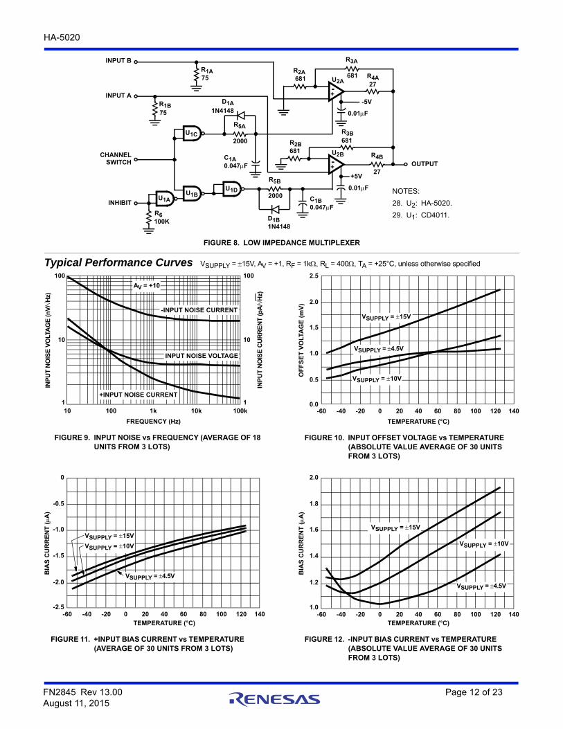
Low Impedance Multiplexer
Two common problems surface when you try to multiplex multiple high speed signals into a low impedance source
such as an A/D converter. The first problem is the low source impedance which tends to make amplifiers oscillate and causes gain errors. The second problem is the multiplexer which supplies no gain, introduces all kinds of distortion and limits the frequency response. Using op amps which have an enable/disable function, such as the HA-5020, eliminates the multiplexer problems because the external mux chip is not needed, and the HA-5020 can drive low impedance (large capacitance) loads if a series isolation resistor is used.
Referring to Figure 9, both inputs are terminated in their characteristic impedance; 75 is typical for video applications. Since the drivers usually are terminated in their characteristic impedance the input gain is 0.5, thus the amplifiers, U2, are configured in a gain of +2 to set the circuit gain equal to one. Resistors R2 and R3 determine the amplifier gain, and if a different gain is desired R2 should be changed according to the equation G = (1 + R3/R2). R3 sets the frequency response of the amplifier so you should refer to the manufacturers data sheet before changing its value. R5, C1 and D1 are an asymmetrical charge/discharge time circuit which configures U1 as a break before make switch to prevent both amplifiers from being active simultaneously. If this design is extended to more channels the drive logic must be designed to be break before make. R4 is enclosed in the feedback loop of the amplifier so that the large open loop amplifier gain of U2 will present the load with a small closed loop output impedance while keeping the amplifier stable for all values of load capacitance.
The circuit shown in Figure 9 was tested for the full range of capacitor values with no oscillations being observed; thus, problem one has been solved. The frequency and gain characteristics of the circuit are now those of the amplifier and independent of any multiplexing action; thus, problem two has been solved. The multiplexer transition time is approximately 15s with the component values shown.
NOTES:
24. U1 is HA-5020.
25. All resistors in
26. S1 is break before make.
27. Use ground plane.
VIDEO INPUT #1
VIDEO INPUT #2
R175
R3681
R2681
R475
R52000
+-
U1A
U1BR975
R102000R7
681R8
681
R675
+5V IN +5V
0.1F 10F
-5V IN -5V
0.1F 10F
+
+
1
R11100
VIDEO OUTPUTTO 75 LOAD
+5VS1
2
3
ALL OFF
FIGURE 8. TWO CHANNEL HIGH IMPEDANCE MULTIPLEXER
FN2845 Rev 13.00 Page 11 of 23August 11, 2015
HA-5020
FIGURE 8. LOW IMPEDANCE MULTIPLEXER
INPUT B
+-
-5V
+-
+5V
INHIBIT
CHANNELSWITCH
INPUT A
R1A75
R1B75
D1A1N4148
U1C
U1AU1B
U1D
R6100K
R5A
2000
C1A0.047F
R5B
2000
D1B1N4148
R2A681
R3A
681 R4A27
0.01F
R2B681
R4B
27
R3B681
0.01F
OUTPUT
U2B
U2A
C1B0.047F
NOTES:
28. U2: HA-5020.
29. U1: CD4011.
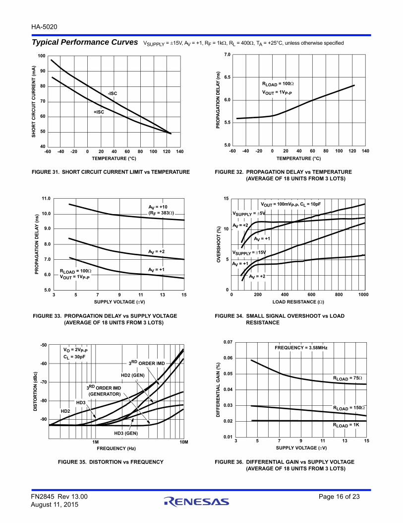
Typical Performance Curves VSUPPLY = 15V, AV = +1, RF = 1k RL = 400 TA = +25°C, unless otherwise specified
FIGURE 9. INPUT NOISE vs FREQUENCY (AVERAGE OF 18 UNITS FROM 3 LOTS)
FIGURE 10. INPUT OFFSET VOLTAGE vs TEMPERATURE (ABSOLUTE VALUE AVERAGE OF 30 UNITS FROM 3 LOTS)
FIGURE 11. +INPUT BIAS CURRENT vs TEMPERATURE (AVERAGE OF 30 UNITS FROM 3 LOTS)
FIGURE 12. -INPUT BIAS CURRENT vs TEMPERATURE (ABSOLUTE VALUE AVERAGE OF 30 UNITS FROM 3 LOTS)
FREQUENCY (Hz)
10 100 1k 10k 100k1
10
100
1
10
100
INP
UT
NO
ISE
VO
LTA
GE
(nV
/H
z)
INP
UT
NO
ISE
CU
RR
EN
T (p
A/
Hz)
AV = +10
-INPUT NOISE CURRENT
INPUT NOISE VOLTAGE
+INPUT NOISE CURRENT
TEMPERATURE (°C)
-60 -40 -20 0 20 40 60 80 100 120 140
OF
FS
ET
VO
LTA
GE
(m
V)
2.5
2.0
1.5
1.0
0.5
0.0
VSUPPLY = 15V
VSUPPLY = 4.5V
VSUPPLY = 10V
TEMPERATURE (°C)
-60 -40 -20 0 20 40 60 80 100 120 140
0
-0.5
-1.0
-1.5
-2.0
-2.5
VSUPPLY = 15V
VSUPPLY = 4.5V
VSUPPLY = 10V
BIA
S C
UR
RE
NT
(A
)
TEMPERATURE (°C)-60 -40 -20 0 20 40 60 80 100 120 140
BIA
S C
UR
RE
NT
(A
)
2.0
1.8
1.6
1.4
1.2
1.0
VSUPPLY = 15V
VSUPPLY = 4.5V
VSUPPLY = 10V
FN2845 Rev 13.00 Page 12 of 23August 11, 2015

HA-5020
FIGURE 13. TRANSIMPEDANCE vs TEMPERATURE (AVERAGE OF 30 UNITS FROM 3 LOTS)
FIGURE 14. SUPPLY CURRENT vs SUPPLY VOLTAGE (AVERAGE OF 30 UNITS FROM 3 LOTS)
FIGURE 15. DISABLE SUPPLY CURRENT vs SUPPLY VOLTAGE(AVERAGE OF 30 UNITS FROM 3 LOTS)
FIGURE 16. SUPPLY CURRENT vs DISABLE INPUT VOLTAGE
FIGURE 17. DISABLE MODE FEEDTHROUGH vs FREQUENCY FIGURE 18. DISABLED OUTPUT LEAKAGE vs TEMPERATURE (AVERAGE OF 30 UNITS FROM 3 LOTS)
Typical Performance Curves VSUPPLY = 15V, AV = +1, RF = 1k RL = 400 TA = +25°C, unless otherwise specified
TEMPERATURE (°C)-60 -40 -20 0 20 40 60 80 100 120 140
OP
EN
LO
OP
GA
IN (
M
)
6
5
4
3
2
1
VSUPPLY = 15V
VSUPPLY = 4.5V
VSUPPLY = 10V
SUPPLY VOLTAGE (V)3
SU
PP
LY C
UR
RE
NT
(m
A)
5 7 9 11 13 15
4
5
6
7
8
125°C
25°C
-55°C
SUPPLY VOLTAGE (V)
3
SU
PP
LY C
UR
RE
NT
(m
A)
5 7 9 11 13 150
4
5
6
7
125°C
25°C
-55°C
1
2
3
DISABLE = 0V
DISABLE INPUT VOLTAGE (V)
1 3 5 7 9 11 13 15
SU
PP
LY C
UR
RE
NT
(m
A)
5
4
3
2
1
0
6
7
8
9
VSUPPLY = 15VVSUPPLY = 4.5V VSUPPLY = 10V
0
-10
-20
-30
-40
-50
-60
-70
-80
FE
ED
TH
RO
UG
H (
dB
)
0 2M 4M 6M 8M 12M 14M10M 16M 18M 20M
FREQUENCY (Hz)
DISABLE = 0VVIN = 5VP-PRF = 750
TEMPERATURE (°C)
-60 -40 -20 0 20 40 60 80 100 120 140
OU
TP
UT
LE
AK
AG
E C
UR
RE
NT
(A
)
1.0
0.5
0
-0.5
-1.0
VOUT = +10V
VOUT = -10V
FN2845 Rev 13.00 Page 13 of 23August 11, 2015

HA-5020
FIGURE 19. ENABLE/DISABLE TIME vs OUTPUT VOLTAGE(AVERAGE OF 9 UNITS FROM 3 LOTS)
FIGURE 20. NON-INVERTING GAIN vs FREQUENCY
FIGURE 21. INVERTING FREQUENCY RESPONSE FIGURE 22. PHASE vs FREQUENCY
FIGURE 23. BANDWIDTH AND GAIN PEAKING vs LOADRESISTANCE
FIGURE 24. BANDWIDTH AND GAIN PEAKING vs FEEDBACK RESISTANCE
Typical Performance Curves VSUPPLY = 15V, AV = +1, RF = 1k RL = 400 TA = +25°C, unless otherwise specified
OUTPUT VOLTAGE (V)
-10 -8 -6 -4 -2 0 2 4 6 8 10
EN
AB
LE
TIM
E (s
)
2.0
1.6
1.2
0.8
0.4
0.0
1.8
1.4
1.0
0.6
0.2
DIS
AB
LE
TIM
E (s
)
20
16
12
8
4
0
18
14
10
6
2
ENABLE TIME
DISABLE TIME
FREQUENCY (Hz)
0 24M 48M 72M 96M 120M-7
-6
-5
-4
-3
-2
-1
0
1
2
3
NO
RM
AL
IZE
D G
AIN
(d
B)
VOUT = 0.2VP-P
CL = 10pF
AV = +1
AV = +2
AV = +6
AV = +10
FREQUENCY (Hz)
0 24M 48M 72M 96M 120M
-7
-6
-5
-4
-3
-2
-1
0
1
2
NO
RM
AL
IZE
D G
AIN
(d
B)
VOUT = 0.2VP-P
CL = 10pF
AV = -1
AV = -2
AV = -6AV = -10
RF = 750
-8
FREQUENCY (Hz)
0 24M 48M 72M 96M 120M
-225
-180
-135
-90
-45
0
+45
AV = -1AV = -2
AV = -6
AV = -10
-270
-135
-90
-45
+45
+90
+135
+180
-180
0
INV
ER
TIN
G P
HA
SE
(°)
NO
N-IN
VE
RT
ING
PH
AS
E (°
)
AV = +1
AV = +2
AV = +6
AV = +10
LOAD RESISTANCE ()
-3d
B B
AN
DW
IDT
H (
MH
z)
GA
IN P
EA
KIN
G (
dB
)
0 200 400 600 800 100060
70
80
90
100
110
0
1
2
3
4
5
GAIN PEAKING
-3dB BANDWIDTHCL = 10pF
VOUT = 0.2VP-P
FEEDBACK RESISTOR ()
700 900 1.1k 1.3k 1.5k85
90
95
100
105
0
5
10
15
20
-3d
B B
AN
DW
IDT
H (
MH
z)
GA
IN P
EA
KIN
G (
dB
)
GAIN PEAKING
-3dB BANDWIDTH
CL = 10pF
VOUT = 0.2VP-P
FN2845 Rev 13.00 Page 14 of 23August 11, 2015

HA-5020
FIGURE 25. BANDWIDTH AND GAIN PEAKING vs FEEDBACK RESISTANCE
FIGURE 26. BANDWIDTH vs FEEDBACK RESISTANCE
FIGURE 27. REJECTION RATIOS vs TEMPERATURE(AVERAGE OF 30 UNITS FROM 3 LOTS)
FIGURE 28. REJECTION RATIOS vs FREQUENCY
FIGURE 29. OUTPUT SWING OVERHEAD vs TEMPERATURE(AVERAGE OF 30 UNITS FROM 3 LOTS)
FIGURE 30. OUTPUT VOLTAGE SWING vs LOAD RESISTANCE
Typical Performance Curves VSUPPLY = 15V, AV = +1, RF = 1k RL = 400 TA = +25°C, unless otherwise specified
FEEDBACK RESISTOR ()400 600 800 1.0k 1.2k
80
85
90
95
100
-3d
B B
AN
DW
IDT
H (
MH
z)
GAIN PEAKING
-3dB BANDWIDTH
CL = 10pF, AV = +2
VOUT = 0.2VP-P
0
5
10
15
20
GA
IN P
EA
KIN
G (
dB
)
FEEDBACK RESISTOR ()
200 400 600 800 1000
40
50
60
70
80
-3d
B B
AN
DW
IDT
H (
MH
z)
GAIN PEAKING = 0dB
CL = 10pF, AV = +10VOUT = 0.2VP-P
30
20
10
TEMPERATURE (°C)
-60 -40 -20 0 20 40 60 80 100 120 140
RE
JEC
TIO
N R
AT
IO (d
B)
75
70
65
60
55
PSRR
CMRR
FREQUENCY (Hz)
10k 100k 1M 10M
RE
JEC
TIO
N R
AT
IO (d
B)
-50
-60
-70
-80
-90
+PSRR
CMRR
-40
-30
-20
-10
0
-PSRR
AV = +10
TEMPERATURE (°C)
OU
TP
UT
SW
ING
OV
ER
HE
AD
(V
)
1.5
2.0
2.5
3.0
3.5
0-20-40-60 80 100 120 140604020
VSUPPLY = 15V
VSUPPLY = 4.5V
VSUPPLY = 10V
(VSUPPLY) - (VOUT)
LOAD RESISTANCE ()
OU
TP
UT
VO
LTA
GE
SW
ING
(VP
-P)
10
15
20
25
30
10k1k10010
5
0
VSUPPLY = 15V
VSUPPLY = 4.5V
VSUPPLY = 10V
FN2845 Rev 13.00 Page 15 of 23August 11, 2015
HA-5020
FIGURE 31. SHORT CIRCUIT CURRENT LIMIT vs TEMPERATURE FIGURE 32. PROPAGATION DELAY vs TEMPERATURE(AVERAGE OF 18 UNITS FROM 3 LOTS)
FIGURE 33. PROPAGATION DELAY vs SUPPLY VOLTAGE(AVERAGE OF 18 UNITS FROM 3 LOTS)
FIGURE 34. SMALL SIGNAL OVERSHOOT vs LOADRESISTANCE
FIGURE 35. DISTORTION vs FREQUENCY FIGURE 36. DIFFERENTIAL GAIN vs SUPPLY VOLTAGE(AVERAGE OF 18 UNITS FROM 3 LOTS)
Typical Performance Curves VSUPPLY = 15V, AV = +1, RF = 1k RL = 400 TA = +25°C, unless otherwise specified
TEMPERATURE (°C)
-60 -40 -20 0 20 40 60 80 100 120 14040
50
60
70
80
90
100
SH
OR
T C
IRC
UIT
CU
RR
EN
T (
mA
)
-ISC
+ISC
TEMPERATURE (°C)
-60 -40 -20 0 20 40 60 80 100 120 140
PR
OP
AG
AT
ION
DE
LA
Y (n
s)
7.0
6.5
6.0
5.5
5.0
RLOAD = 100
VOUT = 1VP-P
SUPPLY VOLTAGE (V)
3 5 7 9 11 13 155.0
6.0
7.0
8.0
9.0
10.0
11.0
PR
OP
AG
AT
ION
DE
LA
Y (
ns
)
AV = +10(RF = 383)
RLOAD = 100VOUT = 1VP-P
AV = +2
AV = +1
LOAD RESISTANCE ()
OV
ER
SH
OO
T (%
)
10
15
10008006000
5
0400200
VOUT = 100mVP-P, CL = 10pF
VSUPPLY = 15V
VSUPPLY = 5V
AV = +2
AV = +1
AV = +1
AV = +2
FREQUENCY (Hz)
1M 10M
DIS
TO
RT
ION
(dB
c)
-50
-60
-70
-80
-90
HD2
VO = 2VP-P
CL = 30pF
HD3
HD3 (GEN)
HD2 (GEN)
3RD ORDER IMD
3RD ORDER IMD(GENERATOR)
SUPPLY VOLTAGE (V)
3 5 7 9 11 13 15
DIF
FE
RE
NT
IAL
GA
IN (
%)
0.01
0.02
0.03
0.04
0.05
0.06
0.07
RLOAD = 1K
RLOAD = 150
RLOAD = 75
FREQUENCY = 3.58MHz
FN2845 Rev 13.00 Page 16 of 23August 11, 2015

HA-5020
FIGURE 37. DIFFERENTIAL PHASE vs SUPPLY VOLTAGE(AVERAGE OF 18 UNITS FROM 3 LOTS)
FIGURE 38. SLEW RATE vs TEMPERATURE(AVERAGE OF 30 UNITS FROM 3 LOTS)
Typical Performance Curves VSUPPLY = 5V, AV = +1, RF = 1k RL = 400 TA = 25°C, Unless Otherwise Specified
FIGURE 39. NON-INVERTING FREQUENCY RESPONSE FIGURE 40. INVERTING FREQUENCY RESPONSE
FIGURE 41. PHASE RESPONSE AS A FUNCTION OF FREQUENCY
FIGURE 42. BANDWIDTH AND GAIN PEAKING vs FEEDBACK RESISTANCE
Typical Performance Curves VSUPPLY = 15V, AV = +1, RF = 1k RL = 400 TA = +25°C, unless otherwise specified
SUPPLY VOLTAGE (V)3 5 7 9 11 13 15
DIF
FE
RE
NT
IAL
PH
AS
E (
°)
0.01
0.02
0.03
0.04
0.05
0.06
0.07
RLOAD = 1K
RLOAD = 150
RLOAD = 75
FREQUENCY = 3.58MHz1200
1000
800
600-60
SL
EW
RA
TE
(V
/s
)
-40 -20 0 20 40 60 80 100 120 140
+SLEW RATE
-SLEW RATE
VOUT = 20VP-P
TEMPERATURE (°C)
5
4
3
2
1
0
-1
-2
-3
-4
-52M 10M 100M 200M
FREQUENCY (Hz)
NO
RM
AL
IZE
D G
AIN
(d
B)
AV + 2
AV + 10
AV + 1
5
4
3
2
1
0
-1
-2
-3
-4
-52M 10M 100M 200M
FREQUENCY (Hz)
NO
RM
AL
IZE
D G
AIN
(d
B)
AV = -1
AV = -2
AV = -10
5
4
3
2
1
0
-1
-2
-3
-4
-52M 10M 100M 200M
FREQUENCY (Hz)
AV + 1
AV - 1
AV - 10
AV + 10
INV
ER
TIN
G P
HA
SE
(°)
180
135
90
45
0
-45
-90
-135
-180
NO
N-I
NV
ER
TIN
G P
HA
SE
(°)
FEEDBACK RESISTOR ()
500 700 900 1100 1300 1500
140
130
120 10
5
0
-3d
B B
AN
DW
IDT
H (
MH
z)
GA
IN P
EA
KIN
G (
dB
)
VOUT = 0.2VP-PCL = 10pF
-3dB BANDWIDTH
GAIN PEAKING
AV = +1
FN2845 Rev 13.00 Page 17 of 23August 11, 2015
HA-5020
FIGURE 43. BANDWIDTH AND GAIN PEAKING vs FEEDBACK RESISTANCE
FIGURE 44. BANDWIDTH AND GAIN PEAKING vs LOAD RESISTANCE
FIGURE 45. BANDWIDTH vs FEEDBACK RESISTANCE FIGURE 46. REJECTION RATIOS vs FREQUENCY
FIGURE 47. PROPAGATION DELAY vs TEMPERATURE FIGURE 48. SLEW RATE vs TEMPERATURE
Typical Performance Curves VSUPPLY = 5V, AV = +1, RF = 1k RL = 400 TA = 25°C, Unless Otherwise Specified (Continued)
FEEDBACK RESISTOR ()
-3d
B B
AN
DW
IDT
H (
MH
z)
GA
IN P
EA
KIN
G (
dB
)
100
95
90
0
350 500 650 800 950 1100
-3dB BANDWIDTH
GAIN PEAKING
VOUT = 0.2VP-PCL = 10pFAV = +2
5
10
LOAD RESISTOR ()
-3d
B B
AN
DW
IDT
H (
MH
z)
GA
IN P
EA
KIN
G (
dB
)
130
120
110
100
90
800 200 400 600 800 1000
6
4
2
0
VOUT = 0.2VP-PCL = 10pF
-3dB BANDWIDTH
GAIN PEAKING
AV = +1
80
60
40
20
0200 350 500 650 800 950
-3d
B B
AN
DW
IDT
H (
MH
z)
FEEDBACK RESISTOR ()
VOUT = 0.2VP-PCL = 10pFAV = +10
FREQUENCY (Hz)
0
-10
-20
-30
-40
-50
-60
-70
-80
RE
JEC
TIO
N R
AT
IO (
dB
)
0.001M 0.01M 0.1M 1M 10M 30M
AV = +1
CMRR
POSITIVE PSRR
NEGATIVE PSRR
TEMPERATURE (°C)
-50 -25 0 25 50 75 100 125
8.0
7.5
7.0
6.5
6.0
PR
OP
AG
AT
ION
DE
LA
Y (
ns)
RL = 100VOUT = 1.0VP-PAV = +1
TEMPERATURE (°C)
-50 -25 0 25 50 75 100 125
500
450
400
350
300
250
200
150
100
SL
EW
RA
TE
(V
/s
)
VOUT = 2VP-P
+ SLEW RATE
- SLEW RATE
FN2845 Rev 13.00 Page 18 of 23August 11, 2015

HA-5020
FIGURE 49. NON-INVERTING GAIN FLATNESS vs FREQUENCY FIGURE 50. INVERTING GAIN FLATNESS vs FREQUENCY
FIGURE 51. INPUT NOISE CHARACTERISTICS FIGURE 52. REJECTION RATIO vs TEMPERATURE
FIGURE 53. OUTPUT SWING vs TEMPERATURE FIGURE 54. ENABLE/DISABLE TIME vs OUTPUT VOLTAGE
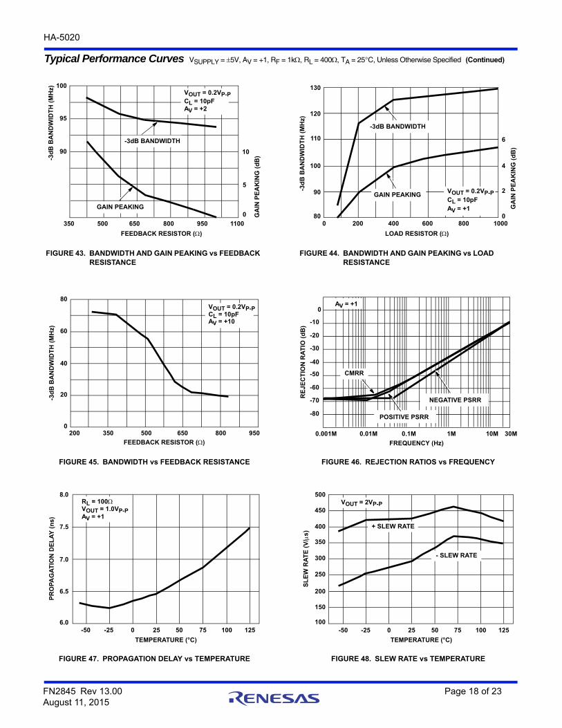
Typical Performance Curves VSUPPLY = 5V, AV = +1, RF = 1k RL = 400 TA = 25°C, Unless Otherwise Specified (Continued)
FREQUENCY (Hz)
5M 10M 15M 20M 25M 30M
0.8
0.6
0.4
0.2
0
-0.2
-0.4
-0.6
-0.8
-1.0
-1.2
NO
RM
AL
IZE
D G
AIN
(d
B)
VOUT = 0.2VP-PCL = 10pF
AV = +2, RF = 681
AV = +5, RF = 1k
AV = +1, RF = 1k
AV = 10, RF = 383
0.8
0.6
0.4
0.2
0
-0.2
-0.4
-0.6
-0.8
-1.0
-1.2
NO
RM
AL
IZE
D G
AIN
(d
B)
FREQUENCY (Hz)
5M 10M 15M 20M 25M 30M
AV = -1
AV = -2
AV = -5
AV = -10
VOUT = 0.2VP-PCL = 10pF
RF = 750
FREQUENCY (Hz)
0.01k 0.1k 1k 10k 100k
VO
LTA
GE
NO
ISE
(n
V/
Hz)
CU
RR
EN
T N
OIS
E (
pA
/H
z)
100
80
60
40
20
0
1000
800
600
400
200
0
AV = 10, RF = 383
-INPUT NOISE CURRENT
+INPUT NOISE CURRENT
+INPUT NOISE VOLTAGE
58
60
62
64
66
68
70
72
74
-100 -50 0 50 100 150
+PSRR
-PSRR
CMRR
200 250
TEMPERATURE (°C)
RE
JE
CT
ION
RA
TIO
(d
B)
4.0
3.8
3.6-60 -40 -20 0 40 60 80 100 120 14020
TEMPERATURE (°C)
OU
TP
UT
SW
ING
(V
)
DISABLE
ENABLE
ENABLE
DISABLE
EN
AB
LE
TIM
E (
ns
)
20
18
16
14
12
10
8
6
4
2
0
OUTPUT VOLTAGE (V)
-2.5 -2.0 -1.5 -1.0 -0.5 0 0.5 1.0 1.5 2.0 2.5
32
30
28
26
24
22
20
18
16
14
12
DIS
AB
LE
TIM
E (s
)
FN2845 Rev 13.00 Page 19 of 23August 11, 2015
HA-5020
About IntersilIntersil Corporation is a leading provider of innovative power management and precision analog solutions. The company's products address some of the largest markets within the industrial and infrastructure, mobile computing and high-end consumer markets.
For the most updated datasheet, application notes, related documentation and related parts, please see the respective product information page found at www.intersil.com.
You may report errors or suggestions for improving this datasheet by visiting www.intersil.com/ask.
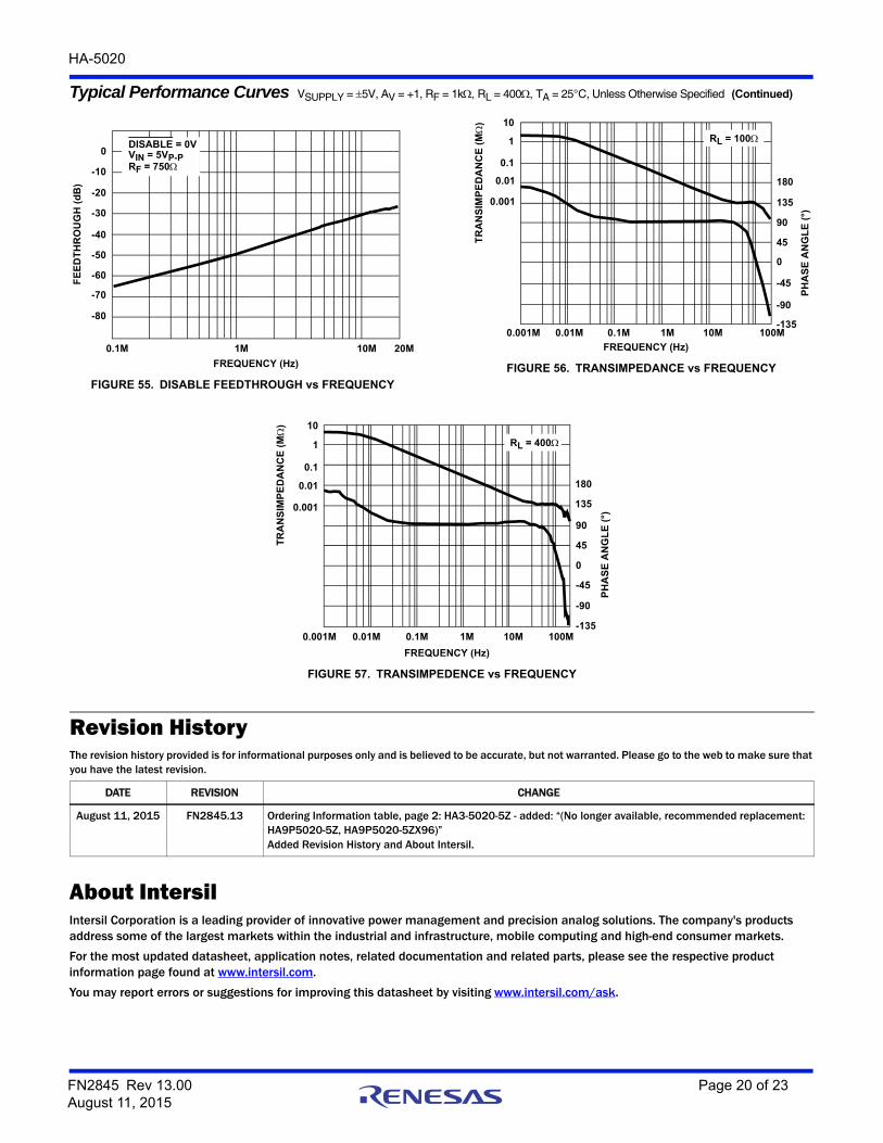
FIGURE 55. DISABLE FEEDTHROUGH vs FREQUENCY
FIGURE 56. TRANSIMPEDANCE vs FREQUENCY
FIGURE 57. TRANSIMPEDENCE vs FREQUENCY
Revision HistoryThe revision history provided is for informational purposes only and is believed to be accurate, but not warranted. Please go to the web to make sure that you have the latest revision.
DATE REVISION CHANGE
August 11, 2015 FN2845.13 Ordering Information table, page 2: HA3-5020-5Z - added: “(No longer available, recommended replacement: HA9P5020-5Z, HA9P5020-5ZX96)”Added Revision History and About Intersil.
Typical Performance Curves VSUPPLY = 5V, AV = +1, RF = 1k RL = 400 TA = 25°C, Unless Otherwise Specified (Continued)
-20
-40
-50
-60
-70
-80
0.1M 1M 10M 20M
FE
ED
TH
RO
UG
H (
dB
)
FREQUENCY (Hz)
-30
-10
0DISABLE = 0VVIN = 5VP-PRF = 750
-135
-90
-45
0
45
90
135
180
10
1
0.1
0.01
0.001
0.001M 0.01M 0.1M 1M 10M 100M
PH
AS
E A
NG
LE
(°)
TR
AN
SIM
PE
DA
NC
E (
M
)
RL = 100
FREQUENCY (Hz)
-135
-90
-45
0
45
90
135
180
10
1
0.1
0.01
0.001
0.001M 0.01M 0.1M 1M 10M 100M
PH
AS
E A
NG
LE
(°)
RL = 400
FREQUENCY (Hz)
TR
AN
SIM
PE
DA
NC
E (
M
)
FN2845 Rev 13.00 Page 20 of 23August 11, 2015
HA-5020
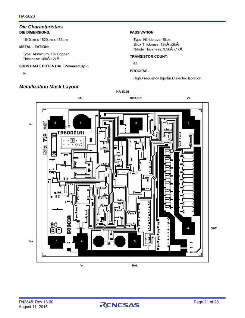
Die Characteristics
Metallization Mask LayoutHA-5020
DIE DIMENSIONS:
1640m x 1520m x 483m
METALLIZATION:
Type: Aluminum, 1% CopperThickness: 16kÅ 2kÅ
SUBSTRATE POTENTIAL (Powered Up):
V-
PASSIVATION:
Type: Nitride over SiloxSilox Thickness: 12kÅ 2kÅNitride Thickness: 3.5kÅ 1kÅ
TRANSISTOR COUNT:
62
PROCESS:
High Frequency Bipolar Dielectric Isolation
43
2 1 8 7
6
5IN+
IN-
OUT
BALV-
BAL DISABLE V+
FN2845 Rev 13.00 Page 21 of 23August 11, 2015

FN2845 Rev 13.00 Page 22 of 23August 11, 2015
HA-5020
Intersil products are manufactured, assembled and tested utilizing ISO9001 quality systems as notedin the quality certifications found at www.intersil.com/en/support/qualandreliability.html
Intersil products are sold by description only. Intersil may modify the circuit design and/or specifications of products at any time without notice, provided that such modification does not, in Intersil's sole judgment, affect the form, fit or function of the product. Accordingly, the reader is cautioned to verify that datasheets are current before placing orders. Information furnished by Intersil is believed to be accurate and reliable. However, no responsibility is assumed by Intersil or its subsidiaries for its use; nor for any infringements of patents or other rights of third parties which may result from its use. No license is granted by implication or otherwise under any patent or patent rights of Intersil or its subsidiaries.
For information regarding Intersil Corporation and its products, see www.intersil.com
For additional products, see www.intersil.com/en/products.html
© Copyright Intersil Americas LLC 2002-2015. All Rights Reserved.All trademarks and registered trademarks are the property of their respective owners.
Dual-In-Line Plastic Packages (PDIP)
CL
E
eA
C
eB
eC
-B-
E1INDEX
1 2 3 N/2
N
AREA
SEATING
BASEPLANE
PLANE
-C-
D1
B1B
e
D
D1
AA2
L
A1
-A-
0.010 (0.25) C AM B S
NOTES:
1. Controlling Dimensions: INCH. In case of conflict between English and Metric dimensions, the inch dimensions control.
2. Dimensioning and tolerancing per ANSI Y14.5M-1982.
3. Symbols are defined in the “MO Series Symbol List” in Section 2.2 of Publication No. 95.
4. Dimensions A, A1 and L are measured with the package seated in JEDEC seating plane gauge GS-3.
5. D, D1, and E1 dimensions do not include mold flash or protru-sions. Mold flash or protrusions shall not exceed 0.010 inch(0.25mm).
6. E and are measured with the leads constrained to be per-pendicular to datum .
7. eB and eC are measured at the lead tips with the leads uncon-strained. eC must be zero or greater.
8. B1 maximum dimensions do not include dambar protrusions. Dambar protrusions shall not exceed 0.010 inch (0.25mm).
9. N is the maximum number of terminal positions.
10. Corner leads (1, N, N/2 and N/2 + 1) for E8.3, E16.3, E18.3, E28.3, E42.6 will have a B1 dimension of 0.030 - 0.045 inch(0.76 - 1.14mm).
eA-C-
E8.3 (JEDEC MS-001-BA ISSUE D)8 LEAD DUAL-IN-LINE PLASTIC PACKAGE
SYMBOL
INCHES MILLIMETERS
NOTESMIN MAX MIN MAX
A - 0.210 - 5.33 4
A1 0.015 - 0.39 - 4
A2 0.115 0.195 2.93 4.95 -
B 0.014 0.022 0.356 0.558 -
B1 0.045 0.070 1.15 1.77 8, 10
C 0.008 0.014 0.204 0.355 -
D 0.355 0.400 9.01 10.16 5
D1 0.005 - 0.13 - 5
E 0.300 0.325 7.62 8.25 6
E1 0.240 0.280 6.10 7.11 5
e 0.100 BSC 2.54 BSC -
eA 0.300 BSC 7.62 BSC 6
eB - 0.430 - 10.92 7
L 0.115 0.150 2.93 3.81 4
N 8 8 9
Rev. 0 12/93

HA-5020
FN2845 Rev 13.00 Page 23 of 23August 11, 2015
Package Outline DrawingM8.15 8 LEAD NARROW BODY SMALL OUTLINE PLASTIC PACKAGE
Rev 4, 1/12
DETAIL "A"
TOP VIEW
INDEX
AREA
1 2 3
-C-
SEATING PLANE
x 45°
NOTES:1. Dimensioning and tolerancing per ANSI Y14.5M-1994.2. Package length does not include mold flash, protrusions or gate burrs.
Mold flash, protrusion and gate burrs shall not exceed 0.15mm (0.006inch) per side.
3. Package width does not include interlead flash or protrusions. Interlead flash and protrusions shall not exceed 0.25mm (0.010 inch) per side.
4. The chamfer on the body is optional. If it is not present, a visual indexfeature must be located within the crosshatched area.
5. Terminal numbers are shown for reference only.6. The lead width as measured 0.36mm (0.014 inch) or greater above the
seating plane, shall not exceed a maximum value of 0.61mm (0.024 inch).7. Controlling dimension: MILLIMETER. Converted inch dimensions are not
necessarily exact.8. This outline conforms to JEDEC publication MS-012-AA ISSUE C.
SIDE VIEW “A
SIDE VIEW “B”
1.27 (0.050)
6.20 (0.244)5.80 (0.228)
4.00 (0.157)3.80 (0.150)
0.50 (0.20)0.25 (0.01)
5.00 (0.197)4.80 (0.189)
1.75 (0.069)1.35 (0.053)
0.25(0.010)0.10(0.004)
0.51(0.020)0.33(0.013)
8°0°
0.25 (0.010)0.19 (0.008)
1.27 (0.050)
0.40 (0.016)
1.27 (0.050)
5.20(0.205)
1
2
3
4 5
6
7
8
TYPICAL RECOMMENDED LAND PATTERN
2.20 (0.087)
0.60 (0.023)