Embed Size (px)
Citation preview

GS66508P-E05 650V enhancement mode GaN transistor
PRELIMINARY DATASHEET
Preliminary – Rev 150223 © 2009-2015 GaN Systems Inc. 1 This information pertains to a product under development. Its characteristics and specifications are subject to change without notice.
Features
– 650V enhancement mode power switch – Ultra low FOM Island Technology™ die – Low inductance GaNPX™ package – Reverse current capability – Zero reverse recovery charge – Source-sense for optimal high speed design – RoHS 6 compliant
Applications – On-board battery chargers – 400V DC-DC conversion – Inverters, UPS, and VFD motor drive – AC-DC power supplies (PFC & primary) – VHF small form factor power adapters – High frequency, high efficiency power
conversion
Absolute Maximum Ratings (Tcase = 25˚C except as noted)
Parameters Symbol Value Units Operating Junction Temperature TJ -55 to +150 °C Storage Temperature Range TS -55 to +150 °C Drain-to-Source Voltage VDS 650 V Gate-to-Source Voltage VGS ±10 V Continuous Drain Current (Tcase=25°C) (Note 1) IDS(cont)25 30 A Continuous Drain Current (Tcase=100°C) IDS(cont)100 23 A Pulsed Drain Current (Tcase=25°C) (Note 2) ID‚pulse 60 A (1) Saturation imposes current limit. (2) Pulse width is limited by TJ(max).
Thermal Characteristics (Typical values unless otherwise noted)
Parameters Symbol Value Units Thermal Resistance (junction to case) RΘJC 0.5
°C /W Thermal Resistance (junction to ambient) (Note 3) RΘJA 51 Maximum Soldering Temperature (MSL3 rated) TSOLD 260 °C
(3) Device mounted on 40mm x 40mm x 1.5mm single layer epoxy PCB FR4 with 6cm2 copper area (thickness 70μm) for thermal pad
connection. PCB is vertical without air stream cooling. For optimized thermal designs, refer to Application Note GN005 “Thermal Analysis and PCB Design Guidelines for GaN Enhancement Mode Power Switching Transistors” .
Ordering Information
Part number Package type Ordering code Packing method Pack quantity GS66508P-E05 GaNPX GS66508P-E05-TY Tray 100
* TP = thermal pad. TP is internally connected to the substrate and must be connected externally to the source (S)
D
S
SS G
top view
TP*
D
S
G
SS

GS66508P-E05 650V enhancement mode GaN transistor
PRELIMINARY DATASHEET
Preliminary – Rev 150223 © 2009-2015 GaN Systems Inc. 2 This information pertains to a product under development. Its characteristics and specifications are subject to change without notice.
Electrical Characteristics (Typical values at Tcase= 25°C unless otherwise noted)
Parameters Symbol Min Typ Max Units Conditions (Note 4)
Drain-to-Source Breakdown Voltage BVDSS 650 V VGS =0V ID=1mA
Drain-to-Source On Resistance (TJ =25°C) RDS(ON)
55 mΩ VGS =7V, TJ=25°C ID=9A
Drain-to-Source On Resistance (TJ=150°C) 140 mΩ VGS =7V, TJ=150°C ID=9A
Gate Threshold Voltage VGS(th) 1.6 V VDS =VGS
ID=7mA
Drain to Source Leakage Current (TJ=25°C) IDSS
2 µA VDS=650V VGS =0V, TJ=25°C
Drain to Source Leakage Current (TJ=150°C) 400 µA VDS=650V VGS =0V, TJ=150°C
Gate to Source Current IGS 40 µA VGS=7V, VDS=0V TJ=25°C
Gate Resistance RG 1.5 Ω f=1MHz, open drain
Gate Plateau Voltage Vplat 3 V VDS=400V
Source-Drain Reverse Voltage VSD 2.8 V VGS=0V, TJ =25°C ISD = 9A
Input Capacitance CISS 200
pF VDS=400V
VGS=0V f=1MHz
Output Capacitance COSS 67
Reverse Transfer Capacitance CRSS 2.0
Effective Output Capacitance, Energy Related (Note 5) Co(er) 88 pF VGS =0V
VDS=0 to 400V
Effective Output Capacitance, Time Related (Note 6) Co(tr) 143 pF
ID =constant VGS =0V
VDS=0 to 400V
Total Gate Charge QG(TOT) 6.5 nC VGS=0 to 7V VDS=400V Gate-to-Source Charge QGS 1.4 nC
Gate-to-Drain Charge QGD 2.8 nC
Reverse Recovery Charge QRR 0 nC
Output Charge QOSS 57 nC VGS=0V VDS=400V
(4) All parameters are specified with the substrate and thermal pad connected to the source (5) Co(er) is the fixed capacitance that would give the same stored energy as COSS while VDS is rising from 0V to the stated VDS (6) Co(tr) is the fixed capacitance that would give the same charging time as COSS while VDS is rising from 0V to the stated VDS
GS66508P-E05 650V enhancement mode GaN transistor
PRELIMINARY DATASHEET
Preliminary – Rev 150223 © 2009-2015 GaN Systems Inc. 3 This information pertains to a product under development. Its characteristics and specifications are subject to change without notice.
Package Dimensions
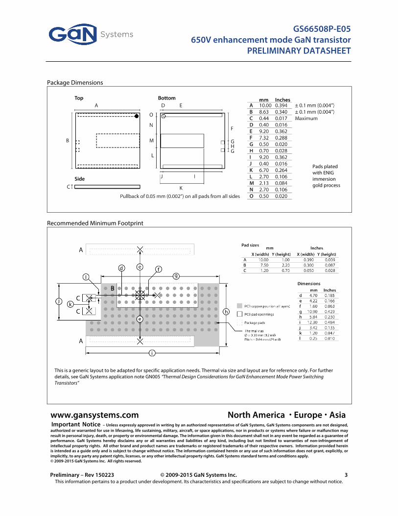
Recommended Minimum Footprint
www.gansystems.com North America � Europe � Asia
Important Notice – Unless expressly approved in writing by an authorized representative of GaN Systems, GaN Systems components are not designed, authorized or warranted for use in lifesaving, life sustaining, military, aircraft, or space applications, nor in products or systems where failure or malfunction may result in personal injury, death, or property or environmental damage. The information given in this document shall not in any event be regarded as a guarantee of performance. GaN Systems hereby disclaims any or all warranties and liabilities of any kind, including but not limited to warranties of non-infringement of intellectual property rights. All other brand and product names are trademarks or registered trademarks of their respective owners. Information provided herein is intended as a guide only and is subject to change without notice. The information contained herein or any use of such information does not grant, explicitly, or implicitly, to any party any patent rights, licenses, or any other intellectual property rights. GaN Systems standard terms and conditions apply. © 2009-2015 GaN Systems Inc. All rights reserved.
Pads plated with ENIG immersion gold process
This is a generic layout to be adapted for specific application needs. Thermal via size and layout are for reference only. For further details, see GaN Systems application note GN005 “Thermal Design Considerations for GaN Enhancement Mode Power Switching Transistors”

Mouser Electronics
Authorized Distributor
Click to View Pricing, Inventory, Delivery & Lifecycle Information: GaN Systems:
GS66508P-E05-TY GS66508P-E05-MR
![Penentuan Selfheating Pada Sensor Suhu Rendah Lapisan ......pada kaji an komputasi model termal arus statis pada transistor seperti transistor AlGaN/GaN [1] karena dapat mempengaruhi](https://img.dokumen.tips/doc/110x75/6090314d9280f07f0c7adfc4/penentuan-selfheating-pada-sensor-suhu-rendah-lapisan-pada-kaji-an-komputasi.jpg)