Embed Size (px)
DESCRIPTION
False top coatings of a counterfeit component revealed layer by layer; Wafer-level solder sphere placement and its implications; Steps toward closing the software reliability gap
Citation preview

The Global Assembly Journal for SMT and Advanced Packaging Professionals
Volume 10 Number 7 July 2010
ISSN 1474 - 0893
www.globalsmt.net
The Global Assembly Journal for SMT and Advanced Packaging Professionals
ISSN 1474 - 0893
David RabyInterview Inside
NEW PRODUCTS
INDUSTRY NEWS
INTERNATIONAL DIARY
False top coatings oF a counterFeit component revealed layer by layer
WaFer-level solder sphere placement and its implications
steps toWard closing the soFtWare quality gap
David RabyInterview Inside
NEW PRODUCTS
INDUSTRY NEWS
INTERNATIONAL DIARY
False top coatings oF a counterFeit component revealed layer by layer
WaFer-level solder sphere placement and its implications
steps toWard closing the soFtWare quality gap
Volume 10 Number 7 July 2010

Global SMT & Packaging – Celebrating 10 Years – July 2010 – 1www.globalsmt.net
Contents
ContentsGlobal SMT & Packagingis distributed by controlled
circulation to qualified personnel. For all others, sub-
scriptions are available at a cost of £181.50 for the
current volume (twelve issues).
No part of this publication may be reproduced, stored in a
retrieval system, transmitted in any form or by any means
electronic, mechanical, photocopying, recording or
otherwise without prior writ-ten consent of the publisher.
No responsibility is accepted for the accuracy of information
contained in the text, illustrations or advertisements. The opinions expressed in the
articles are not necessarily those of the editors or publisher.
ISSN No. 1474-0893© Trafalgar Publications Ltd
Designed and Published byTrafalgar Publications Ltd,
Bournemouth, United Kingdom
Printed by Ovid Bell,Fulton, MO, USA.
Volume 10, No. 7
July 2010
European edition
2 Foxconn and the power of tier one EMS companies Trevor Galbraith
TechNology Focus
10 False top coatings of a counterfeit component revealed layer by layer
Art Ogg, World Micro
14 Wafer-level solder sphere placement and its implications Andrew Strandjord, Thomas Oppert, Thorsten Teutsch, and
Ghassem Azdasht, PacTech—Packaging Technologies, Inc.
26 Steps toward closing the software quality gap Frederick R. Hume, Data I/O Corporation, and Mary Beth
Soloy, Ford Motor Company
special FeaTures
30 Interview—David Raby, STI Electronics32 Show report: SMT/HYBRID/PACKAGING rises above the ashes
REGULAR COLUMNS
4 Desoldering braid/solder wick Bob Willis
20 Strong global growth throughout supply chain Walt Custer and Jon Custer-Topai
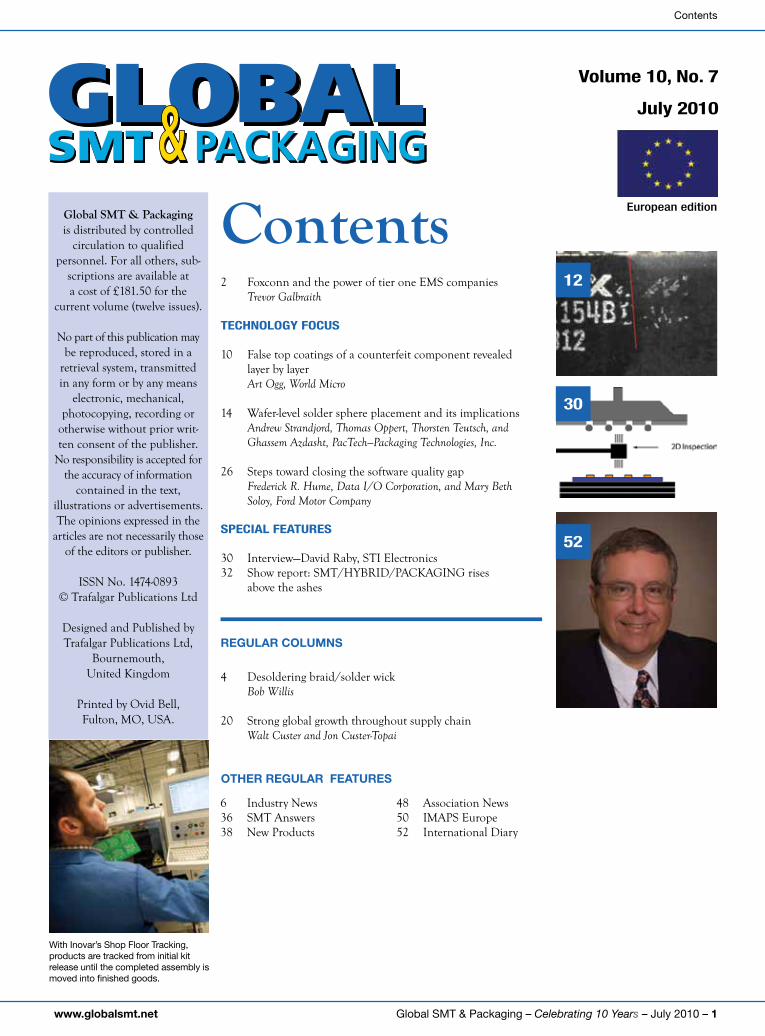
With Inovar’s Shop Floor Tracking, products are tracked from initial kit release until the completed assembly is moved into finished goods.
52
6 Industry News36 SMT Answers38 New Products
48 Association News50 IMAPS Europe52 International Diary
12
OThER REGULAR FEATURES
30
2 – Global SMT & Packaging – Celebrating 10 Years – July 2010 www.globalsmt.net
Editorial
Trevor GalbraithEditor-in-Chief
Editorial OfficesEuropeGlobal SMT & PackagingTrafalgar Publications LtdUnit 18, 2 Lansdowne CrescentBournemouthDorset BH1 1SAUnited KingdomTel: +44 (1202) 388997E-mail: [email protected]: www.globalsmt.net
United StatesGlobal SMT & PackagingPO Box 7579Naples, FL 34102, USATel: +1 (239) 245-9264Fax: (239) 236-4682E-mail: [email protected]
ChinaGlobal SMT & PackagingElectronics SecondResearch InstituteNo.159, Hepin South RoadTaiyuan City, PO Box 115, Shanxi,Province 030024, ChinaTel: +86 (351) 652 3813Fax: +86 (351) 652 0409
Editor-in-ChiefTrevor GalbraithTel: +44 (0)20 8123 6704 (Europe)Tel: +1 (239) 245-9264 x101 (US)E-mail: [email protected]
Managing EditorHeather LackeyTel: +1 (239) 245-9264 x105E-mail: [email protected]
Circulation & SubscriptionsKelly Grimm Tel: +1 (239) 245-9264 x106E-mail: [email protected]
AdvertisingGlobal SMT & Packaging offers effective print, web, email and video advertising opportunities. Contact your local sales rep today.
Americas—Derek Laborie (print & video)Tel: +1 (239) 245-9264 x102Mobile: +1 (603) [email protected]
Sandy Daneau (digital)Tel: +1 (239) 245-9264 x104 Cell: +1 (603)[email protected]
Europe—Andy KellardTel: +44 7766 [email protected]
Asia/Pacific— Debasish P. ChoudhuryTel: +91 120 [email protected]
Nitesh [email protected]
Asia— Carol [email protected]
There have been many column inches expounded on the recent suicides at Foxconn plants, particularly in their South China facility in Shenzhen. While these deaths are tragic, if you compare the number of suicides to the national average per capita, then the Foxconn deaths actually fall below the national average.
This is not to say that working and living condition in a Foxconn plant are any great shakes, but the bigger story is the ramifications these sensationalist headlines produce.
Not four months ago there was an incident in Juarez where some workers were wrongly told the bus was not available at the end of their shift to take them into town. When one suspicious worker walked outside to verify this and found they had been lied to, a small riot ensued and they started a bonfire at the end of one of the production lines. The negative press was quickly followed by an announcement from Foxconn corporate about their intention to revive attempts to build the industry’s first ‘lights-out” factory.
The furor over the suicide jumpers produced another strong reaction from the world’s largest CEM. It started with announcement to double factory workers salaries to around $132 per month. This in itself was a little suspicious. According to the company, this will add 10-12% to the bottom line, but what about these razor thin profit margins of 2-3% we keep hearing about?
Nevertheless, it was a generous response to a baying global public that was starting to impact on their biggest customer, Apple. Steve Jobs was duly dispatched to Shenzhen and did a less than convincing PR job. The next step by the EMS giant was more menacing—according
to recent reports, they are planning to move the majority of their manufacturing outside of China.
Even to a country the size of China, this is a serious threat. 400,000 workers would be laid-off, making the difficult job the Chinese government has containing social unrest even harder.
This reminded me of the time when Hungary applied for membership of the European Union. A condition of membership was to stop all the capital gains and other tax incentives they offered foreign companies for inward investment. At the time, the biggest reaction came from Flextronics who were the country’s biggest employer. They threatened to pull-out if these rules were implemented and the country was forced to go back to the European Union and negotiate a more acceptable phase-out of these incentives over ten years.
The power of tier one manufacturers should not be underestimated. Given the number of jobs (albeit low-paid and sometimes in less than desirable conditions), the taxes paid and the spending power of the employees back into the local economy, they make a significant contribution.
Notwithstanding the strange number surrounding the recently announced wage hike in Southern China, tier one manufacturers perform a very necessary job in very demanding conditions. These conditions are not set by themselves, or even their customers, but by us, the consumer. The constant goal of smaller, faster, cheaper looks like it may finally be finding its lowest point.
—Trevor Galbraith.
Foxconn and the power of tier one EMS companies
Correction: Dr. George Riley, author of the article “New Opportunities for Controlling Pressure in Flip Chip Assembly,” printed in our March issue, is employed by flipchips.com and not Sensor Products Inc.

Henkel – Materials Partner of Choice for the Electronics IndustryNo matter where you are or what your process requires, you can count on Henkel’s expertise. Our unmatched portfolio of advanced materials for the semiconductor and assembly markets, all backed by the innovation, knowledge and support of Henkel’s world-class global team, ensures your success and guarantees a low-risk partnership proposition.

Title
4 – Global SMT & Packaging – Celebrating 10 Years – July 2010 www.globalsmt.net
Bob Willis
Desoldering braid/solder wick
Solder wick or braid is supplied in two forms, tin plated or plain copper woven braid which is impregnated with flux. Today the bare copper option is the most popular and most often seen in production. The flux coating helps provide protection to the copper braid during storage and helps the solder wet the braid and capillary quickly during soldering. If is often seen in production that braid held in an operator’s toolbox does not have the same wicking or capillary action during desoldering. This is due to the copper braid ageing, so don’t lock it away or order a large stock to save money—new is best!! Also, don’t let braid supported with liquid flux become part of your standard shop floor operation!!
Copper is the preferred braid as it is far easier to see soldering, or rather the desoldering action, taking place. The solder can be seen to wick up into the braid when new material is used along with the correct gauge. It also provides a simple guide to the solderability or the age of the braid being used.
Desoldering single-sided through hole joints with copper braidSolder braid is used in two main applications during assembly:• On conventional through hole boards
for solder short removal and on single-sided, non-plated through hole boards for desoldering terminations. Heated vacuum desoldering systems, however, are the preferred method for professional desoldering of plated through hole boards
• For the removal of solder from surface mount and area array pads after component removal or during solder short removal on SOIC or on other fine pitch components.
The basic method for using braid is as follows:
Solder short removal on through hole and surface mount component terminations.
Select a braid width the same size or slightly smaller than the short being removed. This allows the desoldering operation to be seen. It also reduces the heat input required to allow the solder to
reflow. Clean and tin the iron bit, making sure
the bit is the correct size and temperature. Normally the tip temperature would be 600˚Fforworkonprintedcircuitboards.The size of the tip would be the same size as the braid width. Before desoldering, make sure the end of the braid is free from solder. The more braid and solder in contact will affect the time to reflow or the time required on the joint area for all the solder to be removed.
Apply the braid onto the surface of the solder short and place the iron tip on to the braid. By tinning the bit the solder on the tip will speed up heat transfer to the braid and the whole desoldering operation. This is often where damage occurs, when operators do not tin the bit and try to speed up heat transfer by applying pressure to the braid that is not necessary. When the solder becomes a liquid, it will wet up the braid by capillary action, but also based on the type and age of the braid.
After the solder short has been removed from the joint, check that the solder remaining on the adjacent joints
Desoldering braid/ solder wick May be low tech but still vital in rework and repair areas
Figure 1. Manual desoldering using solder braid.

Global SMT & Packaging – Celebrating 10 Years – July 2010 – 5www.globalsmt.net
Desoldering braid/solder wick
meets your inspection standard. If it does not, resolder the terminations to meet the standard requirements
Desoldering non-plated through hole jointsSelect a braid width the same size or slightly smaller than the solder joint being desoldered. This allows the desoldering operation to be seen it also reduces the heat input required to allow the solder to reflow. Clean and tin the bit on the iron making sure the bit is the correct size and temperature. Normally the tip temperature would be 600F for work on printed circuit boards. The size of the tip would be the same size as the braid width.
Before desoldering make sure the end of the braid is free from solder. The more braid and solder in contact will either affect the time to reflow or the time required on the joint area for all the solder to be removed. Staff are often observed on the shop floor using a solder loaded braid tail several inches long before cutting the braid tail off.
Apply the braid onto the surface of the solder joint and place the iron tip on to the braid. By tinning the bit, the solder on the tip will speed up heat transfer to the braid and the whole de-soldering operation. This is often where damage occurs, when operators do not tin the bit and instead try to speed up heat transfer by applying unnecessary pressure to the braid.
It is relatively simple to see solder left between surface pads, normally referred to as sweat joints.
After the solder has been removed from the joint, check that the leads of the component are free from the pads and that no damage is visible on the pads. Using tweezers or snip-nose pliers should allow the leads to move freely in the hole. When all leads have been checked the component
may be removed. If all leads have been correctly desoldered, no damage can occur on the pads.
solder removal from surface mount padsIn the first place, only remove solder from surface mount pads when it is really necessary. In most cases it is not. It is, however, for many fine pitch and all BGA applications due to the difficulty of replacing the new components or printing paste onto the repair site.
Select a braid width the same size or slightly smaller than the pad being reworked. This allows the desoldering operation to be seen; it also reduces the heat input required to allow the solder to reflow.
Clean and tin the bit on the iron ensuring the bit is the correct size and temperature. Normally the tip temperature wouldbe600˚Fforworkonprintedcircuit boards. The size of the tip would be the same as the braid width or slightly smaller.
Before desoldering, ensure the end of the braid is free from solder. The more braid and solder in contact with the pad will affect the time to reflow or the time required on the pad area during solder removal.
Try and avoid having excess braid when desoldering on pads with a wide tip tool, as shown in Figure 2. It requires more heat/time. Also avoid braid which has become unwoven as shown in Figure 3. Cut the damaged braid and start again—the capillary action will be faster during desoldering.
Apply the braid onto the surface of the pad and place the iron tip on to the braid. By tinning the bit, the solder on the tip will speed up heat transfer to the braid and the whole de-soldering operation.
This is often where damage occurs, when operators do not tin the bit and instead try to speed up heat transfer by applying unnecessary pressure to the braid.
As the braid and solder are directly in contact with the pad, more care needs to be taken during this operation. It is perfectly feasible to desolder pads in this manner provided care is taken and no pressure is applied to the pads. It is not the heat which lifts or misplaces pads, it is the combination of heat and pressure. You can hold the solder on the pad in a liquid for a number of seconds without damage to the bond. If you apply pressure during this stage the pad is lifted. This is due to the bond between the copper and the laminate becoming weak. Remove the heat, and within a minute the original strength of the bond is retained.
Remember not to leave pads with no or very little solder on for weeks after desoldering as the pad solderability will deteriorate. In the case of nickel gold plated boards after desoldering, the nickel could be exposed. This will become unsolderable in a matter of days.
The most important things to remember:• Use the right size of braid• Use new copper braid• Don’t apply pressure with your iron• Practice makes perfect in everything
you do!!!!
Bob Willis is a process engineer providing engineering support in conventional and surface
mount assembly processes.He runs production lines for suppliers at exhibitions and also
provides seminar and workshops world wide. Bob will be presenting Master Classes at SMT
Nurenberg in Germany for those engineers visiting the show. For further information on
how Bob may be able to support your staff contact him via his web site, bobwillis.co.uk.
11—Underfill reservoir
Figure 2. Avoid having excess braid when desoldering on pads with a wide tip tool. Figure 3. Avoid braid which has become unwoven.

6 – Global SMT & Packaging – Celebrating 10 Years – July 2010 www.globalsmt.net
Basic printed board repair and rework for copper tracks and pads, part 2
etek europe launches second user division—etek used sMT
Etek Europe Ltd launched a new division to the growing business—Etek Used SMT. Etek Used SMT has been launched to provide quality, second user SMT equipment to the global electronic manufacturing industry, allowing customers the opportunity to purchase second user, but still retain the peace of mind that every piece of euipment has been serviced by an Etek engineer. Etek Used SMT also provides ex-demo equipment for sale, all of which are available with the unique Etek Warranty to give complete peace of mind, guaranteed to operate and perform consistently. www.etekusedsmt.com
VerMes Technik is now VerMes Microdispensing gmbhVERMES Technik, the manufacturer of fast piezoelectric dispensing valves, has been spun out of the Woellner Group and
turned into VERMES Microdispensing GmbH. The two new stockholders are Essemtec and Promess. VERMES focuses on fast, highly accurate micro dispensing valves. VERMES’ valves for the MDS 3000 series are well known in many industries such as biology and pharmaceutics, medical technology, chemistry and food technology, mechanical construction, precision engineering automotive, and electronics. Because of its excellent properties the company is the preferred choice for LED and LCD production lines, especially in Asia. The valves can dispense all media from low to high viscosity, and are especially well suited for abrasive and filled media. www.vermes.de
Juki selects Microscan’s machine vision solution for its JX series placement systemsJuki Automation Systems has integrated Microscan’s Visionscape® machine vision solution into the JX-100 placement systems. Microscan’s machine vision solution, including Visionscape® software, application-specific software for part placement, NERLITE® lighting, and custom electronics and mechanics, allows the JX-100 to place BGAs, microBGAs, fine-pitch QFPs and other leaded devices down to 15 mil pitch. This, in turn, allows Juki customers to purchase a high-performance, cost effective pick-and-place machine.
For more information regarding the
advantages of electronics manufacturing solutions, traceability and cost savings, view a recent interview with Bob Black, Microscan President Jeff Timms, and Global SMT & Packaging Magazine at http://www.microscan.com/en-us/TrainingAndResources/Videos/ApexExpo2010JeffTimmsInterview.aspx.
Vi TechNology welcomes Koen gutscoven as worldwide sales VpVi TECHNOLOGY is pleased to welcome Koen Gutscoven as worldwide sales vice-president to head up Vi TECHNOLOGY worldwide sales activities. Koen joined ICOS Vision Systems in 1994 as sales manager Asia, and was promoted in 1999 to VP marketing & sales of automatic vision and inspection systems to the semiconductor final assembly industry, where he knows all key players. He was responsible for the Americas, South East Asia, Japan, Korea, China, Hong Kong, Taiwan, Philippines and Europe, including customer application support and internal sales administration. www.vitechnology.com
geM expo attracts leading names in sMT industryTrafalgar Publications Ltd. announces that many of the biggest names in the SMT industry will be participating in GEM Expo 2010, scheduled to take place October 5-7, 2010 at Expo Center Norte in São Paulo, Brazil. Major companies such as FUJI, Juki, Panasonic, Asymtek, BTU International, MIRAE, Aqueous Technologies, KIC and many more have confirmed their attendance at Brazil’s first dedicated EMS manufacturing event. The show is also supported by all of the key distributors in the region including Hi-Tech, PSP, Celtra, SMA and others. The show will feature IPC Training courses, a series of workshops by international experts and a comprehensive vendor conference. www.gemexpobrazil.com
Fabrico and henkel partner to provide loctite® bonding, joining & sealing solutions Fabrico is working with Henkel to offer custom, high-performance Loctite® solutions for liquid adhesives for a
Industry NewsIndustry News
oseo assigns € 9.9 million in support to the cuiVre projectOSEO has assigned an overall support package of € 9.9 million for the realization of a collaborative project called CUIVRE (French for copper). This three-year project will allow a simplification and shortening of the metallization steps in the microelectronics fabrication cycle whilst at the same time improving the electrical performance. The CUIVRE project, certified by the Minalogic Competitive Cluster, aims to provide the microelectronics industry with further development of an innovative process for the deposition of copper patterns on wafers (ECPR). This process, developed by Replisaurus Technologies, uses an electrochemical-based metallization technique providing a simpler way to apply copper interconnect patterns and certain types of components whilst at the same time ensuring better form factors and increased geometrical accuracy.
This innovative and environmentally-friendly technology represents a direct response to changes in the semiconductor market needs thanks to the uniformity of the deposited pattern and a reduction of the costs, the number and the complexity of the traditional wafer metallization and processing steps. The goal of the research program is to demonstrate stable process performance and industrial applicability by effectively integrating it into an actual fabrication flow.

Global SMT & Packaging – Celebrating 10 Years – July 2010 – 7www.globalsmt.net
Title
C
M
Y
CM
MY
CY
CMY
K

8 – Global SMT & Packaging – Celebrating 10 Years – July 2010 www.globalsmt.net
Industry News
variety of applications, including coating, gasketing, and potting. The two companies blend Fabrico applications and converting expertise with Loctite high-value products to provide customers with exceptional bonding, joining, fastening, and assembly solutions. www.fabrico.com, www.henkel.com
seho academy to provides efficient training, higher knowledge, added value and reduced costsSEHO Systems GmbH introduces the SEHO Academy, an innovative, flexible training concept. By investing in the professional development of its staff, every company can achieve added value and reduce its production costs sustainably. It always is worthwhile to train employees in the professional operation of soldering systems, and the SEHO Academy was developed to help companies do this. SEHO’s training concept, designed to provide employees with required qualifications, delivers optimal performance in practice. Customers can select one or several training blocks from the existing courses to best suit their individual needs. The seminars are subdivided into three categories: REFLOW, SELECTIVE and WAVE. Each category offers both basic training courses on maintenance of soldering systems as well as optimization of processes and workflow. www.seho.de
JJs electronics extends eMs capabilitiesUK and Czech Republic-based JJS Electronics has extended its EMS capabilities even further with the appointment of Richard Barratt to the new post of principal NPI engineer. Joining the company as part of the ongoing expansion taking place at its state-of-the-art Lutterworth facility following recent growth, the new recruit brings with him extensive new product introduction experience. www.jjselectronics.com
aqueous Technologies sells several machines during ipc apeX expoAccurex Solutions Pvt. Ltd. of Bangalore, India has purchased the Trident III automatic defluxing and cleanliness testing system. Accurex provides complete engineering services that ensure that both system hardware and software are capable of
performing all testing functions required by customer specifications and test requirements documents. The Trident III will help Accurex evaluate its customers’ test requirements and develop efficient test strategies.
Advance Circuit Technology of Rochester, NY, also purchased a Trident III. The Trident III will join contract electronics manufacturer ACT’s impressive repertoire of manufacturing solutions that work together to exceed customer requirements.
Finally, Consysis of San Diego, CA, purchased a Zero-Ion g3 ionic contamination (cleanliness) tester. www.aqueoustech.com
DyMaX earns export achievement certificate
DYMAX Corporation was recognized by the U.S. Department of Commerce for its innovation and exportation to foreign companies. DYMAX officers were presented the chamber’s Export Achievement Certificate at company headquarters in Torrington, CT, in April. The award recognizes companies that have shown growth in exports, remained in good financial standing, and demonstrated a willingness to talk with other businesses about expanding their export market. Foreign exports are driving DYMAX’s growth and most of the company’s manufacturing and research and development jobs are related to their exports. www.dymax.com
DraM growth approaches record territory, setting stage for best year everHow hot was the DRAM market in the first quarter? So hot that during the first three months of 2010, global DRAM sales exceeded the total for the initial six months of 2009. So hot that the first quarter delivered the third highest quarterly DRAM revenue seen during the past 11 years. So hot that DRAM pricing actually rose in the first quarter compared
to the fourth quarter of 2009, defying the normal double-digit seasonal decline. Worldwide DRAM revenue in the first quarter of 2010 neared $9.5 billion, up 9.7 percent from $8.7 billion from the fourth quarter of 2009, and up a stunning 181.6 percent from $3.4 billion in the first quarter of 2009. Second-half demand also promises to be even more robust than in the first half as supply growth for the year will not be able to significantly exceed the expansion in demand. www.isuppli.com
Televés invests in innovative siplace lineThe Spanish company Televés S.A., a market leader in radio and TV installation solutions, has been at the forefront of innovations since its foundation in 1958. One of Televés’ main success factors is the 25 years of close cooperation with Siemens Electronics Assembly Systems (SEAS). In order to be prepared for further innovations and growing product demands, Televés invested once again in a new SMT production line consisting of the latest SIPLACE SX2 and SIPLACE CA (chip assembly) machines. With the new SIPLACE line Televes acquired the potential to cover all future requirements with optimum flexibility combined with bare-die and classic component processing. www.siplace.com
rutronik awarded esD and Dry pack certificationsRutronik Elektronische Bauelemente GmbH’s systematic implementation of its quality management has currently been confirmed by a further two certificates: The Electro-static Discharge (ESD) Protective Measure certification ensures Rutronik’s customers will not receive any components damaged in advance by electrostatic discharge. The Dry Pack Packaging System certificate confirms that Rutronik repackages all moisture-sensitive components solely in ac-cordance with the internationally-approved standards (J-STD 033B.1, J-STD 020D and JEP 113-B). www.rutronik.com

Global SMT & Packaging – Celebrating 10 Years – July 2010 – 9www.globalsmt.net
Title
3 MORSE ROAD • OXFORD, CT 06478PHONE: (+1) 203-881-5559 • FAX: (+1) 203-881-3322
www.mirtecusa.com
Award Winning Products and Service
EXPECT MORE...
Our Industry Awards Demonstrate Our Commitment to Excellence and to The Success of Our Customers.
MV-3 Desktop AOI Series MV-7 Inline AOI Series

10 – Global SMT & Packaging – Celebrating 10 Years – July 2010 www.globalsmt.net
False top coatings of a counterfeit component revealed layer by layer
introductionThe general inspection processes employed to detect the fraudulent examples shown below are contained in the current IDEA-STD-1010 inspection standard published by the Independent Distributors of Electronics. See their website at WWW.IDofEA.ORG. The experience of the individual quality inspector can be measurably enhanced by participating in the Professional Inspector Certification Program, also conducted by the IDEA. This effective program of training quality inspectors is known as the IDEA-ICE-3000 Exam.
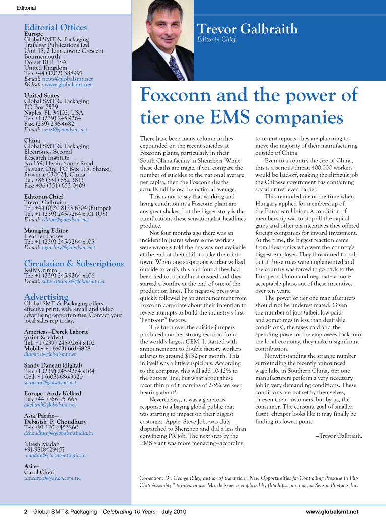
counterfeit exampleThis is a study conducted on Maxim part number MAX154XXXX. This component is characterized as an ADC single semi flash, 400KSPS 8-bit parallel, 24 pin SOIC component.
Visual inspection #1Using the IDEA-STD-1010 visual inspection standard, these components were subjected to the multipoint inspection process. It was immediately noticed that the top surface was very shiny and the texture was smooth. Additionally, the topography of factory fresh components has a small textured surface compared with the somewhat larger texture exhibited by these parts (Figure 1).
The suspicious top surface topography was compared to the bottom surface. The bottom surface displayed the typical small and grainy topography of a factory fresh component (Figure 2).
Visual inspection #2As noted above, the top surface had a very smooth and shiny surface. Each of the components in this lot were inspected and found to be equally shiny and smooth. A highly reflective surface on an electronic component is not normally what an inspector would expect to see under examination.
Visual inspection #3During the visual inspection, what appeared to be a false top coating that did not belong on this component was noted. The top and sides were observed under 40X power microscopy to confirm there was indeed a layer that did not come from the factory. In Figure 3, the false top coating is captured in the red highlighted box. The photo is taken from the side of the component looking over the top of the part.
Visual inspection #4The leads on this component were also given a thorough visual inspection under high-powered microcopy. There were no traces of alteration or counterfeiting
Keywords: Counterfeit Detection, IDEA-STD-1010
Much has been written about the curse of counterfeit electronic components having such a compounding effect on the security and economy of the United States.
This paper will demonstrate one of the techniques used by those responsible for polluting the open market inventories of the world with counterfeit components.
This sample of a counterfeit component and the photos shown are examples of a real inspection rejection event that successfully detected what could have been a tragic failure in an aerospace, military or mission critical system somewhere in the world.
It is the intent of this paper to share the knowledge and experience it took to detect this counterfeit component, with the hope that every organization may benefit from this information.
Art Ogg, World Micro, Roswell, Georgia, USA
False top coatings of a counterfeit component revealed layer by layer
Figure 1. Top surface of modified part. Figure 2. Bottom surface of modified part.

Global SMT & Packaging – Celebrating 10 Years – July 2010 – 11www.globalsmt.net
False top coatings of a counterfeit component revealed layer by layer
activity detected. This will be an important data point in the conclusion of this paper. See Figure 4 to observe that there are no issues of lead coplanarity, corrosion or retinning that may have been the result if subjected to a rework process.
Date code comparisonMaxim components will routinely have a component date code on both the top and the bottom surfaces. Not all manufacturers take this manufacturing step, but Maxim is one.
Notice in Figure 1, the last line has the date code of 9812. This tells the inspector the component was allegedly manufactured during the twelfth (12th) week of 1998.
However, notice the date code on the bottom of this component in Figure 2. The bottom line has a date code of 9609. Occasionally a certified inspector will see a variation between the two date codes on a Maxim part of one or maybe even two weeks. Any variance over two weeks is a variance that needs further explanation. This is a very big “red flag” to an inspector.
In this case, the markings tell us that the bottom section of this component was manufactured two years and three weeks prior to the top portion being attached. This is impossible and will never happen.
The overconfident counterfeiter has made the assumption that the inspector will not compare the top and bottom date codes and reject the lot based upon the lengthy variations in dates.
They will also assume that most facilities have no inspection procedure at all and the parts will be received and shipped without anyone taking a look for component flaws such as these.
resistance to solventsThe experienced professional inspector has learned that, in most cases, a mixture of three parts mineral spirits and one part alcohol will remove the ink from a counterfeited component. The reason this happens is the counterfeiter will seldom cure the ink like the original component manufacturer (OCM) does during their production runs.
The process where this solution is used to test the ink is known as the “Marker Permanency Test” and is documented in MIL-STD-883.
This solution and test procedure was administered to a sample of the components. The results were negative. This is another important data point to be discussed in the conclusion.
The experienced professional inspector has also learned that pure acetone will typically remove a false top coating placed on a component. An acetone wash was administered to the top surface of this component with negative results.
component measurementsThe experienced inspector has been trained to download the component’s datasheet from the Internet. This document has several very important tables, drawings and explanations about the component.
One of the more important data points contained in the datasheet is the measurements. In the case of this particular Maxim component, the thickness has a specification of between 1.73 mm and 1.99 mm. A random sample of five parts was taken from the lot and measured. The average thickness between these five parts was 2.36 mm. This resulted in +.63 mm above the shallowest
measurement of 1.73 mm (36%) and +.37 mm (19% out of specification) thicker than the high end of the thickness specification.
These components were far above the allowable thickness of acceptability. This will weigh heavily in the preliminary conclusions and how to proceed with proving these parts to be counterfeit.
preliminary conclusions Acceptable inspection findings1. The texture and topography of the
bottom surface is consistent with a factory fresh part.
2. The component leads remain untouched and are in pristine shape.
3. The components are not affected by the normal solvents used to validate if parts are indeed counterfeit.
Unacceptable findings1. The parts have an untypical shiny
reflective top surface.2. The top surface topography is not
consistent with a factory fresh component.
3. High power microscopy shows the addition of a false top coat on the top surface.
4. There is a two-year variance between the top surface date code and the bottom surface date code. This should never happen to a part coming from the factory.
5. The thickness specification has been exceeded by 19% above the high end of the thickness specification.
At this point, when the unacceptable findings of this inspection are weighed against the acceptable findings, there is more than enough evidence detected thus far to reject these components due to
Figure 4. Component leads pass inspection.Figure 3. False top known as blacktopping.

12 – Global SMT & Packaging – Celebrating 10 Years – July 2010 www.globalsmt.net
False top coatings of a counterfeit component revealed layer by layer
quality issues.The inspector has now applied most
of the thorough inspection protocols found in the IDEA-STD-1010 inspection standard. The parts could be rightfully rejected at this point.
In an attempt to learn more about the techniques being used by this counterfeiter, the decision was made to proceed further. The goal was to reconstruct the steps the
counterfeiter must have taken to produce the modified parts shown in this report
removal of the clear and shiny top coating The use of the solvents normally used to remove false top coats and uncured ink stampings resulted in failure. Apparently, the counterfeiter has used a process to prevent their use in testing parts for
uncured ink stampings.The second attempt to remove
the clear top coating also resulted in failure. A razor blade was used to scrape the coating from the top. This step caused more material to be removed than was desired. The decision was made to discontinue this procedure.
A piece of the clear coating that was removed from the top appears in Figure 5. The piece, shown in this photo, is estimated to be one-fifth the size of a period used in this report.
Under very high-powered
microscopy (300X), it was established that the thin clear top coating is actually just partially clear. The top layer of the false coating directly below the clear coat can be easily observed. Apparently, over time the clear epoxy coating has absorbed some quantity of the material used in the false top coat directly below it.
It has become dark in color as shown in Figure 5.
Small pieces of 3M 401Q Imperial™ Wetordry™ 2,000 grit sandpaper was applied to one side of the component as shown in Figure 6. ESD tape was applied to the left side of this component to protect it from the abrasive qualities of the sanding.
The right side was slowly abraded until the clear top coating was removed. The sanding process continued until the part markings were still visible on the right side, but all of the highly reflective material had been removed. All that remains in this photo on the right side depicts the beginning of the false top coat.
A calibrated caliper was used to measure the thickness of the component to the right of the red line. The thickness of the clear coating was determined to be .05 mm thick.
The component was further abraded to remove the entire thickness of the false top coat applied to this part. The same process and sandpaper used to remove the clear epoxy was also used to remove the false top coating.
Once the entire false top coating had been removed, the component thickness was once again measured with the calipers. The component was now back to its original thickness and measured 1.86 mm, placing it well within the 1.73 mm-1.99 mm specification.
Figure 7 shows the original component
Figure 5. Clear epoxy top coat material. Figure 6. Clear epoxy removed.
Figure 7. Original component surface.
Figure 8. Layers of counterfeiting rework.

Global SMT & Packaging – Celebrating 10 Years – July 2010 – 13www.globalsmt.net
False top coatings of a counterfeit component revealed layer by layer
surface the component would have had when it left the factory. At this point the part has had all of the material placed on it by the counterfeiters to conceal the true identity of the part.
important items to noticeFigure 7 shows the original top surface and markings as it came from the factory. Notice the original P/N was MAX154ACWG and the date code was 9609, shown on the bottom line.
Figure 1 shows this same part at the beginning of this investigation prior to any testing or chemical analysis being conducted. Notice the new P/N placed on the part by the counterfeiters is MAX154BEWG and the date code is 9812.
The original date code on the part is two years and three weeks older than the newer date code placed on the false top coat.
The original P/N has a suffix of “ACWG,” meaning it had an operating temperatureof(0˚Cto+70˚C).Thesecond P/N placed on the part has a suffix of “BEWG,” meaning it had an operating temperatureof(-40˚Cto+80˚C).
Figure 8 illustrates the layers of rework that were done on the counterfeit component.
Layer 1 is the original component measuring 1.86 mm thick with the original part number ink stamped showing MAX154ACWG.
Layer 2 shows the original part number and the original date code of 9609.
Layer 3 is a .45 mm thick false black topping placed on the top to hide the original P/N. It was made from a material that would not dissolve in acetone. This is very unusual since most false coatings will wash away using this solvent.
Layer 4 is the new part number of MAX154BEWG and a new date code of 9812.
Layer 5 is the clear coating of epoxy that is .04 mm thick. Epoxy is a material that is not affected by an acetone wash. It was placed there to prevent failure of the marker permanency test used by a certified inspector.
overall conclusionsThe workmanship on these parts is exceptional. The materials used, the clear epoxy top coating and the black topping placed over the original top surface were chosen to prevent detection by the usual marker permanency test and the use of acetone for testing false top coatings.
An inexperienced inspector may not have detected these reworked parts. The
visual attributes that gave them away were that the top surface topography did not match the bottom surface, the clear coating was shiny and reflective, and the date code on the top did not match the one on the bottom.
The ultimate proof, however, was the remarked part number that was for a part that can operate in a much wider temperature range, meaning it is more expensive, and that the original date of the part was two years younger than the remarked date code. By definition, this is a
reworked part.
Art Ogg, World Micro’s director of quality, is responsible for World Micro’s quality initiatives, product quality, ISO
certifications, technical documentation and quality team. Prior to joining World Micro, Mr.
Ogg held senior management positions with Seagate Technology and Digital Equipment
Corporation. He brings 40 years of high tech electronics experience to his position, and is
noted expert and regular speaker at industry trade events.
THEREARENOSHORTCUTSTOA5-MILDOTSmall, repeatable volumes area challenge. But not impossibleif you have been creating them aslong as we have. However, to doit well, you need three things:
Dispensing Expertisein a variety of applications:micro-attach, precision fill,highly-repeatable patterns;
Feasibility Testing andprocess verification based on yearsof product engineering, material flowtesting, and software control;
Product Development for patented valves,dispensing cartridges, needles, and accessories.
For Micro Dispensing, there is oneproduct line that is proven and trustedby manufacturers in semiconductorpackaging, electronics assembly,medical device, and electro-mechanicalassembly the world over.
R
www.dltechnology.comDL Technology is a registered trademark of DL Technology LLC. DispenseLink is a registered trademark of DL Technology LLC.HY-FLO is a trademark of DL Technology LLC.
DispenseLink® for MicroVolume Dispensing
Micro Valve
HY-FLO™ Valvewith Thermal Controls
DL Trade Ad 4_9:Layout 1 5/1/09 3:49 PM Page 1

14 – Global SMT & Packaging – Celebrating 10 Years – July 2010 www.globalsmt.net
Wafer-level solder sphere placement and its implications
introductionSolder bumping is often separated into several different categories: flip chip bumping (FC), wafer level chip scale packaging (WLCSP) and ball grid array (BGA). This categorization and affiliated nomenclature is partially based on the solder bump size and the type of equipment used to create the bump. Pushing the limits of each of the three traditional bumping technologies has allowed some overlap between these bumping classifications. But for the most part, volume manufacturing of flip chip, WLCSP, and BGA bumps are carried out using different processes steps on different types of equipment. Solder sphere placement is a technique that has been
shown to completely bridge this technology gap. The basic principle of this technology is to simultaneously pick up preformed solder spheres using a patterned vacuum plate and then accurately place them onto the bond pads of the wafer.
The solder sphere placement technique allows a single technology to be used for an array of different bumping applications. These include: • All wafer sizes from 100 to 300 mm
and fan-out substrates• All solder alloys (lead based, lead-free,
polymer core)• FC, WLCSP, and BGA bump sizes (60-
760 μm spheres)
This up-and-coming technology has been associated with several different names in the literature. These include: gang ball placement, solder ball transfer, wafer level solder sphere transfer, ultra solder ball bumping, and solder sphere placement.
The versatility of this technology can be further enhanced by coupling several other technologies into the solder sphere placement system. These include adding: 2D inspection capabilities, single sphere removal and replacement capabilities (repair and rework), and in-situ solder reflow (inert atmosphere hotplate).
The ultimate solder sphere placement system incorporates all of these discrete technologies into a single tool in order to increase versatility and assure high yields.
Keywords: Solder Bumping, Solder Sphere, Ball Placement, Sphere Transfer, Flip Chip, WLCSP
There are three main packaging technologies used by the semiconductor industry today to create solder bumps on wafers: paste printing, electroplating, or sphere dropping1. The choice between these technologies is highly influenced by the following criteria: the bump size & pitch requirements, cost and overall yield. As the bumping industry evolves, many of the deficiencies and trade-offs associated with the three bumping technologies are no longer acceptable. As a consequence, a significant transition is occurring toward a fourth bumping alternative: solder sphere placement2. This technique offers wide flexibility in bump size (40-760 µm), very high bump yields (>>99%) and low cost (sphere price dominated).
Andrew Strandjord, Thomas Oppert, Thorsten Teutsch, and Ghassem Azdasht, PacTech—Packaging Technologies, Inc., Nauen, Germany
Wafer-level solder sphere placement and its implications
Figure 1. Ultra-SB2™ solder sphere placement tool.
Figure 2. Solder sphere reservoir filled with solder spheres.

Global SMT & Packaging – Celebrating 10 Years – July 2010 – 15www.globalsmt.net
Wafer-level solder sphere placement and its implications
The final configuration of the tool is often dictated by the product distribution (flip chip vs WLCSP vs BGA volumes).
Wafers or substrates for WLCSP and BGA applications have relatively large solder bumps and have relatively few interconnects compared to flip chip applications. These larger spheres are placed in extremely high yields by the solder sphere placement tool and the
added expense of incorporating inspection and rework capabilities might not be justified. High I/O flip chip applications, on the other hand, often require very high bump yields in order to achieve high die yields. In these applications, integration of all the options makes good economical and throughput sense.
The recent availability of highly uniform solder spheres at lower costs has
allowed the technique of solder sphere placement to expand within the industry. Typical lead-free spheres (SAC alloys) range in price between $25-50 per million when purchased in volume. As the volume of sphere consumption continues to increase, the cost will continue to come down. Spheres of other alloys, including polymer core and copper core spheres, are also starting to become more prevalent within the industry as alternatives to SAC alloys.
process flowA predetermined number of spheres are automatically dispensed into a sphere reservoir (Figure 2). The amount of spheres in this reservoir is important in order to achieve high transfer yields. This value is approximately 20-30% more than the number of I/O on the wafer.
The fixture which picks up the spheres consists of two main components: a vacuum head which is mounted to a high precision x-y-z translation stage and a tooling plate which contains small holes that is mechanically mounted to the vacuum head (Figure 3).
The tooling plate is patterned with openings that correspond directly with the locations of the I/O pads on the wafer. This tooling is created using similar methods to that of making a nickel-plated surface-mount stencil. There are a large number of vendors who can now manufacture these stencils using electroforming techniques. The size of openings in the tooling plate is designed to be slightly smaller than the size of spheres that will be placed onto the wafer.
The sphere placement head is then lowered onto the sphere reservoir and the vacuum is applied to the vacuum port (Figure 4). The vacuum alone is not sufficient to efficiently transport and relocate the solder spheres into each opening in the stencil template. The application of ultrasonics is applied to the reservoir to aid in sphere movement.
Optimization of the ultrasonic amplitude and frequency, in addition to the vacuum, is required for each spheres size and I/O density in order to maximize sphere relocation to the template. Even with this optimization, an unwanted sphere can occasionally adhere to the stencil. This is commonly a result of static electricity. Removal of these extra spheres is accomplished passing the head over a deionizing air knife (Figure 5).
The placement head is then moved over to the transfer station within the tool. A prefluxed wafer has been pre-positioned from a wafer cassette onto the
Figure 3. Sphere placement head positioned over the solder sphere reservoir.
Figure 4. Sphere placement head lowered onto sphere reservoir. Vacuum and ultrasonics applied to reservoir.
Figure 5. Shear placement head with solder spheres passing over deionizing air knife to remove any excess spheres.
Figure 6. A pre-fluxed wafer is automatically placed onto the vacuum wafer chuck.

16 – Global SMT & Packaging – Celebrating 10 Years – July 2010 www.globalsmt.net
Wafer-level solder sphere placement and its implications
vacuum chuck at this station (Figure 6). The application of tacky flux is applied in a separate tool prior to being loaded into the sphere placement tool. For WLCSP and BGA applications, screen-printing or stencil printing are used to apply this flux.
For flip chip applications, spin coating is used to apply the flux. The important criteria for all applications include flux thickness and viscosity.
The solder transfer head is then moved over the wafer chuck and a bidirectional
optical sensor is extended in between the head and the chuck (Figure 7). This inspection system allows the spheres within the apertures of the stencil template to be aligned to the bond pads on the wafer. In addition to alignment, this sensor performs a 2D scan of the stencil template to confirm that all apertures contain a solder sphere and also inspects for unwanted stray spheres that may still be attached to the template. The tool software can then make a decision based on user criteria to continue to the transfer step, return further cleaning at the air knife station, or go completely back to the sphere pickup station to fill in empty apertures with spheres.
The solder placement head is then lowered toward the wafer until the solder spheres penetrate the flux and touch the wafer bond pads (Figure 8). The mechanical downward force is adjusted to help drive the spheres onto the pads. The vacuum is then released and a N2 back pressure is applied to the placement head to assist in releasing the spheres.
The head is then raised and the optical inspection sensor is reinserted over the wafer, and the wafer is scanned to quantify transfer yields (Figure 9). This scan will document the x-y coordinates of any missing or misplaced spheres that may have moved after the transfer process.
For flip chip applications, where high bump yields are an absolute requirement to give high die yields, integration of rework/repair capabilities is critical. It is common for high-end applications, such as microprocessors, to have hundreds of interconnects per die. Even small bump yield losses can translate into high die yield losses.
A repair head, which is based on the SB2 ™ sphere bumping process3, is used to repair any defects identified in the 2D inspection (Figure 10). For missing bumps, a sphere is dropped onto the pad where the bump is missing. This process has no mechanical contact with the wafer and solder bumps are deposited at a rate of 6-10 spheres per second. For misplaced or damaged spheres, the capillary head of the SB2 tool is lowered over the sphere, the capillary heated, and a vacuum is applied to the tube, which removes the sphere. In both cases a laser pulse can be added to help liquify the flux or melt the solder sphere.
The wafer is then ready for final reflow. For most WLCSP and BGA devices the wafers are placed back into the wafer cassette. Once all 25 wafers are bumped, the cassette is moved over to a linear
Figure 7. Optical sensor extended between the wafer and placement head. Aligning the template to the wafer and also inspecting for missing or unwanted spheres.
Figure 8. Tooling head lowered on wafer to bring spheres into contact with the fluxed wafer pads.
Figure 9. Raise placement head and insert optical sensor over wafer.
Figure 10. SB2 repair head positioned over a pad with a missing solder bump.

SEMICON West#911

18 – Global SMT & Packaging – Celebrating 10 Years – July 2010 www.globalsmt.net
Wafer-level solder sphere placement and its implications
conduction oven for reflow. Alternatively the wafers can be moved over to a reflow chamber located within in the tool (Figure 11). This is more common for fine pitch flip chip devices.
After reflow, the wafers are placed back into the process cassette and cleaned in a batch process using a combination of ultrasonics, solvents and water rinsing (Figure 12).
conclusionsThe wafer level solder sphere placement tool can perform flip chip, WLCSP, and BGA bumping operations (Figure 13). The configuration of the tool is dictated by the product distribution (Tables 1 and 2). Defects in the ppm range result in die yields greater than 99%. Wafer throughputs are between 20-45 wafers per hour.
acknowledgementsThe authors would like to thank all the engineers and technicians of PacTech for their help in developing the solder sphere placement technology.
references1. D. S. Patterson, P. Elenius, and J.
Leal, “Wafer Bumping Technologies – A comparative analysis of Solder Deposition Processes and Assembly Considerations”, EEP Vol. 19-1, Advances in Electronic Packaging, Hawaii, 1997, pp. 337-351. M. Whitmore, M. Staddon, D. Manessis: “Development of a Low Cost Wafer-Level Bumping Technique”, International Wafer-Level Packaging Conference, 2004. J. Ling, T. Strothmann, D. Stepniak, P. Elanius, “Flex-On-Cap Solder Bump for 300mm Wafer”, Semicon, Singapore, 2001. T. Flynn, C.W. Argento, and J.Obrien, “Electro-plated flip chip Wafer Bumping Interconnect Technology Solutions for the 21st Century”, Proceedings of International Symposium on Microelectronics, Chicago, Illinois, October 26-28, 1999, pp. 8-12.
2. K. Tatsumi, K. Shimokawa, E. Hashino, Y. Ohzeki, T. Nakamori, and M.Tanaka, “Micro-Ball Bumping Technology for flip chip”, The International Journal of Microcircuits and Electronic Packaging, Volume
22, Number 2, Second Quarter 1999 (ISSN 1063-1674), pp.127-136. Andrew Strandjord, Thorsten Teutsch, Axel Scheffler, Thomas Oppert, Ghassem Azdasht, and Elke Zakel, “WLCSP Production Using Electroless Ni/Au Plating and Wafer Level Solder Sphere Transfer Technology”, IWLPC, San Jose, CA, October 14th, 2008.
Andrew Strandjord “Solder Ball Transfer for flip chip and WLCSP”, Advanced Packaging, March 19, 2008.
3. P. Kasulke, W. Schmidt, L. Titerle, H. Bohnaker, T. Oppert, E. Zakel, “Solder Ball Bumper SB2-A flexible manufacturing tool for 3-dimensional sensor and microsystem packages”, Proceedings of the International
Figure 11. Solder bumps reflowed on heated vacuum chuck.
Figure 12. Bumped, reflowed and cleaned wafer.
Figure 13. SEM image of 60 µm flip chip bumps and 300 µm WLCSP solder bumps.
Process Step Equipment
1. Flux deposition Stencil or screen printer
2. Sphere transfer Basic solder sphere placement
3. Reflow Linear oven
4. Wafer clean Solvent and/or DI water tools
5. Inspection 2D scanner
Table 1. Process steps for WLCSP and BGA ap-plications.
Process Step Equipment
1. Fluxing Spin coating
2a. Sphere transfer
Integrated solder sphere placement tool b. 2D inspection
c. Rework
d. Hot plate reflow
3. Wafer clean Solvent and/or DI water
Table 2. Process steps for flip chip applications.
continued on page 25

Global SMT & Packaging – Celebrating 10 Years – July 2010 – 19www.globalsmt.net
Addressing package advancement challenges with innovative contactor probe technology
SEMICON West#6356

20 – Global SMT & Packaging – Celebrating 10 Years – July 2010 www.globalsmt.net
Integrated testing, modeling and failure analysis of CSPnl for board level reliability
Using global semiconductor shipments as a measure of world electronic manufacturing activity, Chart 1 shows the magnitude and timing of our most recent global recession (& recovery) relative to the “Internet Bubble” crash of 2001/2002. Recovery was much quicker in 2010, thanks to dramatically better inventory control. Ten years ago, large finished goods and electronic component stocks had to be consumed (or written off) before new purchases could resume. That is not the case today. Chart 2 is a companion to Chart 1, showing 3-month growth (rather than actual US$) of monthly world semiconductor shipments. 3/12 chip growth recently peaked (at a whopping +58%) in March. The early-2010 massive chip shipment growth rates were of course calculated relative to the deep trough of early 2009. As we look to the second half of this year, growth will slow (chip shipments will still be increasing but at a more moderate pace). 2010 should still end with almost a
30% semiconductor expansion compared to last year.
From Chart 1 note that world April 2010 chip shipments exceeded their pre-crash high of 2008. The global electronics industry has quickly recovered (to pre-crash levels)!
Global electronic equipment shipment growth (Chart 3) is now in positive territory (3/12 > 1.0) in all regions. Converted to monthly US dollars (Chart 4), the vast majority of the present electronic equipment production expansion is in SE Asia—but all regions are improving.
Looking forward, semiconductor shipments (Chart 5) are projected to jump 28.6% in 2010 followed by an added 5.6% in 2011, with further growth until at least 2012. Semiconductor capital spending (Chart 6) is forecasted to increase 83.5% this year and then an additional 13.9% in 2011. Spending for capital equipment (Chart 7) remains highly volatile! Feast or famine is the rule!
World printed circuit shipments
are also strong (Chart 8) with SE Asia dominating global production. On a consolidated (world) basis PCB shipments dropped about 20% in 2009 but now appear to be on track for 28% growth this year (up from Custer Consulting Group’s +20% growth estimate made in early 2010). Most supply chain prognosticators have recently revised their 2010 forecasts upwards due to stronger than expected demand.
The global recovery is certainly well underway as we move into the normal late summer/early autumn “busy season.”
end markets• Worldwide IT spending will increase by
3.8% this year at constant currency, to $1.47 trillion; hardware to grow 6.4% at constant currency; IT market will increase by 13.7% in China, and by 13.8% in India.—IDC
• Digital information grew 62%y/y in 2009 to 800 billion gigabytes (0.8 Zettabytes).—EMC
Walt Custer and Jon Custer-Topai
Strong global growth throughout supply chain
Chart 1. Chart 2.
World Semiconductor Shipments Monthly US$
SIA
1 1 1 1 1 1 1 1 1 1 1 1 1 1 1 1 1 1 1 1 1 1 1 1 1 1 1 183 84 85 86 87 88 89 90 91 92 93 94 95 96 97 98 99 00 01 02 03 04 05 06 07 08 09 10
0
5
10
15
20
25US$ Billions (3-month average)
20100604
2009 recession much sharper but shorter than 2001
Global Semiconductor Shipments3-Month Growth Rates on $ Basis
Total $ Shipments from All Countries to an AreaSIA website: www.sia-online.org/
15915915915915915915915915915915915915915915915915915915915915915915915915915915/1084 85 86 87 88 89 90 91 92 93 94 95 96 97 98 99 00 01 02 03 04 05 06 07 08 09 10
0.4
0.6
0.8
1
1.2
1.4
1.63/12 Rate of Change
1
2 3
4
5
6
7
8
9
10
20100604
11 12
13
Strong global growth throughout supply chain

Global SMT & Packaging – Celebrating 10 Years – July 2010 – 21www.globalsmt.net
Strong global growth throughout supply chain
• Chinese electronics manufacturing export delivery value increased 24.4% y/y and 5.7% m/m to CNY 267.8 billion in April 2010.—MIIT
• Global smart homes market will grow at a 16.5% CAGR from 2009 to 2014 to $13.4 billion by 2014.
Computers & peripherals• Worldwide mobile PC shipments grew
43.4% y/y to 49.4 million units in 1Q10.—Gartner
• Global PC shipments will rise 22% to 376.6 million units in 2010 plus an additional 10 million media tablets.—Gartner
• Notebook sales rose 21% to $36.1 billion in 1Q’10. —Gartner
• Worldwide media tablets shipments will reach 7.6 million in 2010.—IDC
• Netbook shipments are expected to grow from 36.3 million in 2009 to 58 million in 2010.—ABI Research
• Stereo 3-D PC market shipments will rise from rising from nearly one million to 75 million by 2014.—Jon
Peddie Research• Worldwide server market revenue is
expected to increase 4.6% y/y to $10.4 billion in 1Q10.—IDC
• HDD industry will deliver more than 300,000 petabytes of storage capacity over the next five years to enterprise datacenters and clouds.—IDC
• Worldwide hardcopy peripheral shipments grew 9.1% y/y to 28.7 million units in 1Q10.—IDC
Mobile communications• Worldwide mobile phone sales to end
users grew 17% to 314.7 million units in 1Q10.—Gartner
• Worldwide converged mobile device (smartphone) market grew 56.7% y/y to 54.7 million units in 1Q10.—IDC
• Handset navigation shipments will rise from 30 million units in 2010 to 181 million units in 2015.—ABI Research Forecast
• Touch screen shipments expanded 29% y/y to 606 million units in 2009.—DisplaySearch
• China added 8.497 million phone users in April 2010 reaching a total of 786.5 million.—MIIT
Consumer electronics• U.S. household spent $1,380 (on
an average) on consumer electronics products in the past 12 months, an increase of $151 from last year.—CEA
• Global 3D TV shipments are expected to grow from 4.2 million units in 2010 to 12.9 million units in 2011, 27.4 million units in 2012 and 78.1 million units in 2015.—iSuppli
• U.S. videogame hardware, software and accessories sales fell to $766.2 million in April from $1.03 billion a year earlier.—NPD Group
Automotive electronic systems are expected to rise from $125 billion in 2009 to $244 billion by 2017.—Strategy AnalyticsGlobal commercial navigation system shipments will grow from 3 million units in 2010 to 7.5 million units in 2015.—ABI Research
Global Electronic Equipment Shipment Growth
1 4 7 10 1 4 7 10 1 4 7 10 1 4 7 10 1 4 7 10 1 4 7 10 1 4 7 10 1 4 7 10 1 4 7 10 1 4 7 10 1 400 01 02 03 04 05 06 07 08 09 10
CALENDAR YEAR
0.6
0.7
0.8
0.9
1
1.1
1.2
1.3
1.4
1.5
1.63/12 rate of growth in local currency
Taiwan/ChinaEuropeJapanUSA0
20100620
Europe = Eurostat EU27 NACE C26 (computer, electronic & optical products)
World Electronic Equipment Monthly Shipments
Converted @ Constant 2008 Exchange Rates
1 3 5 7 9111 3 5 7 9111 3 5 7 9111 3 5 7 9111 3 5 7 9111 3 5 7 9111 3 5 7 9111 3 5 7 9111 3 5 7 9111 3 5 7 9111 3 500 01 02 03 04 05 06 07 08 09 10
CALENDAR YEAR
0
20
40
60
80
100$ Billions
N America Europe Japan SE Asia
Source: Custer Consulting Group
20100620
Chart 3. Chart 4.
149.4
204.4
138.9 140.8166.3
213.1227.4
247.7 255.6 248.6226.3
291.0307.4
320.0
1999 2000 2001 2002 2003 2004 2005 2006 2007 2008 2009 2010 2011 20120.0
50.0
100.0
150.0
200.0
250.0
300.0
350.0
N. America 47.5 64.1 35.8 31.3 32.3 39.1 40.7 44.9 42.3 37.9 38.5 48.1 50.4 52.1Europe 31.9 42.3 30.2 27.8 32.3 39.4 39.1 39.9 41.0 38.2 29.9 38.2 40.1 41.6Japan 32.8 46.7 33.1 30.5 38.9 45.8 44.1 46.4 48.8 48.5 38.3 44.8 47.3 49.2
Asia Pacific 37.2 51.3 39.8 51.2 62.8 88.8 103.5 116.5 123.5 124.0 119.6 159.9 169.6 177.1
WSTS 6/2010
Worldwide Semiconductor Market by GeographyWSTS Forecast
20100622
-9%
+5.6%+28.6%
60.063.4
44.0
25.9
47.554.1
58.351.7 49.4
2006 2007 2008 2009 2010 2011 2012 2013 20140.0
10.0
20.0
30.0
40.0
50.0
60.0
70.0$ Billions
Wafer Fab Equip 32.5 36.0 24.2 12.7 27.2 29.1 33.0 29.3 28.4Packaging & Assembly Equip 5.4 5.2 4.0 2.7 5.5 5.6 5.0 3.4 3.9
Automated Test Equip 4.1 3.6 2.4 1.1 2.7 3.0 2.8 2.1 2.3Other Capital Spending 17.9 18.7 13.3 9.3 12.1 16.3 17.5 16.9 14.8
Gartner 6/2010
Worldwide Semiconductor Capital Spending20100622
-41%
+83.5%
+13.9%
Chart 5. Chart 6.

22 – Global SMT & Packaging – Celebrating 10 Years – July 2010 www.globalsmt.net
Strong global growth throughout supply chain
eMs, oDM & related assembly• EMS industry had 11 merger &
acquisitions in 1Q10.—Lincoln International
• Solar contract manufacturing is expected to grow from 1,100 MW in 2010 to 4.1 GW in 2014.—iSuppli
Ability Enterprise set up production base in eastern China for cameras, video recorders, optical lenses, digital photo frames, LCD monitors and projectors.Adeptron received a US$ 1.3 million EMS contract from a defense OEM customer and a $1.5 million assembly order for smart grid applications.Aero Stanrew obtained BE EN 9100:2003 and ISO 9001:2008 certifications.Assel added a NORDSON Asymtek SL-940 conformal coating system and a TC-2600 V4 IR oven.Assembly Contracts entered a contract manufacturing partnership with Cinterion.Bogart invested in a MYDATA P&P SMT line with jet printer MY500 and vapor-phase reflow soldering system.Celestica: • received a manufacturing order
for LumiSmart devices from Cavet Technologies.
• received an outsourcing agreement from HP Ireland that included the transfer of 140 workers.
China Wireless Technologies will open a handset assembly plant in India by 2012.Compal earned US$0.064 EPS in 1Q10, becoming world‘s most profitable NB contract manufacturer. CSM added an Asymtek Century C-740
automated, conformal coating application system.Diversified Systems ended operations.Elcoteq: • Bangalore received Excellent Award
from Quality Circle Forum of India.• becomes Sharp’s partner for the KIN
Windows phones.• elected Jorma Vanhanen chairman and
Heikki Horstia deputy chairman.• sold ZAO Elcoteq (St Petersburg,
Russia) operation to Optogan CJSC.
Electronqiue Lacroix Tunisia obtained EN9100 certification.Elprog added an Assembléon pick & place machine and screen printer.EPE moved to larger facility to accommodate 150% growth over past three years.EPIC Technologies received Volkswagen Group Award, 2010.Etek Europe launched used SMT division.Flextronics: • celebrated production of 25,000
Redbox DVD rental kiosks in Creedmoor, North Carolina.
• expanded Citrix Systems’ partnership to include joint design of new hardware products.
• was named ‘Strategic Partner of the Year’ and ‘Best-in-Class’ supplier by LSI.
• expanded notebook PC capacity in China to 15 million units/ yr.
• received solar panel manufacturing contract from SunPower.
• added 1,500 workers at its NB PC production in Taiwan.
Foxconn /Hon Hai:• installed safety nets and asked workers
to sign ‘no suicide’ agreement at its Shenzhen, China plant.
• employees were arrested for stealing $60,000 in processors at the Santa Teresa plant in Mexico.
• received Dell enterprise notebook orders for 2011.
• plans to ship 24 million 4G iPhones in 2010.
Frontline India added a DEK Horizon 03iX platform.
5.4
10.1
11.7
13.012.9
11.3
6.6
5.6
4.1 4.14.7
5.75.1
5.6
4.44.9
9.8 9.48.7 8.8
9.4
7.6 8.0 8.0
9.6 9.6
11.010.3
10.811.011.2
9.810.6
7.8
6.6
4.6
3.12.7
4.5
5.7
7.5
1 2 3 4 1 2 3 4 1 2 3 4 1 2 3 4 1 2 3 4 1 2 3 4 1 2 3 4 1 2 3 4 1 2 3 4 1 2 3 4 100 01 02 03 04 05 06 07 08 09 10
0.0
2.0
4.0
6.0
8.0
10.0
12.0
14.0
16.0$ Billions
Europe 1.4 1.5 1.7 1.9 1.6 1.0 0.7 0.6 0.4 0.5 0.5 0.6 0.5 0.7 0.8 0.9 0.9 0.9 0.9 0.8 0.7 0.9 0.9 0.9 0.9 0.9 0.8 0.6 0.8 0.7 0.7 0.5 0.6 0.6 0.4 0.2 0.2 0.3 0.3Japan 2.2 1.8 2.6 2.6 3.4 1.8 1.5 1.0 0.9 0.8 1.1 1.0 1.3 1.5 2.2 2.0 2.1 2.0 2.1 1.6 2.5 2.0 2.3 1.9 2.7 2.3 2.3 2.1 2.6 2.4 2.4 1.9 1.7 1.1 0.8 0.3 0.5 0.6 0.9
N America 2.4 3.2 3.5 3.9 3.0 2.2 1.7 1.4 1.5 1.3 1.6 1.6 1.4 1.1 1.2 1.4 1.4 1.7 1.6 1.4 1.4 1.3 1.8 1.8 1.8 1.9 1.8 1.5 1.7 1.6 1.8 1.3 1.1 1.4 1.1 0.7 0.7 0.9 0.9Korea 0.8 1.2 0.9 0.9 1.0 0.5 0.3 0.4 0.3 0.4 0.5 0.6 1.1 1.0 1.5 1.1 1.2 0.9 2.3 1.2 1.0 1.3 1.8 1.5 2.0 1.8 2.5 1.8 1.6 1.6 1.7 1.4 1.2 0.5 0.3 0.4 0.8 1.1 1.9
Taiwan 2.3 2.5 2.5 2.0 1.1 1.0 0.7 0.4 0.5 1.1 1.1 0.8 0.5 1.2 2.0 1.7 1.9 2.2 1.4 1.6 1.3 1.4 1.6 1.8 1.9 2.1 2.0 3.2 3.2 2.3 2.4 1.5 0.8 0.4 0.3 0.7 1.4 2.0 2.2China 1.9 0.9 0.5 0.4 0.3 0.2 0.4 0.4 0.4 0.6 0.9 0.5 0.7 1.2 0.5 0.5 0.8 0.5 0.4 0.2 0.1 0.1 0.4 0.3 0.4ROW 1.1 1.5 1.7 1.6 1.2 0.3 0.8 0.4 0.4 0.7 0.9 0.5 0.8 4.4 4.9 0.3 1.5 0.7 0.7 0.7 0.7 0.7 0.7 0.8 1.0 1.0 0.9 0.8 0.6 0.8 0.8 0.7 0.8 0.8 0.4 0.1 0.2 0.5 0.6 0.8
www.semi.org, 6/2010
Semiconductor Capital Equipment Shipmentsby Area
20100622
Chart 7.
World PCB Monthly ShipmentsConverted @ Constant 2008 Exchange Rates
13 5 7 91113 5 7 91113 5 7 91113 5 7 91113 5 7 91113 5 7 91113 5 7 91113 5 7 91113 5 7 91113 5 7 91113 5 7 91113 599 00 01 02 03 04 05 06 07 08 09 10
CALENDAR YEAR
0
500
1000
1500
2000
2500
3000
3500N America Europe Japan SE Asia
Source: Custer Consulting Group
20100620
Chart 8.

SurfaceMountTechnology
CREATINGVALUECREATINGVALUECREATING
automotiveconsumerautomotiveconsumerautomotivecomputerconsumercomputerconsumer
telecomcomputertelecomcomputer
www.vitechnology.com
SurfaceMountTechnology
consumercomputerconsumercomputerconsumertelecomcomputertelecomcomputer
AOI solutions to reduce defective PCBAs
3DSPI
by S
ynap
se 7KDL
SERIES
Large board Dual-lane 5KSERIES
Innovative Fast and Compact
computertelecomcomputertelecomcomputer

24 – Global SMT & Packaging – Celebrating 10 Years – July 2010 www.globalsmt.net
Strong global growth throughout supply chain
Hanza Intressenter acquired all outstanding shares of Hanza from HSF Group.Incap received a rotor component manufacturing supply contract from ABB Oy, Machines.Interphase Engineering expanded its design & contract manufacturing services.Itron added 40 new jobs and $4 million in new equipment.Jabil implemented carbon footprint, on-demand program throughout entire organization.JJS Electronics:• appointed Richard Barratt principal
NPI engineer.• developed training process which
promotes step-by-step analysis supported by pictorial guidance.
Kimball Electronics received a manufacturing contract for Third Eye retroscopes from Avantis Medical Systems.King Jim began offering EMS services in Malaysia.Kitron received a NOK 45 million/year contract for electronics manufacturing and assembly of industrial tools from Atlas Copco Tools.LaBarge: • received ANSI/ESD S20.20
certification at its Appleton (WI), Pittsburgh (PA) and Tulsa (OK) manufacturing facilities.
• received a $1.5 million electronic assemblies contract from Northrop Grumman for F-16 fighter fire control radar system.
Macrotron Systems moved to 75,000 SF
manufacturing plant in Fremont, CA.Nortech Systems acquired Trivirix.PartnerTech added six Trumpf machines at its new Myslowice, Poland, plant.Plexus: • received a solar inverter EMS contract
from Sustainable Energy Partners.• invested in a 1,800 SF Renewable
Energy Lab.Proxy Electronics (Sweden) filed for bankruptcy protection.Sanmina-SCI Israel Medical Systems is spending $10 million to build a plant in Suzhou, China.Season Group expanded into the U.S. with the acquisition of DC Electronics and its San Antonio facility.SinoHub commenced operations at its new 77,500 SF mobile phone manufacturing facility in Shenzhen, China.SMTC began providing Kontron with PCB and module level assembly manufacturing in Chihuahua, Mexico, and Dongguan, China.Sparton received a $830,000 manufacturing contract for SP3004D digital compass for military warfare equipment.Spectrum Control received $13.1m multiyear contract for complex microwave assembly.Stadium Electronics appointed Peter O’Keeffe business improvement manager.Suntron consolidated its Manchester, NH, and Lawrence, MA, operations into a larger facility in Methuen, MA.Surface Mount Technology: • completed renovation of SMT
Engineering, LLC.• will add 25,000 additional SF of
manufacturing space by 4Q’10.Televés S.A. invested in a SMT production line consisting of Siplace SX2 and Siplace CA (chip assembly) machines.Vega Grieshaber KG (Schiltach, Germany) implemented Siplace Facts for its SMT production inventory management system.Victron: • opened Victron de Mexico.• passed UL DQS’ tri-annual audit
of ISO14001:2004 Environmental Management System, and ISO9001:2008 and ISO13485:2003 quality systems.
Videoton Electronics Assembly Services received a EMS manufacturing contract from Linak for furniture electronics.Xenterio appointed Ernst Gockel sales & marketing manager.
Materials & process equipmentIndustrial automation electronics equipment (excluding software and services) revenue declined 14.3% y/y to $74.9 billion in 2009.—IMS ResearchAzuma renewed its PCB copper plating lines.3M: • Electronic Solutions Division
introduced a halogen-free embedded capacitance material.
• released its material library for ANSYS simulation software.
Agilent Technologies acquired Varian.AIM appointed Andy Dolan business development manager.Arlon and Rogers Corporation resolved their patent infringement litigation.BASF will expand its annual methanesulfonic acid capacity in Ludwigshafen, Germany, to 30,000 tons.Chemtura opened a Technical Center of Excellence in Nanjing, China for the Asia-Pacific region.ChipChecker launched electrical inspection services.Co-Tech • is developing copper foils for electric
car batteries.• will ship 15,000 tons of copper foil in
2010. CyberOptics named Daniel Good VP of corporate development and Tim Skunes VP of technology and business development.DEK expanded its presence in South America in partnership with Fuji Do Brasil.DKN Research began supplying substrates for printable electronics engineering trials.Dow Electronic Materials: • opened a new research and
World PCB Shipments (with forecast)Converted @ Constant 2008 Exchange Rates
1357 9111 357 91113 57911135 79111357 9111 35791113 57911135 79111357 9111 35791113 57911135 7911199 00 01 02 03 04 05 06 07 08 09 10 11
CALENDAR YEAR
20
30
40
50
60$ Billion
Source: Custer Consulting Group - synthesized from Henderson Ventures annual estimates and N. American, Japanese & Taiwan/China monthly PCB shipments and SIA European chip shipments
20100620
51.742.937.631.729.4
Assumptions:Europe = composite European SIA & local PCB assoc dataJapan & N. America from JPCA & IPC dataTaiwan/China based upon 44 rigid & flex company compositeRest of Asia growth = Taiwan/China 44 company compositeData scaled to match Henderson Ventures annual totals2007 based upon sum of monthly totals
38.6 31.231.6 54.3 51.1 40.9 52.6
-20%
+28%
Chart 9.

Global SMT & Packaging – Celebrating 10 Years – July 2010 – 25www.globalsmt.net
Strong global growth throughout supply chain
• development center in Seoul, Korea.• received Excellent Supplier award from
HannStar Board.Dow Europe raised epoxy products prices in Europe.Electro Scientific Industries received Provectus Award for advanced IP processes.EMC will ramp up CCL capacity at each of its plants in Taiwan and China in 4Q.Europlacer opened 3,000 SF facility in Tampa, Florida.Fabrico and Henkel entered a partnership for Loctite bonding, joining & sealing solutions.Furukawa Electric will expand capacity for general grade copper foil for rigid PCBs to 1,200 tons/ month with construction of 2nd factory in Taiwan which is scheduled for operation at end of fiscal 2014.GCT started production at its diamond coating facility in Weingarten, Germany.GOEPEL electronic and InterElectronic Hungary entered a partnership to distribute AOI systems for electronic assemblies in Hungary and Romania.Isola received OHSAS 18001:2007 and DIN EN ISO 14001:2004 3-year recertification from TÜV Rheinland (Technical Inspection Authority).Kester appointed Michael Fullbrecht European sales manager.Laird released a low-cost high-performance thermal substrate for LED module applications.Mallinckrodt Baker: • named former Rohm & Haas CEO
Raj Gupta chairman. • is expanding its solar panel and flat-
screen TV businesses.Manncorp introduced two “High-Throughput Flex Lines” turnkey SMT lines, which include twin MC-385 pick and place machines and “Box Builder Line” with MC-387 placer.Nissan Chemical developed a organic-inorganic hybrid polymer for optical printed circuit boards.Park Electrochemical:• elected Emily Groehl to its board of
directors.• appointed Dr. Ke Wang director of
research & development and W. Douglas Leys director of advanced material applications.
• introduced E-710 Easycure low temperature cure epoxy prepreg.
Seica named Zero Defects International its North American sales agent for bare board flying probes.Siemens Electronics Assembly Systems (SEAS) introduced capacity-on-demand business models: SIPLACE Peak Demand and SIPLACE Floating Demand.Sun Chemical named Toryon
Technologies its national distributor for circuit product materials.Taiflex PV’s back sheet factory in China began production in July.Tamura started volume production of a flexible black light absorber for flexible circuits designed as LED module substrates.Taiwan Glass Industrial plans to raise glass fabric capacity by 20,000 tons in 2H’11.Ticona acquired Dupont LCP and PCT product lines.T-Tech introduced its Quick Circuit QCJ5 advanced prototyping system.TUC expanded its CCL front-end processing capacity to 300,000 units/ month.Unimicron began offering Shocking Technologies’ XStatic™ voltage switchable dielectric material to its customers.Vi TECHNOLOGY appointed Koen Gutscoven worldwide VP of sales.Viking:• formed an equipment supply and
service division for the electronics production industry.
• Test named Peter Collins sales manager
Walt Custer is an independent consultant who monitors and offers a daily news service
and market reports on the PCB and assembly automation and semiconductor industries. He
can be contacted at [email protected] or visit www.custerconsulting.com.
Jon Custer-Topai is vice president of Custer Consulting Group and responsible for the
corporation’s market research and news analysis activities. Jon is a member of the IPC and active in the Technology Marketing Research Council.
He can be contacted at [email protected].
1. Electronics Manufacturing Technology Symposium (22nd IEMT), Berlin, April 27-29, 1998. Elke Zakel, Lars Titerle, Thomas Oppert, Ronald G. Blankenhorn, “High Speed Laser Solder Jetting Technology for Optoelectronics and MEMS Packaging”, Proceedings of the International Conference on Electronics Packaging (Tokyo, Japan), Apr. 17-19, 2002.
Andrew Strandjord is senior manager of advanced packaging at PacTech USA. He
received his Ph.D. in organic chemistry from the University of Minnesota.
Mr. Oppert is vice president global sales & marketing at PacTech in Nauen, Germany. He
earned a master’s degree in electrical engineering from the Technical University of Berlin
in 1995. Thomas Oppert has co-authored more than 50 technical papers related to
semiconductor packaging. [email protected]
Dr. Thorsten Teutsch is president of PacTech-USA. He received his Ph.D. in physical chemistry and surface science from Fritz-Haber
Institute of the Max Planck Society. [email protected]
Mr. Ghassem Azdasht is co-founder and CTO of PacTech GmbH. He studied
mechanical engineering and laser technologies at the Technical University Berlin. Mr. Azdasht
has authored of over 100 publications and patents related to wire bonding, flip chip, and
laser assembly. [email protected]
Wafer-level solder sphere placement and its implications— continued from page 18

26 – Global SMT & Packaging – Celebrating 10 Years – July 2010 www.globalsmt.net
Steps toward closing the software quality gap
A few years ago, while visiting a successful United States manufacturer of networking and communications equipment, the host provided a tour of the facility including a walk through their programming center filled with equipment from many vendors. A colleague asked, “Do you ever find circuit boards on the factory floor that contain devices mis-programmed with the wrong software?” Our host’s response was “It happens all the time.” It is surprising that a gap in quality methods of this apparent frequency was accepted as matter-of-fact. In an era when Six Sigma and statistical methods have been widely deployed to drive out process variation throughout the factory, here was an example of a leading manufacturer that seemingly had no demonstrable control of the programming process for loading firmware1 into their products. The circuit boards containing the mis-programmed devices had to be identified during test, thus reducing first-pass yield, and required rework before delivery to final assembly.
While one might suspect that this firm’s experience is an anomaly, a deviation from good manufacturing practice isolated to a few firms, these gaps in quality methods are far more common than one could have expected. The sophisticated quality methods that industry has deployed have been focused primarily on hardware,
things that are visible, that are built by their factory. However, the software is generally built outside of the factory and then released to the factory electronically to be loaded into the device or product as a data file. In this way, it circumvents the normal quality control processes used with hardware production so mistakes in the loading of the data file are not found until circuit boards fail to operate correctly. In most cases, the result is scrap and/or rework in the factory, but in some cases the defect is not discovered until the product is in the field.
A leading wireless handset manufacturer recently delivered 200,000 phones to a well-known Fortune 50 service provider in the US. Half of the phones operated correctly; the other 100,000 did not and had to be returned to the manufacturer. The subsequent investigation found that the phones were built on two production lines. One line was using the correct programming algorithm; the other wasn’t. The expense to identify which phone was built on which production line and then to return the incorrectly programmed phones to the factory for rework ran into the millions of dollars. This error could have been identified earlier or eliminated with the use of a simple data collection plan and a statistical test such as Chi-Square to show
Keywords: Quality, Firmware, Production Programming
The production programming process of loading firmware into the semiconductor device must be controlled if the quality and integrity of the software content in the outgoing product is to be assured.
Frederick R. Hume, Data I/O Corporation, and Mary Beth Soloy, Ford Motor Company
Steps toward closing the software quality gap
Figure 1. Typical firmware supply chain.
1The term firmware used in this article refers to the software programmed into a semiconductor device such as a microcontroller or Flash memory that contains non-volatile memory. This software often represents a firm’s most valu-able intellectual property.

Global SMT & Packaging – Celebrating 10 Years – July 2010 – 27www.globalsmt.net
Tsunami growth waves followed by modest swell
Los Angeles Office:3528 Torrance Blvd., Suite 100
Torrance, CA 90503Phone: (310) 540-7310 Fax: (310) 540-7930
Atlanta Office:3030 Business Park Drive, #3030-B
Norcross, GA 30071Phone: (770) 446-3116 Fax: (770) 446-3118
Sayaka PCB Router• Low stress depanelization• Easy software programming
McDry Dry Cabinets • Store MSDs safely without nitrogen• Conforms to IPC/JEDEC J-STD 033b.1
Anritsu 3D Solder Paste Inspection Machine• High-speed, ultra-high resolution• Easy programming, auto calibration
Advanced SMT Solutions forElectronics Assembly
Hioki Flying Probe Tester• High-speed, fixture-less testing• Fine pitch probing capability of 0.2mm
As a multinational distributor, SEIKA has a strong reputation for providing high-performance and quality SMT solutions at cost-effective pricing. We even provide every product with full technical support, installation, and engineering services.
Our reputation along with our partners is solid in Asia and Japan, and now it’s time the rest of the world discovers what the East already knows – our advanced machinery and materials for the electronics industry.
YJ Link Conveyors• Patented magnetic roller mechanism limits stress on PCB’s during transfer• Safety covers with interlocked doors
Visit us at www.seikausa.com to see more of our products!
Hirox Digital Microscopes• Inspect objects in 360° with patented Hirox design• BGA, QFP, cross section inspection with measurement
Seika Solder Paste Recycling System• Recover 90% of your solder paste waste• ROI within months!
seika_8.5x11.indd 1 1/12/10 3:10:19 PM

28 – Global SMT & Packaging – Celebrating 10 Years – July 2010 www.globalsmt.net
Steps toward closing the software quality gap
the difference in production output from the different lines.
A typical firmware supply chain is shown in the flow chart in Figure 1.
Many firms assume that because their software, or source code, is under revision control during development and release they have a quality process. Unfortunately, their process may fail to account for the multitude of mistakes that are possible when loading the software into a semiconductor device shown as production programming in the flow chart in Figure 1. Production programming involves selecting the appropriate data file to be loaded into the semiconductor device, selecting the appropriate algorithm for the device, actual setup of the programming equipment, physical handling of the devices during programming, and operation of the programming equipment. Mistakes in any of these may lead to defective devices on the circuit board or to devices that contain the wrong firmware.
Table 1 identifies a number of the common mistakes possible at this step that lead to scrap and rework and, if not detected during test, may lead to field failures.
While these fifteen are the most common mistakes, more than forty potential mistakes have been identified. Although many of the common mistakes are easily identifiable and have minor consequences, some of them are not easily detected and have severe financial consequences in terms of the scrap and rework. In cases where the mistakes are not detected until products are deployed at the customer’s location, the damage to a firm’s reputation may be more significant than the cost of the corrective action. This is an opportunity to utilize a Cause and Effects Matrix or Failure Mode Effects Analysis (FMEA) to plan for what could go wrong and put prevention in place based on the severity, occurrence and ease of detection.
Figure 2 graphs the frequency and impact of the fifteen common mistakes from Table 1.
While these data do not have statistical significance, since they are drawn by one programming equipment manufacturer from the experience of its customers in a variety of industries and countries, we have no reason to believe that they are not representative of many other firms’ experiences as well. As you can see from this chart, some of the frequently recurring mistakes have substantial impact (1, 7, and 10). With respect to mistakes in handling
data files (item 1 in the chart above), an electronics manufacturing firm in China recently told us that they used more than one hundred types of data files and “sometimes the operator just programs the wrong data.”
These errors tend to occur most often when the firm is using a manual process to load the firmware into the semiconductor device or circuit board. Automated methods for loading firmware can eliminate many of these mistakes and particularly the ones that have the greatest financial impact. Also, automation provides a means for closing the loop around the process achieving effective process control by generating log files that can tie revision levels of the firmware to manufacturing dates or serial numbers. This provides a high-integrity means to ensure configuration control and traceability of the finished product that extends beyond hardware to include the firmware. Yield and trend information can also be extracted from the log files. One automotive electronics manufacturer located in the Southeast of the USA uses automated equipment to load the firmware that also connects to barcode scanning equipment. This Poka-Yoke/Mistakeproofing enables them to ensure that the algorithm and data file are the correct ones, both for the semiconductor device and for the circuit board.
Automated methods for loading firmware also provide a means for remotely monitoring the programming process even when it is conducted in factories halfway
around the world. Statistical information, such as knowing the number of devices being programmed each day, enables a firm to track production levels, yield, and other vital manufacturing data including downtime to ensure effective control regardless how disintegrated the supply chain.
A recent IBM survey3 of 1,130 CEOs of electronics manufacturing companies found that 43% of them were worried about counterfeiting and piracy, but it appears there is a disconnect between Mahogany Row and the factory floor as the programming process presents one of the greatest vulnerabilities with respect to the potential loss of a firm’s intellectual property. With manual programming, multiple copies of the firmware reside on multiple sets of equipment in an unprotected state and subject to theft. Using automated programming solutions, however, it is possible to encrypt data files and transmit them to remote manufacturing sites securely. Once there, the files remained stored in an encrypted state on a secure server. Access to the data files can be restricted to authorized personnel. Files remain encrypted until decrypted inside of the automated programming equipment where they are not easily accessed by operators.
System level software incorporated in the automated equipment also has the means to program encrypted serial numbers that contain vital information about the manufacturing process such as when, where, who. Even if a manufacturer
Category Common mistakes in:
Failure to create jobs correctly
1. Handling of data files
2. Choosing the appropriate algorithm or adapter or both
3. Identifying the device to be programmed
Failure to run the programming job correctly
4. Starting or stopping jobs
5. Acting on machine error messages
6. Setting up the job
Failure to operate equipment correctly
7. Setting up the equipment
8. Selecting package files
9. Loading software/firmware
10. Physically handling devices
11. Preventative maintenance
Failure to achieve statistical process control
12. Extracting information from equipment log files
13. Supervisory monitoring of the programming process
Correlating yield statistics across equipment platforms
Detecting non-conforming lots
Table 1. Common mistakes in firmware process control. Source: Data I/O Corporation.2
2Extracted from calls for assistance to the firm’s customer service organization.3“The Enterprise of the Future; The Global CEO Study 2008.” IBM Institute for Business Value. May 2008

Global SMT & Packaging – Celebrating 10 Years – July 2010 – 29www.globalsmt.net
Steps toward closing the software quality gap
is unable to prevent the theft of its intellectual property, it can later read back the encrypted serial number to ascertain when and where the loss occurred. This is particularly useful if a firm subcontracts production to facilities outside of its direct control.
The point of production programming (deployment) is also the easiest place in the software life cycle (requirements, design, coding, testing, deployment and operations) to add malware4 without the risk of detection. Malware has become so commonplace that a recent study found that each US adult had a 66% chance of experiencing at least one data exposure in 20085. We are now beginning to see the increasing risk with wireless handsets as they begin to take over many of the functions normally performed by personal computers and store sensitive data. Rich Cannings, security leader for the Android operating system (OS), recently said, “The smartphone OS will become a major security target. Attackers can already hit millions of victims with a smartphone attack, and soon that number will be even larger. I think this will become an epiphany to malware authors.”6 The point of production programming must be protected since malware injected at this point circumvents the extensive filtering for spam and malicious content provided by the wireless carriers. Fortunately the same methods that protect the software from theft at this point also provide protection from the injection of spurious content.
Automotive electronics systems share the same vulnerabilities to the theft
of software IP and injection of malware as wireless. As the electronic component units (ECUs) within the vehicle proliferate and the data communication between the vehicle and the external world increases, the exposure is magnified. There is no reason to assume that automotive electronics systems will not become future targets for criminal activity.
The production programming process of loading firmware into the semiconductor device must be controlled if the quality and integrity of the software content in the outgoing product is to be assured. Automation of this process, while not a panacea, can substantially reduce the potential for mistakes that result in scrap and/or rework. Automation also
provides for the real-time monitoring of yield and job statistics to ensure effective process control. Security software can also be added to program encrypted serial numbers to further ensure traceability and configuration control over the firmware supply chain throughout the software life cycle.
Frederick R. Hume is president and CEO of Data I/O Corporation, Redmond, WA.
Mary Beth Soloy, ASQ CQE, CRE, CSSBB, is the global product development
quality functional lead with Ford Motor Company.
FINANCIAL
IMPACT
FREQUENCY
1
2
3 4
5
6
7
8
9
10
11 12 13
14
15
Not Severe
Easily
Detectable
Severe
Not Easily
Detectable
Seldom Occasionally Frequently
Figure 2. Frequency and impact of the fifteen common mistakes
4Malware, short for malicious software, is software designed to infiltrate or damage a product and may take a variety of forms such as hostile, intrusive, or annoying software. 5Chang, Frederick R. “Is Your Computer Secure? SCI-ENCE, Vol. 325, p550, 31 July 2009 6Cannings, Rich, Usenix Security Symposium, 13 August 2009
Lesson 1 : 3600CPH = 120 + (8mm) feeders
SQ foot print = L (42”) x W (42”) 3600CPH = 120 + (8mm) feeders
MaX Board Size: 558.8mm (22.0”) x 609.59mm (24.0”) SQ foot print = L (42”) x W (42”)
4000C = Traditional Dependability + New Technology
For more info visit: www.goppm.comEmail: [email protected] or Call: 603.895.5112
$28,750.00
®
Windows is a registered trademark of Microsoft Corporation

30 – Global SMT & Packaging – Celebrating 10 Years – July 2010 www.globalsmt.net
Interview—David Raby, STI Electronics
Interview
David Raby is CEO of one of America’s most successful tier 3 EMS manufacturing companies. A past president of SMTA, David and his father, Jim Raby, have grown STI Electronics from a small contracting house to a multi-faceted business with a unique business model. Trevor Galbraith spoke to David about the origins and evolution of STI Electronics.
David, your father, Jim Raby, founded the business. Can you tell us the origins of STI Electronics?
Actually, the whole family founded the company, but it was based on Dad’s expertise. He had spent his career with NASA and the US Navy studying and testing electrical connections as well as developing manufacturing, quality and training specifications for their contractors. In 1982, we incorporated Soldering Technology International—Mom (Ellen) was the only “full time” employee—and began conducting seminars around the country teaching government contractors how to successfully and efficiently build military hardware to MIL-STD-2000. By 1984, the business had outgrown Mom & Dad’s living room in Ridgecrest, California and we opened an office in San Dimas, California. Dad left his government job and began consulting on a full time basis. I left my “real job” in early 1985 to manage the business side and hope we could all make a living for some period of time. We also soon began to do some hand solder training of companies’ operators and, because of their requests, began selling training kits very similar to the ones we still sell today. In 1993, we moved back home to Madison, Alabama, and eventually changed our name to STI Electronics. At the end of 2008, we moved about 500 yards into our current 54,000 ft2 building in Madison.
The business is divided into three unique business segments. Can you explain the rationale behind this and how the three business units integrate with each other?
We are unusual in the combination of businesses we operate, but we believe they
all complement each other. Our original consulting business led to what is now our Engineering Services department, which includes our Prototype and Manufacturing area, our Analytical/Failure Analysis Lab, and our Microelectronics Lab. If you are working with any of those areas, you are building (or contemplating building) a product and should be able to benefit from our Training Resources department. Training Resources consists of Training Services, which provides IPC and NASA certifications as well as customized training, and Training Materials, which provides training kits, dummy parts and other training materials and aids. If you are using either of the above departments, you are building hardware and can use our Distribution Sales department, which provides primarily benchtop equipment as well as consumable manufacturing materials (solder, flux, etc…). If you use our Distribution Sales department, obviously you are a candidate for our Engineering Services and Training Resources areas….
From the outside, they may seem like an odd combination of businesses, but the reality is that anyone who uses one probably has a need for at least one and probably both of the others. It also helps our customers tremendously
when they have issues arise, because of the unmatched variety of expertise we have under one roof. One of our biggest challenges through the years has been educating customers of one department on all of our capabilities in other areas.
STI invented and patented embedded active die technology. Can you explain the features and benefits of this technology and the most likely applications?
STI’s Imbedded Component/Die Technology (IC/DT) is helping customers

Global SMT & Packaging – Celebrating 10 Years – July 2010 – 31www.globalsmt.net
address size, weight, and power problems (SWAP). IC/DT is all about size reduction—utilization of the smallest form factor components and bare die available today. This reduction in component size allows STI to imbed these bare die minus their secondary packaging to achieve the lowest size and weight possible. Utilizing these small form factor devices and lowest power driven devices allows STI to meet and reduce power requirements and thus gain battery life and minimize power consumption while maximizing heat dissipation. SWAP is a major driver in military and some industrial applications. IC/DT also helps with component obsolescence because, as die size shrinks over time, the wiring out format does not change, but the package size does, which drives redesign of the printed circuit boards. Guidance systems and power supplies are great applications for IC/DT, as well as sensors and monitoring devices.
You have a well-equipped failure analysis laboratory. Typically, what differentiates your lab from other facilities, and is the business US-based or further afield?
The percentage of international business in our Analytical/Failure Analysis Lab is higher than in any other segment of STI. We perform analysis work from the component level through printed circuit board fabrication all the way to fully assembled system level analysis. We also perform material qualifications from the component level thru PCB fabrication and ultimately at the fully assembled state. This level of detail allows STI to differentiate ourselves from the competition because not only can we perform analytical services for customers, but with our prototype line we also have the capability to replicate the variables of their processes and truly understand the problems. The ability to use all our departments’ expertise to give solutions that are proven and correct is the main difference between our lab and other labs.
STI have been involved in IPC Standards from the early days of the association. Recently, you were awarded a contract with IPC to update the existing IPC-A-610 and J-STD-001 training and certification programs from the D to the recently released E revision of the standards. Can you tell us about what was changed as part of the update?
Many changes have been made to the documents as IPC’s staff and industry committee volunteers work to make sure
the IPC-A-610 and J-STD-001 documents are in agreement with each other and contain new component package styles and technology as needed. The most notable changes in the E revision of J-STD-001 are the addition of criteria for non-collapsing solder balls to the BGA section, that materials criteria have been combined in one section, and the criteria for solder sleeves has been expanded to match IPC/WHMA-A-620. The most notable changes for IPC-A-610 include the addition and/or replacement of drawings with actual hardware photos, all damaged criteria moved to one section, and added new criteria for SMT termination style “flattened post.”
In 2008 you quadrupled the size of your manufacturing plant. Have you managed to find sufficient contract work to feed this expansion, and how many lines do you have now?
When we moved into the new facility in mid-December of 2008, we brought our prototype line from our previous facility and added a complete new SMT line. We’ve also added a third small but very capable SMT line inside of our cleanroom. In addition to size and SMT line capacity, we’ve added a tremendous amount to our capabilities including a high speed aqueous cleaner, a flying probe tester and a conformal coater. Of course, we had no idea what 2009 was going to be like for the industry, but we actually managed to grow our manufacturing business by more than 35% during that year and have continued at roughly the same pace in 2010.
This week, we added a business development/sales manager to help guide our centralized sales force to help drive our overall sales and fill up the manufacturing area.
You have extensive capabilities in your microelectronics lab and cleanroom. What kind of advanced packaging technologies can you undertake, and how does this feed into the SMT assembly side of the business?
Our Microelectronics Lab operates in a 3,000 ft2 class 1,000 cleanroom. We now have the capability to build multichip modules, sensors and miniaturized hybrid packages for military and industrial customers. We are starting to acquire customers and build volume production hardware in this facility. The knowledge and experience from our manufacturing floor is definitely a plus in the cleanroom production, and, as well, the engineers
from microelectronics are always available to the manufacturing floor.
Will the end of the NASA space program have a negative effect on your business?
Today there are still several scenarios being discussed regarding the future of NASA, but right now I don’t expect any to have a tremendous effect on STI. Even if the manned program does end, the unmanned programs still require the engineering, workmanship and training that STI provides. Because of our history, we take a lot of pride in working with NASA, and we definitely want that to continue, but it does not make up a high percentage financially of our overall business.
Your sales division stocks a large number of different solder, adhesive, encapsulants and other materials. Was this division badly affected during the downturn, and what percentage of the overall business is it?
Last year was not a good year to be selling benchtop equipment and consumable supplies. I was very glad to have our diversification because this division took a pretty bad hit, but we weathered it without losing any people and have already begun to enjoy growth again. As I mentioned earlier, overall our sales were up last year, but our Distribution Sales department dropped to less than 20% of our total sales.
Looking forward five years, where do you think STI Electronics will be?
We will be the top training company in the world. (I wish I was smart enough to know exactly what things we will be teaching.) We will be known for our quality manufacturing and lab services. IC/DT will be an accepted technology for several applications. Our Distribution Sales will be providing the best quality materials (I don’t know whose) and outstanding service. I have no idea where we’ll be regarding sales volume or head count but I do believe we will be well known around the world because of our reputation of doing things the right way. I’ll also have a daughter headed off to her first year of college, so as a father, I’ll be terrified.
David, many thanks for joining us today.
Trevor Galbraith.
Interview

32 – Global SMT & Packaging – Celebrating 10 Years – July 2010 www.globalsmt.net
After more than 20 years of travelling to Nuremberg every year for SMT/HYBRID/PACKAGING, I have come to the conclusion that it is not only the most consistent event in the electronics calendar, but also the best organized. Perhaps that’s why it’s the most consistent!
Show report: SMT/HYBRID/PACKAGING rises above the ashes
Being a non-Productronica year, European manufacturers used this platform to roll out new equipment, upgrades and improve-ments. Here is a selection of companies I visited during the show.
NORDSON Dage probably had one of the biggest new product introductions with the 4000 Plus BondTester. Dage already own this market worldwide with over 4,500 machines in the field. This latest version is a complete redesign offering improved data integrity, accuracy, a stepback before sheer of ± 1μm, camera assisted tool align-ment and improved automation.
Among the new applications the 4000 Plus offers are fatigue testing, crack initia-tion and growth, creep and relaxation tests. On the materials testing front, it has the option of additional Borescope for fine pitch applications and a hot bump pull test.
Data I/O were celebrating their best Q2 ever and at the same time delivered
their first customized X-series Roadrunner to a Siemens customer in Hungary.
Kyzen introduced Exaklean 5612 to the European market for the first time. This ready-to-use stencil cleaner contains the Kyzen inhibitor package that makes it compatible with all pastes, fluxes and adhesives. The Exaklean 5612 does not need a rinse cycle, is PH neutral, fast drying and has a low odor. This makes it a more economical alternative using less waste and no need for the operator to monitor the cleaning cycle.
In other news from Kyzen, they have started a contract cleaning service from their facility in Belgium. The company hopes to expand these services over the coming months.
MIRTEC were fortunate to make two sales of their newly introduced SPI system on the first day of the show. The company is expanding their manufacturing facilities in Korea to meet the surge in demand for their inspection products. MIRTEC intro-duced a real game-changer at APEX earlier this year with their new ISIS (Infinitely Scalable Inspection Sensor), comprising a 15 megapixel camera.
JUKI officially unveiled the EPV monitoring system on their FX2070 placement machine. This ultimate quality-monitoring system takes no less than five
photographs of every component from each nozzle. The first photo determines if the component is present after pick up. The second determines if has tombstoned or changed position. The third takes a photo of the pads on the board as a reference des-ignator. The fourth checks the alignment during placement, and the fifth checks that the placement is still good after the nozzle has retracted. This new system is factory fitted on all new FX2070 machines and will soon be available on 2080’s.
Europlacer introduced the RC5.15 software, which contains an NPI wizard that leads the operator through the setup for quick, efficient NPI programming. The company have also relocated some staff recently and added two more support staff in the United States.
Viscom launched the S2088BO-II, a desktop system for automatic optical wire-bond inspection. Developed to inspect me-dium and small product runs and reliable defect detection on die, ball-wedge, wedge-wedge and security bonds, the S2088BO-II inspects everything from aluminum thick wire and aluminum or gold thin wire connections, down to diameters of 17 μm. The inspection library includes inspection patterns for die, ball-wedge, wedge-wedge and security bonds as well as for damaged and misplaced components.
Another new product from Viscom was their vVision software. A new, GUI based software interface on a Windows®7 platform. It is fully touch-screen operated and simplifies the operation of Viscom
Show report: SMT/HYBRID/PACKAGING rises above the ashes

Global SMT & Packaging – Celebrating 10 Years – July 2010 – 33www.globalsmt.net
Title
952.920.7682 >> www.smta.org/smtai
Come. Focus.SMTAI...Discover the difference of a totally focused event
201020102010October 24-28, 2010 >> Orlando, Florida
Walt Disney World Swan & Dolphin Resort
Technical ConferenceOctober 24-28, 2010
Recognized as our industry’s strongest
technical program
Electronics ExhibitionOctober 26-27, 2010
A technology showcase featuring products and services from leading suppliers to our industry

34 – Global SMT & Packaging – Celebrating 10 Years – July 2010 www.globalsmt.net
Show report: SMT/HYBRID/PACKAGING rises above the ashes
inspection equipment, while allowing access for experienced programmers to go deeper into the software to fine-tune inspection routines.
Mentor Graphics’ Valor Division re-vealed that their MSS system has now been fully beta tested in a Chinese facility and has the unique ability to see work orders in advance and predict potential bottlenecks. This new software system can balance jobs across multiple lines, reduce the three-day inventory rule and achieve real job schedul-ing. The latest release of Valor V-Plan 2.1 in June 2010 can now program the entire line from end to end, producing machine code, DFM programs and documentation.
Essemtec are never short of new product introductions. They kept up their blistering pace with the COBRA pick and place ma-chine. Constructed on a composite frame, it offers better damping and stability. The COBRA has a unique v-shaped clamping system for boards, a carbon-fibre gantry on linear motors with magnesium heatsinks, all designed to reduce weight and increase speed. The COBRA boasts 240 feeders and an IPC placement speed of 15,000 cph. It is avail-able from September 2010.
The Tucano printer is high precision printer with a cycle time of 12 seconds and a price tag of €47,000. It has automatic stencil alignment and a maximum board size of 608 x 540 mm.
The other big news from Essemtec was the acquisition of Vermes Microdispensing GmbH. The company currently offers two types of microdispensing valves, the MDS 3200 for high viscosity materials and the MDS 3010 for low/medium viscosity ma-terials, capable of dispensing materials of 0-300 mpas and a droplet size of < 1 nlitre.
DEK were demonstrating their dual layer stencils using their VectorGuard Plati-num products. The double layer stencil is fabricated through a two-step lithography and nickel electroforming process before being mounted on the VectorGuard ten-sioning frame. The mesh layer of the two-
layer structure serves to hold the stencil intact while accurately controlling the flow of paste to the second layer. The circuit layer determines the thickness and shape of the print deposits to deliver high toler-ance, fine dimension printing. Ideal for accuracy-critical applications such as solar cell manufacture or LTCC manufacture.
DEK also introduced the Sentinel inspection system onto their Galaxy, Europa/Photon and Horizon printers. Sen-tinel operates concurrently with the print cycle to bring 100% inspection at line beat rates and provides full verification and traceability.
Marrantz introduced a new iSpector desktop model. The iSpector Desktop of-fers 10 μm resolution using eight 1-mega-pixel cameras and one 2-megapixel centre camera, using a telecentric lens. The sys-tem uses three angled light sources and an 18-LED centre light. It has a GUI software interface and sells for €65,000. The iSpec-tor Desktop is available from August.
Assembléon is now leasing entry level machines from as little as €55 per day, plus a residual payment at the end of the lease. The new True Capacity on Demand system, where manufacturers rent heads to meet peaks in demand, is gaining popular-ity.
Assembléon also introduced their new Twin Placement Robot. This robotic feeder picks from reels or trays and is an ideal plug-in for the DRAM or memory market. The TPR handles a maximum component size of 45 x 45 mm with a placement ac-curacy of ± 25 μm. The placement speed from tapes is 16,000 cph (IPC) and from the trays it is 13,000 cph (IPC).
ERSA introduced the ECOCELL selective soldering system. The ECOCELL offers two integrated preheaters. Up to four boards can be processed simulta-neously, and dual solder bath systems offer the possibility to efficiently process multiple panels. Both the miniwave and the multiwave baths have the possibility to use different alloys in each bath. This function, together with the possibility to perform maintenance on a multiwave bath
while the other bath is operating, reduces downtime to an absolute minimum. The ECOCELL has a tightly controlled spray fluxing system, and the under-board IR preheaters can be upgraded to convection systems for heavy-duty boards.
SEHO won a local environmental award for a novel approach to harnessing the ambient heat that escapes from the top of their reflow oven chambers. A collector between the machine’s two outer hoods collects the wasted heat from the reflow soldering machine. In addition, this heat recovery concept also covers the exhaust system of the reflow oven, the cooling aggregate, and the cyclone unit used for process gas cleaning. This reclaimed heat can be transported to the manufacturing building either for use in a heat sink for the generation of tap water or in a preheat-ing system for the fresh air supply. Warm-ing of tap water in the manufacturing area is ideal because the soldering machine’s uptime is identical to the usage period of tap water, and water heating is the most efficient way to use wasted heat.
That is a short overview of some of the new products released at SMT/HYBRID/PACKAGING 2010. This year the show at-tracted 555 exhibitors and 22,300 visitors. Next year, the show moves back to the May timeslot, and we can safely predict it will be another success.
—Trevor Galbraith

Global SMT & Packaging – Celebrating 10 Years – July 2010 – 35www.globalsmt.net
What is AOI Resolution?
A GLOBAL Technology Award sends the message that your product or service is an innovation and quality leader in an industry crowded with competing products.
Sponsored by Global SMT & Packaging magazine, the GLOBAL Technology Awards are now in their sixth year of recognizing and celebrating innovation in the electronics manufacturing industry. Entries are being accepted now through July 31st.
Entries are invited from equipment, materials and EMS companies of all sizes. In addition to the award statue, winners receive publicity in a special awards issue
of each of Global SMT & Packaging magazine’s five editions (US, Europe, China, Korea & South East Asia) as well as on the Global SMT & Packaging and GLOBAL Technology Award websites and in the Global SMT & Packaging email newsletters. Winners also receive a small poster for use at trade shows and an image and logo for use in advertising, websites and other promotional materials.
Enter now: http://awards.globalsmt.net
The ONLY global awards program in the industry
The 2010 GLOBAL Technology Awards
Presenting...
New for 2010: “Contract Services”
has been broken into two categories:
> $100 million and < $100 million.
full_page.indd 1 4/22/10 12:06 PM

36 – Global SMT & Packaging – Celebrating 10 Years – July 2010 www.globalsmt.net
When we solder FR1 board, we are facing problems with bubbles. What would be the possible reasons and how do we eliminate this issue?
A: Most likley humidity. Check your screen printers humidity and temprature controls and make sure they are functioning properly. This has been the problem when we had bubbles or blow holes. This may require a solder paste brand change. —jt
A: The laminate might have absorbed moisture. You could try baking it before use.
A: We used to have issues with FR4 boards where the plating of the through holes
were not continuous and had a rough surface . The boards had outgassing during wave soldering what formed large boubles inside the solder joint and pushed out
the solder from the hole. Not all the holes were outgassing, we could test it with soldering iron. Outgassing continues when the solder remelts. The cause of the plating issue was the borehole’s surface roughness.
You can test the holes like this: http://www.youtube.com/watch?v=HCh_oyts9WE —Istvan
Tombstoning small parts on HASL boards—is there a solution or are we going to have to look into another kind of board?
A: No, you should not have to get new boards, although HASL finish is where I have seen all tombstoning. If you went to an ENIG board your tombstoning would
SMT AnswersSMT Answers, found online at answers.globalsmt.net, offers a place for members of the electronics manufacturing community to ask and answer questions—it’s a community-based ‘help board.’ Registration is not required for participation. Here are some recent questions and answers. Jump online any time to ask your own questions or help others out.
SMT Answers

Global SMT & Packaging – Celebrating 10 Years – July 2010 – 37www.globalsmt.net
These questions and answers are the opinion of the author(s). The Publisher does not accept responsibility for the accuracy or veracity of the information contained on this page.
most likley go away, but that costs.Try decreasing the amount of paste
being deposited onto the pad. You have enough solder that surface tension is pulling the part upright. Also, as I am sure you have done already, make sure that chip is dead center.
If you have a glue machine in line you may just want to brute force it and addglue.Mostgluecuresatabout180˚Fbefore solder reflows. —J Torrez, Production Manager, Transparent Technologies
A: Have you tried an ’anti-tombstoning’ paste, available for tin/lead process, through Indium Corp? —Mark
A: LT (Low Tombstoning) versions of AIM SnPb and SAC solder pastes are available. These work well with convection reflow ovens and vapour phace. —Andrew Clarke, European Business Manager, AIM
A: There are several ways to reduce tombstoning without changing the PWB finish. The two main factors are design and materials. See Toleno, B., Poole, N. “A Materials Based Solution for Anti-Tombstoning”, APEX 2003. In this study, on a board designed to produce tombstones, we reduced the defects from 444 to 211.
This is for a Sn/Pb based material. —Dr. Brian Toleno, Director of Technical Service, Henkel
Market for short run prototypes? I run a small R&D business in which we do custom electronic and firmware (software) design. Our typical project produces 2 or 3 prototype PCBs and then 10-20 first beta product boards. From there the client usually sends the design off to a large board house for volume production.
We find it difficult to find a subcontractor to do these short run assemblies. Getting the bare PCBs made is no problem. Having SMT components properly assembled is a problem. Since we are a subcontractor we cannot promise the large board houses any future volume business if they produce the short run prototypes. So we have a “Catch-22” situation in our business. Our past designs have created product for our clients in volumes of 100K-1M PCBs. Yet we find it difficult to produce the prototypes and lead boards that ultimately produce this larger volume.
We have thought of investing in table top pick & place, stencil screens and
reflow ovens. The cost of these tools are affordable; however, the cost of labor to run these tools may be far below break-even.
Has anyone out there dealt with such problem? How did you resolve it?
A: I would not recommend setting up a short run facility for your designs. We explored the same situation a few years ago. Instead of producing first prototypes for clients, we now provide a paper design package which includes schematics, PCB gerbers, and component lists. The production of PCB prototypes is now the responsibility of the client company. And as you elude to above, the client does have the clout to negotiate short-run production with a promise of full production runs later. As a part of our contract, we accept built up prototype units back from the client to perform extensive testing, firmware design, and revisions as necessary. Have we lost much business with this approaoh? Not really, once the client understands the economics of this approach. Furthermore, we are preparing to exit this business in the USA as low cost labor in Asian countries will soon dominate.
SMT Answers

38 – Global SMT & Packaging – Celebrating 10 Years – July 2010 www.globalsmt.net
Teaming for improved ruggedized product reliability
seika Machinery introduces pr1 pocket handy Bga solder ball checker Seika Machinery, Inc., introduces M.S. Engineering Co. Ltd.’s PR1 BGA solder ball checker for fast and accurate inspection of BGA soldering and QFP lead sections. The easy-to-use system is the ideal solution for checking BGA solder balls. The handheld system provides fast and accurate inspection of the soldered points and surface of BGAs, and features a conductive body for ESD. It also enables visual inspection of QFP leads as well as chip parts. As an additional benefit, the small checker (50 x 30 x 15 mm, weighing 25 g) fits in a handy pocket and comes standard with a wrist strap for convenience. www.seikausa.com
Manncorp adds two higher-throughput pcB assembly systems to turnkey line-upIn response to increased interest from OEMs aiming to cut costs by bringing PCB assembly in-house, Manncorp has expanded the top end of its turnkey lines. The two new systems are the “High-Throughput Flex Line” which includes twin MC-385 pick and place machines with a combined placement rate of 10,000 cph, and the “Box Builder Line” with the MC-
387 placer that houses a huge 224-feeder capacity. The Flex Line enables assemblers to increase throughput by balancing their line and is Internet-priced at $199,995. The Box Builder Line, with its pick and place having an IPC9850-rated speed of 5,500 cph, is particularly suitable for short-run assemblers who require abundant feeder capacity. The Box Builder is Internet-priced at $139,995. www.manncorp.com
Major new functionality in the vsure DFM productMentor Graphics Corporation announced the release of the vSure™ version 9.0 product, the successor of Valor Enterprise 3000™ Design-for-Manufacturing (DFM)
product. The enhancements in this release enable designers to more easily perform extensive DFM analysis during the PCB design process, thus improving their productivity, avoiding costly design re-spins, and speeding the time to target high-volume production. Electronics companies can now better meet their aggressive business goals of getting a more competitive product to market on time and at reduced manufacturing costs. go.mentor.com
New upgrade possibilities make the Ke-2050/60light mounters even more attractiveWith the 2050Light and 2060Light, JUKI offers a perfect match for current
New Products
New productsNew Products
Nordson Dage launch 4000plus multi-purpose bondtesterNordson DAGE, a subsidiary of Nordson Corporation, introduces the 4000Plus multi-purpose bondtester. The 4000Plus represents the new industry standard in bond testing, providing unsurpassed data accuracy and repeatability and offering complete confidence in results. The system is able to perform a wide range of shear and pull applications as well as new push functionality up to 50kg. The 4000Plus is suitable for the full spectrum of traditional bond tests as well as meeting the requirements of emerging test applications including ribbon pull, new hot bump pull and fatigue. Ergonomically it also sets new standards with innovative user interfaces. www.nordsondage.com

www.globalsmt.net
production environments at a very affordable price. Time and again, so called “light machines” are heavily stripped down machines but this is not the case at JUKI. To keep up with new requirements JUKI adapts new market trends to these machines and is able to offer new options: • The long wide option extends the
board size from 410 mm x 360 mm to 510 mm x 360 mm.
• The KE-2060light now places compo-nents up to 20 mm height, and a 20 mm upgrade is available to existing 2060Light customers with 12 mm machines.
• The KE-2050/60light are now available with “blue light,” which makes it easier for the operator to see the components on the board for visual checks. www.jas-smt.com
New software for assembléon’s a-series cuts Npi time by 30%Royal Philips Electronics subsidiary Assembléon is cutting new product introduction (NPI) time on its A-Series pick & place equipment by 30%. The improvement is the first result of Assembléon’s strategic partnership with Valor—a division of Mentor Graphics—which brings a full suite of NPI and MES factory integration tools to automate machine-, line- and factory-level workflows and business processes. The result is a lean manufacturing operations management framework that is open, modular, and flexible. And it connects flawlessly to Assembléon’s enriched interfaces enabling performance monitoring, traceability and warehousing solutions. All that helps
integrate its customers’ manufacturing processes. www.assembleon.com
Microscan upgrades Visionscape®, the most comprehensive machine vision software for multi-platform use
Microscan announces the availability of Visionscape® 4.1. Microscan’s Visionscape® is a completely scalable, single-software package that can be used on machine vision boards, GigE solutions, and smart cameras. Visionscape®’s comprehensive machine vision toolset includes blob analysis, OCR, OCV, barcode, vector and edge algorithms, plus the industry leading pattern-matching tool, Intellifind. Visionscape® 4.1 brings additional tools such as color matching and color segmentation. Color matching can be used in high-speed applications such as sorting parts, and color segmentation enables other tools to be applied in a specific color plane. www.microscan.com
[email protected] +1-818-707-3110
www.SMTdetergent.com
Smart Sonic’s 440-R® SMT Detergent is guaranteed to safely clean any type of solder paste from any fine-pitch stencil and is the only stencil-cleaning chemistry verified for specific parameters of Environmental Safety, User Safety and Cleaning Efficiency by the U.S. EPA’s Environmental Technology Verification Program.
Request your sample today!
The Adventures of James BondlessThe Adventures of James BondlessThe Adventures of James Bondless
...improving print yields
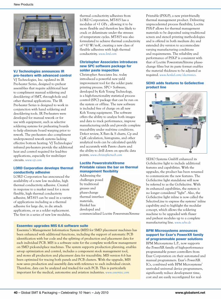
40 – Global SMT & Packaging – Celebrating 10 Years – July 2010 www.globalsmt.net
New Products
VJ Technologies announces ir pre-heaters with advanced controlVJ Technologies, Inc. updated its IR Pre-heater Series, designed to preheat assemblies that require additional heat to compliment manual soldering and desoldering of SMT, through-hole and other thermal applications. The IR Pre-heater Series is designed to work in conjunction with hand soldering and desoldering tools. IR Pre-heaters were developed for manual rework or for use with equipment, such as selective soldering systems for preheating boards to help eliminate board warping prior to rework. The pre-heaters also compliment underpowered rework systems lacking effective bottom heating. VJ Technologies’ infrared pre-heaters provide the additional heat and control required for lead-free applications, especially for multi-layer circuits. www.vjt.com
lorD corporation develops thermal conductivity adhesive LORD Corporation has announced the availability of a new low modulus, high thermal conductivity adhesive. Created in response to a market need for a more flexible, high thermal conductivity adhesive, MT-815 can be used in a variety of applications including as a thermal adhesive for large die, in die attach applications, or as a solder replacement. The first in a series of new low modulus,
thermal conductivity adhesives from LORD Corporation, MT-815 has a modulus of <1 GPa , allowing it to be more flexible and therefore less likely to crack or delaminate under the stresses of temperature cycles. MT-815 was also formulated to achieve thermal conductivity of >10 W/m-K, creating a new class of flexible adhesives with high thermal conductivity. www.lord.com
christopher associates introduces new spc software package for solder paste inspectionChristopher Associates Inc. today introduced a powerful new yield improvement tool for the solder paste printing process. SPC+ Software, developed by Koh Young Technology, is a high-functionality statistical process control (SPC) package that can be run on the system or offline. The new software is included free of charge on all new Koh Young equipment. The software offers the ability to analyze both images and data to track performance, improve manufacturing yields and provide complete traceability under real-time conditions. Defect review, X Bars & S charts, Cp and CpK calculation, histograms, and other analytical tools can be calculated quickly and accurately with Pareto charts and the ability to drill down on specific data points. www.christopherweb.com
loctite powerstrateXtreme printable raises the bar on thermal management flexibilityAddressing the challenges posed by traditional greases and phase-change thermal interface materials, Henkel has developed and commercialized Loctite PowerstrateXtreme
Printable (PSX-P), a new print-friendly thermal management product. Delivering unprecedented process flexibility, Loctite PSX-P allows for thermal management materials to be deposited using traditional screen and stencil printing methodologies and is offered in both medium dry and extended dry version to accommodate varying manufacturing conditions and requirements. The reliability and performance of PSX-P is consistent with that of Loctite PowerstrateXtreme phase-change films but its paste format enables the material thickness to be adjusted as required. www.henkel.com/electronics.
seho adds features to goselective product line
SEHO Systems GmbH enhanced its GoSelective light to include additional features and capabilities. With the upgrades, the product has been renamed to communicate the new features. The GoSelective light standalone will now be referred to as the GoSelective. With its enhanced capabilities, the system is no longer considered “light”. Also, the GoSelective light inline is now called the SelectiveLine to express the systems’ inline capability and to highlight the modular concept, which allows the soldering machine to be upgraded with fluxer and preheat modules up to a complete manufacturing line. www.seho.de
BpM Microsystems announces support for exar’s powerXr family of programmable power solutionsBPM Microsystems L.P., now supports the PowerXR family of high-performance programmable power controllers from Exar Corporation on their automated and manual programmers. Exar’s PowerXR ICs, combined with BPM Microsystems’ unrivaled universal device programmers, significantly reduce development time, cost and are easily reconfigured for real-
essemtec upgrades Mis 6.6 software suiteEssemtec’s Management Information System (MIS) for SMD placement machines has been enhanced with additional functions, including the support of automatic PCB identification with bar code and the splitting of production and placement data for each individual PCB. MIS is a software suite for the complete work-flow management on SMD pick-and-place machines. The system supports production planning, enables set-up optimization and control, includes a component stock management tool, and stores all production and placement data for traceability. MIS version 6.6 has been optimized for tracing both panels and PCB clusters. With the upgrade, MIS now saves production and assembly data with reference to each individual circuit. Therefore, data can be analyzed and tracked for each PCB. This is particularly important for the medical, automotive and aviation industries. www.essemtec.com

Global SMT & Packaging – Celebrating 10 Years – July 2010 – 41www.globalsmt.net
New Products
time design changes. BPM Microsystems supports the XRP7704 and XRP7714, a 5Amp/channel regulator, and the XRP7740, a 16 Amp/channel version, on its full line of universal device programmers. www.bpmmicro.com
count on Tools introduces selective soldering nozzles for ace equipmentCount On Tools Inc. is now manufacturing ACE Bullet nozzles for the KISS range of selective soldering machines. By utilizing superior steel alloys made in the USA, along with the latest precision machining technologies, Count On Tools is able to produce selective soldering nozzles that are more durable and last longer than those from the OEM, while still maintaining all of the original design properties. The nozzles are available in all standards sizes from 3mm (0.125”) to 25mm (1.0”). Count On Tools also provides identification marks that enable customers to easily identify lead nozzles
from lead-free versions. In addition, Count On Tools now offers custom selective solder nozzles based on specific application requirements. This includes special wave form sizes and extended or shortened lengths. www.cotinc.com
Multitest’s MT9928 platform combines roi and high efficiency
Multitest announces that its next-generation MT9928 bowl feed module
has successfully passed the strict QA and production approval requirements of an international IDM. The state-of-the-art gravity feed handler offers a variety of loading and un-loading options. With a throughput of up to 14,500 uph, the bowl feed loading module is the loading option of choice for small package sizes. The bowl feed module offers the modularity and conversion of the MT9928 platform without limiting the flexibility of the base machine. The system can be combined with all types of un-loaders, further improving the return on investment. www.multitest.com
MeMs cavity seal integrityAs part of its bonded wafer inspection
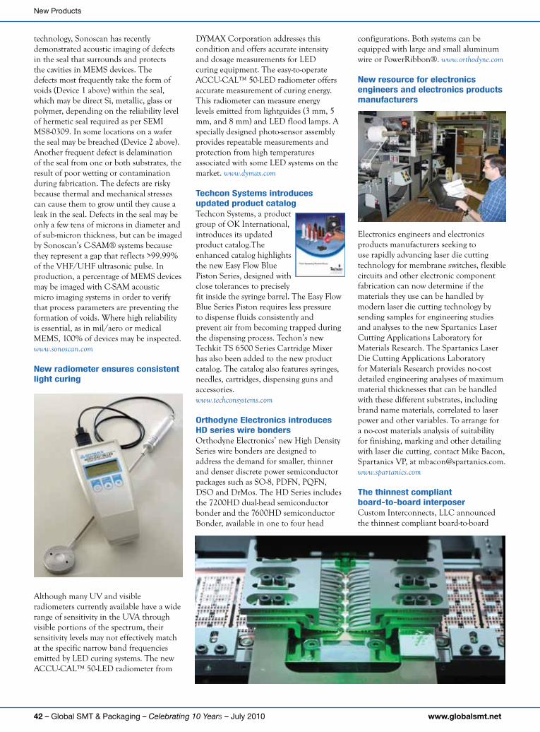
42 – Global SMT & Packaging – Celebrating 10 Years – July 2010 www.globalsmt.net
New Products
technology, Sonoscan has recently demonstrated acoustic imaging of defects in the seal that surrounds and protects the cavities in MEMS devices. The defects most frequently take the form of voids (Device 1 above) within the seal, which may be direct Si, metallic, glass or polymer, depending on the reliability level of hermetic seal required as per SEMI MS8-0309. In some locations on a wafer the seal may be breached (Device 2 above). Another frequent defect is delamination of the seal from one or both substrates, the result of poor wetting or contamination during fabrication. The defects are risky because thermal and mechanical stresses can cause them to grow until they cause a leak in the seal. Defects in the seal may be only a few tens of microns in diameter and of sub-micron thickness, but can be imaged by Sonoscan’s C-SAM® systems because they represent a gap that reflects >99.99% of the VHF/UHF ultrasonic pulse. In production, a percentage of MEMS devices may be imaged with C-SAM acoustic micro imaging systems in order to verify that process parameters are preventing the formation of voids. Where high reliability is essential, as in mil/aero or medical MEMS, 100% of devices may be inspected. www.sonoscan.com
New radiometer ensures consistent light curing
Although many UV and visible radiometers currently available have a wide range of sensitivity in the UVA through visible portions of the spectrum, their sensitivity levels may not effectively match at the specific narrow band frequencies emitted by LED curing systems. The new ACCU-CAL™ 50-LED radiometer from
DYMAX Corporation addresses this condition and offers accurate intensity and dosage measurements for LED curing equipment. The easy-to-operate ACCU-CAL™ 50-LED radiometer offers accurate measurement of curing energy. This radiometer can measure energy levels emitted from lightguides (3 mm, 5 mm, and 8 mm) and LED flood lamps. A specially designed photo-sensor assembly provides repeatable measurements and protection from high temperatures associated with some LED systems on the market. www.dymax.com
Techcon systems introduces updated product catalogTechcon Systems, a product group of OK International, introduces its updated product catalog.The enhanced catalog highlights the new Easy Flow Blue Piston Series, designed with close tolerances to precisely fit inside the syringe barrel. The Easy Flow Blue Series Piston requires less pressure to dispense fluids consistently and prevent air from becoming trapped during the dispensing process. Techon’s new Techkit TS 6500 Series Cartridge Mixer has also been added to the new product catalog. The catalog also features syringes, needles, cartridges, dispensing guns and accessories.www.techconsystems.com
orthodyne electronics introduces hD series wire bondersOrthodyne Electronics’ new High Density Series wire bonders are designed to address the demand for smaller, thinner and denser discrete power semiconductor packages such as SO-8, PDFN, PQFN, DSO and DrMos. The HD Series includes the 7200HD dual-head semiconductor bonder and the 7600HD semiconductor Bonder, available in one to four head
configurations. Both systems can be equipped with large and small aluminum wire or PowerRibbon®. www.orthodyne.com
New resource for electronics engineers and electronics products manufacturers
Electronics engineers and electronics products manufacturers seeking to use rapidly advancing laser die cutting technology for membrane switches, flexible circuits and other electronic component fabrication can now determine if the materials they use can be handled by modern laser die cutting technology by sending samples for engineering studies and analyses to the new Spartanics Laser Cutting Applications Laboratory for Materials Research. The Spartanics Laser Die Cutting Applications Laboratory for Materials Research provides no-cost detailed engineering analyses of maximum material thicknesses that can be handled with these different substrates, including brand name materials, correlated to laser power and other variables. To arrange for a no-cost materials analysis of suitability for finishing, marking and other detailing with laser die cutting, contact Mike Bacon, Spartanics VP, at [email protected]. www.spartanics.com
The thinnest compliant board-to-board interposerCustom Interconnects, LLC announced the thinnest compliant board-to-board

Global SMT & Packaging – Celebrating 10 Years – July 2010 – 43www.globalsmt.net
New Products
interposer ever developed: the Thinnerposer®. The Thinnerposer® is expected to draw a great deal of interest from the RF design community. Targeted applications for the new Thinnerposer® technology include UAV/UAS, avionics, radar arrays, space probes and orbital satellites—a natural fit for the superior flexibility, impedance matching, and shock/vibration attributes of this product set. www.custominterconnects.com
Boundary scan tools keep on developing
JTAG Technologies announced further advances in the boundary-scan tool arena with the latest release of its development and hardware debug tool, JTAG ProVisionT V1.8, that features on the latest tools CD (release 16 - May 2010). ProVision combines advanced automation with the level of control and precision that engineers demand when creating test programs and in-system programming (ISP) routines for PLDs, FPGAs, flash memories, serial PROMs and other devices. Enhancements to the ProVision version (V1.8) include new pin-level ActiveTest, multi-board and scan bridge support for JFT (Python) script routines, and an expanded ProVision model library covering more than 78,00 devices. www.jtag.com
The stock you need, when & where you need it; paragon VMi service cuts cost of component supplyIn the wake of recent economic challenges, the pressure is on manufacturers to find new ways to remain competitive. Against this backdrop, Bedford-based Paragon’s Vendor Managed Inventory (VMI) service is fast becoming the supply chain management service of choice for production environments in the UK and beyond. Part of Paragon’s Total
Component Management™ (TCM™) solution, the company’s VMI service is central to its belief that OEMs can gain substantial benefits by outsourcing procurement, supply chain management and logistics to a specialist company. With their VMI service, Paragon establishes line side stores at customer premises, enabling instant access to high volumes of parts, on-site. Available as ‘consigned stock’, these parts are only invoiced for when used, reducing customer risk and streamlining supply. Not only does VMI significantly improve cash flow and improve stock
availability, but it reduces acquisition costs through reduced material handling and eliminating the need for multiple purchase transactions and processing multiple invoices. www.paragon-kitting.com
single component snap cure epoxy has outstanding electrical properties and chemical resistanceMaster Bond EP17HT-3 is a one part epoxy that sets
New Horizons in Bond Testing
Data IntegrityDeveloped by the world leader in bondtesting technology, the 4000Plus offers unsurpassed accuracy and repeatability of data providing complete confidence in results.
Extensive Testing CapabilityLoad cartridges combined with standardand specialized fixtures perform shear tests up to 500kg, pull tests up to 100kgand push tests up to 50kg, covering all your test applications including new hotbump pull and fatigue applications.
Ultimate VersatilityA range of XY stages, with a 160mm XY stage as standard, meets a wide range of requirements. The image capture system for advanced analysis is quick to set-up and in close proximity to the test head aiding faster testing.
www.nordsondage.com | [email protected]
See the 4000Plus bondtester in action at Semicon West 2010: Booth No. 5947
The Nordson DAGE 4000Plus is the most advanced
bondtester on the market, representing the
industry standard in bond testing.
Intelligent SoftwareThe 4000Plus utilizes Nordson DAGE’s next generation Paragon™ software whichboasts a highly configurable and intuitive interface as well as a wide variety of advanced functionality such as automaticGR&R calculation, built-in diagnostics, aunique database search engine wizard andsuperior reporting.
Learn more at www.nordsondage.com/4000Plus
Global SMT AD:Layout 1 2/6/10 12:03 Page 1

44 – Global SMT & Packaging – Celebrating 10 Years – July 2010 www.globalsmt.net
New Products
up in 20 to 30 seconds and snap cures in only 2 to 3 minutes at 250°F-300ºF. As a one-part system, no mixing is required and the epoxy can be cured in sections up to ¼-inch thick. Moreover, its working life is indefinite as it will not gel until heated above 200ºF. With a volume resistivity of greater than 1014 ohm-cm, EP17HT-3 has excellent electrical insulation and chemical resistance characteristics. It also has superior temperature resistance with a service operating temperature range of -60ºF to +400ºF. It is 100% reactive and contains no solvents or diluents. www.masterbond.com
intertronics unveils “greeN” Techspray renew™ cleaners
Intertronics announced a new range of environmentally friendly Techspray Renew products. Two innovative products are designed specifically for a range of industrial applications from engineering to electronics and laboratories to offices: Eco-
Shine™ glass and surface cleaner and Eco-Shower™ cleaner and degreaser. Both are effective, safe and eco-friendly, and feature the following advantages: Non-flammable; biodegradable; low VOC, zero GWP; non-ozone depleting. The benefits of the Renew product line include low ecological impact, low VOCs and no global warming, sustainable and biodegradable, recycled/recyclable packaging and regulatory compliance—they fully meet European REACH and WEEE requirements. www.intertronics.co.uk
Verigy announces mixed-signal testing capability for V101 platform
Verigy has enhanced its V101 platform by adding new capability for testing mixed-signal semiconductor devices. The versatile V101 platform, designed for high-volume testing of cost-sensitive ICs at both the wafer sort and final test production steps, now delivers mixed-signal capability designed for testing devices with audio and video signals. The V101’s mixed-signal capability is enabled by a plug-and-play module that can be quickly and easily installed into the V101 for testing mixed-signal ICs used in applications such as automotive, communications, data processing, and audio and video consumer electronics. The zero-footprint V101 platform can cost-effectively test microcontrollers and other low-pin-count, low-cost ICs in the high-mix manufacturing environments where these devices are typically produced. www.verigy.com
absolute Turnkey introduces absolute advantage program to the oeM and eMs marketplaceAbsolute Turnkey announces the Absolute Advantage program for OEMs and the EMS marketplace. The Absolute Advantage program was developed to provide customers with the ultimate in flexibility, while getting their products

Global SMT & Packaging – Celebrating 10 Years – July 2010 – 45www.globalsmt.net
New Products
to market with speed. The combination of flexibility and speed is what sets the Absolute Advantage apart from other EMS providers.The Absolute Advantage helps customers to rapidly introduce innovative technology, which provides a speed-to-market solution for OEM customers. The complete solution also provides speed in getting OEM customers’ products to market quickly. The end-to-end solution is ideal for engineering services, prototypes, pilots and production. www.AbsoluteTurnkey.com
Multi-seals now offers epoxy preforms with low outgassing properties Multi-Seals Inc. introduces a line of Uni-form epoxy preforms with low outgassing properties. Unlike many adhesives, these highly cross-linked pre-shaped thermoplastics release minimal amounts of trapped gasses or condensable material under vacuum conditions and elevated heat.
Low outgassing properties are essential for aerospace applications, particularly in vacuum environments where volatiles from other adhesives often condense on optics and electronics, adversely affecting their function. With a typical total mass loss of 0.35% and typical collected volatile condensable materials of 0.03% (tested per ASTM-E-595-93), these low-outgassing epoxies meet NASA requirements for most spacecraft materials. www.multi-seals.com
guide to understanding electrical Test and Measurement
Keithley Instruments, Inc. released a tutorial CD that offers practical and helpful techniques for obtaining the most accurate and precise measurements
possible. Keithley’s “A Guide to Understanding Electrical Test and Measurement” CD is the most in-depth knowledge center that Keithley has ever created, and covers all aspects of measurement performance, including how to troubleshoot, how to connect, how to select instruments and much more. The CD contains a large number of application notes, white papers and webcasts on a wide variety of test and measurement topics.To receive your free copy of Keithley’s A Guide to Understanding Electrical Test and Measurement CD, visit www.keithley.info/tmcdfy10
For beautiful marking results—fastTRUMPF introduces two new marking lasers—the TruMark 6030 and TruMark 6140—to its TruMark Series 6000. Users can now choose from six high performance machines that are available in any wavelength needed for surface processing. The TruMark 6030 and 6140 lasers feature considerably shorter marking times when compared to other products in the TruMark Series 6000. TRUMPF has increased the output of these new marking lasers by about 35 percent. www.trumpf.com

46 – Global SMT & Packaging – Celebrating 10 Years – July 2010 www.globalsmt.net
Case Study: High quality manufacturing need not mean high production costs
While purely technical treatments of reliability issues are important, it also is important to understand why some of the developments impacting our industry came about. The development of ball grid array (BGA) components as well as column grid array (CGA) components is such a case.
BGAs and CGAs came about because the solder attachments of leadless ceramic chip carriers (LLCCCs) on FR-4 PCBs could not meet reliability requirements.
The first large surface mount (SMT) component was the leadless ceramic chip carrier (LLCCC), with solder joints
formed by bottom soldering pads and soldering areas in ‘castellations’ along the sides. These castellations were the result of the postage-stamp-like perforations of the ceramic in its green stage prior to separation by breaking. As all components in that time frame, it was made of ceramic to be soldered to hybrid substrates, also made of ceramic. That, of course, did not last, and LLCCCs were placed on FR-4 PCBs as well, with the in hindsight fully understandable problem with inadequate solder joint reliability1 as can be seen in Figure 1.
Lots of effort went into trying to improve the solder joint reliability of this combination2, see Figure 2.
However, for leadless solder joints, there are only four primary parameters determining solder joint reliability:
1. component size, DNP (distance from neutral point)
2. the mismatch in coefficients of thermalexpansion,∆CTE;
3. thecyclicthermalexcursion,∆T;and
4. the solder joint height, h.For ceramic components on FR-4, the
∆CTEisessentiallyfixed;thecomponentsize determining the DNP is a function of functionality,asis∆T—thatleavesonlyh.Everything else being equal, the cycles-to-failure increase roughly with the power-of-two of the solder joint height, h.
Thus, at Bell Laboratories, both solder balls and solder columns were utilized to increase h; mind you those initial components had only peripheral rows of
Werner Engelmaier
A history of the development of ball grid array (BGA) and column grid array (CGA) components
A history of the development of ball grid array (BGA) and column grid array (CGA) components
“BGAs and CGAs came about, because the solder attachments of leadless ceramic chip carriers (LLCCCs) on FR-4 PCBs could not meet reliability requirements.”
Figure 1. Fatigued solder joints of leadless ceramic chip carrier on FR-4 (Courtesy of Dave Hillman, Rockwell Collins, USA).
Figure 2. Fatigued ‘ bulbous’ solder joints of leadless ceramic chip carrier on FR-4 (Courtesy of Gail Love, Martin-Marietta, Florida USA).

Global SMT & Packaging – Celebrating 10 Years – July 2010 – 47www.globalsmt.net
soldering pads since they were LLCCCs3-6. Only somewhat later a second row was added. We certainly did not call them the ‘array-anything’ initially, because at that stage they were not arrays. The results of exhausting reliability testing were published rather late because of misplaced management competitive concerns7. Figures 3 and 4 show the first fatigued solder balls and solder columns.
Because of the origin as LLCCCs, the initial soldering pads, both on the components and the PCBs, were not circular, but rectangular or square. Circular pads were only introduced because of the solder columns. Results from accelerated tests show that the solder joint geometries produced by rectangular soldering pads result in slightly higher fatigue lives than those from circular pads7.
The insights gained led to the commercialization of BGAs and CGAs; it also led to the development of high-melting 90Pb10Sn solder balls which would not melt and collapse during reflow soldering, thus maintaining the ball diameter as the solder joint height, h. With the soldering temperatures for the Pb-free solders, this technology is no longer available, however, and an alternate technology8 works at least as well.
references:1. Engelmaier, W., “Effects of Power
Cycling on Leadless Chip Carrier Mounting Reliability and Technology,” Proc. Int. Electronics Packaging Conf. (IEPS), San Diego, CA, November 1982, p. 15.
2. Engelmaier, W., “Of Ceramic Components: Failed Solder Joints, LLCCCs, ‘Bulbous’ Solder Joints, ‘Super-Compliant’ Leads, and
Forgotten Lessons,” Global SMT & Packaging, Vol. 3, No. 2, March 2003, pp. 42-43.
3. Hall, P. M., “Forces, Moments, and Displacements During Thermal Chamber Cycling of Leadless Ceramic Chip Carriers Soldered to Printed Boards,” IEEE Trans. Components, Hybrids, and Manufacturing Technology, Vol. CHMT-7, No. 4, December 1984, p. 314.
4. Fisher, J. R., “Cast Solder Leads for Leadless Semiconductor Circuits,” U.S. Patent 4,412,642, November 1, 1983.
5. Fisher, J. R., “Cast Leads for Surface Attachment,” Proc. 44th Electronic Components Conf., New Orleans, LA, May 1984, pp. 487-497; also in IEEE Trans. Components, Hybrids, and Manufacturing Technology, Vol. CHMT-7, No. 4, December 1984, pp. 306-313
6. LoVasco, F., and M. A. Oien, “A New Soldering Technology for Surface-Mounting Pad Grid Arrays,” Proc. Int. Electronics Packaging Conf. (IEPS), November 1988.
7. Engelmaier, W., “BGA and CGA Solder Attachments: Results of Low-Acceleration Test and Analysis,” Proc. Surface Mount International Conf., San Jose, CA, August 1995, pp. 344-358; also in Proc. Int. Electronics Packaging Conf. (IEPS), San Diego, September 1995, pp. 758-774; also in Proc. NEPCON West ‘96, Anaheim, CA, February 1996, pp. 385-395.
8. Engelmaier, W., “Achieving Solder Joint Reliability in a Lead-Free World, Part 2,” Global SMT & Packaging, Vol. 7, No. 7, July 2007 [EU-edition], pp. 48-50; No. 8, August 2007 [US-edition], pp. 44-46.
Werner Engelmaier will be giving some of his reliability workshops at Conferences in Tallinn,
Estonia, September 21-23, 2010 and GEM Expo Brazil 2010 in Sao Paolo, Brazil, October
5-7, 2010. He will be available for in-house workshops and consulting in both English and German in Europe in the June timeframe; for
details of the workshops go to www.engelmaier.com; for more information about the workshops
and consulting contact [email protected].
Werner Engelmaier has over 44 years experience in electronic packaging and interconnection
technology and has published over 200 papers, columns, book chapters and White Papers. Known as ‘Mr. Reliability’ in the industry,
he is the president of Engelmaier Associates, L.C., a firm providing consulting services on
reliability, manufacturing and processing aspects of electronic packaging and interconnection technology. He is the chairman of the IPC
Main Committee on Product Reliability. The TGM-Exner Medal was bestowed on him in 2009 in Vienna, Austria, he was elected
into the IPC Hall of Fame 2003, and was awarded the IPC President’s Award in
1996 and the IEPS Electronic Packaging Achievement Award in 1987. He also
was named a Bell Telephone Laboratories Distinguished Member of Technical Staff in
1986 and an IMAPS Fellow in 1996. More information is available at www.engelmaier.com, and he can be reached at engelmaier@
aol.com.
A history of the development of ball grid array (BGA) and column grid array (CGA) components
Figure 3. Fatigued solder ball from a ceramic BGA on FR-4 (Source: Werner Engelmaier, Bell Laboratories, USA).
Figure 4. Fatigued solder columns from a ceramic CGA on FR-4 (Source: Werner Engelmaier, Bell Laboratories, USA).

48 – Global SMT & Packaging – Celebrating 10 Years – July 2010 www.globalsmt.net
Case Study: High quality manufacturing need not mean high production costs
Association & institutes news
sMarT group announce 26th Birthday conferenceFollowing our successful two-day conference last year that celebrated 25 years of the SMART Group’s existence, SMART Group proudly announces that after a busy year of events, they will celebrate their 26th anniversary with an equally exciting two-day event.
The aim and thrust of this year’s conference is to address many of the issues facing our industry today. Despite some of the pessimism, the electronics industry here has much still to offer our global customers.
As an example, SMART Group’s vice chair, Graham Naisbitt, quoted a recent statement issued by the Chinese government that they were concerned that their industry has a poor reputation for quality and reliability.
“They sponsored a delegation to come to the UK, through ITRI, International Tin Research Institute in St Albans,” Naisbitt said, “where a number of persons would make presentations to them on this topic. In particular I was thankful that they consider the UK is still the centre to develop products that have high quality and high reliability.
“Shame only that we no longer seemingly have the capacity to produce in large quantities, perhaps that will change.”
This year’s conference will look at the supply chain, inform about the latest research projects and explore whether manufacturing standards make things better. Other topics cover production control, the importance of chemistry, what’s happening with RoHS and REACH, why do we clean when we have no clean and what are tin whiskers—all will be explained. The sessions will also cover component tinning and re-tinning good practice, silver vs sulphur—can conformal coating help?
We are lining up an eminent world-class team for this event to be held on 6th & 7th of October. The venue is again The Oxfordshire GC Business Centre.
The full programme of presentations will be announced shortly with a list of exhibitors.
For more information contact: Tony Gordon, SMART Group Secretary, Tel: +44 (0)1494 465217 Email: [email protected] or Mike Judd, SMART Group PR Director, Tel: +44 (0)118 978 4589 Email: [email protected].
european parliament environment committee vote puts TBBpa on priority assessment listIPC—Association Connecting Electronics Industries® expressed disappointment in the vote by the European Parliament’s Environment Committee to include broad families of chemicals, such as organobro-mines, in Annex III for priority assessment. While an outright ban of these chemicals has been averted in this vote, the commit-tee’s decision falls far short of supporting a rigorous scientific assessment that would ensure protection of the environment and human health.
IPC is concerned that the process outlined in the amendments approved today does not define a rigorous scientific methodology. The proposed process “lacks a rigorous scientific methodology and could therefore lead to additional substance restrictions that provide neither environmental nor human health benefits,” says Fern Abrams, IPC director of environmental policy and government relations.
The inclusion of broad families of chemicals, such as all organobromines, for priority assessment under Annex III is impractical and unscientific. While some organobromines, such as polybrominated biphenyls (PBBs), have been identified as toxic, restricted under the RoHS Directive and voluntarily withdrawn from the market, other organobromines, such as TBBPA, have been found to be safe for human health and the environment by both the World Health Organization and the European Commission Scientific Committee on Health and Environmental Risks (SCHER).
In direct lobbying efforts over the past year, IPC has urged the European Union to amend the RoHS Directive to introduce rigorous scientific methodology aligned with the comprehensive chemicals evaluations under the REACH (Registration, Evaluation, Authorisation and Restriction of Chemicals) regulation.
IPC continues to lobby to ensure the RoHS revision’s process reflects sound scientific methodology. IPC’s white paper, “Recasting the RoHS Directive: An Opportunity to Solidify its Scientific Basis in Support of Comprehensive Environmental Regulation,” advocates for a revised RoHS to be based on sound science and fully aligned with the REACH methodology for substance restrictions.
The European Parliament is currently scheduled to vote in July on the Environment Committee’s recommendations for recasting the RoHS Directive. The Environment Committee is also scheduled to vote on the related Waste Electrical and Electronic Equipment (WEEE) Directive later this month, with a plenary vote to take place in July. www.IPC.org
ipc-2152-De—standard for deter-mining current-carrying capacity in printed board design now available in german IPC - Association Connecting Electronics Industries® announced the German lan-guage release of IPC-2152-DE, Designrich-tlinie für die Bestimmung der Stromtrag-fähigkeit von Leiterplatten. This document is the translation of IPC-2152, Standard for Determining Current-Carrying Capac-ity in Printed Board Design, which was released in English in August of 2009. The 97-page document sets the sole industry standard for determining the appropriate sizes of internal and external conductors as a function of the current-carrying capac-ity required and the acceptable conductor temperature rise.
IPC members may request a free, single-user download of IPC-2152-DE by e-mailing [email protected] within 90 days of its release; after 90 days, the price for members is $50. The nonmember price of IPC-2152-DE is $100. Visit www.ipc.org/2152-DE for details and to purchase.
Association & institutes news

Global SMT & Packaging – Celebrating 10 Years – July 2010 – 49www.globalsmt.net
Title

50 – Global SMT & Packaging – Celebrating 10 Years – July 2010 www.globalsmt.net
IMAPS Europe newsNews from iMaps italyOn the 20th of May, IMAPS Italy held a workshop on cleaning technologies for electronic assembly at the Crown Plaza hotel San Donato Milan. The event was held in association with Assodel, the Ital-ian electronic suppliers association, and sponsored by AMES, the microelectronic and semiconductor section of the Italian Electronic and Electrical Association. Over 60 participants attended from 46 technical institutions and companies representing a cross section of companies involved in electronic component and system manu-facture. Presentations were given on the potential hazards caused by contaminants in microlectronic assemblies and the iden-tification of associated failure mechanisms, cleaning methods including new develop-ments solvents and plasma cleaning. A par-ticularly interesting problem was outlined by L. Ferruccci of Nokia Siemens Networks showing how miniscule flux residues can vary RF performance.
News from iMaps Nordic IMAPS Nordic has an old tradition to hold their yearly conference alternating in each of the four Nordic countries. This year Swe-den was in tour and Gothenburg on the west coast was chosen as a lot of electronics industry and research is located here. The programme was very rich, with both local speakers and invitees from other regions. Among the best was Jean-Marc Yannou’s presentation on 3D packaging and IPDs. The ELC President Nihal Sinnadurai brought us both technical information and news about the organisational situation within Europe and globally. The event was finished with a visit to IMEGO Institute where applied research and new electron-ics products are pre-developed in close cooperation with both industry and other R&D institutes.
Unfortunately the participation in the conference was lower than ever. This could be due to the fact that this was the first time it was held in June, not September. Perhaps the organisers were not alert to market the event early enough, or is June not a good time for the participants? Next year we will try June again, this time in Finland.
News from iMaps polandThe 34th IMAPS-CPMT Poland 2010 International Conference organized by Wroclaw University of Technology (Faculty of Microsystem Electronics and Photon-ics) will be held in Wroclaw on 22-25 September, 2010. This year our conference is organized together with 10th Electron Technology ELTE 2010 Conference (Polish conference organized every three years and devoted to electronic materials, micro- and nanoelectronics, photonics and micro-systems). It will be a good opportunity to exchange the scientific results between wide range of scientists and specialists from elec-tronic industry. The conference presenta-tions will be divided into plenary sessions, section sessions and poster sessions.
The main topics include:• Thin- and thick-film technologies; • Thin- and thick-film sensors; • Modelling, design and simulation
of film structures, components and circuits;
• Modern technologies and applications of multichip modules;
• Electrical, optical, mechanical and thermal characterization of film structures, components and circuits;
• Packaging in electronics, photonics and microsystems;
• Quality and reliability of film structures and packaging processes.
The exhibition of technological and diagnostic equipment is planned during the conferences. Papers chosen by scien-tific committees will be recommended for publishing in international and national technical journals.
The conference presentations will be divided into plenary sessions, section sessions and poster sessions. Presentations/posters for IMAPS/CPMT will be prepared in English abstracts, and full texts of papers will be prepared in English. Students, PhD students and young researchers (below 32 years old) can participate in contests for best papers in particular thematic sections.
Exhibition of technological and diagnostic equipment is planned during the conference.
Papers chosen by the Scientific Committees will be recommended for publishing in international and national technical journals.
The conference will be held at the Wrocław University of Technology, building C-13, i.e. Integrated Students Center, Wybrzeże Wyspiańskiego 23/25 in Wrocław
More information can be found on the conference website: www.imaps2010.pwr.wroc.pl.
IMAPS news
Conference building (C-13) at Wrocław University of Technology . (Source: Maciek Krol)

��������������������������������
OctOber 5-7, 2010—eXPO ceNter NOrte, SãO PAULO, brAZIL
www.gemexpobrazil.com
Sponsors VenueOrganizer
goal! New opportunities await at the only dedicated electronics manufacturing event in South America.
• IPC Training & Certification • Advanced training workshops • Vendor Conference • Exhibition
September 21-23, 2010 | Tallin, Estonia | www.europeanelectronicsummit.com
The European Union continues to impose legislation on the electronics manufacturing community. REACH, RoHS and WEEE all have significant impact on the manufacturability of our board assemblies and finished goods.
The Second European Electronics Assembly Reliability Summit brings together experts and provides a unique opportunity to examine, learn and debate these business-critical issues through industry discussion, technical collaboration and information sharing. The event will include a technical conference, tabletop exhiibition and networking opportunities.
Join us this September. Visit the website to learn more.
This conference is being held at a critical time for the electronics industry.
Increasing legislation and lack of reliability in electronics assemblies and
interconnections is providing many challenges for, designers, specifiers and
manufacturers of printed assemblies. The rise in counterfeit components is only
adding to these challenges.
European Electronics Assembly
Reliability SummitSeptember 21-23, 2010
Tallink Spa & Conference Hotel, Tallin, Estonia

Title
52 – Global SMT & Packaging – Celebrating 10 Years – July 2010 www.globalsmt.net
International Diary13-15 July Semicon WestSan Francisco, Californiawww.semiconwest.org
7-10 September electronica India/productronica India Bangalore, Indiawww.productronica-india.com
15-17 September GlobalTRONICS Singaporewww.globaltronics.com.
28-20 September IPC Midwest Conference & Expo Schaumburg, Illinois, USAwww.ipcmidwestshow.com
5-7 October GEM Expo Brazil São Paulo, Brazilwww.gemexpobrazil.com
24-28 October SMTA International Orlando, Florida, USAwww.smta.org/smtai
31 October-4 November IMAPS Symposium Raleigh, North Carolina, USAwww.imaps2010.org
9-12 NovemberelectronicaMunich, Germanywww.electronica.de
30 November-2 DecemberPrinted Electronics USASanta Clara, California, USAwww.idtechex.com/ printedelectronicsusa10/pe.asp
Other editions
China
www.globalsmt.net
SMTSMT
Korea
www.globalsmtindia.in
Volume 1 number 2 summer 2010
neW ProDucts
InDustrY neWs
InternatIonal DIarY
global SMT &
packaging South east asia Vol. 1 No. 2Sum
mer 2010
South East AsiaSouth East Asia
NANOTECHNOLOGY IS NOW STARTING TO FIND APPLICATIONS IN ELECTRONICS
HEAD-IN-PILLOW: IDENTIFYING AND HIGHLIGHTING SUSPECT SOLDER JOINTS
BGA ASSEMBLY RELIABILITY—PWB QUALITY IS THE KEY
Erik MillerInterview Inside
covering India, thailand, malaysia, singapore, the Philippines and hong Kong
1.2.indd 1 5/14/10 10:52 AMSouth East Asia
The Global Assembly Journal for SMT and Advanced Packaging Professionals
Volume 10 Number 7 July 2010
ISSN 1474 - 0893
www.globalsmt.net
The Global Assembly Journal for SMT and Advanced Packaging Professionals
ISSN 1474 - 0893
David RabyInterview Inside
NEW PRODUCTS
INDUSTRY NEWS
INTERNATIONAL DIARY
False top coatings oF a counterFeit component revealed layer by layer
WaFer-level solder sphere placement and its implications
steps toWard closing the soFtWare quality gap
David RabyInterview Inside
NEW PRODUCTS
INDUSTRY NEWS
INTERNATIONAL DIARY
False top coatings oF a counterFeit component revealed layer by layer
WaFer-level solder sphere placement and its implications
steps toWard closing the soFtWare quality gap
Volume 10 Number 7 July 2010
North America
Including the European edtion that you’re reading right now, Global SMT & Packaging carries its message across five editions and six continents. For information on advertising opportunities in any or all of our editions, contact your local sales rep.
Americas—Derek Laborie Tel: +1 (239) 245-9264 [email protected]
europe—Andy KellardTel: +44 7766 [email protected]
Asia/Pacific—Nitesh MadanTel: [email protected]

Act now for 2 free issues
Special Subscription Offer
Please send me a two-month complimentary subscription. If I do not cancel within 90 days, I will receive the magazine Global SMT & Packaging for one year (12 issues) for a special price of $72.
Trafalgar Publications Ltd.8 Talbot Hill Road, Bournemouth, Dorset BH9 2HJ, United KingdomPhone: +1 866-948-5554, Fax: +1 [email protected], www.globalsmt.net
Volume 9 Number 10 October 2009ISSN 1474 - 0893
The Global Assembly Journal for SMT and Advanced Packaging Professionals
Mike ScimecaInterview Inside
NEW PRODUCTS
INDUSTRY NEWS
INTERNATIONAL DIARY
What you need to knoW before buying your aoi solution
Which tools are best for sMt reWork—conduction or convection?
business process ManageMent for iMproved productivity and custoMer satisfaction
www.globalsmt.net
The Global Assembly Journal for SMT and Advanced Packaging Professionals
Volume 9 Number 9 September 2009
ISSN 1474 - 0893
Mike NelsonInterview Inside
NEW PRODUCTS
INDUSTRY NEWS
INTERNATIONAL DIARY
PoP (Package on Package) and vaPor Phase technology
a baseline study of stencil and screen Print Processes for wafer backside coating
fatigue & creeP wearout in electronics: a historical retrosPective
sPecial Packaging feature:
imbedded component/die technology (ic/dt®): is it ready for mainstream design applications?
Plus: ic packaging and interconnection technologies’ 4th dimension challenge
Assembly/Packaging EngineerCorporate/General ManagementManufacturing/Engineering ManagementResearch DevelopmentHR ManagerDesignPurchasingSales & MarketingQuality ControlEngineering SupportOther
Electronics Mfg—OEMElectronics Mfg—ContractorElectronics Mfg—DesignElectronics Mfg—SupplierMicroelectronics ManufacturerMicroelectronics ServicesMicroelectronics supplierPCB ManufacturerPCB ServicesPCB SupplierOther
Job title/Function
Primary business type
Name on card:
Number:
Expiration date: Security code:
Please check that your details are complete.
Date Signature
Company:
Name:
Job Title: Department:
Address:
City: State/Province: Zip Code:
Country:
Phone: Fax:
Email:
Web site:
Bank transfer VISA AMEX Mastercard
I will pay after receiving the invoice by:
GSP9.11
Mail, fax or email to:

Title
54 – Global SMT & Packaging – Celebrating 10 Years – July 2010 www.globalsmt.net
Smart companiesuse Valor.
smart manufacturing just got smarter
Gerd Koschnick,Manager of Process Technology
Natalia Telwa, SMT Process Manager
Peiker, one of the leading suppliers of components in the sector of communication technologies in vehicles as well as for professional radio applications, recently implemented Valor’s vManage manu-facturing execution software suite in their manufacturing facility in Germany. The implementation of the software in Germany was a success, so that Peiker decided to deploy vManage in their manu-facturing facility in Juarez Mexico, as well. Gerd Koschnick, Manager of Process Technology for Peiker, said: “The traceability requirements in the automotive industry are strin-gent. We needed a solution which could satisfy all our traceability regulations without adding to the unit costs, and also provides instant visibility into the chain of data from component lot codes to individual PCBs to final product assembly.” Natalia Telwa, SMT Process Manager, added: “What we did not realize was the added value we would receive from Valor’s trace-ability solutions. Not only do we have immediately accessible and accurate component trace data, but the vManage system also delivers closed loop control of our SMT machine feeder setups, low level warnings to trigger supply of replacement reels and real-time monitoring of our SMT line performance. So we are cutting down-time and improving productivity which lowers our unit costs. Plus: we have the traceability we needed in the first place.” Mr. Koschnick summarizes: “Implementing vManage in Germany was a smart decision. Now we are going to grow the benefits by expanding the deployment to our facility in Mexico.
www.Valor.com
MW-VA-30-203x275.indd 1 6/24/10 1:24 PM