Embed Size (px)
Citation preview

2012Annual Report
F R A U N H O F E R - E i N R i c H t U N g F Ü R M O d U l A R E F E s t k ö R p E R - t E c H N O l O g i E N E M F t

Editorial notes
published by:
Fraunhofer EMFT
Hansastrasse 27d
80686 München
Tel.: +49 (0) 89 54759-0
Fax.: +49 (0) 89 54759-550
director of the institution:
Prof. Dr. rer. nat. Christoph
Kutter
Tel.: +49 (0) 89 54759-506
Editors:
Pirjo Larima-Bellinghoven
Simone Brand
Tina Möbius
Articles were written by
Fraunhofer EMFT staff.
Publication of any material is
subject to editorial authori-
zation.
layout/typesetting:
Simone Brand
photography:
BPhoto copyright p. 39 MEV
database
All other photo copyrights
held by Fraunhofer EMFT
and Bernd Müller Fotografie,
Maximilianstrasse 56, 86150
Augsburg.
© Fraunhofer EMFT 2013

3
F R A U N H O F E R E M F t
AnnuAl RepoRt 2012

4
/ / V O R w O R t/ / F O R E w O R d

5
dear friends and partners of the Fraunhofer Research
institution for Modular solid state technologies EMFt,
dear readers,
A lot happened at the Fraunhofer EMFT last year. I took up my
position as institution director on July 1st. In August, the new
division director Prof. Maurer started setting up the „Circuits
and Systems“ area. In Autumn a strategy process was initiated
to sharpen the institution‘s profile: „Fraunhofer EMFT stands
for cutting-edge applied research into sensors and actuators
for man and the environment.“ Fraunhofer EMFT bases its
research initially on customer needs in the area of sensors and
actuators: The technology decision, whether to fabricate the
sensor in silicon of flexible technology comes second.
The following core competences form the basis of the research
work at Fraunhofer EMFT: silicon technology (individual
processes and integration), flexible electronics, chemical sensor
materials and the ability to create systems. Each of these core
competences in its own right allows new kinds of sensors and
actuators to be created. But the real strength of Fraunhofer
EMFT lies in the interaction between these areas: after all,
innovations often emerge where technologies reach their
borders and begin to cross-fertilize. For example, ultrathin
silicon chips can be integrated in foil to create new lab-on-
chip applications. Integration of chemical sensor dyes with
interdigital capacitors in silicon or polymer technology enables
electrical analysis of the optical signals emitted by the dyes.
It is often no longer sufficient to develop a good component:
the element must be capable of working within the system or
application, too. This is why system expertise and the ability
to integrate technologies and components are becoming
increasingly important to our institution.
The well-established network with universities in Munich
and Regensburg enables Fraunhofer EMFT to supplement its
expertise.
Dear readers, Fraunhofer EMFT is in a state of change. We are
moving towards:
• being more closely geared to applications: research
themes are derived from customer needs
• a clear profile: sensors and actuators for man and the
environment
• further expansion of the core competences: sensor
materials, individual silicon processes and integration,
flexible technologies and the ability to integrate systems.
I hope you enjoy reading our annual report and I would
eagerly look forward to the opportunity to collaborate on
many more joint projects next year.
Yours sincerely,
Prof. Dr. Christoph Kutter
Director of the Fraunhofer Research Institution for Modular Solid
State Technologies EMFT
FoReWoRD

6
/ / t A B l E O F c O N t E N t s
tAble oF contents
// Overview 6
Fraunhofer EMFT 7
History 7
Profile 7
Organigram 8
Fraunhofer EMFT - Division directors 9
The institution in figures 10
Advisory Board 11
// Business Areas 12Business areas with examples of projects 13
Sensor Materials 13
Sensors and Actuators 14
Microdosage Systems 16
Flexible Systems 18
Design and Test 20
//core competences 22Overview of core competences 23
Functional Molecules and Surfaces 23
Silicon Processes, Device and 3D Integration 24
Heterointegration and Foil Technologies 25
Systems and Prototypes 27
// Research fields and services 28Fraunhofer EMFT range of services 29
Fraunhofer EMFT range of technologies 30

7
// customers an cooperation partners 32Technology networks 33
Industry and project partners 34
European community projects 36
Universities 39
Visitors and delegations 41
Bavarian Innovation Clusters 42
// Highlights 44Special Events 45
Award of honorary doctorate 45
A scientific challenge met with excellence 45
// Events and youth development 46Events and workshops 47
Seminars and training programs 48
Trade fairs 49
Youth development 50
Careers at Fraunhofer EMFT 53
// press and media 54
// Academic puplications and talks 66
// patents 72
// Memberships and activities 74

8
1 Fraunhofer EMFT
entrance
1
/ / O V E R V i E w

9
FRAunhoFeR eMFt
History
Fraunhofer EMFT originales from the Fraunhofer Institute for
Solid State Technology IFT, which was founded in 1974.
Here, technologies were developed for the manufacture of
semiconductors.
Other areas of activity were sensor technology, communica-
tion technology and microstructure technology.
In 1999 the Fraunhofer IFT was dissolved and split into three
independent sections. The section located in Hansastrasse,
Munich - today‘s Fraunhofer EMFT - initially became part
of the Berlin-based Fraunhofer Institute for Reliability and
Microintegration IZM.
Fraunhofer EMFT was founded on July 1, 2010, as an inde-
pendent institution once again, created from the Fraunhofer
Institute for Reliability and Microintegration IZM, Munich
branch.
Profile
In its research and development work, Fraunhofer EMFT
focuses on sensors and actuators for man and the environ-
ment. Sensors already have a key role to play in our digitized
world and will become increasingly important in the years to
come as a result of the interconnection of devices („Internet
of Things“). People may not actually notice the sensors, but
they will make a significant contribution to improving the
quality of living - whether in health and nutrition, mobility or
material analysis. Fraunhofer EMFT actuators will be used in
micropumps and microvalves in medicine and industry, for
example.
In defining its research fields, Fraunhofer EMFT always
attaches priority to practical application. The institution gets
together with customers to assess areas which are important
for the market and where Fraunhofer EMFT can make a
significant contribution with its expertise. The aim of applied
research is to create value for society and the German econo-
my. This value consists of transferable work results, operatio-
nal components as well as systems and qualifiable prototypes.
Cutting-edge research means occupying a leading position in
global competition. Fraunhofer EMFT is a sought-after guest
on the relevant committees as well as at conventions and
conferences and is proactively involved organizing these.
The results of Fraunhofer EMFT‘s work appear in a wide range
of academic publications and attract a high level of interest in
the world of science.
Fraunhofer EMFT‘s most important asset is its highly-qualified
staff. The institution trains young scientists working on
bachelor‘s, master‘s and doctoral assignments and attaches
great importance to the ongoing professional development of
its regular employees. Due to its long history, the background
and experience of Fraunhofer EMFT staff is very broad,
allowing the employees an excellent knowledge of the world
of microelectronics and microsystem technology. Their high
level of motivation and the satisfaction they derive from their
work results in exceptional commitment and dedication,
ultimately producing good results.
Fraunhofer EMFT stands for appl ied research into sensors and actuators for man and the environment.

10
/ / O V E R V i E w
Organigram
F R A U N H O F E R R E s E A R c H i N s t i t U t i O N F O R M O d U l A R s O l i d s tAt E t E c H N O l O g i E s E M F t
director: prof. dr. christoph kutter
1 View of the Fraunhofer
EMFT building
circuits
and
systems
Head:
Prof. Dr. L. Maurer
Nanomaterials,
devices and
silicon processes
Head:
Prof. Dr. I. Eisele
polytronics
and
Multifunctional systems
Head:
Prof. Dr. Dr. h.c. K. Bock
Heterogeneous system
integration
Head:
Dr. P. Ramm
Micromechanics,
Actuators and Fluidics
Head:
Dr. M. Richter
Analysis and test of
integrated systems
Head:
Dr. H. Gieser
wafer
technology
Head:
Dr. A. Klumpp
cMOs
integration
Head:
Dr. L. Nebrich
Multifunctional
technologies
Head:
A. Drost
polytronic
technology
Head:
G. Klink
substrate preparation
and treatment
Head:
C. Landesberger
sensor Materials
Regensburg
Head:
Dr. S.Trupp
Electronics and
Biomedical solutions
Head:
F. Wenninger
Administration
Head:
G. Würtz
pR,
Marketing:
Head:
P. Larima-Bellinghoven
Business
development
Head:
Prof. Dr. P. Kücher
circuit
design
Head:
N.N.
= Department
= Group
11
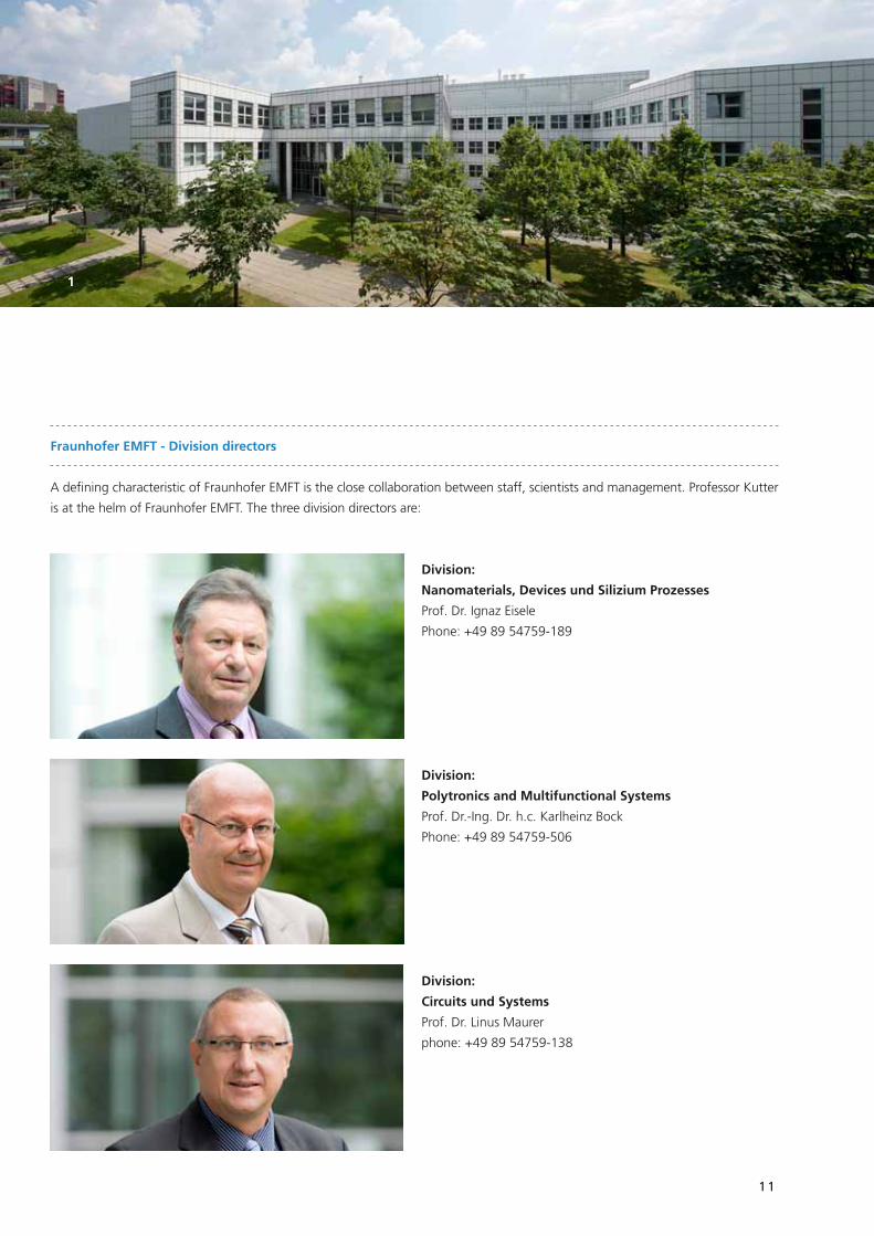
2
Fraunhofer EMFt - division directors
A defining characteristic of Fraunhofer EMFT is the close collaboration between staff, scientists and management. Professor Kutter
is at the helm of Fraunhofer EMFT. The three division directors are:
division:
Nanomaterials, devices und silizium prozesses
Prof. Dr. Ignaz Eisele
Phone: +49 89 54759-189
division:
polytronics and Multifunctional systems
Prof. Dr.-Ing. Dr. h.c. Karlheinz Bock
Phone: +49 89 54759-506
division:
circuits und systems
Prof. Dr. Linus Maurer
phone: +49 89 54759-138
1

12
Operating budget
The Fraunhofer EMFT operating budget continued to develop
positively last year. It amounted to 10,631,000 euros in 2012.
Industrial contracts generated a total volume of just under
2,000,000 euros. The percentage of earned revenue was
therefore approximately 20%. The planned operating budget
for 2013 is EUR 11,266,000, which will involve a further
increase in the institution‘s industrial earnings.
staff development
Fraunhofer EMFT currently employees a staff of 92. Of these,
68 work in the scientific area and another 24 in the areas
of administration, IT and technology. On average there are
over 35 students and research assistants from a wide range
of institutions working on their doctoral thesis, dissertation
or master‘s assignment at Fraunhofer EMFT at any given time
and who are involved in the various research areas.
/ / O V E R V i E w
infrastructure
In the Fraunhofer EMFT building the following infrastructure
exists:
Cleanrooms: (640 m2)
according to DIN EN ISO 14644-1, ISO class 5 (previously 100
US FED standard) and 4 (previously 10 US FED standard)
• 200 mm line with complete range of standard silicon
CMOS equipment
• 150 mm line with complete range of standard silicon
MEMS equipment
Laboratories: (1600 m2)
Polytronics, microfluidics, bioanalytics, ATIS, guest companies
Office areas and meeting rooms: (2760 m2)
• Offices (1520 m2)
• 3 seminar rooms (50 m2, 55 m2 und 80 m2)
• 4 meeting rooms (190 m2)
• 1 video conference room for 15 people (50 m2)
The institution in figures
1 High-grade steel
micropump for application
in medical technology and
biotechnology

13
2
Advisory Board
The Advisory Boards are external consult ing bodies attached to the inst i tutes and research inst i tut ions.
They are made up of representat ives from sc ience, bus iness and publ ic l ife. The approximately twelve
members for each inst i tute are appointed by the Fraunhofer Execut ive Board in agreement with the inst i -
tute management.
At least one member of the Execut ive Board attends the annual meet ings. The Advisory Boards advise the
inst i tut ion management on issues of research or ientat ion and structural change.
The members of the Fraunhofer EMFT Advisory Board are as follows:
• Dr. Hans-Jürgen Bigus, Hirschmann Laborgeräte GmbH & Co. KG
• Dr. Reinhard Fojt, KETEK GmbH
• Prof. Dr. phil. Merith Niehuss, Universität der Bundeswehr München
• Prof. Dr. -Ing. habil. Dr. h. c. mult. Ulrich Rohde, Synergy Microwave Europe GmbH & Co. KG
• Dr. Thomas Scheiter, Siemens AG Corporate Technologies
• Prof. Dr. rer. nat. Doris Schmitt-Landsiedel, Technische Universität München
• Dr. Peter Wawer, Infineon Technologies AG
• Dr. Stefan Wimbauer, Bavarian Ministry for Trade, Infrastructure, Transportation and Technology, Munich
1

14
/ / B U s i N E s s A R E A s
sensor Materials
sensors and Actuators
Microdosage systems
Flexible systems
design and test
1 Sensor glove changes
color as a hazardous
substance warning

15
business AReAs With exAMples oF pRojects
Fraunhofer EMFT organizes i ts research and development programs into f ive business areas. These are
descr ibed below and their act iv i t ies presented based on selected pr ior i ty projects .
1
sensor Materials
Sensor materials are developed at Fraunhofer EMFT which in-
dicate the presence of analyte molecules by means of changes
in color or fluorescence. The materials are based on indicator
dyes and are tailored to the application concerned by means
of integration in polymers, foils, structured surfaces, micropar-
ticles or nanoparticles. For example, sensor particles are used
as nanosensors for analytics in cells. They can also be applied
to surfaces by means of coating or printing techniques.
In the area of textiles, nanosensors can be integrated using the
same techniques as those used for processing the pigments
commonly applied in this field such as screen printing. One
example of a textile application is sensor protective clothing:
if there are toxic or corrosive substances in the ambient air, the
clothing warns the wearer by changing color. Sensor materials
based on a color change to show detection of an analyte can
also be integrated in a range of everyday products. Food
monitoring is highly topical in this connection: here, sensor
packaging which changes color in response to spoilage
processes or high levels of contamination in food is both
highly effective and easy to handle. In the area of fluorescence
analytics, Fraunhofer EMFT develops sensor systems and mo-
dules which can be used in air or water analytics - for instance
by means of integration in measuring devices. In one current
project (ZIM KF2833201ZG1 and E830901ZG1), Fraunhofer
EMFT is collaborating with an industry partner (TriOS Mess-
und Datentechnik GmbH, Rastede) on an O2/CO2-measuring
device based on optical sensors for CO2 and O2. This system
will be designed to simultaneously measure O2/CO2 in water
samples on site in real time. It is based on the development
and combination of new fluorescence indicators to measure
the two analytes and their integration in suitable polymers.
The planned application makes high demands of the sensor
system, including fast response, high sensitivity and not least
a high level of stability and resilience to the impact of trans-
portation and varying storage conditions.
project example: „Hexanal sensor“
The sell-by date on packaging only gives the consumer some
idea of the freshness of the food contained in it. But errors
in packaging, disruptions in the refrigeration chain or leaking
packaging can cause foodstuffs to spoil during distribution or
in households.
Very often it is impossible to detect from the outside that the
food has spoiled or has become inedible or even harmful to
health. So to increase consumer safety, clear indicators would
be useful which show the actual quality of the food.
The „Hexanal Sensor“ project at Fraunhofer EMFT is dedicated
to developing intelligent packaging with color indicator
systems which visibly display the freshness of food products.
The initial aim is to demonstrate the general feasibility of such
indicator systems and create a basis for developing others.
The solution principle is based on the measurement of volatile
aldehydes (e.g. hexanal) in the gaseous phase.
The project specifically involves the creation of an indicator
system which can be visually analyzed to detect oxidative

16
/ / g E s c H ä F t s F E l d E R/ / B U s i N E s s A R E A s
1 CO2- sensor chip on a
circuit board
quality changes - for example in packaged (and opened)
cooking oils and roasted nuts. The aim will then be to inte-
grate this indicator system in packaging foils or in closure
seals for bottles. The developments are of particular relevance
to manufacturers of products containing oil and fat which
spoil as a result of oxidation (e.g. oil mills, the confectionery
industry, manufacturers of baked goods). Additionally, they
are of great interest to end consumers.
The insights gained from this project will also be used as a ba-
sis on which to develop indicator systems for other foodstuffs
(e.g. meat, fish, ready-made products) and will be fed into the
area of sensor technology.
This project is run jointly with Fraunhofer IVV and is sponsored
as internal research geared towards small and medium-sized
companies (project no. 825 352) Concrete project outcomes
are expected in June 2014.
sensors and Actuators
The Sensors and Actuators business area includes the areas of
„Services“ and „Process and component development“.
Services provided include process development and small
series production of silicon-based sensors as well as the
qualification of process media. The aim is to establish close
collaboration with companies and ultimately benefit cus-
tomers: their own staff can make use of Fraunhofer EMFT‘s
cleanroom infrastructure as well as drawing on the expertise
of experienced Fraunhofer EMFT staff.
Small series production at Fraunhofer EMFT makes sense
wherever small volumes are not available on the global
market. A 200 mm CMOS line is available for this purpose,
supplemented by a 150 mm backend line.
Close collaboration also allows typical customer problems
to be solved such as increasing yield and throughput in
small series production. It is possible to jointly analyze the
impact of critical factors on the application so as to enhance
performance. In terms of product development, Fraunhofer
EMFT is currently involved in creating detectors for material
analysis by means of EDX and XRF analysis (Si-drift detector).
Another example is that of single X-ray photon detectors for
medical technology applications which take the form of silicon
photomultipliers and are based on the avalanche diode prin-
ciple. The spectral range can be covered by the properties of
the pure silicon material. For example, Fraunhofer researchers
are developing silicon photomultipliers (SiPM) in 200 mm
technology in collaboration with Ketek GmbH. Initial results
have been highly promising. Ketek GmbH is now seeking

17
to develop the jointly created SiPM to product maturity.
Fraunhofer EMFT is also evaluating use of the components in
other applications such as detection of weak light signals in
the field of analytics.
In the area of process media qualification, customers have the
opportunity to test silicon-based primary substances (gaseous)
or etching and cleaning gases on production-type equipment.
This makes it possible to analyze the purity of supplied
material in the target processes and potentially discover any
extraneous matter which may be present. Any undesirable
impact on production equipment can be tested and proposals
developed for the application. The support from experienced
Fraunhofer EMFT personnel is a key benefit here.
In developing processes and components, the focus is on
components which are distinct from those generally available
on the market due to their special parameters: through-flow
sensors for liquids, low-noise single transistors such as JFETs
and buried-channel HRFETs, gas concentrators and electro-
chemical sensors, just to mention a few. In combination with
device and process simulation and using special processes in
the front-end area of the technology line, concepts for novel
components with improved properties are created which are
adapted to industry specification profiles
1
project example: „components for high-frequency
applications“
The fundamental idea of the MST Bayern project „HRFET - low-
noise field-effect transistors with high-frequency capability“ is to
develop FET transistors which can be used in the GHz range and
are extremely low-noise.
Existing transistor concepts are not capable of meeting both
these specifications. The project is pursuing two concepts: Firstly,
the refinement of so-called JFETs (Junction FETs) - here the
HESDEK project already achieved excellent results in the MHz
frequency range; secondly a new type of CMOS concept with
buried-channel MOS transistors for applications running into the
GHz range.

18
/ / g E s c H ä F t s F E l d E R
Microdosage systems
The handling and dosage of tiny quantities of liquids or gases
is crucial to a wide array of applications nowadays.
Fraunhofer EMFT offers its customers individually tailored
microdosage solutions, giving rise to new products and
applications in the following areas:
• Lubrication dosage
• Laboratory technology
• Medical technology
• Fuel cells
• Micro-cooling systems
• Scent dosage systems
• Analysis systems
For example, microlubrication systems can be used to apply
tiny quantities of lubrication oil (just 5 nanoliters per second)
to a bearing. This can save up to 98% of lubrication oil as
compared to conventional methods of lubrication. In labora-
tory technology, silicon micropumps can replace heavy ceramic
pistons in air displacement pipettes or microtiter plate robots,
making the systems lighter and easier to handle.
The field of medical technology offers a wide range of applica-
tions. One particular area here is medication dosage by means
of externally wearable or implantable systems. The latter can
be used in pain therapy (intrathecal or peridural), for treating
tinnitus (Lidocaine in the middle ear), in hormone therapy
(for treating fertility disorders), tumor therapy (direct dosage
of highly concentrated cytostatics into the tumor tissue) and
in diabetes therapy. There is particularly promising market
potential in the context of insulin treatment for diabetes
patients. All these applications require exact dosage of the
very tiniest amounts. At the same time, the dosage compo-
nents must be disposable and therefore very low-priced.
This is achieved by making microdosage systems out of plastic
or metal. Micropumps can be of valuable assistance in treating
chronic wounds: one example here is the use of innovative
and miniaturized plasters in vacuum therapy. Extremely
miniaturized dosage systems made of silicon are ideal for
implantable applications. For example, micropumps implanted
behind the eye could be used to reduce eye pressure and treat
glaucoma. The same method could help those suffering from
phthisis by preventing them from going blind. Somewhat
larger micropumps made of high-grade steel might replace
the sphincter muscle in the bowel or bladder by means of a
so-called cuff where a saline solution is pumped in (to close it)
or out (to open it).
Analysis systems (e.g. water analysis) use microdosage to
ensure that the analysis sensor is fed with precisely defined
media free of bubbles and particles, enabling exact measure-
ments to be made.
Microdosage technology is an innovative, future-oriented area
but it still poses a number of challenges. These include the
management of bubbles, particles and back pressure, monito-
ring the dosage of minute quantities and chemical resistance.
Fraunhofer EMFT works on all these issues so as to be able to
develop robust products for its customers.
1 Microdosage system
for microlubrication of
precision bearings in high-
performance spindles
/ / B U s i N E s s A R E A s

19
1
Project example: „Piezolub: Self-sufficient,
piezo-powered microdosage component for
lubricants“
Precise lubricant dosage is crucial to ensure smooth-
running production - especially in the case of fully auto-
mated processes: it guarantees a long equipment service
life, prevents premature wear and tear and extends the
maintenance intervals required.
Scientists at Fraunhofer EMFT have developed a new type
of micro-quantity lubricant system in cooperation with Paul
Müller Industrie GmbH & Co KG (GMN). It enables controlled
release of minute quantities of lubricant into precision ball
bearings in high-power spindles. The self-contained dosage
systems with integrated oil reservoir for an anticipated opera-
tional service life of approx. 20,000 hours are designed to be
mounted decentrally on cutter spindles.
Piezoelectrically powered silicon micromembrane pumps are
at the heart of the system, developed at Fraunhofer EMFT and
with a chip size of just 7 x 7 mm2. A new method of dosage
monitoring was also integrated in order to ensure reproducible
oil transport. This is based on a sensor principle for minute
conveyance volumes, likewise developed at Fraunhofer EMFT:
capacitive runtime monitoring of phase boundaries between
oil and air. Another particular area of focus was that of
solutions to avoid free-flow.
GMN supports development work by means of extensive tes-
ting on real machine tool spindles so as to assess the optimum
oil quantity for stable, efficient bearing lubrication. The newly
developed solution based on classic oil/air lubrication offers
several advantages as compared to commercially available
lubricant systems. For example, with dosage units of far less
than 25 μg per second in some cases, only a fraction of the
lubricant is used. In addition to making economic sense,
there is also an ecological bonus. It is also worth mentioning
the health benefit here: after all, it leads to a reduction in
oil contamination of the air in production halls. Less oil in
the bearing also means a lower coefficient of friction, which
in turn increases the efficiency of high-speed spindles.
1

20
/ / B U s i N E s s A R E A s
The Bavarian Polytronic Demonstration Center (BDP) was
established in 2002 for this business unit and in recent years
it has been fitted with state-of-the-art, production-related
equipment for the microfabrication of product demonstrators
on foils. For research projects and development work con-
tracted by industry, the facility now has machines which allow
modular processing of foil sheets or rolls with a width of
210 mm. A microsystems engineering line is also available
which can produce microsystems on a substrate size of
Ø150 mm in a cleanroom. This is used as a standard method
for processing silicon wafers on a service basis, but it is also
well suited to effective prototyping of foil processes under
ideal environmental conditions. Our development work in
the area of flexible systems currently focuses on functional
integration by combining functional materials with related
application-oriented processing. Here the spectrum of integ-
ration options ranges from large-area, flexible wiring systems
based on foil stacks with three-dimensional assembly and
connection structures as well as foil via technologies and the
assembly of optical and sensor components in foil technology
to produce organic printed circuits and systems. In terms of
product development, plastic foils offer a number of benefits
as a large-format substrate material. Firstly, they provide a
large-area, low-cost substrate that enables the creation of fle-
xible, bendable or rollable systems. But the interim stage of a
foil process can also add crucial improvements to non-flexible
applications, for example by thinning power semiconductors
and sensors or by transfer to the heat sink or device surface
by means of foil handling. Foils can also be processed as a
continuous substrate in the form of roll material. This type of
roll-to-roll technique enables highly efficient manufacturing
methods, providing high production volumes especially in
the area of low-cost electronics. A now classic example of
1 Foil-based flexible sen-
sor system used to monitor
various air parameters
Flexible systems
The area of foil systems, or FOLAE (flexible organic and large-
area electronics) has advanced continuously in recent years.
At Fraunhofer EMFT today, various products are developed
and in some cases produced, including sensors, solar cells,
integrated circuits, displays and entire flexible systems. This
has primarily been made possible by technological advan-
cements in the field of functional materials, especially those
based on organic substances (smart materials).
The conductive, semi-conductive, sensoric or luminous pro-
perties of these allow direct integration of the most diverse
components and functions on a wide variety of surfaces by
means of layering techniques. A key focus here is on the
extended pressure technologies and additive coating and
structuring technologies used to create flexible electronic sys-
tems - generally based on the familiar areas of use of printed
media. These techniques enable entirely new functionalities.
Classic electronics can also be integrated on flexible substrates
such as foils or textiles, for example high-performance com-
ponents based on existing wafer technologies such as silicon
CMOS or MEMS.
The relevance of this type of application is obvious: in many
microelectronic products, the trend nowadays is towards
increasingly thin semiconductor elements so as to enhance
performance or facilitate handling. Examples include silicon
chips for power electronics, solar cells, 3D-integrated chip
stacks, micromechanical sensors (MEMS) and also very thin
silicon components as have been used for many years in smart
labels for logistics applications and identification systems. Flat
and flexible multifunctional electronic systems on foil substra-
tes open up a whole new range of potential applications.

21
1
this kind of application is the manufacture of RFID systems in
which aerial coils are printed and fitted with transponder ICs
using a through-feed method.
Roll-to-roll processes have paved the way for new applications
in other areas, too, ranging from electronic paper and rollable
displays to intelligent sensor floors and disposable sensors.
project example: „polyOpto - multifunctional analysis
system for point-of-care applications“
On-site diagnostics in medical technology requires small,
portable and automated devices which can be manufactured
economically and in large numbers.
The project „PolyOpto“ saw Fraunhofer EMFT researchers
developing this kind of multifunctional analysis system,
incorporating electrical, optical and fluidic functionalities on
a plastic foil. Polymer foils as a substrate in combination with
roll-to-roll production techniques ensure material costs are
kept very low.
The individual components for an optical sensor system - light
source, photo transistor and fluid channel - are produced on
foil using layering techniques. The light source used here is an
electroluminescence component. An organic transistor based
on semiconductive TIPS pentacene serves as a light-sensitive
detector. The light source and the detector are produced on
the same foil, so no additional assembly stages are required.
In order to achieve the three-dimensional arrangement of the
sensor system, the foil is folded around a second foil with
fluidic contours. This creates a closed system in which the light
source and phototransistor are placed opposite each other and
are optically linked.
In this way, changes in the optical absorption between the
components can be electrically detected and measured.
Sensor layers can be inserted in the absorption path for this
purpose. In this particular case, laser processing of foils was
used to create a fluid channel enabling the change in optical
absorption to be detected in fluids. Researchers have refined
the system by adding a gas analysis module. For this purpose,
a chromatic gas sensor material was integrated on foil in mo-
dular form together with a pneumatic channel arranged in the
same way made of circular EL lighting and a coaxial pentacene
phototransistor. This allows the concentration of gases to be
determined by reading out color changes in the chromophore
based on the EL lighting and the pentacene phototransistor.
This optoelectronic system largely dispenses with any assembly
of individual components and can be produced by means of
one-sided processing. As mentioned above, roll-to-roll pro-
duction is essentially possible too, increasing manufacturing
efficiency so as to be able to handle large volumes. This type
of low-cost sensor system for one-off use is also of interest
to other areas in addition to medical technology, including
environmental analytics, for example.
This research is funded by the German Federal Ministry of
Education and Research (BMBF) and VDI/VDE Innovation +
Technik GmbH, Project PolyOpto FKZ 16SV3870

22
/ / B U s i N E s s A R E A s
1 CC-TLP electrode via
wafer (raised)
design and test
With its business unit „Design and Test“, Fraunhofer EMFT
offers its customers individually tailored solutions, ranging
from system design through to reliability assessment.
The services offered are as follows:
• Design of complete systems as devices, subsystems and
integrated components
• Multiparametric characterization of systems and
components
• Reliability prognoses with regard to the planned
application
Thereby commercially available technologies are used, as well
as technologies produced by Fraunhofer EMFT and adapted to
customers‘ specific needs. The leitmotif in this business area is
the duality of simulation and experiment.
The current focus area in design development is in the field of
microprocessor-controlled systems which use sensors to
capture, process, store specific parameters and/or ultimately
trigger actuators. One example of this is the microfluidic
systems including micropumps and microvalves which are
controlled by means of sensor measurement technology.
The design of integrated components, cells and circuits with
low integration density is currently being developed: here
Fraunhofer EMFT is focusing on the areas of analog and high
frequency. Using multiparametric characterization, it is
possible to simulate physical input variables such as voltage,
current, temperature, light, moisture, gases etc. under
laboratory conditions and compare the reaction of the
component to the variable on its own as well as collectively.
The results provide a basis for assessing measurement
precision and reproducibility. By means of appropriate load
tests which address success-related error mechanisms, it is
also possible to apply these methods to determine expected
reliability and lifetime. The range of services finally includes
systematic analysis of the causes of complex errors and relia-
bility problems in electronic components and systems as well
as their reproduction under laboratory conditions, including
identification of falsifications.
As mentioned above, Fraunhofer EMFT has its own in-house
developments which usefully complement commercially
available equipment.
One example of such a specialized system is the M-CDM ESD
tester. It is now also used directly by industry with specially ad-
apted software. The M-CDM ESD extension CC-TLP Capacitive
Coupled Transmission Line Pulsing and a bending machine for
flexible substrates have similar potential.

23
11
project example: „i-tex“
The FP7 project i-Tex „Intelligent and luminous textiles“
(www.i-tex.nl) researches and develops energy-efficient,
large-area lighting systems based on inorganic light-emitting
diodes (LED). As part of this project, Fraunhofer EMFT Working
Group ATIS runs the work package „Characterization and
Reliability“.
Since the lighting systems are initially to be used in architec-
ture and high-quality tents, there is particular focus on relia-
bility as well as the functional, technical aspects and aesthetic
properties of the lighting.
In addition to visual properties, investigation is carried out
into the conductivity of the electrical connections, insulation
between the conductors and the impact of temperature and
moisture, as well as tensile and flexural stress.
Particular importance is attached to electrostatic discharge
(ESD): after all, without the appropriate protective measures,
the load-sensitive LEDs would be exposed to dangerously high
levels of static voltage of many kilovolts even while being
woven into the textiles and during roll-to-roll coating.
As part of its i-Tex activities, the working group develops
methods and test devices for multiparametric electrical,
thermal and optical characterization and flexural stress. It also
produces computer-controlled, analyzable sensors for room
and lighting parameters as well as power sources to supply
test vehicles and demonstrators.

24
/ / c O R E c O M p E t E N c E s
1 Smart pigments
Functional Molecules
and surfaces
silicon processes, device
and 3d integration
Heterointegration and
Foil technologies
systems und
prototypes
sen
sor
Mat
eria
ls
sen
sors
an
d
Act
uat
ors
Mic
rod
osa
ge
syst
ems
Flex
ible
sys
tem
s
des
ign
an
d t
est

25
Functional Molecules and surfaces
Fraunhofer EMFT possesses outstanding expertise in the selec-
tive synthesis of indicator dyes, in handling polymer systems
and in the creation of functional polymers and surfaces by
means of chemical modifications.
The knowhow in this area has produced a wide range of
application-related demonstrators such as optical sensor foils.
The production of responsive optical materials starts with
the selective synthesis of suitable indicator molecules for
fluorescence or absorption tests. The applications are stably
immobilized on surfaces so as to be able to adapt the indica-
tors to them.
This is carried out by embedding them in polymers (smart
dyes) or by bonding them to the surfaces of microparticles or
nanoparticles (smart pigments). Where such sensor particles
are synthetically structured, core-shell systems can be used to
combine multiple functions and generate properties such as
hydrophilicity, hydrophobia or polarity.
Optical sensor foils
Sensor foils can be used in a variety of different ways, in the
form of test strips in medical diagnostics, biotechnology,
environmental analytics and process characterization, for
example. They are likewise used in product authentication
by installing fluorescent indicators.
Sensor materials also have enormous potential in the textile
industry. Foil strips for integration in textiles (e.g. protective
oveRvieW oF coRe coMpetences
Fraunhofer inst i tutes offer se lected core competences a imed at tackl ing future technological chal lenges
fac ing society, bus iness and industry. Fraunhofer EMFT groups i ts areas of research and development ex -
pert ise into four core competence areas. These are descr ibed below.
1
gloves, laboratory clothing or protective suits) can change
color to indicate toxic substances in the environment or con-
tamination by aggressive chemicals.
In the area of food monitoring, sensor foils integrated in
packaging can determine and display the freshness of the con-
tents. This makes it possible to reliably identify the quality and
freshness of food (such as meat and fish products) - a simple
and effective method from which all those involved can bene-
fit - from the retail chain through to the end consumer.
Surfaces on vehicles and machines can also be coated with
sensor materials, allowing 3D imaging of physical parameters
such as pressure and temperature.
In addition to indicator modules, Fraunhofer EMFT also deve-
lops a range of optical measurement modules (e.g. incident
light module, fluorescence module) and adapts them to the
various properties of the sensor materials. In addition to detec-
ting optical signals, these modules also enable measuring data
to be stored and transmitted.

26
/ / c O R E c O M p E t E N c E s
1 Photodetector system
for sensoric lab-on-chip
applications integrated
by means of layering
technology
silicon processes, device and 3d integration
In addition to CMOS technology, this core competence breaks
down into the following areas of work:
• 3D integration / MEMS technology
• Thin wafer technology
• Epitaxy
A key feature of 3D integration by means of through-platings
through the silicon of a circuit (through silicon vias, TSV) is the
combination of tungsten vias with the structuring of sub-
systems based on intermetallic connections made of copper
and tin. The various electrical circuits are generally produced,
tested and supplied externally at wafer level, independently
of one another. At Fraunhofer EMFT they are then vertically
integrated by means of standard CMOS-compatible slice pro-
duction processes in a 3D subsystem (wafer level 3D system
integration). The flexibility of the technologies allows solutions
to be created which are specifically tailored to customer needs.
The following process modules are available:
• Structuring of silicon by means of STS TS Bosch etching
process
• Electrical through-plating based on tungsten CVD
• Low temperature processes on thinned wafers
• Solid liquid interdiffusion of Cu/Sn to assemble subsys-
tems (SLID bond)
MEMS technology is based on subsequent process modules
for the removal of oxides without adhesion of free-moving
MEMS structures.
• VS-RS proximity lithography (150, 200 mm)
• Wafer fusion bond (SFB)
• Electroplating for copper and tin (100, 150, 200 mm)
• Wet chemical Si structuring with KOH (150 mm)
• Release etching with HF steam (150 mm)
The combination of special processes offers an extensive
range of technological options - from flexible solutions
through to small wafer quantities. Another particular fea-
ture is the process sequence to SFB from structured silicon
wafers, allowing for complex MEMS components.
Technologies for the production of thin wafers are directly
linked to 3D integration. Here Fraunhofer EMFT is able to
supply any type of thin device at wafer level, drawing on
years of experience and expertise (also documented in the
relevant patents). Fraunhofer EMFT is excellently equipped to
carry out the relatively elaborate process sequence of thinning
technology: it has two grinders for fast material removal, a
spin etcher for wet chemical removal of strains, two systems
for polishing processes (CMP; chemical mechanical polishing)
as well as optical and capacitive thickness measurement to
monitor thinning results. Wafer cleaners are available for
cleaning purposes for use in follow-up processes.
The selection of processes for wafer thinning is based on
insights gained from material analytics and the flexure and
fracture response of thinned semiconductor substrates,
as developed at Fraunhofer EMFT over many years.
Fraunhofer EMFT offers the patented „dicing by
thinning“ method as a chip separation technique for
very thin semiconductor wafers: this allows efficient
manufacture of individual ultrathin chips with optimum

27
flexural strength. These techniques permit the production
of silicon chips with a thickness of 10 μm - 30 μm.
The required distribution of the wafers in chips is carried
out by means of dry etching systems which use the Bosch
process for high-rate silicon etching.
Other focus areas are silicon epitaxy for high-impedance,
intrinsic layers and SiGe epitaxy for selectively strained
layers or sacrificial layers. Combining Si and SiGe epitaxy
it is possible to make new components for microsystems
engineering such as NEMS (Nano Electro Mechanical Systems
with nanogaps). A low-temperature epitaxy system for
silicon and SiGe is currently being established as a consistent
refinement of the core competence. Depositions are to be
carried out at temperatures as low as - 450 °C, thereby
allowing further handling of ready-processed CMOS circuits.
Heterointegration and Foil technologies
With its laboratory facilities and technological experience in
the area of polytronic technologies - especially roll-to-roll ma-
nufacturing technology for foil systems - Fraunhofer EMFT has
at its disposal a unique technology platform for the develop-
ment of multifunctional electronic systems. One area of focus
here is heterointegration: the merging of distinct technological
worlds paves the way for new, effective solutions to produce
components and systems and to integrate systems in flexible
substrates. Fraunhofer EMFT combines developed print tech-
nologies with technologies and processes from various con-
ventional technological fields (e.g. silicon, MEMS or circuit
board technology). These technologies can be diversified and
supplemented as needed. What is more, the interfaces bet-
ween the technologies can be adapted to the application in
question. The processes can also be transferred to large-area
and large-volume production procedures for system integ-
ration and for product manufacture on flexible substrates.
Mobile electrostatic carrier
With its patented concept of the mobile electrostatic carrier,
Fraunhofer EMFT offers a technical solution which enables
simple and secure handling of very thin semiconductor wafers.
These so-called e-carriers draw on electrostatic forces to rever-
sibly fix a fragile circuit substrate. The carrier itself consists of
a silicon wafer of which the electrode surfaces on the front
can be electrically charged and discharged by means of
through silicon via (TSV) technology using the contact surfaces
on the back. In 2011 these carriers with bipolar electrode con-
figuration were also applied to silicon wafers with a diameter
of 200 mm for the first time.
1
28
/ / c O R E c O M p E t E N c E s
Multilayer and through-plating processes
Fraunhofer EMFT has many years of experience in the produc-
tion of high-density wiring systems on foils with conductor
path grids of 30 µm and less. These enable direct chip integra-
tion. However, several conduct path systems usually have to be
applied to achieve an efficient layout and increased packaging
densities. These are obtained either by means of a multilayer
structure on one substrate side or by using the back of the foil
for double-sided wiring for the latter. A process technique has
been developed at Fraunhofer EMFT which allows continuous
manufacture using the roll-to-roll method. Here a via bore is
carried out using a combination of laser processing and plas-
ma etching. Other key stages here are electroplating processes
to create a number of copper conductor paths several µm
thick as well as wall metallization of the through-platings.
Organic electronics
Organic semiconductors are regarded as the material of
the future for the production of electronics with additional
function since they can be handled using efficient plastics
engineering processes. Over a period of more than ten years,
Fraunhofer EMFT has acquired broad expertise in roll-to-roll
manufacturing - for example of contactless smart sensor
applications or complementary organic electronics applied
directly to foil substrates.
The institution‘s extensive expertise includes specially deve-
loped process stages used to advance the miniaturization of
organic components in the µm and sub-µm range; for ex-
ample, Fraunhofer EMFT is involved with transistors in this
area. For this purpose, novel structuring techniques such as
nanoimprinting and microcontact printing have been deve-
loped, as well as processes for the deposition of ultrathin
polymer dielectric layers on roll substrates.
When scaling transistor geometry down to smaller dimensions,
particular importance is attached to the dielectric medium for
gate insulation. In view of the increasingly thin layers, error-
free electrical insulation and a high voltage rating has to be
ensured. At Fraunhofer EMFT it is already possible to produce
layers with a thickness of just 200 nm and an extremely high
level of dielectric strength. Increasing miniaturization is a key
requirement in order to further raise the switching frequencies
of organic transistors, for example, which are currently at
100 kHz.
These issues were investigated as part of the EU-sponsored
projects INTERFLEX (ICT 247710), COSMIC (ICT 247681) and
POLARIC (ICT 247978).
1 „TUDOS“ microdosage
system for dosage of cytos-
tatics in tumor therapy

29
systems and prototypes
This core competence includes the subareas of system
development as well as the analysis and testing of systems.
Development expertise includes hardware and software,
electronics, mechanics, optics and fluidics with micropumps
and microvalves. It is based on the longstanding experience
of Fraunhofer EMFT staff in the development of complex
systems. Services provided by Fraunhofer EMFT in the field of
system development range from the initial concept through
to feasibility demonstrators and prototypes, according to
needs. Both microcontrollers and PCs are used for control
purposes.
In the area of analysis and testing, Fraunhofer EMFT has a
wealth of experience in investigating the causes of complex
errors and reliability problems in electronic components. The
institution has developed solutions for ESD and other reliability
tests for over 20 years, either under contract to customers or
in the context of joint projects.
Fraunhofer EMFT experts are able to support customers with
special methods of analysis, specialized equipment and ser-
vices to identify error causes and to harden technologies. The
expertise portfolio also includes multiparametric characteri-
zation on the wafer or in the system. Among other things,
high current pulses are generated with ps rise times and
measured with a single-shot bandwidth of up to 50 GHz.
The main application of this technology is the development
of high-performance ESD protection concepts based on
integrated, discreet protective elements. These devices can
also be used to determine system responses directly in time
domain to individual events which are difficult to reproduce.
CW high-frequency measuring technology can penetrate the
lower mm wave range with up to 110 GHz and is supple-
mented with field and circuit simulations using Agilent ADS.
Finding the causes of complex errors and reliability problems
in electronic components requires many years of experience
with the various development and manufacturing processes
throughout the entire supply chain as well as the stress
profiles occurring in the application.
The expertise of Fraunhofer EMFT staff also provides a
valuable basis for successful robustness validation as has
been established in automotive electronics.
1

30
/ / R E s E A R c H F i E l d s A N d s E R V i c E s
1 Chips on wafer connec-
ted by means of flip chips
2 Fraunhofer scientist in
the laboratory at the FCB3
bonder
1
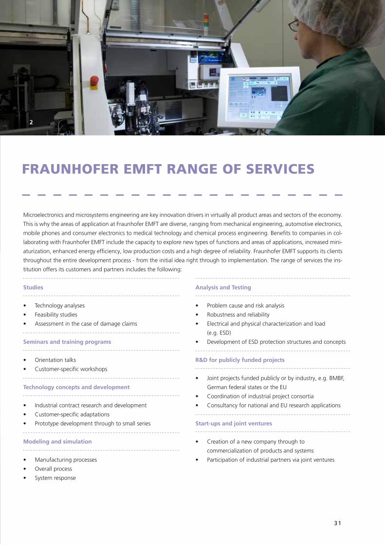
31
FRAunhoFeR eMFt RAnge oF seRvices
studies
• Technology analyses
• Feasibility studies
• Assessment in the case of damage claims
seminars and training programs
• Orientation talks
• Customer-specific workshops
technology concepts and development
• Industrial contract research and development
• Customer-specific adaptations
• Prototype development through to small series
Modeling and simulation
• Manufacturing processes
• Overall process
• System response
Analysis and testing
• Problem cause and risk analysis
• Robustness and reliability
• Electrical and physical characterization and load
(e.g. ESD)
• Development of ESD protection structures and concepts
R&d for publicly funded projects
• Joint projects funded publicly or by industry, e.g. BMBF,
German federal states or the EU
• Coordination of industrial project consortia
• Consultancy for national and EU research applications
start-ups and joint ventures
• Creation of a new company through to
commercialization of products and systems
• Participation of industrial partners via joint ventures
Microelectronics and microsystems engineering are key innovation drivers in virtually all product areas and sectors of the economy.
This is why the areas of application at Fraunhofer EMFT are diverse, ranging from mechanical engineering, automotive electronics,
mobile phones and consumer electronics to medical technology and chemical process engineering. Benefits to companies in col-
laborating with Fraunhofer EMFT include the capacity to explore new types of functions and areas of applications, increased mini-
aturization, enhanced energy efficiency, low production costs and a high degree of reliability. Fraunhofer EMFT supports its clients
throughout the entire development process - from the initial idea right through to implementation. The range of services the ins-
titution offers its customers and partners includes the following:
2

32
/ / R E s E A R c H F i E l d s A N d s E R V i c E s
Cutt ing-edge infrastructure, a broad range of technologies and wel l -developed network of partners in
industry as wel l as among research inst i tutes (univers i t ies ) and publ ic author i t ies make Fraunhofer EMFT
an attract ive partner in research and development, of interest to smal l and medium-s ized companies as
wel l as larger-scale industr ia l enterpr ises. Market ing the results of research is general ly the responsibi l i ty
of the corporate partner. S ince 2007, Fraunhofer EMFT has a lso offered high-tech companies the oppor-
tunity to hire and ut i l ize i ts h igh-qual i ty fac i l i t ies (such as c leanrooms, laborator ies, workshops and
equipment) . Several companies have entered into strategic cooperat ion with Fraunhofer EMFT - inc luding
Siemens AG, Ketek GmbH, Panasonic, Süss MicroTec GmbH, Thin Mater ia ls and TÜV Süd. Framework con -
t racts are being prepared with a number of others companies. Here is a se lect ion of the technological
fac i l i t ies avai lable at Fraunhofer EMFT:
200 mm cMOs technology
• Wet chemical cleaning and etching processes
• Photolithography
• Epitaxy (Si, SiGe)
• Ion implantation and annealing
• Dielectric layers (thermic oxidation, LPCVD deposition of
SiO2 and Si3N4, PECVD of SiO2 and Si3N4)
• Highly conductive layers (Al/Si, Ti, W, doped poly-Si)
• Plasma etching processes (Si, SiO2, Si3N4, Al, W)
• Electroplating (Cu, Sn)
200 mm lithography cluster
• Proximity exposure
• Double-sided exposure
• Contact exposure
• Electron ray exposure
• Ion ray exposure
• i-line stepper
• Nanoimprint
1 Fraunhofer EMFT
scientist at simulation
system
FRAunhoFeR eMFt RAnge oF technologies
si-MEMs technology
• Cleanroom technology for 150mm wafers (silicon,
ceramics, glass)
• Metal coating (Cu, Ti, TiW, Pt, Au, Ni)
• Dielectric layers (SiO2, Si3N4, SiC, PI)
• Wafer bonding, bonding techniques by means of
adhesion
• Structuring with mask aligner 2 μm
Analytics and material characterization
• Atomic force microscope (AFM): measurements of surface
roughness and step measurements up to max. 6 μm
• In-line REM (Schottky emitter) and focused ion beam
(Ga-FIB) with EDX and gas injection system (GIS)
• Spectral ellipsometer: measurement of thin layers and
transparent materials
• Spectrometer: measurement of layer thickness of silicon
(thick layers) and infrared permeable layers
• Target grinding device for sample preparation (grinding
accuracy: ±2 μm)
33
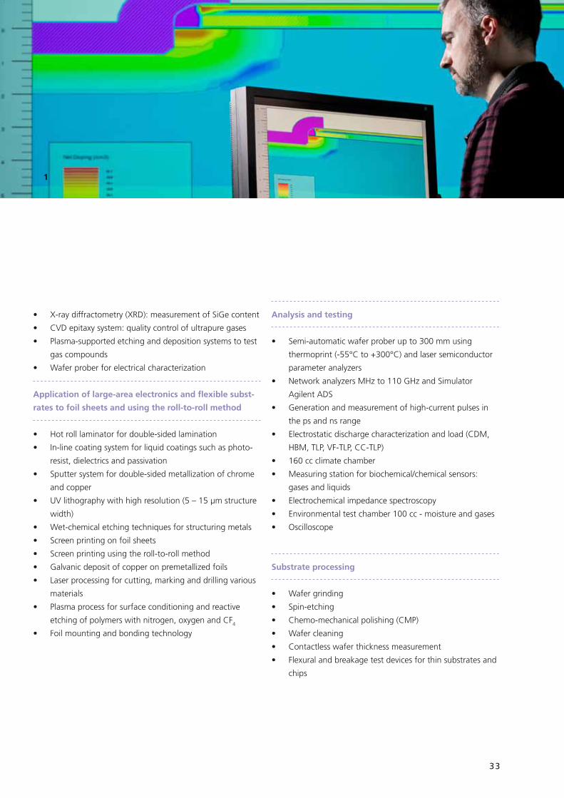
Analysis and testing
• Semi-automatic wafer prober up to 300 mm using
thermoprint (-55°C to +300°C) and laser semiconductor
parameter analyzers
• Network analyzers MHz to 110 GHz and Simulator
Agilent ADS
• Generation and measurement of high-current pulses in
the ps and ns range
• Electrostatic discharge characterization and load (CDM,
HBM, TLP, VF-TLP, CC-TLP)
• 160 cc climate chamber
• Measuring station for biochemical/chemical sensors:
gases and liquids
• Electrochemical impedance spectroscopy
• Environmental test chamber 100 cc - moisture and gases
• Oscilloscope
substrate processing
• Wafer grinding
• Spin-etching
• Chemo-mechanical polishing (CMP)
• Wafer cleaning
• Contactless wafer thickness measurement
• Flexural and breakage test devices for thin substrates and
chips
11
• X-ray diffractometry (XRD): measurement of SiGe content
• CVD epitaxy system: quality control of ultrapure gases
• Plasma-supported etching and deposition systems to test
gas compounds
• Wafer prober for electrical characterization
Application of large-area electronics and flexible subst-
rates to foil sheets and using the roll-to-roll method
• Hot roll laminator for double-sided lamination
• In-line coating system for liquid coatings such as photo-
resist, dielectrics and passivation
• Sputter system for double-sided metallization of chrome
and copper
• UV lithography with high resolution (5 – 15 µm structure
width)
• Wet-chemical etching techniques for structuring metals
• Screen printing on foil sheets
• Screen printing using the roll-to-roll method
• Galvanic deposit of copper on premetallized foils
• Laser processing for cutting, marking and drilling various
materials
• Plasma process for surface conditioning and reactive
etching of polymers with nitrogen, oxygen and CF4
• Foil mounting and bonding technology

34
-
/ / c U s t O M E R s A N c O O p E R A t i O N p A R t N E R s
1
1 Fraunhofer scientist
holding glass wafer
2 MOTT logo

35
-
technology netWoRks
In order to enable eff ic ient and effect ive col laborat ion with industry and develop product ideas into con-
crete appl icat ions more swift ly , Fraunhofer EMFT has establ ished three technology networks for specif ic
themes and research areas. These are a imed at longstanding customers and development partners as wel l
as new customers who wish to draw on expert support to implement their innovat ive product ideas.
Multifunctional On-top technologies (MOtt)
The development center for multifunctional on-top technolo-
gies (MOTT) for standard silicon and CMOS was founded in
2009. Building on the results of previous research into CMOS
circuits and 3D-integration, the Munich site offers a techno-
logy platform for microsystems and nanosystems engineering
which is designed to enable industry to carry out rapid system
development closely geared towards end products.
The platform supports modular integration of new functions
and components in existing silicon standard technologies, re-
sulting in cost-effective solutions even for small and medium-
sized companies.
center for Microsystem integration Munich (cMM)
Together with leading Bavarian companies, Fraunhofer EMFT
initiated the founding of the Center for Microsystem Inte-
gration Munich (CMM) in 2010.
Pooling of the extensive expertise of prestigious partners in
the field of technology and product development makes the
CMM a high-performance, efficient technology network in
the field of microsystems engineering. The CMM acts as the
nucleus for a microsystems engineering center and is looking
forward to further expansion as it is joined by further experts.
Bavarian polytronic demonstration center (Bdp)
Providing a networked environment geared towards human
needs (Ambient Assisted Living, AAL) requires cost-effective,
multifunctional, ubiquitous systems. In order to establish the
infrastructures needed for this purpose, electronic systems
have to be produced economically in large volumes on large-
area substrates.
The Bavarian Polytronic Demonstration Center is a technology
cluster which enables development of the necessary produc-
tion processes, including low-cost microsystems.
A large number of coating and structuring processes for
foils are developed in collaboration with industry focusing
on research projects and development activities for flexible,
organic and large-area electronics (FOLAE). The equipment
used is consistently designed to process rolls of foil.
Current focus areas are functional integration via active orga-
nic materials, the assembly of sensors in polymer technology
and the creation of large-area, flexible wiring systems.
2

36
inDustRy AnD pRoject pARtneRs
The success of Fraunhofer EMFT is founded upon strong industry and project partners and an above-
average level of customer sat isfact ion.*
/ / c U s t O M E R s A N d c O O p E R A t i O N p A R t N E R s
1 Fraunhofer EMFT
scientist at the wafer pro-
ber measuring station
37
1
* This double page shows the logos of some of our project partners. If you are a customer and you do not see your logo here but would like to be
included in the next annual report, please let us know!
38
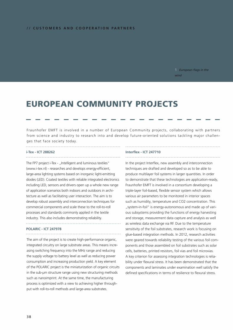
euRopeAn coMMunity pRojects
i-Tex - ICT 288262
The FP7 project i-Tex - „Intelligent and luminous textiles“
(www.i-tex.nl) - researches and develops energy-efficient,
large-area lighting systems based on inorganic light-emitting
diodes (LED). Coated textiles with reliable integrated electronics
including LED, sensors and drivers open up a whole new range
of application scenarios both indoors and outdoors in archi-
tecture as well as facilitating user interaction. The aim is to
develop robust assembly and interconnection techniques for
commercial components and scale these to the roll-to-roll
processes and standards commonly applied in the textile
industry. This also includes demonstrating reliability.
POLARIC - ICT 247978
The aim of the project is to create high-performance organic,
integrated circuitry on large substrate areas. This means incre-
asing switching frequency into the MHz range and reducing
the supply voltage to battery level as well as reducing power
consumption and increasing production yield. A key element
of the POLARIC project is the miniaturization of organic circuits
in the sub-µm structure range using new structuring methods
such as nanoimprint. At the same time, the manufacturing
process is optimized with a view to achieving higher through-
put with roll-to-roll methods and large-area substrates.
/ / c U s t O M E R s A N d c O O p E R A t i O N p A R t N E R s
Fraunhofer EMFT is involved in a number of European Community projects , col laborat ing with partners
f rom sc ience and industry to research into and develop future-or iented solut ions tackl ing major chal len-
ges that face society today.
Interflex - ICT 247710
In the project Interflex, new assembly and interconnection
techniques are drafted and developed so as to be able to
produce multilayer foil systems in larger quantities. In order
to demonstrate that these technologies are application-ready,
Fraunhofer EMFT is involved in a consortium developing a
triple-layer foil-based, flexible sensor system which allows
various air parameters to be monitored in interior spaces
such as humidity, temperature and CO2 concentration. This
„system-in-foil“ is energy-autonomous and made up of vari-
ous subsystems providing the functions of energy harvesting
and storage, measurement data capture and analysis as well
as wireless data exchange via RF. Due to the temperature
sensitivity of the foil substrates, research work is focusing on
glue-based integration methods. In 2012, research activities
were geared towards reliability testing of the various foil com-
ponents and those assembled on foil substrates such as solar
cells, batteries, printed resistors, foil vias and foil microvias.
A key criterion for assessing integration technologies is relia-
bility under flexural stress. It has been demonstrated that the
components and laminates under examination well satisfy the
defined specifications in terms of resilience to flexural stress.
1 European flags in the
wind

39
COLAE - ICT 288881
Commercialization Clusters of OLAE (Organic and Large Area
Electronics) (COLAE) is a European initiative which promotes
the commercial use of organic and large-area electronics.
OLAE technology provides opportunities for new product
ideas, combined with low-cost manufacture, energy-efficiency
and environment-friendly materials and processes. Since this
is a young technology, there are currently very few companies
in Europe who are active in this field and working on product
development. COLAE therefore aims to raise the profile of
OLAE among potential end users in Europe and point the
way forward to innovative product developments. In order to
achieve this aim, demonstrators are developed and training
programs organized for potential industrial clients. COLAE
also seeks to open up new areas of application for OLAE as
well as identifying the main needs and challenges relating to
research and development.
COSMIC - ICT 247681
The project COSMIC has set itself the aim of developing the
electrical properties of organic thin-film transistors to achieve a
performance range required for application in ID tags, display
drivers or other integrated circuits. A key element of the project
is the development of a complementary and significantly more
robust circuit technology with p-type and n-type conductive
organic materials. Development is carried out on various pro-
duction platforms so as to cover the different fields - from
applications with a high degree of integration density through
to low-cost mass products. The results of the project can be
deployed in a diverse range of application areas such as medical
technology, environment, energy, leisure, security and mobility.
NanoMend - ICT 280581
The project NanoMend is dedicated to the development of
new technologies to reduce microdefects and nanodefects
on thin, coated, large-area foil substrates. Surface defects
can arise in various phases of the manufacturing process and
have a negative impact on the efficiency and yield of the
process as well as on the quality and lifetime of the products.
Conventional methods are not able to detect and repair such
defects on a micrometer and nanometer scale. For this reason,
the project focuses on identifying and characterizing as well as
eliminating and repairing this type of defects. These are used
in manufacturing such items as flexible illuminants, flexible
voltaics, coated packaging materials, billboards and screens.
SMART-EC - ICT 258203
The aim of the SMART-EC project is to develop energy-autono-
mous (EC) components. For this purpose, thin foil-based EC
transistors are integrated on flexible substrates with functio-
nalities for energy harvesting and storage. The primary goal
is to improve the energy efficiency of the components so as
to make the applications more convenient and reliable. The
results of the project can be used in such areas as automotive,
ID cards and smart packaging. On this project, Fraunhofer
EMFT is developing assembly methods for foil subsystems on
foil substrates. The aim will be automation using a pick-and-
place machine and optical quality control. A new method is
also being investigated to integrate ICs on foil.
1
40
/ / c U s t O M E R s A N d c O O p E R A t i O N p A R t N E R s
e-BRAINS - ICT 257488
The Fraunhofer EMFT is involved in the large-scale integrated
project e-BRAINS, funded by the European Commission.
e-BRAINS stands for „Best-Reliable Ambient Intelligent Nano-
sensor Systems by Heterogeneous Integration“.
The aim is to provide technologies for future applications in
the field of Ambient Assisted Living which require integration
of heterogeneous technologies. One of the main tasks here is
to develop suitable and reliable 3D integration technologies
for future MEMS/IC products. The e-BRAINS project also
involves selective evaluation of medical (DNA sensors and
active implants) and safety applications. The project partners
are Infineon Technologies (Project Coordinator), eesy-ID, ELA
Medical, IQE, Magna Diagnostics, SensoNor, Siemens, Vermon,
DMSC (majority owned by Intel Mobile Communications),
CEA, EPFL, IMEC, ITE, SINTEF, TUC, TUG, Fraunhofer IIS-EAS
and Fraunhofer EMFT (Technical Manager).
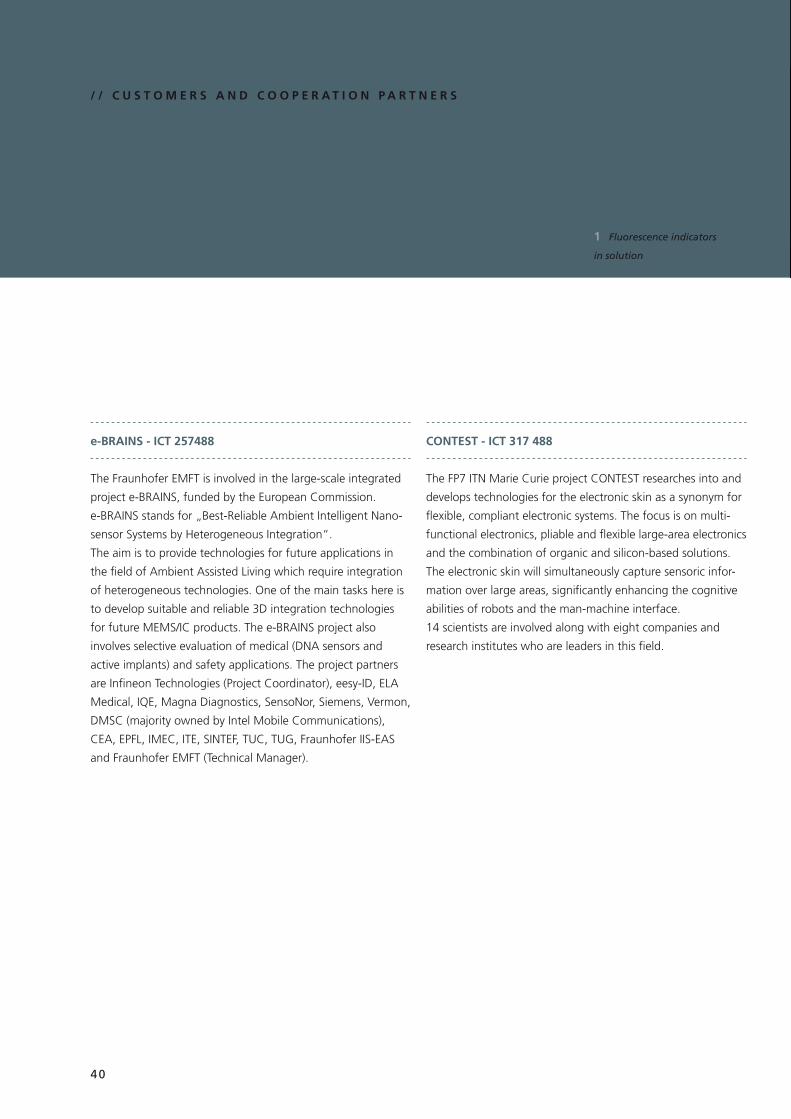
1 Fluorescence indicators
in solution
CONTEST - ICT 317 488
The FP7 ITN Marie Curie project CONTEST researches into and
develops technologies for the electronic skin as a synonym for
flexible, compliant electronic systems. The focus is on multi-
functional electronics, pliable and flexible large-area electronics
and the combination of organic and silicon-based solutions.
The electronic skin will simultaneously capture sensoric infor-
mation over large areas, significantly enhancing the cognitive
abilities of robots and the man-machine interface.
14 scientists are involved along with eight companies and
research institutes who are leaders in this field.
41
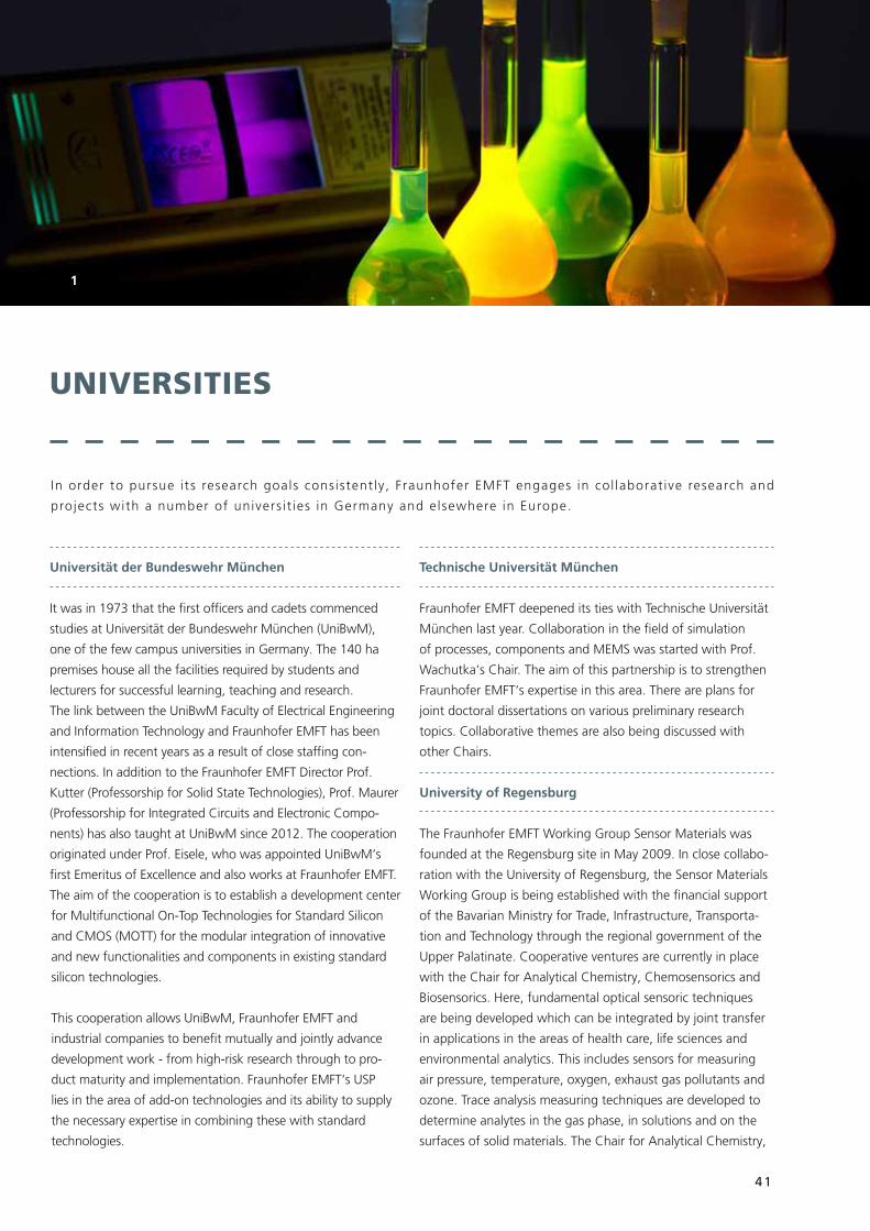
univeRsities
In order to pursue i ts research goals consistent ly , Fraunhofer EMFT engages in col laborat ive research and
projects with a number of univers i t ies in Germany and elsewhere in Europe.
Universität der Bundeswehr München
It was in 1973 that the first officers and cadets commenced
studies at Universität der Bundeswehr München (UniBwM),
one of the few campus universities in Germany. The 140 ha
premises house all the facilities required by students and
lecturers for successful learning, teaching and research.
The link between the UniBwM Faculty of Electrical Engineering
and Information Technology and Fraunhofer EMFT has been
intensified in recent years as a result of close staffing con-
nections. In addition to the Fraunhofer EMFT Director Prof.
Kutter (Professorship for Solid State Technologies), Prof. Maurer
(Professorship for Integrated Circuits and Electronic Compo-
nents) has also taught at UniBwM since 2012. The cooperation
originated under Prof. Eisele, who was appointed UniBwM‘s
first Emeritus of Excellence and also works at Fraunhofer EMFT.
The aim of the cooperation is to establish a development center
for Multifunctional On-Top Technologies for Standard Silicon
and CMOS (MOTT) for the modular integration of innovative
and new functionalities and components in existing standard
silicon technologies.
This cooperation allows UniBwM, Fraunhofer EMFT and
industrial companies to benefit mutually and jointly advance
development work - from high-risk research through to pro-
duct maturity and implementation. Fraunhofer EMFT‘s USP
lies in the area of add-on technologies and its ability to supply
the necessary expertise in combining these with standard
technologies.
technische Universität München
Fraunhofer EMFT deepened its ties with Technische Universität
München last year. Collaboration in the field of simulation
of processes, components and MEMS was started with Prof.
Wachutka‘s Chair. The aim of this partnership is to strengthen
Fraunhofer EMFT‘s expertise in this area. There are plans for
joint doctoral dissertations on various preliminary research
topics. Collaborative themes are also being discussed with
other Chairs.
University of Regensburg
The Fraunhofer EMFT Working Group Sensor Materials was
founded at the Regensburg site in May 2009. In close collabo-
ration with the University of Regensburg, the Sensor Materials
Working Group is being established with the financial support
of the Bavarian Ministry for Trade, Infrastructure, Transporta-
tion and Technology through the regional government of the
Upper Palatinate. Cooperative ventures are currently in place
with the Chair for Analytical Chemistry, Chemosensorics and
Biosensorics. Here, fundamental optical sensoric techniques
are being developed which can be integrated by joint transfer
in applications in the areas of health care, life sciences and
environmental analytics. This includes sensors for measuring
air pressure, temperature, oxygen, exhaust gas pollutants and
ozone. Trace analysis measuring techniques are developed to
determine analytes in the gas phase, in solutions and on the
surfaces of solid materials. The Chair for Analytical Chemistry,
1

42
/ / c U s t O M E R s A N d c O O p E R A t i O N p A R t N E R s
Chemosensorics and Biosensorics also possesses considerable
expertise in the field of biosensorics using physical transducers
such as plasmon resonance (SPR) and impedimetry.
The cooperation between the Sensor Materials Working
Group and the University of Regensburg is constantly
expanded through joint acquisition of sponsored projects,
participation in lectures and joint support for students.
Other research topics are in the areas of adhesion, inter-
diffusion barriers, electrical contacting of polymers and the
self-arrangement and selective electronic alignment of semi-
conductive polymers. The more stable and more efficient layer
systems thereby created serve to enhance the stability and
reliability of the components of which they form a part - after
all, many problems of reliability can be traced back to uncont-
rolled or impaired boundary layers.
technische Universität Berlin
Technische Universität Berlin and Fraunhofer EMFT are linked
by the Professorship for Polytronic Microsystems under
Professor Karlheinz Bock. The aim in this area is to conduct
research into the workings of polytronic components and sys-
tems. Polytronic microsystems are made up either partially or
wholly of active and passive organic materials for conductor,
semiconductor and functional layers (heterointegrated plastic
microsystems). This department is dedicated to research
into polymers, mainly low-cost coating technologies and
the characterization and control of polymeric surfaces and
boundary layers in polymeric material composites as well as
in hybrid multilayer technologies. Increased mobility of the
semiconductive polymer layers is of key importance here
and can be achieved by improving the short-range order
of semiconductive molecules. This can be brought about by
applying technological methods to influence surface states,
e.g. microstructuring and nanostructuring of the technological
surfaces by depositing molecular interface layers.
politehnica University of Bucharest (UpB), Romania
The University POLITEHNICA of Bucharest developed from
a polytechnic school dating back to 1864 and was named
POLITEHNICA in 1920. It is the most important technical
university in Bucharest and in the whole of Romania.
The University POLITEHNICA of Bucharest has traditionally
maintained collaborative links with Fraunhofer EMFT in
Munich through the Faculty of Electronics, Telecommunication
and Information Technology (ETTI) and the Department of
Electronic Technology and Reliability (TEF). This cooperation
allows several staff of the TEF Department to undertake sci-
entific internships at Fraunhofer EMFT. A number of doctoral
students from the TEF Department also use the experimental
facilities at Fraunhofer EMFT. The collaboration between the
two institutions has resulted in joint conference presentations
and publications.
1 Visit by Prof. Wu (Tongji
University, Shanghai) to
Fraunhofer EMFT. In at-
tendance: Prof. Bock, Prof.
Kutter, Prof. Wu, Dr. Ne-
brich (from left to right)

43
visitoRs AnD DelegAtions
A large number of v is i tors and delegat ions once again came to Fraunhofer EMFT in 2012 to engage in
d ia logue with Fraunhofer researchers and developers and take a c loser look at the inst i tut ion‘s out-
standing technological infrastructure.
• Student delegation, Postech Pohang University of Science
and Technology, Korea, February 3, 2012
• Prof. Peter Lieberzeit, Professor for Analytical Chemistry
at the University of Vienna, Austria, February 10, 2012
• Prof. Paul Svasta, Ph.D., Dr. h.c., „Politehnica“
University of Bucharest, Romania, Head of Center for
Technological Electronics and Interconnection Techniques,
March 19, 2012
• Assoc. Prof. Norocel Codreanu, Ph.D., „Politehnica“
University of Bucharest, Romania, April 13 - 18, 2012
• Center for Technological Electronics and Interconnection
Techniques, April 13 - 18, 2012
• Student delegation of the Institute of Electromechanical
Constructions, TU Darmstadt, June 14, 2012
• Business delegation from Turkey, Regional Innovation
Center in Konya , Turkey, June 25, 2012
• Delegation of the NSTC, Korea, under Dr. Lim,
June 28 - 29, 2012
1
• Delegation of students and lecturers from
Chonnam National University in Gwangju, Korea,
July 3 - 4, 2012
• Prof. Wu, Tongji University, Shanghai, China,
July 11, 2012
• Student delegation from the University of Lands-
hut, July 14, 2012
• Delegation from the University of Microelectronics
MIET, Moscow-Selenograd, October 22, 2012

44
/ / c U s t O M E R s A N d c O O p E R A t i O N p A R t N E R s
sensorics cluster
Sensors connect technology with our everyday world:
they trigger airbags in a fraction of a second, position
tiny computer components to the nearest thousandth of
a millimeter and measure the level of carbon dioxide in
the air. In anything from household appliances to high-
tech medicine, there is virtually no system that operates
without sensors - and the majority of sales in this sector
in Germany are generated by Bavarian companies. Bavaria
has rightly been referred to as „the number one site for
sensorics in Germany“ (source: Cluster Sensorik Bayern).
The organization Strategische Partnerschaft Sensorik e.V.
in Regensburg is the platform for sensorics as part of the
cluster offensive of the state of Bavaria. The association
has more than 50 members, including companies and
institutes from the worlds of business and science.
Fraunhofer EMFT is a founding member of the sensorics
cluster and regularly provides information and presen-
tations within the network as well as running its „Sensor
Materials“ Working Group at the Regensburg site.
Members of the Bavarian sensorics cluster are among
Fraunhofer EMFT‘s customers and cooperation partners.
Microsystems engineering cluster
Fraunhofer EMFT has been involved in in the microsystems
engineering cluster ever since it was set up. Several specialist
talks have been given at cluster events, for example, and a
presentation stand was provided to support the accompanying
exhibition at the MST symposium in Landshut. Links continued
to be cultivated in 2012 and talks were held to look at how
collaboration could be intensified or extended. As a result of
this, Fraunhofer EMFT has responded to the MST cluster‘s
endeavors to promote a more intensive networking process
by organizing meetings of cluster members in the companies
and institutions. Fraunhofer EMFT will be hosting a meeting
of members on April 23, 2013. Participants will be invited to
take a tour of the laboratories, inspiring them to make use
of the excellent resources available in the form of machines,
technological process engineering and staff experience.
Based on the belief that cooperative partnerships are ulti-
mately superior to competition, Fraunhofer EMFT has set itself
the goal of supporting Bavarian small and medium-sized com-
panies through this cluster.
bAvARiAn innovAtion clusteRs
The Bavar ian government runs a c luster offens ive to support the compet i t ive capacity of Bavar ian compa-
nies in 19 key sectors. For this purpose i t has set up c luster p latforms throughout Bavar ia to promote
networking among companies and research inst i tut ions. The c lusters help companies become involved in
jo int product development, opt imize internal processes and jo int ly conquer markets. Fraunhofer EMFT is
c losely involved in the fol lowing c lusters :
1 Fraunhofer EMFT
scientist in cleanroom at
the inline REM

45
NeZuMed - Network for innovative suppliers in medical
technology
The scientific institute for innovation and consultancy
„senetics Dr. Wolfgang Sening“ founded the network for
innovative suppliers in medical technology (NeZuMed) in 2011,
in collaboration with the East Bavaria innovation offensive (ISS)
initiated by the Bayreuth Chamber of Industry and Commerce
of Upper Franconia. The aim of the network is to establish an
innovative organization for research and development in
medical technology. The focus here is mainly on supporting
small and middle-sized companies based in Franconia, Bavaria
and Thuringia who have built up their expertise over many
years. Network collaboration will make it easier for them to
become established on a lasting basis within the inter-
disciplinary medical technology market.
The network is a platform on which to define and imple-
ment measures to serve the advancement of medical
technology and related fields. By involving all industrial
partners and the user side very early on, the aim is to
promote the development of market-oriented and inno-
vative components and products in medical technology.
The network also serves as an efficient information net-
work to solve interdisciplinary challenges and generate
economical, market-oriented solutions by using synergies.
Fraunhofer EMFT has been actively involved in NeZuMed
since the end of 2012. It takes part in events, trade fairs,
workshops, forums, symposiums and conferences.
By pursuing these activities, Fraunhofer EMFT aims to
generate technological innovations and R&D projects
1
by intensifying dialogue and knowledge exchange
with potential project partners.
This ensures that Fraunhofer EMFT and its project
partners are always „one step ahead“!

46
/ / H i g H l i g H t s
1 Interdigital capacitors on
glass wafer
2 Honorary doctorate
being awarded to Prof. Dr.
Dr. Bock
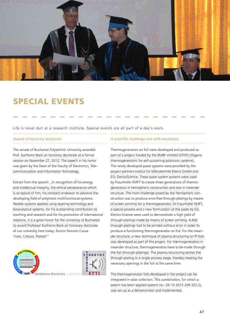
47
speciAl events
Award of honorary doctorate
The senate of Bucharest Polytechnic University awarded
Prof. Karlheinz Bock an honorary doctorate at a formal
session on November 27, 2012. The speech in his honor
was given by the Dean of the Faculty of Electronics, Tele-
communication and Information Technology.
Extract from the speech: „In recognition of his energy
and intellectual integrity, the ethical perseverance which
is so typical of him, his constant endeavor to advance the
developing field of polytronic multifunctional systems,
flexible systems applied using layering technology and
bioanalytical systems, for his outstanding contribution to
teaching and research and for his promotion of international
relations, it is a great honor for the University of Bucharest
to award Professor Karlheinz Bock an honorary doctorate
of our university here today: Doctor Honoris Causa
Vivat, Crescat, Floreat!”
L ife is never dul l at a research inst i tute. Specia l events are a l l part of a day‘s work.
A scientific challenge met with excellence
Thermogenerators on foil were developed and produced as
part of a project funded by the BMBF entitled OTEPS (Organic
thermogenerators for self-sustaining polytronic systems).
The newly developed paste systems were provided by the
project partners Institut für Mikrotechnik Mainz GmbH and
ESL ElectroScience. These paste system systems were used
by Fraunhofer EMFT to create three generations of thermo-
generators in hemispheric construction and one in meander
structure. The main challenge posed by the hemispheric con-
struction was to produce error-free through-platings by means
of screen printing for a thermogenerator. At Fraunhofer EMFT,
a special process and a new formulation of the paste by ESL
Electro-Science were used to demonstrate a high yield of
through-platings made by means of screen printing. 4,400
through-platings had to be printed without error in order to
produce a functioning thermogenerator on foil. For the mean-
der structure, a new technique of plasma structuring on PI foils
was developed as part of this project. For thermogenerators in
meander structure, thermogenerators have to be made through
the foil (through-platings). The plasma structuring etches the
through-plating in a single process stage, thereby creating the
necessary openings in the foil at the same time.
The thermogenerator foils developed in the project can be
integrated in solar collectors. This combination, for which a
patent has been applied (patent no.: DE 10 2012 209 322.2),
was set up as a demonstrator and implemented.
1

48
/ / E V E N t s A N d y O U t H d E V E l O p M E N t
1 Fraunhofer EMFT staff in
cleanroom
2 Scientist in the lab with
school students
1

49
events AnD WoRkshops
Autumn school
An event is held every year as part of the projects COSMIC,
Interflex, POLARIC and Smart-EC to allow dialogue between
the projects and present the results to a broader public.
From November 19 - 20, 2012 the latest results and fun-
damental insights from the projects were presented at
Fraunhofer EMFT in some 20 talks. The focus areas this year
were measurement and reliability of components in foil sys-
tems, materials for printed transistors on foil and materials
for electrochrome displays as part of printed electronics and
foil mounting.
Forum „Be-Flexible“
Fraunhofer EMFT has organized the international „Forum
Be-Flexible“ for over 10 years, inviting researchers, scientists,
industry partners and users to engage in a lively exchange.
In 2012, this event took place on the premises of Fraunhofer
EMFT on November 21 and 22. The event mainly focused on
the latest R&D results from the areas „Thin Semiconductor
Devices“ and „Flexible Electronic Systems“ along with their
product potential and future market prospects.
120 international participants visited the two-day event.
Fraunhofer EMFT organizes sc ient if ic events on i ts own premises every year, as wel l as present ing at
numerous external events. For example, the inst i tut ion regular ly presents i ts latest research and develop -
ment work at internat ional t rade fa i rs and congresses. Such events serve to attract new industr ia l projects
and cooperat ion partners, as wel l as a l lowing an exchange of information with potent ia l c l ients, interested
members of the publ ic and experts f rom other sc ient if ic inst i tut ions.
Here are some examples.
Fraunhofer day at Biopark Regensburg
Two Fraunhofer project groups work at the successful
Danube Innovation Center. One is Fraunhofer EMFT‘s
Sensor Materials Working Group founded in Regensburg
in 2009. The working group presented its research and
development results to the press and invited guests as part
of Fraunhofer Day on June 14, 2012. During the breaks,
experts from the Fraunhofer Board, Biopark, the University
of Regensburg and the two Fraunhofer institutes based at
Biopark made themselves available to answer questions and
engage in discussion with the approximately 60 guests.
2

50
/ / E V E N t s A N d y O U t H d E V E l O p M E N t
seMinARs AnD tRAining pRogRAMs
Esd device and design seminar
This training programs deals with the basics of characterizati-
on of integrated circuits in relation to electrostatic discharge
(ESD).
target group:
Specialists in the design and layout of I/O cells and those wor-
king in the field of measuring technology who are interested
in the ESD qualification of integrated circuits.
Microfluidics: Dosage of minute volumes
The seminar provides information on current developments in
the field of dosage modules for minute fluid quantities in the
nl range.
target group:
Specialists in analytics, medical technology, biotechnology,
mechanical engineering and process engineering.
training in cleanroom technology and cleanroom
practice, in cooperation with Vdi and tÜV sÜd
This program provides an overview of the norms and parame-
ters applicable to the design of cleanrooms. Personnel beha-
vior and test measurements in the cleanroom are illustrated
with examples.
target group:
Technologists and specialists in cleanroom technology.
1 Electronica,
Munich 2012
In order to support partners and customers, Fraunhofer EMFT offers seminars for profess ional develop -
ment, t ra in ing and information purposes which are e i ther open to the publ ic or e lse can be exc lus ive ly
ta i lored to companies‘ needs as in-house programs. Here is a smal l se lect ion of topics.
Manufacture and handling of thin silicon wafers
The seminar provides an overview of current technologies for
very thin silicon wafers and describes new concepts for car-
rier techniques based on a wide range of practical examples
from semiconductor technology.
target group:
Specialists in semiconductor technology and process
planning.
tensile strength testing of semiconductor materials
This seminar looks at current methods of analysis, the
influence of process technology on the tensile strength of
thin silicon wafers and process concepts.
target group:
Specialists in semiconductor technology, process planning
and process analysis.
self-assembly and surface programming
This seminar focuses on methods for surface programming,
analytics, practical experiments and examples of application.
target group:
Specialists in production technology and component
assembly.
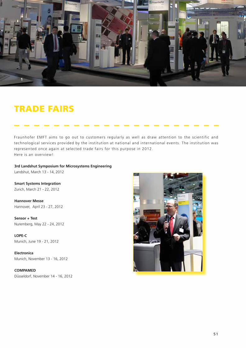
51
tRADe FAiRs
3rd landshut symposium for Microsystems Engineering
Landshut, March 13 - 14, 2012
smart systems integration
Zurich, March 21 - 22, 2012
Hannover Messe
Hannover, April 23 - 27, 2012
sensor + test
Nuremberg, May 22 - 24, 2012
lOpE-c
Munich, June 19 - 21, 2012
Electronica
Munich, November 13 - 16, 2012
cOMpAMEd
Düsseldorf, November 14 - 16, 2012
Fraunhofer EMFT aims to go out to customers regular ly as wel l as draw attent ion to the sc ient if ic and
technological serv ices provided by the inst i tut ion at nat ional and internat ional events. The inst i tut ion was
represented once again at se lected trade fa i rs for th is purpose in 2012.
Here is an overv iew!
1

52
/ / E V E N t s A N d y O U t H d E V E l O p M E N t
youth DevelopMent
work experience for school students
Fraunhofer EMFT offers 5-day work experience placements for
school students. Here the institution cooperates with various
high schools, lower secondary schools and comprehensive
schools in Munich and the surrounding area. In March 2012,
students from the Willy-Brandt-Gesamtschule and Samuel-
Heinicke-Realschule visited the Fraunhofer EMFT in Munich to
gain a first-hand impression of the institution‘s work and the
everyday working lives of scientists with a mixture of talks and
practical tasks in the lab.
talent school
In the Talent Schools of the Fraunhofer-Gesellschaft, scientists
offer a range of different workshops for young people with
an interest in technology who enjoy tackling current scientific
issues. Talks with members of the Fraunhofer management
team provide insights into the everyday work of scientific
researchers both nationally and internationally.
The title of the Fraunhofer Talent School in 2012 was „Utopia
of moving images - on wallpaper, on the cornflakes packet or
in a photo album“: 10 school students had the opportunity to
find out about the technology for assembling foil displays.
In four different laboratories, screen printing was used to print
foils as display screens, structures were applied to wafer and
foil using lithography, a control circuit was assembled and
electronic components soldered. The components were then
measured and tested for functionality.
After a very busy and intense weekend, the students were
pleased with their self-made circuits and foils and were able to
take the items home with them.
Visit by students at tU darmstadt
A 15-strong delegation from TU Darmstadt visited Fraunhofer
EMFT in June 2012 including students (electrical engineering
and information technology micromechanics and precision
engineering), lecturers and doctoral candidates. In addition
to a detailed overview of the institution, the visitors were also
given a guided tour of selected laboratory areas. Institution
scientists also presented current work on radiation detectors.
The subsequent evaluation of the event confirmed experience
to date that young people are most interested in lab presenta-
tions and the introduction to specific research projects.
1 School girls on a career
orientation placement at
Fraunhofer EMFT
Fraunhofer EMFT has been involved in promoting opportunit ies for young people in technology for a
number of years. S ince 2009 the inst i tut ion has been a partner to the „Nat ional MINT pact - more women
in MINT profess ions“ (MINT = mathematics, IT, sc ience and technology) , offer ing young people an ins ight
into the opportunit ies for t ra in ing and study in technical profess ions.

53
2
pROMOtiNg wOMEN iN MiNt pROFEssiONs
One of the purposes of career orientation weeks at Fraun-
hofer EMFT is to train school girls to be contributors for
other youth development projects. They are then able to
go on and share their knowledge with other girls.
The following youth development activities in 2012 were
especially aimed at building enthusiasm for careers in tech-
nology and science among young women.
New: Fraunhofer EMFt Vacation Academy
Two groups of 31 Allgäu students each attended the first
Fraunhofer EMFT Vacation Academy organized in colla-
boration with Kempten University. A technology rally was
offered which ran through various of the institution‘s
themes. The rally stations were:
• „Live research“
• „Cleanroom chic - dressing up for cleanliness“
• „Vacuum you can touch“
• „A micro world enlarged“
• „Are foils afraid of water?“
In this context, female Fraunhofer researchers taught practi-
cal skills in the handling and separation of wafers as well
as the structured conditioning of polymer surfaces. They
also provided an overview of some of the research areas in
which Fraunhofer EMFT is involved. When he welcomed
the participants personally, the institution‘s director Prof.
Kutter particularly emphasized the importance of female
engineers for the far-reaching work to be done in research
and development for the future of society.
workshop for female students at tU München
16 female students from various departments visited Fraun-
hofer EMFT as part of the longstanding cooperation with
the TU München mentoring program. In addition to infor-
mation on Fraunhofer and the research areas in which
Fraunhofer EMFT is involved, the students were especially
interested in measures Fraunhofer has introduced to attract
women and support them in their career planning. After the
talks and a guided tour of the laboratories, the young wo-
men took the opportunity to engage in talks directly with
female research assistants.
The following issues were of particular interest to them:
• Which areas are available for master‘s and bachelor‘s
assignments?
• Which opportunities are available to gain insights into
a research institution through placements or student
activities?
• What do scientists have to say about their experience in
their job?
• How is it possible to make contact with individual
scientists?
1

54
/ / E V E N t s A N d y O U t H d E V E l O p M E N t
shadowing day
Another interesting event is „Shadowing Day“. This event
is organized by the European Commission in collaboration
with leading companies so as to take action against the lack
of women in the field of information and communication
technologies (ICT) and show young women that ICT is not just
for „computer freaks“. Information technology is ubiquitous:
it enriches our lives, connecting people all over the world -
everywhere and all the time. It even helps save lives!
Yet there are still not enough young people opting for a career
in information and communication technologies - in particular,
there are too few women.
In 2012, as in previous years, a school girl shadowed a female
scientist for an entire working day, later reporting on her
experiences in Brussels.
young prizewinners win Fraunhofer EMFt workshop
Their outstanding entry for the „Technology Scout“ compe-
tition was recognized by the Bildungswerk der Bayerischen
Wirtschaft with a special prize.
Five school girls in the 7th grade at Pirckheimer Gymnasium,
Nuremberg, won a day at Fraunhofer EMFT: they visited
various laboratories with their teacher and carried out hands-
on activities themselves in the institution‘s cleanrooms. The
technological highlight for the students was sawing wafers.
General excitement was caused by the impact of an unintenti-
onal wafer breakage in the spin dryer.
1 Scientists in the lab with
school students
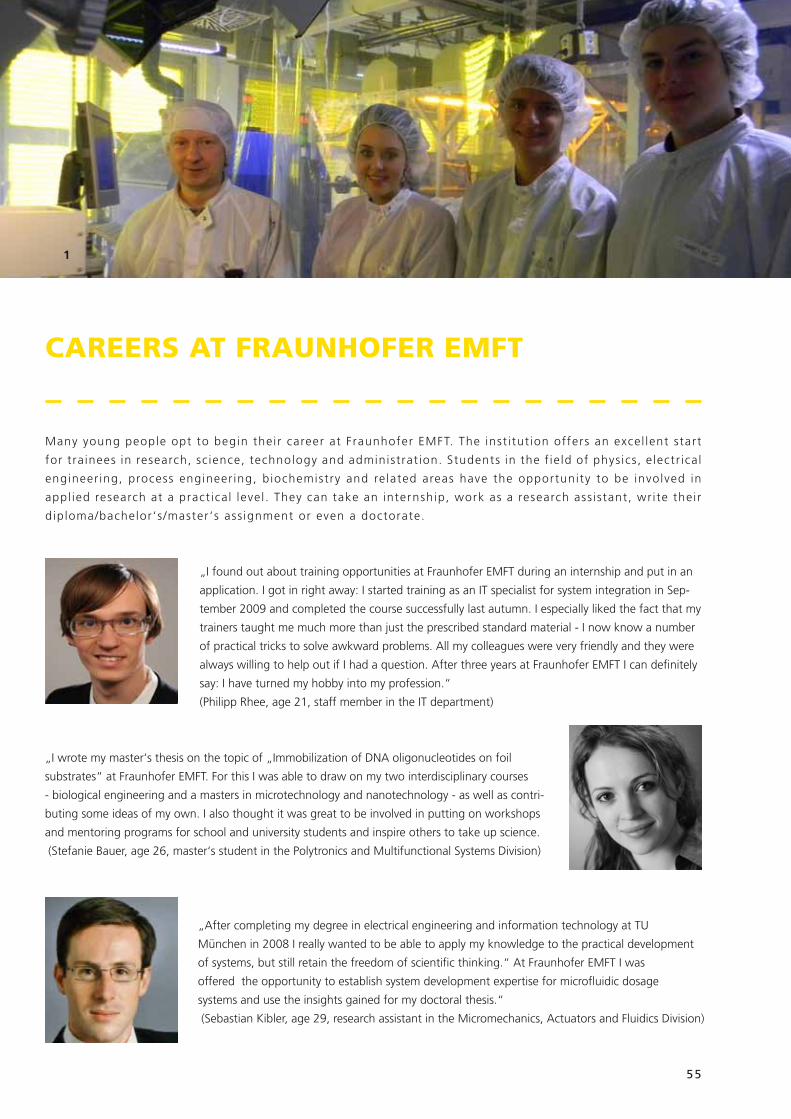
55
1
cAReeRs At FRAunhoFeR eMFt
„I found out about training opportunities at Fraunhofer EMFT during an internship and put in an
application. I got in right away: I started training as an IT specialist for system integration in Sep-
tember 2009 and completed the course successfully last autumn. I especially liked the fact that my
trainers taught me much more than just the prescribed standard material - I now know a number
of practical tricks to solve awkward problems. All my colleagues were very friendly and they were
always willing to help out if I had a question. After three years at Fraunhofer EMFT I can definitely
say: I have turned my hobby into my profession.“
(Philipp Rhee, age 21, staff member in the IT department)
Many young people opt to begin their career at Fraunhofer EMFT. The inst i tut ion offers an excel lent start
for t ra inees in research, sc ience, technology and administrat ion. Students in the f ie ld of phys ics , e lectr ica l
engineer ing, process engineer ing, b iochemistry and re lated areas have the opportunity to be involved in
appl ied research at a pract ica l level . They can take an internship, work as a research ass istant, wr i te their
diploma/bachelor‘s /master‘s ass ignment or even a doctorate.
„I wrote my master‘s thesis on the topic of „Immobilization of DNA oligonucleotides on foil
substrates“ at Fraunhofer EMFT. For this I was able to draw on my two interdisciplinary courses
- biological engineering and a masters in microtechnology and nanotechnology - as well as contri-
buting some ideas of my own. I also thought it was great to be involved in putting on workshops
and mentoring programs for school and university students and inspire others to take up science.
(Stefanie Bauer, age 26, master‘s student in the Polytronics and Multifunctional Systems Division)
„After completing my degree in electrical engineering and information technology at TU
München in 2008 I really wanted to be able to apply my knowledge to the practical development
of systems, but still retain the freedom of scientific thinking.“ At Fraunhofer EMFT I was
offered the opportunity to establish system development expertise for microfluidic dosage
systems and use the insights gained for my doctoral thesis.“
(Sebastian Kibler, age 29, research assistant in the Micromechanics, Actuators and Fluidics Division)

56
/ / p R E s s A N d M E d i A
1 Sensor system for the
detection vof CO2 in the air
1

57
Technology Review, 26.07.2012
Süddeutsche Zeitung, 17.07.2012
Aktuel le Technik, 11.07.2012

58
/ / p R E s s A N d M E d i A
Laser Photonik, 07/2012
Elektronik, 05/2012

59
Donau-Post, 15.06.2012

60
/ / p R E s s A N d M E d i A
Mitte lbayer ische Zeitung, 15.06.2012
Interpharma, 27.01.2012

61
Ärztezeitung, 19.01.2012
Onl ine-Art ikel , DeviceMed, 22.08.2012

62
/ / p R E s s A N d M E d i A
Naturhei lkunde01/2012
Mitte lstandsWiki , 07.05.2012

63
Onl ine-Art ikel , Mediz in Aspekte 05/2012
Mediz inElektronik 05/2012
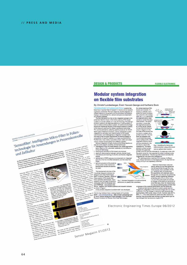
64
/ / p R E s s A N d M E d i A
Electronic Engineer ing T imes Europe 06/2012
Sensor Magazin 01/2012

65
tz-münchen, 10.04.2012

66
/ / p R E s s A N d M E d i A
PLUS, 04/2012
VµE,09/2012

67
Memminger Zeitung, 30.07.2012
Handelsblatt , 12.01.2012

68
Mikromechanisch prozes-
sierter Wafer für Höchstfre-
quenzanwendungen1/2 Multi-layer bonds of
a high-grade steel micro-
pump
1
/ / A c A d E M i c p U p l i c A t i O N s A N d t A l k s

69
AcADeMic publicAtions AnD tAlks
publications
Ohlander, A.; Hammerle, T.; Klink, G.; Zilio, C.; Damin, F.;
Chiari, M.; Russom, A.; Bock, K.
dNA melting curve analysis on semi-transparent thin
film microheater on flexible lab-on-foil substrat
Proc. of the International conference on Miniaturized
Systems for Chemistry and Life Sciences (µTAS), Okinawa,
Japan, 2012, M. 8.180
Alberti, M.; Meixner, L.; Rückerl, A.; Eder, M.; Endres, H.-E.;
Bock, K.
Sensorfilter – ein intelligentes Mikro-Filtersystem in Fo-
lientechnologie für Anwendungen in prozesskontrolle,
Zellkultur und life sciences
Procedia Engineering 47, 2012, p. 212-215
Nebrich, L.
Effektivere diagnosen durch neues sensorelement
Fraunhofer VμE Microelectronic News, September 2012, p.16
Endres, H.-E.
Intelligenter Mikrofilter überwacht seinen Beladungs-
zustand
Fraunhofer VμE Microelectronic News, June 2012, p. 9
Communicat ive exchange is very important in sc ience and research. For this reason, Fraunhofer EMFT
sc ient ists once again publ ished their in ins ights in var ious forms in 2012. The fol lowing compi lat ion is a
smal l se lect ion of the academic publ icat ions and ta lks by Fraunhofer EMFT sc ient ists .
Richter, M.
Hochdruck-Mikropumpe für anspruchsvolle
Anwendungen
Fraunhofer VμE Microelectronic News, June 2012, p. 15
Landesberger, C.; Yacoub-George, E.; Bock, K.
Modular system integration on flexible film substrates
EE Times Europe, June 2012
Nettinger, K.; Schaber, U.; Drost, A.
Anwendung des plasma-ätzens in der Rolle-zu-Rolle
prozessierung von Folien
PLUS Nr: 4, May 2012, pp. 937-1208, Bd. 14, ISSN 1436-
7505
Bock, K.
Vor-Ort-diagnostik, neuartige lab-on-a-chip-Analyse-
systeme
GIT Labor-Fachzeitschrift 4/2012
Nebrich, L.; Wiest, F.
Hochempfindliche Strahlungsdetektoren für medizini-
sche Anwendungen
Tagungsband 3., Landshuter Symposium Mikrosystemtechnik,
March 2012, pp. 245-253
2
70
/ / A c A d E M i c p U B l i c A t i O N s A N d t A l k s
Endres, H.-E.; Alberti, M.
Sensorfilter: Intelligenter Mikro-Filter in Folientechnolo-
gie für Anwendungen in prozesskontrolle und Zellkultur
Sensor Magazin 1/2012 March 2012, p. 38
Nebrich, L.
X-ray detectors to discover dangerous substances
Fraunhofer VμE Microelectronic News, March 2012, p.11
Nebrich, L.; Wiest, F., Eisele, I.
Highly sensitive Radiation detectors for Medical Appli-
cations
Proc. Smart Systems Integration, Zurich, March 2012
Garrou P.; Jian-Qiang Lu, J.; Ramm, P.
three-dimensional integration
Handbook of Wafer Bonding, Wiley VCH, ISBN 978-3-527-
32646-4, Weinheim, 2012
Klumpp, A.; Nebrich, L.; Eisele, I.
Heterogene systemintegration von Halbleitersensoren
Microsystems Technology in Germany 2012 / Mikrosystem-
technologie in Deutschland 2012, Trias Consult Johannes
GmbH, 2012, pp. 34-35
Ramm P., Lu Jian-Qiang, Taklo M.M.V. (Eds.)
Handbook of wafer Bonding
Wiley VCH, ISBN 978-3-527-32646-4, Weinheim, 2012
Klumpp, A.; Ramm, P.
Temporary Adhesive Bonding with Reconfiguration of
known good dies for three-dimensional integrated
systems
Handbook of Wafer Bonding, Wiley VCH, ISBN 978-3-527-
32646-4, Weinheim, 2012
Landesberger, C.; Klumpp, A.; Bock, K.
temporary Bonding: Electrostatic
Handbook of Wafer Bonding, Wiley VCH, ISBN 978-3-527-
32646-4, Weinheim, 2012
talks
Ramm, P.
3D Integration – Where do we need to go now?
Panel “3D Integration”, International Wafer-Level Packaging-
Conference – IWLPC 2012, San Jose, California,
November 2012
Klink, G.
Advantages of Organic and large Area Electronics for
small area devices
Forum Be-Flexible, Munich, Germany,
November 21. - 22, 2012
Bonfert, D.; Hemmetzberger, D.; Klink, G.; Bock, K.
Ageing behavior of printed flexible resistors by thermal,
mechanical and electrical stresses
COSMIC Autumn School 2012,
November 19. - 20, 2012
1 Basic unit of a high-
grade steel micropump

71
Landesberger, C.
High accuracy self-assembly of thin silicon dies
Forum Be-Flexible, Munich, Germany,
November, 21. - 22, 2012
Alberti, M.; Meixner, L.; Rückerl, A.; Eder, M.; Endres, H.-E.;
Bock, K.
Sensorfilter – ein intelligentes Mikro-Filtersystem in Fo-
lientechnologie für Anwendungen in prozesskontrolle,
Zellkultur und life sciences
4. GMM Workshop MNI, Berlin, Germany,
November 12. - 13, 2012
Ramm,P.
3d integration
Welcome Note, Proc. Sematech Workshop on Underfill
Challenges for 3D ICs, San Jose, USA, November 09, 2012
Klumpp, A.; Ramm, P.
low-temperature 3d integration processes for Reliable
Heterogeneous systems
e-BRAINS and ESiP workshop ESREF, Cagliari, USA,
October 01, 2012
Alberti, M.; Meixner, L.; Rückerl, A.; Eder, M.; Endres, H.-E.;
Bock, K.
„Sensor filter“ – Intelligent micro filter system in foil
technology
Eurosensors 2012, Krakau, Poland,
September 09. - 12, 2012
Bonfert, D.; Hemmetzberger, D.; Klink, G.; Bock, K.
Ageing behavior of printed flexible resistors by thermal,
mechanical and electrical stresses
4th Electronics System Integration Technologies Conference
ESTC 2012, Amsterdam, Netherlands,
September 17. - 20, 2012
Landesberger, C.; Scherbaum, S.; Weber, J.; Bock, K.;
Hiroshima, M.; Oberhofer, B.
plasma dicing enables high accuracy self-alignment of
thin silicon dies for 3d-device-integration
4th Electronics System Integration Technologies Conference
ESTC 2012, Amsterdam, Netherlands,
September 17. - 20, 2012
Bose, I.; Ohlander, A.; Stich, M.; Kiesl, C.; Hemmetzberger, D.;
Klink, G.; Trupp, S.; Bock, K.
polymer opto-chemical-electronic based module as a de-
tection system for volatile analytes on a foil substrate
SPIE Organic Photonics + Electronics Conference, San Diego,
USA, August 16, 2012
Trupp, S.
sensor materials and integrated packaging for smart
systems
PTS, Munich, Germany, June 13, 2012
Endres, H.-E.; Alberti, M.; Bock, K.
plastic and silicon based (bio-)chemical transducers
8th Nano-Bio Conference, Varese,
Italy, June 18. - 20, 2012
1

72
/ / A c A d E M i c p U B l i c A t i O N s A N d t A l k s
Endres, H.-E.
Elektrochemische sensoren für Umwelt und Medizin
Achema, Frankfurt, Germany, June 18. - 22, 2012
Richter, M.
TUDOS – Microdosing for Tumor Therapy
Innovationen aus Wissenschaft und Zuliefererindustrie für die
Medizintechnik, Erlangen, Germany, June 20. - 21, 2012
Trupp, S.
sensormaterialien für intelligente textilien
Innovationnetzwerk Textil e.V., Chemnitz, Germany,
June 19, 2012
Bonfert, D.; Hemmetzberger, D.; Klink, G.; Bock, K.; Svasta, P.;
Ionescu, C.
Electrical stress on intrinsically conductive polymer
layer
ISSE 2012: 35th International Spring Seminar on Electronics
Technology, Bad Aussee, Austria, May 09. - 13, 2012
Endres, H.-E.; Rose, K.; Faul, R.; Yacoub-George, E.; Bock, K.
A flexible indoor air quality system
IMCS 2012 - The 14th International Meeting on Chemical
Sensors, Nuremberg, Germany, May, 20. - 23, 2012
Richter, M.
Bioreactors with microfluidic components for tissue
engineering
Strategies in Tissues Engineering, Würzburg, Gremany,
May 23. - 25, 2012
Eisele, I.
trends in der Mikrosystemtechnik
Innovationen in Mikrosystemtechnologie 2012, Bayern Innovativ, Nuremberg, Germany, May 15, 2012
Mohr, G. J.; Hezinger, A. F. E.; Trupp, S.; Stich M. I. J.; Schmidt, J.; Wenninger, F.; Meixner, L.; Neumaier, K.; Bock, K.Fabrication of Optical sensor Materials and Modules for Food Quality control
Europtode XI, XI Conference on optical chemical sensors and biosensors, Barcelona, Spain, April 01. - 04, 2012
Nebrich, L.; Wiest, F.
Hochempfindliche Strahlungsdetektoren für medizini-sche Anwendungen
3. Landshuter Symposium für Mikrosystemtechnik, Landshut, Germany, March 13. - 14, 2012
Wieland, R.; Xuan Anh Bui, T.; Merkel K.-R.; Al Kuzee, J.Optimization of dRiE-based tsVs for 3d/MEMsMAM 2012; Workshop Materials for Advanced Metallization, Grenoble, France, March 11. - 14, 2012
Klumpp, A.
Manufacturing of 3d integrated ics
Design, Automation and Test in Europe, Dresden, Germany, March 12. - 16, 2012
Faul, R.
FuE für flexible, polytronische Systeme3. Landshuter Symposium für Mikrosystemtechnik, Landshut, Germany, March 13. - 14, 2012
1 Piezo-electrically
powered membrane
actuator

73
Weber, J.; Klumpp, A.; Ramm, P.
3d-tsV integration heterogener Mikrosysteme
3. Landshuter Symposium für Mikrosystemtechnik,
Landshut, Germany, March 13. - 14, 2012
Endres, H.-E.; Alberti, M. ; Eder, M.; Rückerl, A.; Bock, K.
Intelligenter Mikrofilter für die Mikroalgenkultur
5. Bundesalgenstammtisch, Pullach, Germany,
March 26, 2012
Nebrich, L.; Wiest, F.; Eisele, I.
Highly sensitive Radiation detectors for Medical
Applications
Smart Systems Integration, International Conference and
Exhibition on Integration Issues of Miniaturized Systems,
Zurich, Switzerland, March 21. - 22, 2012
Yacoub-Georg, E.; Bock, K.
Multifunktionale Foliensysteme für textilien
TITV-Konferenz, Zeulenroda, Germany,
February 23. - 24, 2012
1

74
/ / p A t E N t s
1 Sensor foil for parallel
measurement of O2 and
CO2
1

75
pAtents
Verpackung
Gerhard Mohr, Anna Hezinger, Sabine Trupp, Jennifer
Schmidt, Matthias Stich
DE 10 2011 075 667.1
Verfahren und Vorrichtung zum justierten laminieren
von folienbasierten schaltungsträgern zur Herstellung
von flexiblen, mehrlagigen Schaltungssubstraten
Erwin Yacoub, Christof Landesberger
DE 10 2011 004 383.7
Flexibles, mehrschichtiges schaltungssubstrat und
Verfahren zur Herstellung desselben
Robert Faul, Andreas Drost
DE 10 2011003 622.9
kleidungsstück
Dr. Gerhard Mohr, Dr. Sabine Trupp, Dr. Matthias Stich
WO 2012 / 104328
Verfahren zur Herstellung eines chip-package
Christof Landesberger, Robert Faul
DE 10 2010 042 567.2
Organischer transistor und Verfahren zur Herstellung
desselben
Markus Burghart, Gerhard Klink
DE 10 2010 061 978.7
The fol lowing Fraunhofer EMFT patents were disc losed in 2012:
Microfluidic device, microfluidic dosing system
Martin Richter, Sebastian Kibler
WO 2012 031630
Method for manufacturing a three-dimensional electronic
system
Peter Ramm, Armin Klumpp
US 2010/0289146

76
1 Fraunhofer scientist
holding a MEMS wafer
2 MEMS microphone
wafer
/ / M E M B E R s H i p s A N d A c t i V i t i E s
1

77
MeMbeRships AnD Activities
prof. dr. rer. nat. christoph kutter
• IEEE Components, Packaging & Manufacturing Techno-
logy Society and Electron Devices Society: Member
• Deutsche Physikalische Gesellschaft: Member
• Association for Electrical, Electronic & Information
Technologies (VDE): Member
• VDE GMM (Gesellschaft für Mikroelektronik, Mikro-
mechanik und Feinwerktechnik): Deputy Chairman
• Innovationspreis der deutschen Wirtschaft: Member of
the awards advisory board
• VDI VDE IT GmbH: Member of the Supervisory Board
prof. dr.-ing. dr. h. c. karlheinz Bock
• AMA, AMA Wissenschaftsrat und AMA Sensor-Innovati-
onspreis: Member
• Arbeitsgemeinschaft Organic Electronics Association OEA,
VDMA: Member
• Compound Semiconductor Manufacturing Technology,
CS MANTECH, USA: Member of the Technical Program
Committee
• EITI – European Interconnect Techology Initiative: Member
• FlexTech Alliance, USA: International Advisory Board
• Forum MedTech Pharma, Bayern Innovativ: Member
• Institute of Electrical and Electronics Engineers IEEE: Member
• IEEE Components, Packaging & Manufacturing Techno-
logy Society and Electron Devices Society: Member
• International Electronic Components and Technologies
Conference, ECTC, USA: Sub-committee chair„Emerging
technologies“
• International Electron Devices Meeting IEDM, USA:
Member of the Executive Committee and European
Arrangement Chair
• International Conference on Flexible and Printed Electro-
nics (ICFPE), Japan: European Committee
• Micro- and Nanotechnology Journal der Bentham Science Pu-
blisher Ltd.: Member of the Board of Editors and Consultant
• MRS - Materials Research Society: Member
• Plastic Electronics Conference: Conference cochair for the
Integrated Smart Systems Conference part
• IEEE Electron Devices Letters EDL: Consultant
• Applied Physics Letters APL: Consultant
• German Israeli Foundation for Scientific Research and typo
Development (G.I.F): Consultant
• Electronics Systems Integration Technology Conference
ESTC, Technical Program Committee: Member
• Journal of Micromachines: Consultant
• VDE und Kerngruppe des Arbeitskreises für Mikroelektro-
nik und Feinwerktechnik: Member
• Smart Systems Integration Conference, SSI: Technical
Program Committee and Founding Member
• Design and Technology in Electronic Packaging
(SIITME): Member of the Steering Committee
• Interconnection techniques in Electronics (TIE contest):
Member of the Steering Committee
Fraunhofer EMFT staff promote the transfer of knowledge through membership of a wide range of diffe-
rent networks and cooperat ions. This enables them to tackle interdisc ip l inary tasks beyond the bounds of
the Fraunhofer inst i tut ion i tse lf .
2

78
// Mitgliedschaften und Aktivitäten
prof. dr. rer. nat. ignaz Eisele
• Robert Bosch Zentrum Reutlingen: Member of the
Advisory Board
• IHP, Frankfurt/Oder: Member of the Scientific Advisory
Board
prof. dr. techn. linus Maurer
• IEEE, Institute of Electrical and Electronics Engineers:
Member
• ITG Informationstechnische Gesellschaft im VDE: Member
• VDE Verband der Elektrotechnik Elektronik Informations-
technik e.V.: Member
• IEEE MTT-27 (wireless-enabled automotive and vehicular
applications): Member
dr. rer. nat. peter Ramm
• International Microelectronics and Packaging Society
iMAPS: Fellow of Society and Life Member
• Electronic Components and Technologies Conference
(ECTC): Sub-Committee Advanced Packaging
• International Microelectronics and Packaging Society
iMAPS: Award Committee
• iMAPS Device Packaging Conference (iMAPS DPC):
Technical Co-Chair 3D Packaging
• Sematech ITRS Interconnect Working Group:
Key Contributor
• SEMI North America: Committee Standards 3DS-IC,
Technical Committee
• Electrochemical Society (ECS): Symposium Organizer
• Institute of Electrical and Electronics Engineers IEEE:
Organizing Committee and Founding Member
3DIC Conference
• Future Fab International Magazine: Editorial Board
Member
• Advanced Metallization Conference (AMC): Executive
Committee
• Surface Mount Technology Association (SMTA): Technical
Committee Member IWLPC and 3D Integration Chair
dr.-ing. Martin Richter
• VDE/VDI-Gesellschaft Mikroelektronik, Mikro- und Fein-
• werktechnik (GMM), Fachbereich 2; Mikro- und Nano-
technik, Fachausschuss 2.4 „Mikroaktorik“: Member
• Association Multi Material Micromanufacturing (4M):
Head of division microfluidics
• MST Kongress: : Member of program committee
dr.-ing. detlef Bonfert
• IEEE, Institute of Electrical and Electronics Engineers:
Senior Member
• IEEE, Society: CPMT, EDS, CS, MTT: Member
• International Microelectronics and Packaging Society-
iMAPS: Member
• International Symposium for Design and Technology in
Electronic Packaging SIITME, Technical Program Commit-
tee Chair, Steering Committee and Scientific Committee
Member
• International Spring Seminar in Electronics ISSE: Steering
Committee Member
/ / / / M E M B E R s H i p s A N d A c t i V i t i E s
1 Fraunhofer scientist
with MEMS wafer

79
• Design of Electronic Modules and Assemblies, TIE:
Technical Committee Member
dieter Bollmann
• Fraunhofer-Gesellschaft: Elected Representative on the
Scientific Technical Council
dr.-ing. Hanns-Erik Endres
• Cluster-Offensive Bayern, Cluster Sensorik: Member and
Technical Advisor
• Fraunhofer-Netzwerk Elektrochemie: Member
Robert Faul
• Hochschule Landshut, Cluster Mikrosystemtechnik:
Technical Advisor
• Cluster-Offensive Bayern, Cluster Mechatronik und
Automation: Technical Advisor
dr.-ing. Horst A. gieser
• ESD-FORUM e.V.: Board Chairman and Founding Member
• Industry Council on ESD-Target Levels: Member
• EOS/ESD Association, USA: Member
• EOS/ESD Symposium, USA: Technical Program Committee
• International Electrostatic Workshop IEW: Management
Committee
• European Symposium on Reliability of Electron Devices,
Failure Physics and Analysis ESREF: Technical Program
Committee
• EOS/ESD Association, USA: Member
• EOS/ESD Symposium, USA: Technical Program Committee
• International Electrostatic Workshop (IEW): Technical
Program Committee
dr. rer. nat. Armin klumpp
• International Electron Devices Meeting IEDM, USA:
Technical Committee
christof landesberger
• Cluster-Offensive Bayern, Cluster Leistungselektronik:
Technical Advisor
sabine scherbaum
• ZAK-Zentrum für angewandte Kompetenz und Mentoring
der Frauenakademie München: Mentor
• mst|femNet meets Nano and Optics in: Nationalen Pakt
für Frauen in MINT-Berufen: Fraunhofer EMFT Advisor
dr.-ing. Heinrich wolf
• EOS/ESD Association, USA: Member
• EOS/ESD Symposium, USA: Technical Program
Committee
• International Electrostatic Workshop (IEW): Technical
Program Committee
Axel wille
• Deutsche Physikalische Gesellschaft: Member
• VDI Verein Deutscher Ingenieure: Member
1


![Prof. Dr. Paul Seidel VL Festkörper MaWi WS 2013/141 15. Magnetische Eigenschaften der Festkörper Magnetit [ mineralienatlas.de ]](https://img.dokumen.tips/doc/110x75/55204d8449795902118d8cb1/prof-dr-paul-seidel-vl-festkoerper-mawi-ws-2013141-15-magnetische-eigenschaften-der-festkoerper-magnetit-mineralienatlasde-.jpg)