Embed Size (px)
Citation preview

FPGAs in Flash Controller
Applications and More
David McIntyre
Altera Corp.
Flash Memory Summit 2014
Session 102-C
Tues August 5, 9:45am
1
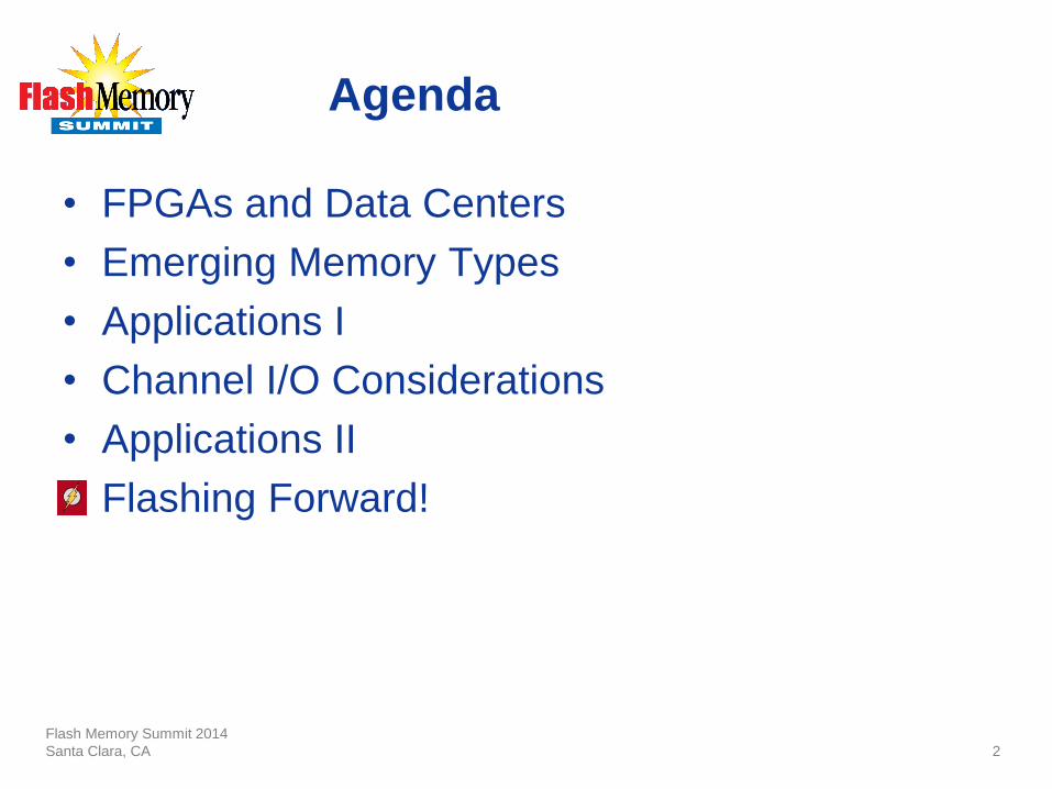
Agenda
Flash Memory Summit 2014
Santa Clara, CA
• FPGAs and Data Centers
• Emerging Memory Types
• Applications I
• Channel I/O Considerations
• Applications II
• Flashing Forward!
2
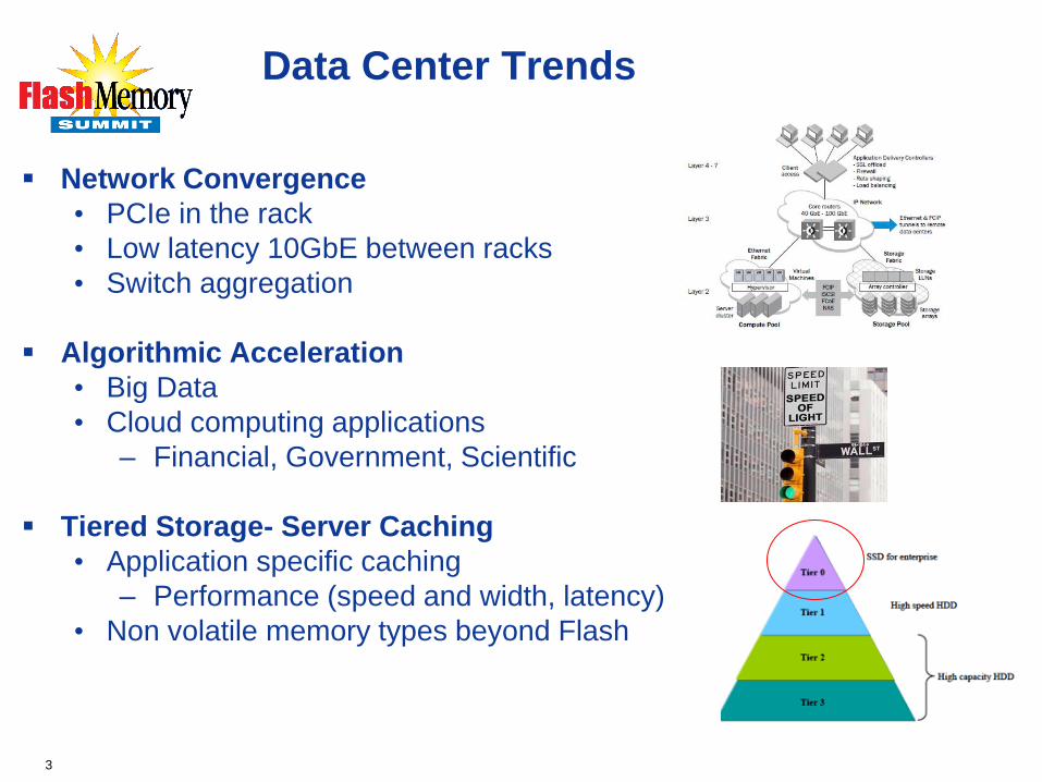
Data Center Trends
Network Convergence
• PCIe in the rack
• Low latency 10GbE between racks
• Switch aggregation
Algorithmic Acceleration
• Big Data
• Cloud computing applications
– Financial, Government, Scientific
Tiered Storage- Server Caching
• Application specific caching
– Performance (speed and width, latency)
• Non volatile memory types beyond Flash
3

TEST & MEASUREMENT
FPGA Utilization across Data Centers
Point and SOC Solutions
• Application Acceleration
• Embedded Processing
• I/O Protocol Support
• Memory Control
• Compression
• Security
• Port Aggregation & Provisioning
4
R&D,
Integration
Protocol
Conformance
Test
Application
Performance
Trials
Deployment Monitoring
&
Upgrades
Application Acceleration
Flash Memory Summit 2014
Santa Clara, CA
5

Technology scaling favors programmability and parallelism
6
CPUs DSPs Multi-Cores Array GPGPUs FPGAs
Fine-Grained Massively Parallel Arrays
Single Cores Coarse-Grained Massively Parallel Processor Arrays
Multi-Cores Coarse-Grained CPUs and DSPs
Processing Options

Altera FPGA Technology –
Hardware Programming
Massive Parallelism • Millions of logic elements
• Thousands of 20Kb memory blocks
• Thousands of DSP blocks
• Dozens of High-speed transceivers
Hardware-centric • VHDL/Verilog
• Synthesis
• Place&Route
7
I/O
I/O
I/O
I/O
Programmable
Routing Switch
Logic
Element
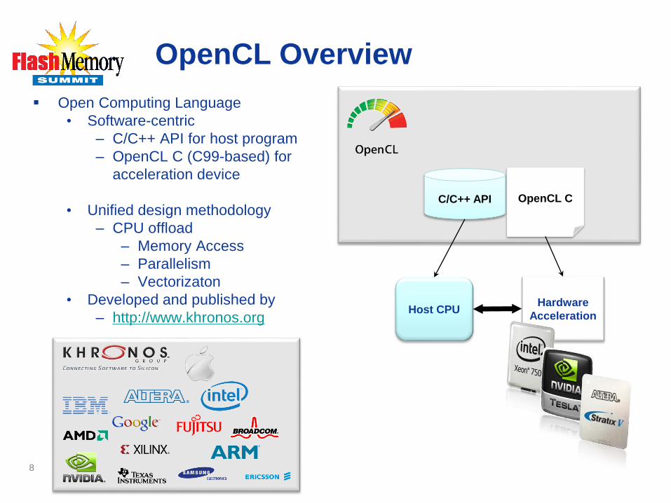
OpenCL Overview
Open Computing Language
• Software-centric
– C/C++ API for host program
– OpenCL C (C99-based) for
acceleration device
• Unified design methodology
– CPU offload
– Memory Access
– Parallelism
– Vectorizaton
• Developed and published by
– http://www.khronos.org
8
Host CPU Hardware
Acceleration
C/C++ API OpenCL C

x86
OpenCL Process
9
PCIe
Altera OpenCL
Compiler Standard
C Compiler
AOCX EXE
OpenCL
Host Program + Device Kernels
Verilog
Quartus II
main() { read_data( … ); manipulate( … ); clEnqueueWriteBuffer( … ); clEnqueueNDRange(…,sum,…); clEnqueueReadBuffer( … ); display_result( … ); }
__kernel void sum(__global float *a, __global float *b, __global float *y) { int gid = get_global_id(0); y[gid] = a[gid] + b[gid]; }

Multi-Asset Barrier Option Pricing
Monte-Carlo simulation
• Heston Model
• ND Range – Assets x Paths (64x1000000)
Advantage FPGA
• Complex Control Flow
Results
10
Platform Power
(W)
Performance
(Msims/s)
Msims/W
W3690 Xeon Processor 130 32 0.25
nVidia Tesla C2075 225 63 0.28
PCIe385 D5 Accelerator 23 170 7.40
tttt
S
ttttt
dWdtd
dWSdtSdS

GZIP Comparison
11
Same compression ratio
12X better performance/Watt

Storage Trends
Flash Memory Summit 2014
Santa Clara, CA
12

Volatile vs NVM Market Share
13
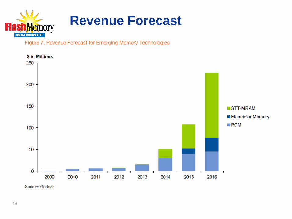
Revenue Forecast
14

Flash Cache Challenges & Evolution
Ongoing Challenges • Error correction costs increasing
• Limited endurance (lifetime writes)
• Slow write speed
• SATA/SAS SSD interface is slow
Storage over PCIe • Faster BW projections
• SATA Express
• NVM Express
• SCSI Express
Emerging flash technologies • MRAM (Magneto Resistive)
• PCM (Phase Change)
• RRAM (Resistive)
• NRAM (Carbon Nanotube)
15

Tiered Storage, Then
16
Seminole Indian Storage
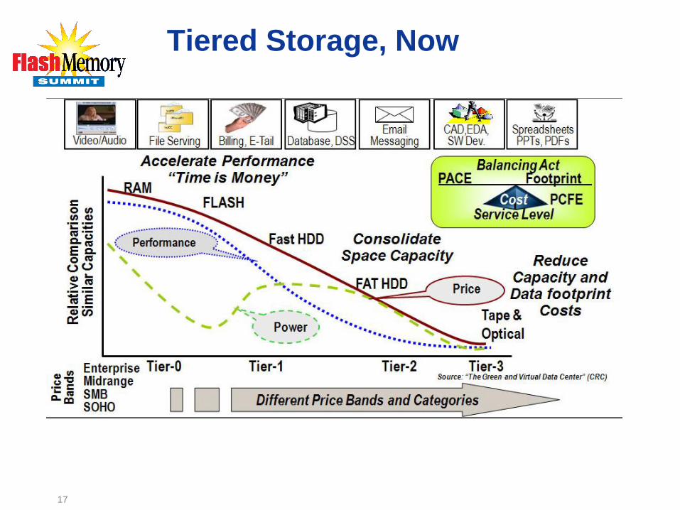
Tiered Storage, Now
17

Flexibility Required to Support
Emerging Memory Technologies
Flash Memory Summit 2014
Santa Clara, CA
18

Hybrid Memory Cube (HMC)
19
HMC technology basics Ultra high performance, multi-bank DRAM memory
DRAM die stacked using state-of-the-art 3D process
Built-in memory controller with logic base die
Unparalleled gains with HMC Maximum DRAM bandwidth of up to 160 GB/s
Four links running at 15 Gbps offering nearly 1 T bps raw interface bandwidth
Up to 4GB density (storage) capacity, low PHY power (pj/bit)
Best in class RAS feature set
Parameters Specification
Link 4
Speed 10,12.5,15 Gbps
Density 2GB, 4GB
Vaults 16
Banks 128, 256
DRAM B/W 160 GB/s (1.2 Tbps)
Vault B/W 10 GB/s (80 Gb/s)

Memory Categories
20

Memory Comparison
21
Figure 2 shows a comparison of these emerging memory technologies. We compare the properties
of most memory technologies in reading speed (x-axis), endurance (y-axis), cell size (size of the ball)
and switching energy (color of the ball).

Memory Comparisons- Performance
22

Migration Timeline- Cost
23

5MB in Flight!
24

Convergence.
Let’s Win and have Fun!
25

26
Data Center Applications- Servers
Co-ASIC
Application
Bridge Plus
Acceleration
I/O Virtualization
(10GbE and PCIe)
Management
(BMC, KVM)
Mainframe
Blade Server
Accelerator Card
Flash SSD
Flash Controller
Usage Examples
Interface bridging with IP
function, e.g. compression and
encryption, Dedupe
Algorithm acceleration for
vertical markets
ASIC alternative; low cost
with flexibility
IP Flexibility supported with
low power
Features enhancement
PCIe to ONFI bridging,
Flash Control

27
Data Center Applications- Storage
Application Usage Examples
Flash Cache/SSD ONFI bridging and RAID adaptor NV
DIMM backup, RAID for Flash
RAID Bridging PCIe Gen 3 x8 best of class signal integrity
Bridge Plus Interface bridging with IP function
ASIC Replacement Lower cost development with flexibility
Tape
Memory BackUp/Restore

Hybrid RAID System
- Persistent DRAM and Flash Caches
FC, iSCSI,
FCoE
CPU
PCI-e SATA
SAS
Network
Side
Persistent
DRAM
FC HBA
PCI-e or CPU System Bus
FC HBA
CPU Interface
Cache/Memory Controller
Network
I/F
Disk
I/F RAID²
Logic PCI-e
PCI-e
Disk
Side
FPGA Controller
ASSPs
RAID/Cache Controller
Flash
Cache
Dual
Controller

Hybrid RAID System
- PCIe Switch Centric
FC, iSCSI,
FCoE
CPU
PCI-e SATA
SAS
Network
Side
Persistent
DRAM
FC HBA
PCI-e or CPU System Bus
FC HBA
PCI-e
PCI-e
Disk
Side
FPGA Controller
ASSPs
PCIe Switch
Dual
Controller
Dedupe/
Encrypt Flash Cache
PCI-e PCI-e
Flash Controller Design
Considerations
Flash Memory Summit 2014
Santa Clara, CA
30

Flash Controller Requirements
Uncertainty Favors PLDs for Flash Control Solutions
Flash Challenges Continue
• Data loss, slow writes, wear leveling, write amplification, RAID
Many Performance Options
• Write back cache, queuing, interleaving, striping, over provisioning
Many Flash Cache Opportunities
• Server, blade and appliance

Flash Controller Design Challenges
Flash Memory Summit 2012
Santa Clara, CA
32
Emerging memory types
- ONFI 4.0, Toggle Mode 2.x
- PCM, MRAM
- DDR4 Controller Performance Options
- Write back cache, queuing, interleaving, striping
ECC levels
- BCH, LDPC, Hybrid
FTL location- Host or companion
Data transfer interface support
- PCI Express, SAS/SATA, FC, IB
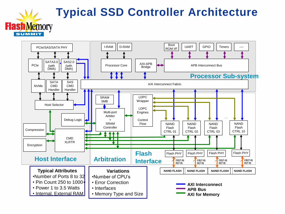
Typical SSD Controller Architecture
AXI Interconnect APB Bus AXI for Memory
SATA3.0
(with DMA)
Compression
Processor Core
Multi-port
Arbiter
+
SRAM
Controller NAND
Flash
CTRL 01
Boot
ROM I/F I-RAM
NAND
Flash
CTRL 02
NAND
Flash
CTRL 03
NAND
Flash
CTRL 10
…
AXI Interconnect Fabric
NAND FLASH
CE(7:0) D(7:0)
CE(7:0) D(7:0)
CE(7:0) D(7:0)
CE(7:0) D(7:0)
D-RAM
AXI-APB Bridge
APB Interconnect Bus
UART GPIO Timers ---- PCIe/SAS/SATA PHY
Host Selector
Encryption
SATA
CMD
Handler
SAS
CMD
Handler
CMD
XLRTR
LDPC
Wrapper
LDPC
Engines
Control
Flow
SRAM
5MB
Debug Logic
SAS2.0
(with DMA)
Processor Sub-system
Host Interface Flash
Interface Arbitration
NAND FLASH NAND FLASH NAND FLASH
PCIe
NVMe
Flash PHY Flash PHY Flash PHY Flash PHY
Typical Attributes
•Number of Ports 8 to 32
• Pin Count 250 to 1000+
• Power 1 to 3.5 Watts
• Internal, External RAM
Variations
•Number of CPU’s
• Error Correction
• Interfaces
• Memory Type and Size

Mobiveil NVMe SSDC Solution
8/5/2014 34
On Chip AXI Interconnect
On Chip APB Interconnect
Inter block AXI Interconnect
Avalon MM
Bridge*
NVMe Controller
(UNEX)
ARM Hard
IP
Altera DDR3 Hard IP
PCIe
NVMeFW
Interconnect
Altera PCIe Hard
IP
• DDR3
• NAND
• MRAM

Error Correction Overview
Driving Factors for New
ECC
Comparing ECC Solutions
Features BCH LDPC
Gate
Count
High Mid
Latency Low Medium
Tuneablity low high
Soft Data no high
Data
Overhead
high low
35
198X 199X Present
Combined ECC
Increasing Bit errors in NAND Flash
Soft error occurrences
Decrease in write cycles
RS, BCH overhead for data and spare area
Increase use of Metadata in file systems
Correction Overhead
Gate count
Requirement for no data loss

The Parade of Codes
Flash Memory Summit 2014
Santa Clara, CA
36
ECC- Block Hamming - DRAM variant
- Applicable to the flash page block sizes
- Smaller blocks used as error rates increased
Reed Solomon - CD-ROM basis, stronger than Hamming - Split correction blocks split into 9 bit symbols - Good for clumped errors
BCH
- Better supports MLC >8bits correction block
- BCH ECC increasing with correction block sizes

LDPC and Programmable Logic
Addresses higher BER across process node curve
Good for TLC
FPGA parallelism of Parity Matrix allows for faster
processing of algorithm
Flash Memory Summit 2014
Santa Clara, CA
37

Flash Controller Support
IP IO Speed Logic Density Comments
ONFI 3.0 40 pins/ch 400 MTps 5KLE/ch NAND flash control, wear
leveling, garbage collection
Toggle
Mode 2.0
40 pins/ch 400 MTps 5KLE Same
DDR3 72 bit 1066 MHz 10KLE Flash control modes available
for NVDIMM
PCM
MRAM
5KLE
5KLE
PCM- Pending production $
MRAM- Persistent memory
controller (Altera based)
BCH <10KLE Reference design
PCIe G3x8 64Gbps HIP Flash Cache

Flash Storage Arrays
PCIe Gen 3x8
Flash
Memory
Flash
Control RAID Control
LVDS
Power
Mgt
Function Solution
Rqts
Target
Product
IP Rqts
Flash Control -ONFI 2.X/3.0
-Toggle Mode 2.0
- Multi flash load/ch
- 40 GPIO/ch
Arria V
(28nm)
- Flash Controller
(bad block mgt and
wear leveling)
- Metadata & caching
- ECC BCH core
RAID Control PCIe Gen 3
Arria 10
(20nm)
- Flash-specific RAID
- Switching and
aggregation
Power Mgt Enpirion
Target Application: Enterprise Tier-1 Storage: Databases and Virtualization

Flash PCIe Cards
Flash
Memory
Flash
Controller
DRAM
PCIe: Gen 3x8
Function Solution
Rqts
Target
Product
IP Rqts
Flash
Control
-ONFI 2.X/3.0
-Toggle Mode 2.0
- Multi flash load/ch
-40 GPIO/ch
-PCIe Gen 3 x8
-Low power & cooling
Arria V
Arria 10
- Flash Controller
(bad block mgt and wear
leveling)
-Flash RAID
-Cache controller
- BCH core
-PCIe config < 100msec
-Host interface/APIs
Target Application: Embedded PCIe storage for flash cache and scale-out computing
FPGA controller provides flexiblity to integrate
multiple complex functions and adapt to
changing interfaces & APIs.

Flash Cache Controller Examples
Multi Channel Controller
• Single to multi Flash
channel capability
• Basic NAND
development platform
• Provides High Speed
ONFI & Toggle NAND
PHY
• ECC of 8 and 15 bits of
error correction
Single Channel Controller
DMA
CPU
AV
AL
ON
SW
ITC
H F
AB
RIC
Avalon Master
Interface
Avalon Slave
Interface
Two
Buffers
Control
Registers
FSM
ECC
NAND Flash

PCIe to RAID controller
Flash
(NVDIMM)
Flash Control
RAID
PCIe Gen 3 x8
Function Solution
Rqts
Target
Product
IP Rqts IP Partner
RAID
Control
-ONFI 2.X/3.0
-Toggle Mode 2.0
- Multi flash load/ch
-40 GPIO/ch
-PCIe Gen 3
-6Gb SAS/SATA
Arria 10
Flash Controller
RAID
PCIe config < 100msec
6Gb SAS/SATA
SLS
CAST
Altera Reference Design
(3Q12)
CEVA/Inteliprop
Target Application
Embedded storage for flash cache and high performance computing
SSD
Interface (SAS/SATA)
PCIe
Gen 2x4 CPU

Memory Lookup and Cache
Flash
High Speed
Serial Bridge PCIe Gen 3 x8
Functio
n
Solution
Rqts
Target
Product
IP Rqts IP Partner
Memory
Control
-ONFI 2.X/3.0
-Toggle Mode 2.0
- Multi flash load/ch
-40 GPIO/ch
-PCIe Gen 2 x8/Gen3 x8
-Interlaken
Arria V
Arria 10
Flash Controller
PCIe config < 100msec
6Gb SAS/SATA
“Look-aside variant”
SLS
CAST
Target Application
Embedded Memory search and cache for high performance computing
Interlaken
Look Aside
DRAM
Memory
Search
Engine

Development Platforms
Everspin
64MB DIMM
Stratrix/Arria FPGA
Gidel ProceV Board
44
Cyclone Development Board
Micron Daughter Card
Introspect
I/O Tester

System IO Considerations
Flash Memory Summit 2014
Santa Clara, CA
45

System IO
Flash Memory Summit 2012
Santa Clara, CA
46
System Application Requirements Performance- bandwidth
IO network
Memory
Latency
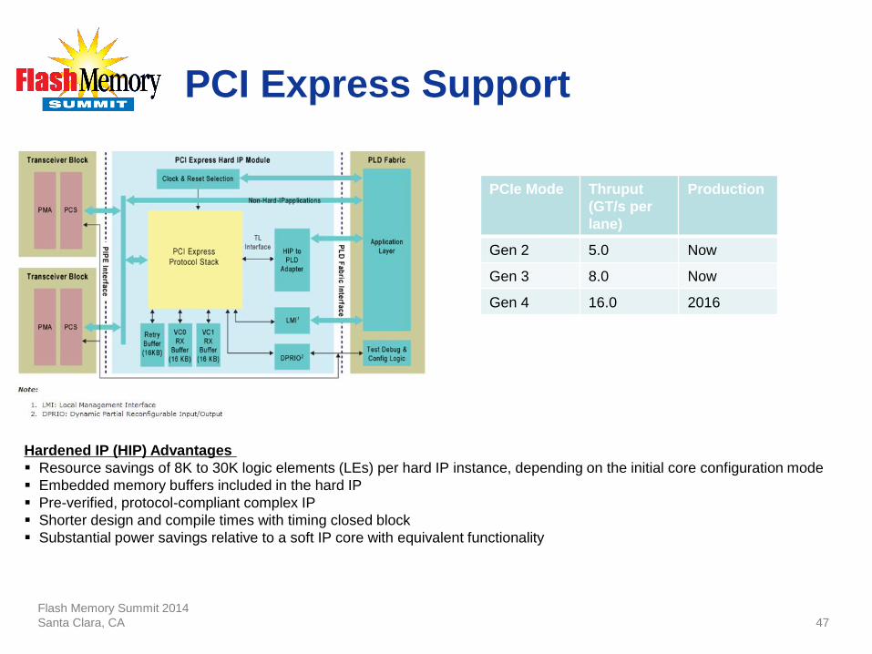
PCI Express Support
Flash Memory Summit 2014
Santa Clara, CA
47
Hardened IP (HIP) Advantages
Resource savings of 8K to 30K logic elements (LEs) per hard IP instance, depending on the initial core configuration mode
Embedded memory buffers included in the hard IP
Pre-verified, protocol-compliant complex IP
Shorter design and compile times with timing closed block
Substantial power savings relative to a soft IP core with equivalent functionality
PCIe Roadmap
PCIe Mode Thruput
(GT/s per
lane)
Production
Gen 2 5.0 Now
Gen 3 8.0 Now
Gen 4 16.0 2016

PCI Express NVMe
Flash Memory Summit 2014
Santa Clara, CA
48
Scalable host controller interface for PCIe-based
solid state drives
Optimized command issue and completion path
Benefits
Software driver standardization
Direct access to flash
Higher IOPS and MB/s
Lower latency
Reduced Power Consumption
Software

Intel QPI
Up to (2) full width QPI 1.1 • 6.4, 8.0 Gbps
Designed for QPI Electricals • Common Mode Voltage
• Lane detection on die
Chip to chip interconnectivity
Fast HP 28nm. process
Hard PHY + Upper Layers Option • Decrease latency, power, & fpga logic
• Use “Embedded Hardcopy Blocks”
• Improve throughput by 75+%
– 6-8GB/s data payload each way

50
Industry Interface Convergence

SAS/SATA
Flash Memory Summit 2014
Santa Clara, CA
51
Flash Controllers manage SAS/SATA SSD interfaces
12Gbps SAS support required for enterprise drives
FPGA transceivers need to support electrical performance
and OOB signaling

6G SAS Demo
PC running SSD Emulation Windows Driver or CEVA SASTool test software
(as if embedded processor)
PCIe Interface
SAS Cable Connection to
SAS peer (via connector
mezzanine board) AHB-to-PCIe Bridge
PCIe macro
SAS FPGA
Data
PathDMA
ST
P
TT
SM
P
MT
SS
P
ST
Po
rt P
L_
PM
ST
P
Lin
k
SM
P
Lin
k
SS
P
Lin
k
Lin
k S
L
PH
Y C
ontr
ol
Control Interface
Em
bed
ded
Ser
des
SAS peer is Lecroy SAS
Sierra M6-2 or various SAS HDD

FPGA Flash Applications- Part Two
Flash Memory Summit 2014
Santa Clara, CA
53
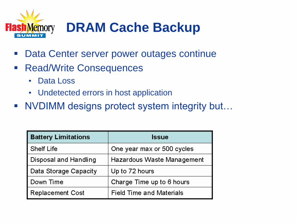
DRAM Cache Backup
Data Center server power outages continue
Read/Write Consequences
• Data Loss
• Undetected errors in host application
NVDIMM designs protect system integrity but…

The Perfect Storm
Technology Enablers
• Super Capacitors are production worthy
• Flash memory costs continue to decline
• FPGA technology meeting power/performance/cost
Lower Cost per Process Node Step FPGA Low Power Attributes

Memory Backup Target Application
Nonvolatile DIMM for data recovery backup and restore
FET
Flash

57
NVDIMM Controller Architecture
Processor DDR
FPGA
(Cyclone)
FET
bank 400MHz /
800MB tested
DIMM
Can be
• Buffered
• Un-buffered
• Registered
On power failure these FETs
switch out the processor
signals
Flash
1 or 2 SD
Cards or BGA
DDR ctrl with tri-state Power
regulation
To super-cap
bank
I2C
Control
signals
Individual CKE lines
5 or 9
Power failure
switch

MRAM
58

59
FPGA Benefits Summary
High System Performance
Design Flexibility
Low Power
Embedded Processing
Signal Integrity
Memory Bandwidth

Flashing Foward
FPGAs are a great technology option for Data
Centers
• Networking: Port aggregation
• Compute: Application Acceleration
• Storage: Controllers for non volatile memories
All development phases supported
• Prototyping
• Production
• Test Validation
• Upgrades
60

Innovation Leader Across the Board
61
CPLDs
Lowest Cost,
Lowest Power
PowerSoCs
High-efficiency
Power Management
FPGAs
Cost/Power Balance
SoC & Transceivers
Design Software
Development Kits
Embedded Soft and Hard Processors
FPGAs
Mid-range FPGAs
SoC & Transceivers
R E S O U R C E S
FPGAs
Optimized for
High Bandwidth
Intellectual Property (IP)
Industrial
Computing
Enterprise
Exhibit
Booth
320