Embed Size (px)
Citation preview

© 2016 WILEY-VCH Verlag GmbH & Co. KGaA, Weinheim
p s scurrent topics in solid state physics
c
stat
us
soli
di
www.pss-c.comph
ysic
aPhys. Status Solidi C 13, No. 10–12, 870–881 (2016) / DOI 10.1002/pssc.201600083
Field- and irradiation-induced phenomena in memristive nanomaterials A. N. Mikhaylov*,1, E. G. Gryaznov1, A. I. Belov1, D. S. Korolev1, A. N. Sharapov1, D. V. Guseinov1, D. I. Tetelbaum1, S. V. Tikhov1, N. V. Malekhonova1, A. I. Bobrov1, D. A. Pavlov1, S. A. Gerasimova1, V. B. Kazantsev1, N. V. Agudov1, A. A. Dubkov1, C. M. M. Rosário2, N. A. Sobolev2, and B. Spagnolo3
1 Lobachevsky University, 23/3 Gagarin prospect, 603950 Nizhny Novgorod, Russia 2 Departamento de Física and I3N, Universidade de Aveiro, 3810-193 Aveiro, Portugal 3 Dipartimento di Fisica e Chimica, Università di Palermo, Group of Interdisciplinary Theoretical Physics and CNISM,
Unità di Palermo,Viale delle Scienze, Ed. 18, 90128 Palermo, Italy
Received 31 May 2016, revised 29 August 2016, accepted 5 October 2016 Published online 20 October 2016
Keywords memristor, resistive switching, metal-oxide-metal nanostructure, kinetic Monte-Carlo simulation, radiation tolerance, synaptic behaviour, nonlinear dynamics, stochastic resonance * Corresponding author: e-mail [email protected], Phone: +7 831 4623188, Fax: +7 831 4623136
The breakthrough in electronics and information technol-ogy is anticipated by the development of emerging mem-ory and logic devices, artificial neural networks and brain-inspired systems on the basis of memristive nano-materials represented, in a particular case, by a simple ‘metal–insulator–metal’ (MIM) thin-film structure. The present article is focused on the comparative analysis of MIM devices based on oxides with dominating ionic (ZrOx, HfOx) and covalent (SiOx, GeOx) bonding of vari-ous composition and geometry deposited by magnetron sputtering. The studied memristive devices demonstrate reproducible change in their resistance (resistive switch-ing – RS) originated from the formation and rupture of conductive pathways (filaments) in oxide films due to the electric-field-driven migration of oxygen vacancies and / or mobile oxygen ions. It is shown that, for both ionic and covalent oxides under study, the RS behaviour de-
pends only weakly on the oxide film composition and thickness, device geometry (down to a device size of about 20×20 μm2). The devices under study are found to be tolerant to ion irradiation that reproduces the effect of extreme fluences of high-energy protons and fast neu-trons. This common behaviour of RS is explained by the localized nature of the redox processes in a nanoscale switching oxide volume. Adaptive (synaptic) change of resistive states of memristive devices is demonstrated under the action of single or repeated electrical pulses, as well as in a simple model of coupled (synchronized) neu-ron-like generators. It is concluded that the noise-induced phenomena cannot be neglected in the consideration of a memristive device as a nonlinear system. The dynamic response of a memristive device to periodic signals of complex waveform can be predicted and tailored from the viewpoint of stochastic resonance concept.
© 2016 WILEY-VCH Verlag GmbH & Co. KGaA, Weinheim
1 Introduction The effect of resistive switching (RS) was discovered in the last century [1] but only now it is be-ing actively employed in the development of so called memristive devices as a basis of new generation electronic systems. The ideal memristor was mathematically defined by Chua [2] as a two-terminal device whose resistance de-pends on internal state variables irrespective of their physi-cal interpretation. In the case of a solid-state RS device, the resistance change can be realized in a very simple structure of two electrodes with a dielectric or semiconductor layer
placed between them. By applying a certain voltage one can reversibly switch the material between the high-resistance state (HRS) and low-resistance state (LRS).
The applicability of terms ‘memristor’ or ‘memristor device’ to real devices is a subject of debate and special theoretical investigations [3, 4]. The term ‘memristive de-vice’ is used in the present paper just to underline that the behavior of the studied RS devices is similar to that of a memristor.

Phys. Status Solidi C 13, No. 10–12 (2016) 871
www.pss-c.com © 2016 WILEY-VCH Verlag GmbH & Co. KGaA, Weinheim
Invited
Article
One of the RS mechanisms is the field-assisted forma-tion and local destruction of conductive filaments in the di-electric layer. These two stable states of the device are suf-ficient for its application as a non-volatile memory, also denominated resistive random access memory (RRAM), and logic devices [5, 6].
However, the range of applications of the RS is not limited to the memory. Because of the ability to continu-ously change the resistance in response to the input electri-cal signal (by analogy with a synapse), the memristive de-vices are considered as a basis of the electronic neuromor-phic systems designed using the principles of biological neural structures [7-10]. It has already been shown that memristive nanostructures can mimic such a key function of the biological synapse as synaptic plasticity, the short-term and long-term facilitation/depression and spike-timing-dependent plasticity (STDP). Together with the ex-isting digital ‘complementary metal-oxide-semiconductor’ (CMOS) neurons, the memristive devices can be used for the development of artificial neural networks with a high density and efficient processing.
Moreover, it has recently been demonstrated that there may be no need in such a hybrid analog/digital approach to design transistorless neural networks, because the same memristive devices are used to model the electrical activity of the neuron [11, 12]. Even a single memristive device can integrate input current pulses over time and, after some threshold, generate voltage transients which resemble spike-like responses [12].
Among the typical applications of memristive devices, one should mention such successful implementations as a memory device on the basis of vertical integration of RRAM cells with the CMOS circuits in a 1T-1R architec-ture [13, 14] or logic gates with high endurance realized using the complementary pairs of RRAM cells [15]. And artificial neural networks – elementary single-layer percep-trons – have already been demonstrated on the basis of sol-id-state memristive nanocrossbar arrays [16] or organic memristive devices [17].
Several books have as well been published on funda-mentals and potential applications of memristive devices [18-21], however, the choice of materials (electrodes, switching layer) and of their deposition technology re-mains a key problem that must be solved for each specific application.
In the present article, recent results of the authors in the field of CMOS-compatible memristive devices on the basis of metal-oxide-metal nanostructures with special require-ments on the temperature- and radiation-tolerant perform-ance are reviewed. The emphasis is on the comparison of two different kinds of dielectrics, oxides with dominating ionic or covalent bonding. Zirconium and hafnium oxides of the first kind possess a high mobility of oxygen vacan-cies, the concentration of which can be tuned by doping with stabilizing yttrium oxide. Silicon-germanium oxides are also intrinsic RS materials, and they seem to be the most compatible with the current technology. It is con-
cluded from the memristive effect observed in different nanomaterials that the generic memristive device should be described as a multi-stable nonlinear system by using novel statistical approaches.
2 Experimental details To study the memristive ef-
fect, a simple capacitor-like structure with a gold film as a top electrode (sometimes with an adhesive Zr layer with a thickness of 3 nm) and TiN/Ti metallization as a bottom electrode was used (Fig. 1). The TiN/Ti bi-layer is a tradi-tional electrode material for the fabrication of integrated capacitor devices on insulating SiO2 layers and provides the compatibility with the existing CMOS process flow. The memristive nanostructures on the basis of both kinds of oxides with various compositions were deposited by ra-dio-frequency magnetron sputtering in a commercial vac-uum system (Torr International). The details of the tech-nology can be found elsewhere [22, 23].
Figure 1 Schematic of the composition and geometry of the studied capacitor-like memristive devices deposited by magne-tron sputtering.
Figure 2 Typical photograph of the scaled ‘cross-point’ memris-tive devices of various areas.

872 A. N. Mikhaylov et al.: Field- and irradiation-induced phenomena in memristive nanomaterials
© 2016 WILEY-VCH Verlag GmbH & Co. KGaA, Weinheim www.pss-c.com
phys
icap s sst
atus
solid
i c
To optimize the devices, their geometry was varied, the topology, device size and oxide film thickness. In the case of large-area devices with a continuous bottom electrode, the maximal area of the top electrode was up to 1×1 mm2, but the size of the scaled ‘cross-point’ devices could be as small as 1×1 μm2. Figure 2 shows a typical area of the test microchip developed for the approbation of corresponding ‘cross-point’ topologies with varied device size.
3 Results and discussion 3.1 General resistive switching behaviour All
the studied memristive devices reveal a typical ‘counter-figure-of-eight’ bipolar RS after electroforming (EF), with the latter being equivalent to the first current-voltage (I-V) measurement (Fig. 3). It is worth noting that the character of switching is varied from cycle to cycle and can be either abrupt of gradual. This variation will be discussed in Sec-tion 3.3.
Figure 3 Typical I-V hysteresis due to bipolar RS in a large-area ZrO2(Y)-based memristive device.
The EF can be induced by both positive and negative
voltages, but the final state depends on the EF polarity [24]. If the voltage is positive, the obtained state corresponds to the HRS; is it negative, the state afterwards obtained is the LRS. This is very typical of the bipolar RS phenomenon in valence-change materials (according to the classification of Ref. [5]), for which the switching is determined by the re-duction-oxidation (redox) reactions changing the valence state of cations near the oxide / electrode interface provid-ing the dominating oxygen exchange kinetics [25].
Nevertheless, the correspondence between the switch-ing interface and switching polarity is a priori an open question for a specific combination of materials in a mem-ristive nanostructure, and it depends on numerous factors related to the type of interfaces, type and initial distribution of moving ‘particles’, oxide layer thickness, etc. The corre-sponding difference for the cases of oxides with dominat-ing ionic and covalent bonding will as well be discussed in Section 3.3.
The question may also arise, whether the used adhesive Zr layer affects the RS behavior. Contrary to the active ohmic electrodes of relatively high thickness [26], no scav-enging effect is observed for the thin Zr layer inserted be-tween the inert top Au electrode and oxide material. The comparison with the reference Au/oxide/TiN/Ti devices has shown that the presence of a thin adhesive Zr layer re-sults in some changes of differential resistances and dielec-tric properties (decrease in dielectric losses) of the capaci-tors in the initial state. Nevertheless, numerous compara-tive DC-measurements have revealed that, after EF, the used adhesive Zr layer does not have a noticeable effect on the general RS regularities discussed in the paper.
It should be noted that no external current compliance (CC) was used during the RS measurements for large-area devices (Fig. 3), to which the main conclusions from this study refer. Such devices have large-area Au top electrodes (up to 1×1 mm2) and a continuous bottom TiN/Ti electrode (typically 20×10 mm2) with the resistance being signifi-cantly lower than that of the studied capacitor. One and the same combination of electrodes and geometry was used for different oxide materials for the sake of comparison. Pos-sible self-compliance due to the series resistance related to the measurement system is also negligible, and this was checked by the direct measurement of the voltage drop on the memristive device switched to LRS by an independent measurement setup. The absence of current compliance is not critical for the large-area devices and allows switching between the more stable resistive states. This is important for the applications in specific environments, where the stable resistive states and higher switching voltages are re-quired.
The same large-area devices can be switched at lower currents and lower voltages after EF with CC in the range from 10 to 200 μA. However, such a low-power RS is characterized by a worse reproducibility and nonlinear I-V characteristics both in HRS and LRS related to the incom-plete SET and RESET transitions limited by CC. This complex RS behaviour is not discussed in the present paper, because it would complicate the interpretation of the sought for dependencies of RS parameters on the oxide kind and irradiation conditions.
Generally, the studied devices based on both ionic and covalent oxides demonstrate a fast switching with the switching time as low as 100 ns (Fig. 4) and high enough endurance to the repeated write-erase operations – at least tens of thousands cycles (Fig. 5) [23]. These data are ob-tained at room temperature and ambient environment.
The Rp shown in Fig. 4 is the differential resistance that reflects the properties of the dielectric layer only. It is de-rived from the small-signal admittance measurements for a simple parallel equivalent RC circuit of a capacitor (mem-ristive device) [27]. These data cannot be directly com-pared to the resistance values obtained from the DC-measurements reflected in Fig. 3, because of the different techniques used in the measurements. The switching was provided by applying short high-voltage pulses with an

Phys. Status Solidi C 13, No. 10–12 (2016) 873
www.pss-c.com © 2016 WILEY-VCH Verlag GmbH & Co. KGaA, Weinheim
Invited
Article
amplitude of 10 V, and the resistance state was checked by small-signal measurements (10 mV, 100 kHz).
Figure 4 Dependencies of the resistance Rp in LRS and HRS on the width of programming pulses τp for the ZrO2(Y)-based device.
Figure 5 The dependencies of LRS and HRS currents on the number of RS cycles for the large-area SiO2-based device.
The RS curves are qualitatively similar for the struc-tures composed of different kinds of oxides (Fig. 6). There is a variation of the RS curves from cycle to cycle and from device to device, and the typical I-V curves presented in Fig. 6 correspond to an average. At the same time, there is a certain dispersion of the RS parameters. The HRS dis-persion is much higher than that of the LRS. The lowest resistance in the HRS is observed for pure germanium ox-ide because of its poor insulating properties. The latter is also a reason of the highly conductive initial state usually observed in the GeO2-based devices and of the small yield of switched devices.
Figure 6 Typical RS curves of large-area memristive devices based on different oxide materials. Dashed ovals show the disper-sion of the HRS and LRS parameters for different oxide mate- rials.
The observed similarity is very important because it supports the hypothesis that the switching character after EF is mainly determined by the local redox processes and not by the initial state of the capacitor. The LRS corre-sponds to the formation of a conducting channel (filament), but the HRS is obtained after a partial oxidation of the fil-ament with the formation of a thin oxide gap between the filament and the electrode.
Such a conclusion is also supported by the fact that, for one and the same kind of oxide, the switching voltages and resistive states depend only weakly on the capacitor ge-ometry and oxide stoichiometry for large-area devices [28]. However, there is a critical device size (lower than 20×20 μm2), below which the resistance of a memristive device becomes dependant on the device size (Fig. 7). The series resistance related to the metal electrodes also chang-es with the device resistance, but it cannot explain the ob-served increase in total resistance.
Due to the small size of devices in this preliminary se-ries of experiments, the sweeping parameters were indi-vidually adjusted for each device including the value of ex-ternal CC that is noticeable in the RS curves for 10×10 μm2 and 100×100 μm2 devices. The CC affects mainly the RESET voltage, but sill allows judging on the change in resistive states in dependence on the device size.

874 A. N. Mikhaylov et al.: Field- and irradiation-induced phenomena in memristive nanomaterials
© 2016 WILEY-VCH Verlag GmbH & Co. KGaA, Weinheim www.pss-c.com
phys
icap s sst
atus
solid
i c
Figure 7 Typical RS curves (a) and device resistance in the LRS (b) vs. the device size in a broad range. The values of series resis-tance calculated for metal electrodes of various linewidth are shown by open squares.
The change in the LRS current for small device sizes may originate from the lateral localization of filaments in the oxide film. However, the nature of this phenomenon should be a subject of further investigation, because many other factors can contribute to the measured resistance in the case of the small-scaled integrated devices [29].
3.2 Structure and electronic properties of the
used oxides and capacitor-like devices As it is shown in the previous subsection, one and the same switching behaviour is observed for a number of oxide ma-terials in the studied memristive devices. At the same time, these oxides are completely different in the structure, chemical composition and electronic properties.
For example, a silicon dioxide film sandwiched be-tween polycrystalline Au and TiN electrodes even after EF has a uniform amorphous structure, as well as quite sharp and relatively flat interfaces [23].
Figure 8 Cross-sectional transmission electron microscopy im-ages of the as-deposited Au/Zr/ZrO2(Y)/TiN/Ti nanostructure (a) and the same nanostructure subjected to EF and RS (b). Vertical arrows indicate some of the oxygen depleted grain boundaries highlighted by the brighter contrast.
On the contrary, an yttria-stabilized zirconia film re-veals a columnar polycrystalline structure with a typical grain size of about 10 nm and a high density of grain boundaries. It is worth noting that the electrode/oxide in-terfaces are not flat and the roughness generally correlates with the grain boundaries (Fig. 8) [30]. After EF and switching, a redistribution of oxygen in the film and a cer-tain improvement of the contrast of the grain boundaries are observed.
The most interesting result is obtained by the energy-dispersive X-ray spectroscopy (EDS) by analyzing the zir-conium and oxygen profiles in an individual grain and its boundaries after EF (Fig. 9). From the EDS profiles one can see that the grain boundaries are oxygen-depleted and represent the most probable sites for the location of con-ductive filaments.

Phys. Status Solidi C 13, No. 10–12 (2016) 875
www.pss-c.com © 2016 WILEY-VCH Verlag GmbH & Co. KGaA, Weinheim
Invited
Article
Figure 9 EDS profiles of oxygen and zirconium atoms measured in the area of a ZrO2(Y) grain and grain boundaries for the Au/ZrO2(Y)/TiN/Ti device subjected to EF and RS.
The different insulating properties of the used oxides are confirmed by small-signal admittance measurements using the simplest parallel and series equivalent circuits [23, 31]. For example, the zirconium and silicon oxides have different dielectric constants, dielectric losses, and re-sistances in the initial state. In both cases, the HRS is char-acterized by worse dielectric properties, higher losses and a lower parallel resistance corresponding to the presence of a filament in the oxide film. A dramatic degradation of the dielectric properties related to the strong leakage is ob-served in the LRS. Parallel and series resistances in the LRS occur to be equal and frequency-independent due to shorting the capacitor by the filament.
And, finally, there is a pronounced difference in the temperature dependence and the nature of the resistive states. The LRS has a metallic conductivity in the case of zirconium dioxide, and a semiconducting nature in the case of silicon dioxide (Fig. 10) [18, 23].
Figure 10 Typical temperature dependencies of the resistive states of capacitors based on different oxide materials.
In the HRS, the charge transport is approximated by the Arrhenius law with the activation energies typical of elec-tronic hopping processes [32]. In agreement with this mechanism, the activation energy is found to be independ-ent of the voltage and determined by the parameters of de-fect states (traps) that are different for different oxides.
It should be noted that the temperature dependencies of the resistive states presented in Fig. 10 were determined from the switching curves measured at different tempera-tures (one RS cycle per each temperature was realized, and the current values were determined for the bias value of + 2 V). This is also a reason for the observed variation of the experimental data due to the stochastic nature of each RS cycle.
An important question remains, namely, how can the very high LRS current flow through a filament that is not metallic? Taking into account that the I-V curve in LRS is

876 A. N. Mikhaylov et al.: Field- and irradiation-induced phenomena in memristive nanomaterials
© 2016 WILEY-VCH Verlag GmbH & Co. KGaA, Weinheim www.pss-c.com
phys
icap s sst
atus
solid
i c
linear for the SiO2-based devices [23], one can assume that we deal with the so called ‘metallic forms’ of silicon fila-ments [33]. Another explanation of the high LRS current relies evidently on the assumption of multiple filaments formation. The corresponding estimations for various forms of silicon filaments [27] gives at least ~ 100 fila-ments per one top electrode with an area of 1×1 mm2.
It is practically important that the RS is maintained over the wide temperature range from the lowest tempera-tures (liquid helium) [24] up to at least 400 K. Higher tem-peratures correspond to the reversible thermal degradation of RS (converging the resistive states) [23].
3.3 Kinetic Monte-Carlo simulation To under-stand and quantitatively describe the microscopic mecha-nism of the observed bipolar RS, a kinetic Monte-Carlo (KMC) model has been developed. The modelling volume is represented by a cylinder around the bump of the top electrode corresponding to its surface roughness (Fig. 11) [30]. This metallic bump is the initial electric field concen-trator and acts as a filament nucleus. The inhomogeneous distribution of the electric potential and its change upon the growth of the filament is dynamically taken into account in the simulation.
Figure 11 Schematic of the KMC modelling volume in a mem-ristive device.
In the case of a transition-metal oxide the simulation is based on the migration of positively charged oxygen va-cancies. It is assumed that the top electrode (gold) is inert and the switching interface is that between the oxide and the bottom TiN electrode. When the negative voltage is applied to the top electrode during the EF process, the positively charged vacancies (which are initially uniformly distributed in the oxide layer) are driven to the top elec-trode, from which the filament starts to grow (Fig. 12). The RESET/SET transitions occur due to the redox processes
on the filament tip near the bottom electrode in the condi-tions of a strong electric potential gradient in the lateral di-rection.
The same RS polarity as for our devices is observed in other similar systems like Pt/HfO2/TiN (e.g., [34]) taking into account the inverted structure with the buried bottom Pt electrode. The different switching polarity is expected if the dominating oxygen exchange occurs at the top elec-trode. Reference devices with the active top electrode made of Ti demonstrate low-current RESET and SET at negative and positive voltages, respectively. However, such devices are very sensitive to operation conditions, de-grade quickly due to Ti oxidation, and this part of research is out of the scope of the present paper.
The simulated EF process takes several milliseconds (Fig. 12). The much faster nanosecond RESET process is stimulated by the Joule heating at the highest current achieved in the LRS (Fig. 13). The SET time is of the or-der of microseconds for voltages around 3 V in agreement with the voltage-time dilemma [35].
Figure 12 Simulated distributions of oxygen vacancies in a ZrO2(Y) film (40 nm thick) at various stages of the EF, RESET and SET processes.
When the current is calculated for the simulated distri-butions of vacancies in the gap between filament and bot-tom electrode [30], an abrupt drop in current during the RESET transition is revealed (Fig. 13). At the same time, taking into account the electron microscopy data, a multi-filament system should be considered in a real situation

Phys. Status Solidi C 13, No. 10–12 (2016) 877
www.pss-c.com © 2016 WILEY-VCH Verlag GmbH & Co. KGaA, Weinheim
Invited
Article
with a certain statistical distribution of switching voltages. Such statistics can be collected by repeated KMC simula-tions of the EF, RESET and SET processes. An example of the EF voltage distribution is shown in Fig. 13a. When the parameters of the RS voltage distribution are changed, both abrupt and gradual behaviours can be seen for one and the same memristive device.
Figure 13 Simulated distribution of the filament EF voltage (a) and corresponding I-V characteristics demonstrating abrupt and gradual types of the RESET process in an ensemble of fila-ments (b).
The proposed multi-filament model is speculative at the moment and gives just one of the possible explanations of the RESET transition shape variability. For a correct comparison with experimental data, the ‘intrinsic’ switch-ing curve should be analyzed by taking into account possi-ble voltage redistribution between the memory element and possible series resistance [29], which, in turn, can vary from cycle to cycle.
In contrast to ionic oxides, the EF process in a SiOx film involves breaking polar Si-O bonds with the forma-tion of silicon chains (equivalent to the chains of oxygen vacancies). This silicon precipitation process is accompa-nied by the generation of negatively charged oxygen ions. The local drift of O2– ions is responsible for the oxidation and recovery of silicon filaments (Fig. 14) [23]. However, the mobility and concentration of interstitial oxygen ions in the oxide film are insufficient, that is why the RESET process becomes only possible beneath the top electrode,
where there can be a direct supply of oxygen from the at-mosphere (in the large-area devices). The situation is quite analogous to the case of Pt/HfO2/TiN devices with the top Pt electrode being permeable to oxygen species [36].
Figure 14 Schematic representation of the process of cyclic RS in a fragment of a SiOx-based memristive structure close to the edge of the top electrode in the large-area devices.
The sensitivity to the ambient oxygen is proved ex-perimentally by measuring the RS in vacuum. It has been established that the RS phenomenon in the ZrO2-based de-vices is almost independent of the ambient, it exists in air, in vacuum, and after letting the ambient air back into the vacuum chamber (Fig. 15).
Figure 15 RS curves of a large-area ZrO2(Y)-based memristive device measured in ambient air, in low vacuum, and after letting the ambient air back in the vacuum chamber.
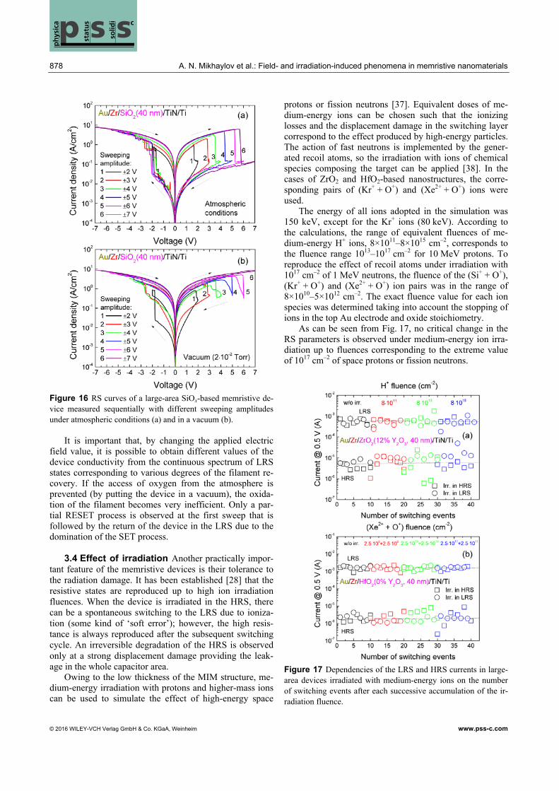
In the case of a SiO2-based memristive device, stable
RS is possible only in atmospheric conditions. Figure 16 presents the RS curves measured sequentially in a cyclic regime with different sweeping amplitudes under atmos-pheric conditions and in vacuum [23].
878 A. N. Mikhaylov et al.: Field- and irradiation-induced phenomena in memristive nanomaterials
© 2016 WILEY-VCH Verlag GmbH & Co. KGaA, Weinheim www.pss-c.com
phys
icap s sst
atus
solid
i c
Figure 16 RS curves of a large-area SiOx-based memristive de-vice measured sequentially with different sweeping amplitudes under atmospheric conditions (a) and in a vacuum (b).
It is important that, by changing the applied electric field value, it is possible to obtain different values of the device conductivity from the continuous spectrum of LRS states corresponding to various degrees of the filament re-covery. If the access of oxygen from the atmosphere is prevented (by putting the device in a vacuum), the oxida-tion of the filament becomes very inefficient. Only a par-tial RESET process is observed at the first sweep that is followed by the return of the device in the LRS due to the domination of the SET process.
3.4 Effect of irradiation Another practically impor-
tant feature of the memristive devices is their tolerance to the radiation damage. It has been established [28] that the resistive states are reproduced up to high ion irradiation fluences. When the device is irradiated in the HRS, there can be a spontaneous switching to the LRS due to ioniza-tion (some kind of ‘soft error’); however, the high resis-tance is always reproduced after the subsequent switching cycle. An irreversible degradation of the HRS is observed only at a strong displacement damage providing the leak-age in the whole capacitor area.
Owing to the low thickness of the MIM structure, me-dium-energy irradiation with protons and higher-mass ions can be used to simulate the effect of high-energy space
protons or fission neutrons [37]. Equivalent doses of me-dium-energy ions can be chosen such that the ionizing losses and the displacement damage in the switching layer correspond to the effect produced by high-energy particles. The action of fast neutrons is implemented by the gener-ated recoil atoms, so the irradiation with ions of chemical species composing the target can be applied [38]. In the cases of ZrO2 and HfO2-based nanostructures, the corre-sponding pairs of (Kr+ + O+) and (Xe2+ + O+) ions were used.
The energy of all ions adopted in the simulation was 150 keV, except for the Kr+ ions (80 keV). According to the calculations, the range of equivalent fluences of me-dium-energy H+ ions, 8×10¹¹–8×1015 cm–2, corresponds to the fluence range 1013–1017 cm–2 for 10 MeV protons. To reproduce the effect of recoil atoms under irradiation with 1017 cm–2 of 1 MeV neutrons, the fluence of the (Si+ + O+), (Kr+ + O+) and (Xe2+ + O+) ion pairs was in the range of 8×10¹⁰–5×1012 cm–2. The exact fluence value for each ion species was determined taking into account the stopping of ions in the top Au electrode and oxide stoichiometry.
As can be seen from Fig. 17, no critical change in the RS parameters is observed under medium-energy ion irra-diation up to fluences corresponding to the extreme value of 1017 cm–2 of space protons or fission neutrons.
Figure 17 Dependencies of the LRS and HRS currents in large-area devices irradiated with medium-energy ions on the number of switching events after each successive accumulation of the ir-radiation fluence.

Phys. Status Solidi C 13, No. 10–12 (2016) 879
www.pss-c.com © 2016 WILEY-VCH Verlag GmbH & Co. KGaA, Weinheim
Invited
Article
The nature of the high radiation tolerance of the mem-ristive devices may be related to the fact that the electric field produces more damage to the oxide material in the nanoscale switching volume than the average damage in-duced by a typical radiation exposure.
3.5 Synaptic behaviour It is worth noting that the
studied memristive devices demonstrate a typical synaptic behaviour of the resistive state [39]. There is a gradual de-pendence of the latter on the width and amplitude of a sin-gle pulse applied to the structure (Fig. 18). One can also see a certain response to the application of repeated identi-cal pulses of different polarity resembling the facilitation and depression phenomena (Fig. 19).
Figure 18 Dependencies of resistance of a large-area SiOx-based memristive device on the width tp (a) and amplitude Vp (b) of a single pulse applied to the structure.
This behaviour allows using our memristive devices in the models of synaptically coupled neuron-like generators (e.g. FitzHugh-Nagumo oscillators). Figure 20 shows the expected change in resistance of a memristive device under the action of a spike-like signal of a certain amplitude that corresponds to an increase in the coupling strength and synchronization of neuron-like generators.
Figure 19 Dependence of the current through a large-area ZrO2(Y)-based memristive device on the number of repeated identical pulses with duration tp and period Tp of different polarity.
Thus, the adaptive behavior of memristive devices, when the coupling strength can be variably depending on the ongoing activity of a neuron-like generator, can pro-vide synaptic plasticity of this coupling. Such neuromor-phic models based on memristive devices can be applied in the design of neurohybrid systems consisting of living neu-rons and electronic control devices.
Figure 20 Scheme of neuron-like generators coupling via a large-area memristive device and oscillograms demonstrating the change of the coupling strength and synchronization due to a de-crease in the memristive device resistance.
At the same time, the memristive device response to a periodic electrical signal is hard to reproduce. There are various thresholds for the change in resistance, and some-

880 A. N. Mikhaylov et al.: Field- and irradiation-induced phenomena in memristive nanomaterials
© 2016 WILEY-VCH Verlag GmbH & Co. KGaA, Weinheim www.pss-c.com
phys
icap s sst
atus
solid
i c
times there is a tendency to sticking in one resistive state. The more complicated pulses are used, the less predictable is the memristive device response. Moreover, it can be said that each memristive device lives its own life, when a complex periodic signal is applied.
3.6 Noise-induced phenomena To understand the
dynamics of a memristive device, it is not sufficient to know in detail the microscopic processes responsible for the RS. Due to the strong space localization of the redox processes responsible for the RS, the generic memristive device should be considered as a multi-stable nonlinear dynamical system driven by a noise and external fields. In these complex macroscopic systems one can observe some interesting and unexpected phenomena with the construc-tive role of noise such as stochastic resonance (see review [40] and references therein), which manifests an enhance-ment of the system response for certain finite values of the noise intensity, noise-enhanced stability of metastable states [41-44], resonant activation [45, 46], etc. Moreover, these effects can be used to control the dynamics of a memristive device.
Several reports [47, 48] have already shown the impor-tance of noise in the response of memristive devices to the external driving field. However, the approach used is lim-ited to the case of a bistable system and must be extended to the multi-stable energetic profile describing the real situation more correctly.
It is important to predict and tailor the reaction of memristive devices to the action of real electrical signals, when trying to couple the memristive devices with biologi-cal cultures and tissues to organize an adaptive interface not only for the processing [49], but also for the classifica-tion and stimulation of the electrical activity of brain cells. There are a new physics and new applications behind such neurointerfaces on the basis of memristive devices.
4 Conclusions Memristive devices are extremely
simple material nanostructures and at the same time very smart and complex nonlinear systems promising a wide range of applications from memory-in-logic to neural net-works and neurointerfaces.
There is a common RS behaviour of the studied mem-ristive devices on the basis of different ionic and covalent oxides determined by the localized (filamentary) redox processes.
The differences in the structure, energetics and insulat-ing properties of the used oxide materials provide the dis-tinctions in quantitative parameters and microscopic mech-anisms responsible for the observed switching peculiarities.
High tolerance of the resistive states to ionizing radia-tion and displacement damage has been demonstrated and is very important for atomic energy and space applications of the developed memristive devices.
The main conclusion from the irradiation study is that the electric field induces such a strong transformation of
the material structure in a local nanoscale volume that there is almost no difference, which oxide is initially used as a switching layer and to which radiation the device is exposed.
Noise-induced phenomena cannot be negligible when considering the memristive device as a nonlinear system and are very important for understanding and tailoring the dynamic response of memristive devices in view of neu-romorphic applications.
Acknowledgements The study was supported by the Rus-sian Science Foundation (16-19-00144). The study of memristive devices at low temperatures (down to liquid helium) with applica-tion of impedance spectroscopy described in Section 3.1 was supported by the FCT of Portugal through the projects and grants UID/CTM/50025/2013, RECI-II/FIS-NAN/0183/2012 (FCOMP-01-0124-FEDER-027494) and PD/BD/105917/2014. The ion-beam simulation approach and experiments described in Section 3.4 were supported by the Ministry of Education and Science of the Russian Federation (3.285.2014/K and RFMEFI57514X0029).
References [1] G. Dearnaley, A.M. Stoneham, and D.V. Morgan, Rep. Prog.
Phys. 33, 1129 (1970). [2] L.O. Chua, IEEE Trans. Cirquit Theory 18, 507 (1971). [3] S. Vongehr and X. Meng, Sci. Rep. 5, 11657 (2015). [4] I. Valov, E. Linn, S. Tappertzhofen, S. Schmelzer, J. van den
Hurk, F. Lentz, and R. Waser, Nature Commun. 4, 1771 (2013).
[5] R. Waser, R. Dittmann, G. Staikov, and K. Szot, Adv. Mater. 21, 2632 (2009).
[6] A. Siemon, T. Breuer, N. Aslam, S. Ferch, W. Kim, J. van den Hurk, V. Rana, S. Hoffmann-Eifert, R. Waser, S. Men-zel, and E. Linn, Adv. Funct. Mater. 25, 6414 (2015).
[7] C. Zamarreno-Ramos, L.A. Camunas-Mesa, J.A. Pérez-Carrasco, T. Masquelier, T. Serrano-Gotarredona, and B. Linares-Barranco, Front. Neurosci. 5, 26 (2011).
[8] S.D. Ha, S. Ramanathan, J. Appl. Phys. 110, 071101 (2011). [9] A. Thomas, J. Phys. D: Appl. Phys. 46, 093001 (2013). [10] D. Kuzum, S. Yu, and H.-S. P.Wong, Nanotechnology 24,
382001 (2013). [11] M.D. Pickett, G. Medeiros-Ribeiro, and R.S. Williams, Na-
ture Mater. 12, 114 (2013), DOI: 10.1038/NMAT3510. [12] A. Mehonic and A.J. Kenyon, Front. Neurosci. 10, 57
(2016). [13] A. Grossi, E. Perez, C. Zambelli, P. Olivo, and C. Wenger,
in: Proc. 2016 Joint International EUROSOI Workshop and International Conference on Ultimate Integration on Silicon (EUROSOI-ULIS), DOI 10.1109/ULIS.2016.7440057.
[14] Y.Y. Chen, M. Komura, R. Degraeve, B. Govoreanu, L. Goux, A. Fantini, N. Raghavan, S. Clima, L. Zhang, A. Belmonte, A. Redolfi, G.S. Kar, G. Groeseneken, D.J. Wouters, and M. Jurczak, IEEE International Electron De-vices Meeting (2013).
[15] T. Breuer, L. Nielen, B. Roesgen, R. Waser, V. Rana, and E. Linn, Sci. Rep. 6, 23967 (2016).
[16] M. Prezioso, F. Merrikh-Bayat, B.D. Hoskins, G.C. Adam, K.K. Likharev, and D.B. Strukov, Nature Lett. 521, 61 (2015).

Phys. Status Solidi C 13, No. 10–12 (2016) 881
www.pss-c.com © 2016 WILEY-VCH Verlag GmbH & Co. KGaA, Weinheim
Invited
Article
[17] V.A. Demin, V.V. Erokhin, A.V. Emelyanov, S. Battistoni, G. Baldi, S. Iannotta, P.K. Kashkarov, and M.V. Kovalchuk, Org. Electron. 25, 16 (2015).
[18] A. Adamatzky and L. Chua (Eds.), Memristor Networks (Springer International Publishing, Switzerland, 2014), p. 720.
[19] D. Ielmini and R. Waser (Eds.), Resistive Switching: From Fundamentals of Nanoionic Redox Processes to Memristive Device Applications (Wiley-VCH, 2016), p. 784.
[20] G. Fuxi and W. Yang (Eds.), Data Storage at the Nanoscale Advances and Applications (Taylor & Francis Group, LLC, USA, 2015), p. 730.
[21] A. Chen, J. Hutchby, V. Zhirnov, and G. Bourianoff (Eds.), Emerging Nanoelectronic Devices (Wiley-VCH, 2015), p. 570.
[22] O.N. Gorshkov, I.N. Antonov, A.I. Belov, A.P. Kasatkin, and A.N. Mikhaylov, Tech. Phys. Lett. 40(2), 101 (2014).
[23] A.N. Mikhaylov, A.I. Belov, D.V. Guseinov, D.S. Korolev, I.N. Antonov, D.V. Efimovykh, S.V. Tikhov, A.P. Kasatkin, O.N. Gorshkov, D.I. Tetelbaum, A.I. Bobrov, N.V. Malek-honova, D.A. Pavlov, E.G. Gryaznov, and A.P. Yatmanov, Mater. Sci. Eng. B 194, 48 (2015).
[24] C.M.M. Rosario, O.N. Gorshkov, A.P. Kasatkin, I.N. An-tonov, D.S. Korolev, A.N. Mikhaylov, and N.A. Sobolev, Vacuum 122, 293 (2015).
[25] D. Kalaev, E. Yalon, and I. Riess, Solid State Ion. 276, 9 (2015).
[26] W. Kim, S. Menzel, D.J. Wouters, Y. Guo, J. Robertson, B. Roesgen, R. Waser, and V. Rana, RCS Nanoscale, in press, DOI: 10.1039/c6nr03810g (2016).
[27] S.V. Tikhov, O.N. Gorshkov, I.N. Antonov, A.P. Kasatkin, D.S. Korolev, A.I. Belov, A.N. Mikhaylov, and D.I. Te-tel’baum, Tech. Phys. 61, 745 (2016).
[28] A.I. Belov, A.N. Mikhaylov, D.S. Korolev, V.A. Sergeev, I.N. Antonov, O.N. Gorshkov, and D.I. Tetelbaum, Tech. Phys. Lett. 42, 505 (2016).
[29] A. Fantini, D.J. Wouters, R. Degraeve, L. Goux, L. Pan-tisano, G. Kar, Y.-Y. Chen, B. Govoreanu, J.A. Kittl, L. Al-timime, and M. Jurczak, IEEE International Memory Work-shop (2012).
[30] D. Guseinov, D.I. Tetelbaum, A.N. Mikhaylov, A.I. Belov, M.E. Shenina, D.S. Korolev, I.N. Antonov, A.P. Kasatkin, O.N. Gorshkov, E.V. Okulich, V.I. Okulich, A.I. Bobrov, N.V. Malekhonova, D.A. Pavlov, and E.G. Gryaznov, Int. J. Nanotechnology (2016), in press.
[31] O. Gorshkov, A.N. Mikhaylov, A.P. Kasatkin, S.V. Tikhov, D.O. Filatov, D.A. Pavlov, A.I. Belov, M.N. Koryazhkina, A.I. Bobrov, N.V. Malekhonova, E.G. Gryaznov, I.N. An-tonov, and M.E. Shenina, J. Phys. Conf. Ser. (2016), in press.
[32] N.F. Mott and E.A. Davis, Electron Processes in Non-Crystalline Materials (Clarendon Press, Oxford, 1979).
[33] J. Yao, L. Zhong, D. Natelson, and J.M. Tour, Sci. Rep. 2, 242 (2012).
[34] Y. Matveyev, R. Kirtaev, A. Fetisova, S. Zakharchenko, D. Negrov, and A. Zenkevich, Nanoscale Res. Lett. 11, 147 (2016).
[35] S. Menzel, U. Böttger, M. Wimmer, and M. Salinga, Adv. Funct. Mater. 25, 6308 (2015).
[36] L. Goux, P. Czarnecki, Y.Y. Chen, L. Pantisano, X.P. Wang, R. Degraeve, B. Govoreanu, M. Jurczak, D.J. Wouters, and L. Altimime, Appl. Phys. Lett. 97, 243509 (2010).
[37] D.I. Tetelbaum, D.V. Guseinov, V.K. Vasiliev, A.N. Mik-haylov, A.I. Belov, D.S. Korolev, S.V. Obolensky, and A.N. Kachemtsev, Nucl. Instrum. Methods B 326, 41 (2014).
[38] A. Belov, A. Mikhaylov, D. Korolev, D. Guseinov, E. Gryaznov, E. Okulich, V. Sergeev, I. Antonov, A. Kasatkin, O. Gorshkov, D. Tetelbaum, and V. Kozlovski, Nucl. In-strum. Methods B 379, 13 (2016).
[39] D.S. Korolev, A.N. Mikhaylov, A.I. Belov, V.A. Sergeev, I.N. Antonov, O.N. Gorshkov, and D.I. Tetelbaum, J. Phys. Conf. Ser. (2016), in press.
[40] L. Gammaitoni, P. Hänggi, P. Jung, and F. Marchesoni, Rev. Mod. Phys. 70, 223 (1998).
[41] I. Dayan, M. Gitterman, and G. H. Weiss, Phys. Rev. A 46, 757 (1992).
[42] R.N. Mantegna and B. Spagnolo, Phys. Rev. Lett. 76, 563 (1996).
[43] N.V. Agudov, Phys. Rev. E 57, 2618 (1998). [44] A.A. Dubkov, N.V. Agudov, and B. Spagnolo, Phys. Rev.
E 69, 061103 (2004). [45] C.R. Doering and J.C. Gadoua, Phys. Rev. Lett. 69, 2318
(1992). [46] R.N. Mantegna and B. Spagnolo, Phys. Rev. Lett. 84, 3025
(2000). [47] A. Stotland and M. Di Ventra, Phys. Rev. E 85, 011116
(2012). [48] G.A. Patterson, P.I. Fierens, and D.F. Grosz, Appl. Phys.
Lett. 103, 074102 (2013). [49] I. Gupta, A. Serb, A. Khiat, R. Zeitler, S. Vassanelli, and T.
Prodromakis, arXiv 1507.06832v1 (2015).