Embed Size (px)
Citation preview

105
4Spintronic Device Memristive Effects and Magnetization Switching Optimizing
Xiaobin WangAvalanche Technology, Fremont, California
4.1 Introduction
Spintronics, an exploration of spin properties instead of or in addition to charge degrees of freedom, holds promise to continue device miniaturiza-tion in the postsilicon era and beyond the age of Moore’s law. The benefits of spintronics come from the fact that there is no need for electric current to retain spin, and there are many paths to change spin without massively moving electrons.
CONTENTS
4.1 Introduction ................................................................................................ 1054.2 Spintronic Device Memristive Effects .................................................... 107
4.2.1 Spin Torque Device Read and Write Dynamics ........................ 1074.2.2 Spintronic Device Memristive Effects ........................................ 112
4.3 Potential Application of Spintronic Memristive Effects ....................... 1144.4 Spintronic Device Writing Optimizing .................................................. 121
4.4.1 Fastest Magnetization Switching with Minimum Joule Heating ............................................................................................ 121
4.4.2 Minimum Heat Dissipation Intrinsic to Magnetization Reversal ........................................................................................... 125
4.4.3 Effects of Polarization Direction and Precessional Magnetiation Switching ................................................................ 128
4.5 Spintronic Device Reading Operation Memristive Effects .................. 1374.6 Conclusion .................................................................................................. 142References ............................................................................................................. 143
Copyrighted Material - Taylor and Francis

106 Metallic Spintronic Devices
While full of fundamental challenges, spintronics technology has been tested in existing applications, such as magnetic data storage devices and field-driven magnetic random access memory (MRAM). Emerging spin-tronics applications, such as spin torque random access memory (SPRAM), spin-based logic, spin transistors, and spin quantum computer, are currently under extensive research and development. For example, SPRAM is an emerging technology that integrates magnetic tunneling junction (MTJ) and complementary metal oxide semiconductor (CMOS) to achieve nonvolatil-ity, fast writing/reading speed, almost unlimited programming endurance, and zero standby power. As charge-based memory technologies such as dynamic random access memory (DRAM) or NAND Flash are facing severe scalability problems due to precise charge placement and sensing hurdles in deep-submicron processes, SPRAM is widely believed in industry to be a candidate to replace charge-based memory. A recent announcement of the first commercial SPRAM (Everspin, November 2012) and continuing dem-onstration of SPRAM scalability (down to the 54 nm technology node) have confirmed the viability of the SPRAM technology path.
Electric field- or voltage-induced magnetization switching provides an exciting opportunity for switching magnetization without resorting to elec-tronic transport across the device. It has been demonstrated both experimen-tally and theoretically that electric fields can manipulate magnetic anisotropy to induce magnetization switching. Another electric field-induced magneti-zation switching system is multiferroics, which has coupled magnetic and ferroelectric order parameters. When applied to practical devices, electric field-induced magnetization switching can lead to low-power magnetization switching with very little heat generation.
Another intensively investigated approach to switch magnetization is with ultra-fast light pulse. It is generally believed that ultra-fast laser pulse could either rapidly heat the spin system to Curie temperature for easy magneti-zation switching or induce an inverse Faraday effect to switch magnetiza-tion effectively. One of the advantages of laser pulse-induced magnetization switching is the extremely fast magnetization switching speed. Magnetization speeds down to the picosecond level have been reported utilizing this switch-ing mechanism.
The modern nanoscale spintronic device has reached a stage where device performance is explicitly determined by coupling between macroscopic magnetization dynamics, microscopic spin electron transport, and finite temperature thermal agitations. An ever-increasing challenge is to achieve well-controlled faster magnetization switching and maintain stable magne-tization states at longer timescales at higher temperatures. A coupled, multi-scale dynamic approach considering both device mean performance and its variance is required for spintronic devices’ understanding and design.
Memristive effects are universal for spin torque spintronic devices at the timescale that explicitly involves the interactions between magnetiza-tion dynamics and electronic charge transport. In this chapter, we explore
Copyrighted Material - Taylor and Francis

107Memristive Effects and Magnetization Switching Optimizing
spintronic device memristive effects through stochastic magnetization dynamics. Although memristive effects provide many exciting new applica-tion possibilities for spintronic devices, they also have quite strict constraints on spintronic device operations, such as writing speed and heat dissipation. We will explore spintronic device write and read optimization in light of spintronic memristive effects.
4.2 Spintronic Device Memristive Effects
4.2.1 Spin Torque Device Read and Write Dynamics
The giant magnetoresistive (GMR) effect was the key physical principle for commercial magnetic hard disk drive read sensors, for which the Nobel Prize in Physics was awarded to Peter Grunberg and Albert Fert. In GMR devices, two ferromagnetic layers sandwich a nonferromagnetic metal known as a spin valve structure. Spin valve resistance depends on the relative mag-netic orientations of the two ferromagnetic layers. Device resistance is low when the magnetizations of two ferromagnetic layers are parallel, and device resistance is high when the magnetizations of two ferromagnetic layers are antiparallel. A GMR-based spin valve has a dramatically increased hard disk drive areal density through its excellent sensitivity for magnetic flux. Recently the GRM structure has been replaced by the tunneling magnetore-sistance (TMR) structure. The TMR device has two ferromagnetic layers that sandwich a tunneling-insulating barrier known as the magnetic tunneling junction (MTJ). Similar to the spin valve, MTJ resistance is low when the mag-netizations of two ferromagnetic layers are parallel, and device resistance is high when the magnetizations of two ferromagnetic layers are antiparallel. Compared to GMR, TMR has a much higher value of resistance difference over resistance. The TMR value, which is usually defined as the difference between high resistance and low resistance divided by low resistance, is around 100% in commercial sensors and could reach 600 to 1000% in the lab.
The key physics principle behind GMR and TMR sensing operations is the resistance dependence upon magnetization states. It can be written as
θ = + − − θG G G G G( )2 2
cosP AP AP P (4.1)
where GP , GAP are the conductances for free layer magnetization parallel and antiparallel to reference layer magnetization. θ is the angle between free layer magnetization and reference layer magnetization.
For magnetic random access memory, besides providing a sensing scheme based upon magnetization state-dependent resistance, a spin valve or MTJ
Copyrighted Material - Taylor and Francis

108 Metallic Spintronic Devices
structure also stores magnetic information. Magnetic tunneling junction (MTJ) is the key component of spin torque random access memory (SPRAM) cell. Figure 4.1 shows a schematic picture of MTJ-based SPRAM. Two ferromagnetic layers sandwich an oxide barrier layer, for example, MgO. The magnetization direction of one ferromagnetic layer (reference layer) is fixed by coupling to a pinned magnetization layer above, while the magnetization direction of the other ferromagnetic layer (free layer) can be changed. The 0/1 data information is stored as the magnetization direction of the free layer in SPRAM.
The writing operation of SPRAM is based upon spin polarization current-induced magnetization switching [1, 2]. To switch the free layer magnetiza-tion to the same direction of the reference layer magnetization, an electric current passes from the reference layer to the free layer. The injected current electrons have spins pointing to the same and opposite directions of the ref-erence layer magnetization. After passing through the reference layer, the electrons have a preferred spin orientation direction pointing to the same direction of the reference layer magnetization. This is because most of the electrons with spin pointing to the opposite direction of the reference layer magnetization are reflected back due to interaction between the itinerant electron spin and the reference layer local magnetization. The polarized cur-rent electrons, with a net spin moment in the same direction as the reference layer magnetization, will switch the free layer magnetization to the same direction as the reference layer magnetization.
In order to switch the free layer magnetization to the opposite direction of the reference layer magnetization, electron current passes from the free layer to the reference layer. Based upon the same physics argument as before, the reflected electrons from the reference layer have preferred spin direction opposite to the direction of the reference layer magnetization. These will switch the free layer magnetization to the opposite direction of the reference layer magnetization.
The key physical principle behind MTJ writing is that the free layer mac-roscopic magnetization states are changed by the torque provided through spin current. This is a complex dynamic process described by the stochastic
Current Driving Spin Torque Magnetic Random Access Memory (SPRAM)
SelectTransistor
Free layer
Reference layer
Magnetictunneling junction(MTJ)
Tunneling insulatingbarrier
Bottom electrode
MTJ
Top electrode
FIGURE 4.1Schematic pictures of structure and working principle of spin torque random access memory. (From X. Wang et al., CMOS Processors and Memories, Springer, Berlin, 2010. With permission.)Copyrighted Material - Taylor and Francis

109Memristive Effects and Magnetization Switching Optimizing
Landau-Lifshitz-Gilbert equation at a finite temperature with spin torque terms:
= − × + − α × × + +
� � � � � � � ��
dmdt
m h h m m h h TM
( ) ( )eff th eff ths (4.2)
where �m is the normalized magnetization vector, and time t is normalized
by γ Ms , with γ being the gyromagnetic ratio and Ms being the magnetization saturation.
= = ∂ε∂
� ��h H Mm
/eff eff s
is the normalized effective magnetic field with normalized energy density ε, and α is the damping parameter.
�hfluc is the thermal fluctuation field, whose
magnitude is determined by the fluctuation-dissipation condition at room temperature and whose formalism follows reference [3].
=�
�T T
M Vnorms
is the normalized spin torque term with units of magnetic field. The net spin torque
�T can be obtained through the microscopic quantum electronic spin
transport model [4–11]. At the macroscopic magnetization dynamics level, spin torque can be approximated through an adiabatic term proportional to
× ×� � �m m p and a nonadiabatic term proportional to ×
� �m p, where �p is a unit
vector pointing to the spin polarization direction.Let’s consider a MTJ free layer element with a perpendicular uniaxial
anisotropy energy ε = θ(sin )/ 22 , where θ is the angle between magnetiza-tion orientation and anisotropy axis. The magnetic energy is normalized by MsHkV, with Hk being the magnetic anisotropy, Ms being the magnetic saturation, and V being the element volume. Magnetization dynamics based upon the stochastic Landau-Lifshitz-Gilbert equation with the Berger and Slonczewski spin torque term (4.2) in this case can be written as [12]
θ = − ∂ε
∂θ+ θ +δ θ + δ
= − θ θ + θ +δ θ + δ
d dt h dt ctg dt dB
dt h dt ctg dt dB
sin 2
sin cos sin 2
(4.3)
where time is normalized by αγHk, with γ being the gyromagnetic ratio and α the damping parameter. h is the effective field whose magnitude is propor-tional to the spin current magnitude.
Copyrighted Material - Taylor and Francis

110 Metallic Spintronic Devices
δ = k T
H M VB
k s
is the thermal energy over magnetic energy. kBT is the Boltzmann thermal factor. dB in Equation (4.3) represents Brownian motion increment.
The current magnitude required to switch free layer magnetization is a dynamic concept. Although we talk about the critical switching current hcr , which is the minimum current magnitude achieving { })(θ − θ ≥hinf sin cos 0
h
for all magnetization angles θ, magnetization switching could happen at any current magnitude due to the combined spin torque dynamics and random thermal fluctuations. An example of current magnitude versus switching time is shown in Figure 4.2. This curve shows the spin torque-induced mag-netization switching in the whole time range, from short-time dynamical switching to long-time thermal switching. Besides fast dynamical magnetiza-tion switching induced by a spin current with a magnitude bigger than that of the critical switching current, magnetization switching also occurs in the thermal switching region where spin current magnitude is lower than critical switching current. This curve shows one of the fundamental challenges of spin torque devices, that is, how to achieve fast nanosecond dynamic magne-tization switching and at the same time maintain long-time thermal stability at second-to-year scales.
The critical switching current for Equation (4.3) is hcr = 1 according to { })(θ − θ ≥hinf sin cos 0
h. For dynamical switching with current amplitude
0–1–2–3–4Log 10 (time (sec))
Switc
hing
Cur
rent
Den
sity (
MA
/cm
2 )
Square: Measurement
Spin torque switching
Curve: Model
–5–6–7–8–90
1.7
3.4
5.1
6.9
8.6
10
12
FIGURE 4.2Dynamic thermal switching of magnetic elements with spin torque current. Squares are exper-iment data and curves are theoretical calculations. (From X. Wang et al. IEEE Trans. Magn., 45, 2039, 2009. With permission.)
Copyrighted Material - Taylor and Francis

111Memristive Effects and Magnetization Switching Optimizing
bigger than that for the critical switching current, h > 1, the following asymp-totic solution of Equation (4.3) can be obtained for current pulse duration versus current amplitude based upon δ << 1. δ << 1 holds true for a stable magnetic device with magnetic energy bigger than thermal energy at finite temperature:
( )
θ δ = + θ − + θ + −− +
− θ − δ + θ − δ + γ−
+θ−
−− +
+ − δ−
+ γ−
T h h h hh h
h Ei hh h
hh h
hh h
( , , ) ( 1) ln[tan( /2)] ln[( 1) tan( /2) ( 1)]( 1)( 1)
ln[ ( 1)/(2 )] [ ( 1)/(2 )]/2 /21
ln1
ln(2 )( 1)( 1)
ln[ ( 1)/(2 )]1 2( 1)
2
2 (4.4)
Equation (4.4) is the average time duration T required for a constant ampli-tude current h to drive magnetization starting at angle θ to the magnetiza-tion switching at saddle position.
∫ ∫θ = θ θ θ θ θ− θ δ − θ δe d e d( sin )/( sin )sin /2 sin /22 2
Figure 4.3 shows current pulse magnitude versus inverse of current pulse duration for devices with different thermal stabilities. The magnetization initial angle is determined by the Boltzmann distribution at equilibrium: θ. Linear dependence of current amplitude upon the inverse of current
1.61.41.210.80.60.40.21
1.5
2.5
3.5
3
4
2
�ree curves from top tobottom correspond toδ = 120, 100, 80
Inverse of Current Pulse Duration
Curr
ent P
ulse
Am
plitu
de
FIGURE 4.3Spin torque current magnitude versus inverse of the pulse duration to achieve MTJ magnetiza-tion switching.
Copyrighted Material - Taylor and Francis

112 Metallic Spintronic Devices
duration is observed. Figure 4.3 shows clearly that in order to achieve fast magnetization switching, a sufficient amount of the charge (which is pro-portional current amplitude multiplied by current duration) is required to flow through the MTJ device. It is the time integration of the current, instead of current amplitude, that determines the MTJ magnetization final state. Because MTJ resistance depends upon the magnetization state, as in Equation (4.1), the MTJ final resistance state depends upon the charge pass-ing through the device.
4.2.2 Spintronic Device Memristive Effects
A device with resistance dependence upon charge or current integration was proposed as a memristor in [13]. The original definition of memristor was
dϕ = Mdq (4.5)
where q is the electric charge, ϕ is the magnetic flux, and M is the mem-ristance. Because magnetic flux is the integration of voltage and charge is the integration of current, it is easy to show that
= φ =M q d dtdq dt
VI
( ) //
(4.6)
What makes memristance different from an ordinary constant resistance or even a current- or voltage-dependent nonlinear resistance is that mem-ristance is a function of charge, which depends upon the hysteretic behavior of the current (or voltage) profile. The above definition of memresistor can be generalized to a memristive system:
=
=
V M m i
dmdt
f i m
( )
( , ) (4.7)
where m is an implicit state variable, such as charge, that depends upon the integration of the current profile over time. In the spintronic memristor here, m can be the magnetization state. Although the unit of memristance is the same as that of resistance (ohm), the intrinsic constitution relation for the memristor is quite different from three other well-known circuit elements: resistance (R), capacitance (C), and inductance (L). The intrinsic constitution relation for the memristor is charge versus flux. Thus, the memristor has the unique ability to accumulate current/voltage information through constant current or voltage driving strength. As a comparison, in order to keep accu-mulating charge, the capacitor must be driven with a varying voltage. This
Copyrighted Material - Taylor and Francis
113Memristive Effects and Magnetization Switching Optimizing
is because the intrinsic constitution relation of the capacitor is charge versus voltage. Because of its unique intrinsic constitution, the memristor is also called the fourth element of the circuit.
It has been shown in [14] that memristive effects are universal for spin torque spintronic devices at the timescale that explicitly involves the interactions between magnetization dynamics and electronic charge transport. For spin torque devices, the device resistance depends upon its magnetization state. The magnetization state of the device depends upon the cumulative effects of electron spin excitations. Thus, a spin torque spintronic device is a spin-tronics memristor with its resistance dependent upon the integral effects of its current profile.
Another example of a spintronic memristor is the spintronic domain wall device. The device structure is shown in Figure 4.4. It consists of a long spin valve strip that includes two ferromagnetic layers: the reference layer and free layer. The magnetization direction of the reference layer is fixed by coupling to a pinned magnetic reference layer. The free layer is divided by a domain wall into two segments that have opposite magnetization direc-tions to each other. The device domain resistance depends upon the domain wall position as
= − −
R X RD
R R X tD
( ) ( ) ( )H H L (4.8)
where RH and RL are the high and low resistance of the spin valve, D is the spin valve length, and X(t) is the domain wall position. The free layer mag-netization dynamics can be described by the stochastic Landau-Lifshitz-Gilbert equation using rigid wall approximation [15, 16]:
D
x
Pinned reference layer
A
Domain wall motion in free layer
x
yz
h
w
z
FIGURE 4.4Spin valve with domain.
Copyrighted Material - Taylor and Francis

114 Metallic Spintronic Devices
�
+ α = β + γ +η
−α = ω + +η
η η ′ = η η ′ = α δ − ′
ddt w
dXdt
vw
H
wdXdt
ddt
vw
t t t t k TN
t t
1 sin(2 )
( ) ( ) ( ) ( ) 2 ( )
s
sX
X XB
0 (4.9)
The domain wall motion is expressed in terms of magnetization spherical angle θ, φ as θ = θ −x t x X t( , ) ( ( ))0 , ϕ = ϕx t t( , ) ( )0 . The magnetiza-tion vector is θ ϕ θ ϕ θM (sin cos , sin sin , cos )s . The domain wall shape is
θ =x x wcos ( ) tanh( / )0 with a wall length =w A M H2 / s k . The wall length is determined by Ms exchange strength A, and easy-axis anisotropy Hk in the x-direction. ω = γH / 2p0 , with γ being the gyromagnetic ratio and Hp being a hard y plane anisotropy. =v PJu eM/s B s is the spin torque excitation strength. Spin torque excitation strength is proportional to current density J. uB is the Bohr magneton and e is the elementary electron charge. P is the polarization efficiency, which can be approximate as
= σ − σσ + σ
↑ ↓
↑ ↓P
for two spin channel models with spin-up and -down conductivity σ↑ ↓, . H is the effective magnetic field. β is the ratio of nonadiabatic spin torque strength to adiabatic spin torque strength.
Figure 4.5 shows the inverse of current pulse duration versus current pulse amplitude for a domain wall to travel a fixed distance. The inverse of the current pulse is normalized by vs /w. The current pulse amplitude is nor-malized by PJuB /eMswω0, and the temperature is normalized by 4kBT/Nħω0. The fixed distance is 1 (normalized by w). The inverse of the current pulse duration depends almost linearly upon the current pulse amplitude for a wide range of temperatures. For the spin torque domain wall device, it is the charge instead of current magnitude that determines the final domain wall position and the device resistance. For the domain wall device, a continuum of resistance states can be explored through moving the domain wall across the thin-film structure.
4.3 Potential Application of Spintronic Memristive Effects
After proposing resistive memory switching in the metal-insulator-metal struc-ture as nanoscale memristors [17], there is a burst of interest in the potential
Copyrighted Material - Taylor and Francis

115Memristive Effects and Magnetization Switching Optimizing
application of nanoscale memristors. It is also shown that the majority of mem-ory material-based two-terminal electronic devices behave as memristors or a combination of memristors, memcapacitors, and meminductors when sub-jected to time-dependent perturbations [18]. Thus, it is no surprise that there are many potential applications of spintronic memristive effects.
Random access memory is the most obvious application of memristive systems. For spin torque random access memory, one may ask why it is necessary to examine spin torque-induced magnetization switching from a memristive point of view. The benefit of investigating memristive effects on spin torque random access memory can be illustrated through switching of a multicell SPRAM. It was shown [19] that memristive effects of magnetization switching provide additional freedom for us to manipulate magnetization switching between multiple equilibrium states.
MTJ multilevel cell spin torque switching has been demonstrated experi-mentally in [20]. Two multibit MTJ cell examples are presented. In the first example, two horizontal domains are introduced in the MTJ free layer to generate four bits: 00/01/10/11. In the second example, two MTJs are stacked vertically to generate four bits. Figure 4.6 shows schematically the switching behavior of these multibit MTJ cells through the R-I curve. One bit of the two-bit cell is hard and requires higher current to switch, and the other bit is soft and requires less current to switch. Thus, by varying switching current magnitude, individual bits can be switched. In the following we denote the first bit as the hard bit and the second bit as the soft bit.
1.041.020.980.960.940.920
0.05
0.1
0.2
0.3
0.15
Inve
rse o
f Pul
se D
urat
ion
0.25
0.35
1
Current Pulse Amplitude
Normalized thermalfluctuation magnitudefrom 0.008 to 0.012
FIGURE 4.5Inverse of current pulse duration versus pulse amplitude for a domain wall to move a given distance at different temperatures. (From X. Wang et al., IEEE Device Lett. 31, 20, 2010. With permission.)
Copyrighted Material - Taylor and Francis

116 Metallic Spintronic Devices
Based upon R-I curve switching behavior, a multibit MTJ cell has revers-ible branches and irreversible branches. For example, reversible transitions between 11 and 10, 01 and 00 can be achieved; however, the 00 state cannot be directly switched to the 10 state using a single current pulse because switch-ing the first bit requires higher current than switching the second bit.
MTJ memristive effects provide an approach to design a two-bit MTJ cell with reversible switching for all bit combinations. As illustrated in the previ-ous section, spin torque-excited MTJ is a memristor. When the observation time reaches a scale that explicitly involves interactions between magnetiza-tion dynamics and electronics transport, the I-V curve (or widely used R-I curve) is not intrinsic to MTJ. MTJ resistance switching is determined by the current/voltage profile. MTJ switching behavior is determined by integra-tion of the current pulse instead of the current magnitude itself.
Two curves in Figure 4.7 correspond to two MTJ subcells with the same material. The two cells have different shape-induced anisotropy and effec-tive volume. The dot line subcell has a more square shape and bigger surface area, while the square curve has a more elongated shape and less surface area. The elongated subcell requires less current to switch at a smaller cur-rent magnitude; however, the switching speed of the elongated subcell is slower than that of the squared cell when the current magnitude increases. As a result, two switching curves cross at a current magnitude of around 900 µA and pulse width of around 4 ns. If we denote the elongated subcell as a soft bit, the two subcells of MTJ can be switched freely by using currents with different pulse widths. The longer current pulse width switches the soft subcell, corresponding to switching between 00 and 01 states. The shorter current pulse width switches the hard subcell, corresponding to switching between 00 and 10 states.
It is well known that a memristor has rich dynamic behavior when excited with a dynamic current/voltage profile. The example here shows a practi-cal application in multibit MTJ cell switching. By controlling the switching
Current
Resis
tanc
e
11
10
01
00
FIGURE 4.6Multibit MTJ cell resistance versus current. (From X. Wang and Y. Chen, in Design, Automation and Test Conference in Europe, 2010, IEEE 10.1109/DATE.2010.5457118. With permission.)
Copyrighted Material - Taylor and Francis

117Memristive Effects and Magnetization Switching Optimizing
current pulse width, the subcells of MTJ are designed to switch freely between different bit combinations. What is illustrated here is that memristive effects of magnetization switching provide additional freedom to manipulate mag-netization switching.
Crossbar architecture was investigated intensively on resistive memory structure [21]. Compared to conventional memory structure, cross-point design could relax the density limitation of two terminal devices imposed by the CMOS circuit, thus offering a significant improvement in achievable den-sity. Similar architecture was proposed for spin torque devices and MRAM structures [22]. Other areas of memristor digital applications include logic [23], field-programmable gate arrays (FPGAs) [24], image processing [25], etc. It would be interesting to see future spintronic devices penetrate into these technology applications.
A nonvolatile full adder based on logic-in-memory architecture was fab-ricated using magnetic tunnel junctions (MTJs) in combination with metal oxide semiconductor (MOS) transistors [26]. MTJs are used for TMR read and spin torque magnetization switching write. The MOS transistors are fabri-cated using a complementary metal oxide semiconductor (CMOS) process. The basic operation of the full adder was demonstrated. An all-function-in-one magnetic chip reconfigurable logic device was proposed based upon an MTJ stack with spin torque magnetization [27].
Race track memory [28] consisting of three-dimensional ferromagnetic nanowires that are encoded with domain walls has been proposed to achieve large storage capability and fast write read speed. Spin torque-induced
2.5
Switch00 -> 10
Switch00 -> 01
3 × 10821.50.500
200
400
600
800
1000
1200Sw
itchi
ng C
urre
nt (u
A)
1400
1Inverse of Pulse Width (sec–1)
FIGURE 4.7Switching current versus inverse pulse width for two multibit MTJ subcells’ pulse magnitude versus duration for moving domain wall to a given distance. (From X. Wang and Y. Chen, in Design, Automation and Test Conference in Europe, 2010, IEEE 10.1109/DATE.2010.5457118. With permission.)
Copyrighted Material - Taylor and Francis

118 Metallic Spintronic Devices
domain wall motion coherently transports the domain wall along the wire to pass read and write devices. This device structure not only eliminates mechanical moving parts in the current hard disk drive, but also has the capability to be real three-dimensional. Depending upon the number of domains per track, race track memory can achieve very high areal density, replacing the hard disk drive. Depending upon spin torque domain wall motion control, race track memory can achieve very high speed, encroach-ing logic device applications.
Similar to the question asked for spin torque-induced magnetization switching, we may ask the benefit of examining memristive effects in spin torque-induced domain wall motion. Here we answer this question through a spintronic memristor temperature sensor example [29]. The proposed device has the same structure as that shown in Figure 4.4. It operates in a region where device electric behavior is sensitive to temperature change. This is achieved through a combination of temperature-dependent domain wall mobility and positive feedback between resistance and driving strength in the memristor.
A biasing voltage pulse with constant magnitude is applied to the spin-tronic memristor. Resistances before and after voltage pulse are measured. This resistance difference is calibrated to sense temperature magnitude. Solid curves in Figure 4.8 show the resistance as a function of current pulse duration at different temperatures. Positive feedback between the resistance and domain wall driving strengths is critical in the observed high sensitivity in Figure 4.8.
1201008060
400 K
350 K
300 K
Time (nsec)40200
540
550
560
570
580
590
600
Resis
tanc
e (O
hm)
610
620
FIGURE 4.8Spintronic memristor resistance as a function of time at different temperatures for a constant magnitude voltage pulse driving. (From X. Wang et al., IEEE Device Lett. 31, 20, 2010. With permission.)
Copyrighted Material - Taylor and Francis

119Memristive Effects and Magnetization Switching Optimizing
The positive feedback between resistance and driving strength is a unique property of the memrisor. Memristor’s resistance depends upon the inte-gration of current/voltage excitation. For a constant voltage pulse driving, higher temperature results in an increased domain wall moving distance. The increased domain wall moving distance results in a smaller resistance. The smaller resistance results in a higher driving current density, thus pro-viding positive feedback to further increase domain wall distance. This posi-tive feedback accelerates domain wall speed and reduces device resistance further for constant voltage pulse driving.
For a comparison, dash curves in Figure 4.8 are resistance change for non-memristive devices without positive feedback between resistance change and driving strength. The dash curve is generated with a fixed domain wall driving strength.
For the device design example in Figure 4.8, the material properties are mag-netization saturation Ms = 1010 emu/cc, exchange strength A = 1.8 ⋅ 10–11 J / m, easy z-axis anisotropy Hk = 100 Oe, and hard y-axis anisotropy Hp = 5000 Oe. The resistance of square thin film is 50 Ω for 70 Å thickness square thin film, and GMR is 12%. The geometry of the device is 268 nm long, 10 nm wide, and 1.7 nm thick. The damping parameter is α = 0.02 and polarization efficiency is P = 0.3. The number of spins in the domain wall is N = 2.2 ⋅ 107. Based upon the above parameters, the normalized thermal magnitude is
ω =�k T N4 / 0.008B 0 at room temperature T = 300 K. The normalized current driving strength is ω =PJu eM w/ 0.9B s 0 at J 2.75 10 A/cm8 2= ⋅ . A constant 0.3 V voltage pulse with 80 ns duration is applied to the device.
It should be pointed out that the proposed device requires much lower power supply voltage and power consumption compared to the available on-chip temperature sensor. The device could target the highly integrated on-chip thermal detection application, different from many of the stand-alone or bulk thermal sensors.
The feedback between resistance and integrated current or voltage in the memristor provides opportunities for power monitoring and control. Connecting a memristor with a very small resistance could monitor cir-cuit power consumption. This is because the memristor has the ability to accumulate current/voltage through constant current or voltage driving strength. For active circuit power control, instead of a positive feedback between decreasing resistance and increasing domain wall driving strength for a domain wall moving in a direction to reduce resistance, we can design a spintronic device with a negative feedback between resistance and domain wall driving strength for a domain wall moving in a direction to increase resistance. When the circuit power increases, the memristor domain wall is pushed toward a direction to increase the memristor resistance. For mem-ristor resistance comparable to that of the circuit, this reduces the current and power through the circuit. Again, all these spintronic memristor appli-cations could target highly integrated on-chip due to the mature integration between magnetic MTJ and CMOS circuits.
Copyrighted Material - Taylor and Francis

120 Metallic Spintronic Devices
Analog and analog-digital mixture are important areas for memristor application. Neural computing and various learning algorithms are typical examples. Self-organized computation with unreliable memristive nanode-vices were shown in [30]. Analog applications explore the continuous states of the memristive devices. Massively parallel computing architecture based upon a memristive system was shown to be able to solve a maze problem faster than current existing algorithms [31]. Other examples include fuzzy logic [32, 33], adaptive filter [34], chaotic circuits [35], etc.
Utilizing memristors as artificial synapses to efficiently realize some basic functions of the brain is an interesting topic. A design scheme is proposed for ultra-low-power neuromorphic hardware with a spin-based device for neurons [36]. Spin neurons are lateral spin valves and domain wall magnets that operate at ultra-low voltage. MTJs are employed for interfacing the spin neurons with charge-based devices, like CMOS, for large-scale networks. The “brain in a box” concept was proposed based upon spintronic devices [37]. The stochastic nature of spin torque switching of MTJs was utilized to implement spike timing-dependent plasticity of synapses. An experimental and theoretical study of MTJ magnetization switching mean and variance was given in [38], and their implications to SPRAM scaling down were pre-sented in [39]. Figures 4.9 and 4.10 show measured and modeled MTJ switch-ing mean and variations at different pulse durations.
0–1–2
Square: MeasurementCurve: Model
–3–4Log 10 (time (sec))–5
Switc
hing
Cur
rent
Sta
ndar
d D
evia
tion
(uA
)
–6–7–85
10
15
20
25
30
35
FIGURE 4.9Switching current density standard deviation versus mean switching time. The mean switch-ing current density is shown in Figure 4.2. (From X. Wang et al., IEEE Trans. Magn. 45, 2038, 2009. With permission.)
Copyrighted Material - Taylor and Francis

121Memristive Effects and Magnetization Switching Optimizing
4.4 Spintronic Device Writing Optimizing
Although spintronic memristive effects provide many exciting new applica-tion possibilities, they also have a strict constraint on spintronic device writ-ing speed. Spintronic memristive effects state that the device writing speed is roughly proportional to current magnitude because a fixed amount of the charge is required to pass through the device to change its state. Another consequence is that Joule heating during device writing is proportional to its operation speed. This is because Joule heating is proportional to charge multiplying voltage. For the requirement of a given amount of the charge to switch the device, the Joule heating is proportional to current, which is pro-portional to the switching speed.
4.4.1 Fastest Magnetization Switching with Minimum Joule Heating
Because a memristive device’s behavior depends upon time-dependent cur-rent or voltage profile, in order to relieve memristive effects’ constraint on device performance, we first optimize the electric voltage profile and magne-tization dynamics to achieve the fastest magnetization speed with the small-est Joule heating.
We consider the magnetization switching mode in Equation (4.3) corre-sponding to an MTJ free layer element with a perpendicular uniaxial
Switc
hing
Tim
e std
/Sw
itchi
ng T
ime M
ean
–5 –4 –3 –2 –1 0–5
–4.5
–4
–3.5
–3
–2.5
–2
–1.5
–1
–0.5
0
Log 10 (Mean switching time (sec))
Log
10 (S
td o
f sw
itchi
ng ti
me (
sec)
) Experiment1
0.9
0.8
0.7
0.6
0.5
0.4
–7 –6 –5 –4 –3 –2 –1 0Log 10 (Time (sec))
Model
FIGURE 4.10Modeled and measured switching time standard deviation as a function of the mean switch-ing time. (From X. Wang et al., IEEE Trans. Magn. 45, 2038, 2009. With permission.)
Copyrighted Material - Taylor and Francis

122 Metallic Spintronic Devices
anisotropy energy ε = (sin2 θ)/2. We optimize the current pulse shape to minimize magnetization switching time and Joule heat generation.
In an MTJ-based magnetic device, resistance depends upon the magne-tization angle through Equation (4.1). Joule heating during magnetization switching is proportional to
∫ + ± − θ
τ
( )2 2
cos ( )2
0
v tG G G G
t dtAP P AP P
where v(t) is the voltage pulse magnitude, τ is the magnetization switching time, and ± corresponds to the switch from an antiparallel state to a parallel state, and a switch from a parallel state to an antiparallel state. We define an optimal stochastic control cost function:
∫= τ+ + θ
τ
J k v t R t dt( ) 1 ( )2
0
(4.10)
where R(θ) = r cos(θ), with
= −+
=+
∓ ∓r G GG G
TMRTMR2
P AP
P AP
k in Equation (4.10) is a constraint parameter determining trade-offs between switching speed cost and heat generation cost. For a chosen k, optimizing the cost function (4.10) with magnetization dynamics (4.3) gives the solution for a minimum heat generation and a maximum switching speed. Varying con-trol constraint parameter k gives the curve of the minimum heat generation versus the maximum magnetization switching speed.
Optimal stochastic control of Equations (4.3) and (4.10) can be obtained by solving the corresponding Hamilton-Jacobi-Bellman (HJB) equation [40]:
δθ
+δ θθ+ θ − θ
θ+ + + θ
=
θ= θ =
θ=
d Jd
ctg dJd
v dJd
k R h
dJd
J
inf sin ( cos ) 1 (1 ( )) 0
0, ( ) 0
h
f
2
22
0
(4.11)
where J(θ), τ(θ) corresponds to cost and switching time for a magnetization starting from initial position θ. θf is the mean magnetization angles at the final state. The initial and final magnetization angles are determined by the equilibrium Boltzmann distribution at magnetization metastable states.
Copyrighted Material - Taylor and Francis

123Memristive Effects and Magnetization Switching Optimizing
Functional minimization of the left side of Equation (4.11) with respect to the voltage pulse profile v(t) gives the optimal control pulse shape:
= − θ+ θ θ
vk R
dJd
sin2 (1 ( ))
* (4.12)
Substituting Equation (4.12) into Equation (4.11) results in a closed equation for optimal control cost function:
δθ
+δ θθ−
+ θθ
θ
− θ θ
θ+ =
θ= θ =
d Jd
ctg dJd k R
dJd
dJd
dJd
J
14 (1 ( ))
sin sin cos 1 0
0, ( ) 0f
2
22
2
0
(4.13)
Equation (4.13) is a nonlinear differential equation that requires numerical solution in general. For a magnetic element with sufficient thermal stability at finite room temperature, δ << 1, the asymptotic solution of Equation (4.13) can be constructed analytically:
∫
( )( )
( )( )
θ =θ
θ
= − + + − + +
= − − + + −
θ= + θ − θ− θ+ + θ
θ
+−
θ −−θ
−−
θ− π −+
θ− π
θ
θ
− θ + δ
− θ + δ
− θ−π − δ
− θ−π − δ
J dJdd
c k r k r
d k r k r
dJd
k r k r
c c e
c c ec
d d e
d d ed
( ) ,
2 (1 ) 1( , ) 1 1/ (1 ) ,
2 (1 ) 1( , ) 1 1/ (1 )
2 (1 cos( )) cos cos 1/( (1 cos( )))sin
1
1
( ) ( )
c c k r
c c k r
d d k r
d d k r
1,2
1,2
2
1 2( ) /(8 (1 ) )
2 1( ) /(8 (1 ) )
1
1 2( )( ) /(8 (1 ) )
2 1( )( ) /(8 (1 ) )
1
f
1 22
1 22
1 22
1 22
(4.14)
With Equations (4.14) and (4.11), the average exit time can be obtained by solving the following linear differential equation:
Copyrighted Material - Taylor and Francis

124 Metallic Spintronic Devices
δ τ
θ+ δ θ τ
θ+ − θ θ τ
θ+ =
τ θθ
= τ θ =
dd
ctg dd
v dd
dd
( cos )sin 1 0
( ) 0, ( ) 0f
2
2*
0
(4.15)
Equation (4.15) has an explicit analytical solution:
∫∫
∫
τ θ =δ
= δ + − −δ
θ
θdyy
x dx
x ctgz z dJ z dz k z z dz
( )( )
( )
( ) exp ( sin ( ( )/ )/(2 ) cos )sin
y
x
0
0
f
(4.16)
Solutions J(θ) and τ(θ) in Equations (4.14) and (4.16) and the optimal pulse v(θ) in Equation (4.12) provide all the information for the optimal stochastic control of magnetization switching with the maximum switching speed and mini-mum heat generation.
Figure 4.11 shows the minimum Joule heating versus the switching speed for two different thermal agitation strengths. For comparison, Joule heat-ing versus magnetization switching speed for effective pulses with constant amplitude is also shown in the same figure. The figures are magnetization
45
δ = 120δ = 60
4035302520Heat Generation Due to Resistance Joule Heating
1510500
0.2
0.4
0.6
0.8
Inve
rse
of S
witc
hing
Tim
e
1
1.2
1.4
1.6
1.8Soild: Optimizing pulse shapesDash: Constant amplitude pulses
FIGURE 4.11Normalized Joule heating versus normalized magnetization switching time for optimal pulses (solid) and constant amplitude pulses (dash) at two different thermal agitation strengths. The switching is from the antiparallel state to the parallel state. (From X. Wang and Y. Gu, J. Appl. Phys., 113, 126106, 2013. With permission.)
Copyrighted Material - Taylor and Francis

125Memristive Effects and Magnetization Switching Optimizing
switching from antiparallel states to parallel states. TMR is 100%. Significant heating reduction is obtained through pulse shape optimization, espe-cially for a relatively long pulse width. The optimal pulse shapes for dif-ferent switching speeds at two thermal agitation strengths are shown in Figure 4.12. Figure 4.11 shows an almost linear dependence of heat genera-tion upon switching speed at relatively fast magnetization switching.
Figure 4.13 compares switching from the parallel state to the antiparallel state to switching from the antiparallel state to the parallel state. Pulse shape optimization is more effective for switching from the antiparallel state to the parallel state.
4.4.2 Minimum Heat Dissipation Intrinsic to Magnetization Reversal
Because of the memristive effects, spin torque device writing Joule heating is proportional to its operation speed. For a spintronic device based upon magnetization switching without electrons transporting across the device, the Joule heating is largely eliminated. This is the promise of low-power spintronic devices based upon electric or voltage-induced magnetization switching. However, even for devices without electronic transport across the device, nonequlibrium magnetization switching at finite temperature gener-ates heat. It is of interest to understand dynamic effects in the heat genera-tion process intrinsic to magnetization switching.
The minimum intrinsic magnetization switching heat generation is directly connected to the minimum heat requirement for information erasure. The
201816141210864200
0.2
0.4
0.6
Opt
imiz
ed P
ulse
Am
plitu
de
0.8
1.2
1.4
Solid: δ = 120Dash: δ = 60
1.6
1.8
1
Time
FIGURE 4.12Optimal pulse shapes that minimize Joule heating energy for different magnetization switch-ing times at two thermal agitation strengths. (From X. Wang and Y. Gu, J. Appl. Phys., 113, 126106, 2013. With permission.)
Copyrighted Material - Taylor and Francis

126 Metallic Spintronic Devices
famous Landauer principle [41] states that the erasure of one bit of informa-tion during an operation at a thermal environment requires the release of heat (on average) of at least δ = k Tln 2 B . This is quite a small lower bound for heat generation. Unfortunately, it is well known that in order to reach the Landaeur lower bound, the dynamical system needs to move slowly, passing intermediate times through a sequence of equilibrium states. This directly conflicts with the fast magnetization switching requirement for spintronic devices. Thus, it is interesting to investigate the possibility of a dynamic magnetization switching that leads to such a minimum heat generation.
For the magnetization dynamics described by the stochastic LLG equation with energy ε(θ, t) (Equation (4.3)), the magnetization switching intrinsic heat generation can be written as [42]
∫= ∂ε∂θ
∂ε∂θ
−
δθ θ
∂ε∂θ
τ
Q dtsin
1sin
0
(4.17)
where heat is normalized by the magnetization energy HkMsV. Solid-dash and solid curves in Figure 4.14 show the intrinsic magnetization switching heat generation versus the switching speed for pulses with constant amplitude and pulse shapes achieving minimum Joule heating, respectively. For magnetization switching intrinsic heat generation, the differences between constant amplitude pulses and pulses achieving minimum Joule heating are not significant. Linear dependence of heat generation upon magnetization speed is observed.
5045403530
Switch fro
m parallel
to an
tipara
llel
Switch fro
m antip
arallel
to para
llel
2520Heat Generation due to Resistance Joule Heating
Inve
rse o
f Sw
itchi
ng T
ime
1510500
0.5
1
1.5
Solid: Optimizing pulse shapesDash: Constant amplitude pulses
FIGURE 4.13Normalized Joule heating versus normalized magnetization switching time for optimal pulses (solid) and constant amplitude pulses (dash) for different switching directions. (From X. Wang and Y. Gu, J. Appl. Phys., 113, 126106, 2013. With permission.)
Copyrighted Material - Taylor and Francis

127Memristive Effects and Magnetization Switching Optimizing
We could optimize the intrinsic magnetization switching heat generation following the same procedure as before using a cost function defined by J = τ + kQ. However, in order to investigate the minimum heat generation intrinsic to magnetization switching, we do not confine to the specific mag-netization energy format used so far. For example, in electric field-induced magnetization switching, the electric field could change magnetic anisot-ropy instead of the effective field. In order to pursue the minimum heat generation intrinsic to magnetization switching, instead of only optimizing pulse shape h(t), we optimize the functional format of the time-dependent energy ε(θ, t) in Equation (4.1). In this case, the HJB equation is
δθ
+δ θθ+ − ∂ε
∂θ
θ
+ +
=
θ= θ =
ε
θ
d Jd
ctg dJd
dJd
kQ
dJd
J
inf 1 0
0, ( ) 0f
2
2
i
(4.18)
This optimization problem has been solved for quite general stochastic dynamics [43]. It was shown in [43] that the solution is equivalent to the clas-sical Monge-Kantorovich (MK) optimal mass transport solution [44]. The ini-tial and final mass distributions in the MK solution correspond to the initial
1.8 21.61.41.210.80.60.40.200
2
4
6
8
10
12
14
16
18Solid: Pulse shapes thatoptimize Joule heatingSolid-dot: Constantamplitude pulsesDash: Limits of optimizingmagnetization dynamics
Inverse of Switching Time
Hea
t Gen
erat
ion
Intr
insi
cto
Mag
netiz
atio
n Sw
itchi
ng
Two group curves from topto bottom correspond toδ = 120, 60
FIGURE 4.14Normalized magnetization switching intrinsic heat generation versus normalized switching time for pulse shapes optimizing Joule heating (solid) and pulse shapes with constant ampli-tude (solid-dot). The dash curves are the minimum heat generation from optimized magneti-zation dynamics. (From X. Wang and Y. Gu, J. Appl. Phys., 113, 126106, 2013. With permission.)
Copyrighted Material - Taylor and Francis

128 Metallic Spintronic Devices
and final equilibrium probability distributions. Given a required switching time Δt, the optimal heat release is
=Κ
−δρρ
Qt
lnoptopt f
i (4.19)
where ρi,f are the initial and final probability distributions at equilibrium states. Kopt is the minimization of the mass transport cost function.
The second term in Equation (4.19) corresponds to the Landauer heat generation limit. Erasure of one bit of digital information releases a heat of
)(− − + ⋅ δ = δln 1 2 * ln(1/2) (1/2) ln(2) , the same as Landauer’s prediction. The first term in Equation (4.19) is the penalty of heat generation due to a finite time magnetization switching. This term is linearly proportional to the magnetization switching speed. The slope Kopt is determined by initial and final equilibrium magnetization distributions. Dash curves in Figure 4.14 show the minimum heat generation of optimized magnetization dynam-ics. Magnetization satisfies the Boltzmann distribution with a static energy ε = θsin1
22 at initial and final equilibrium states. The minimum heat generated
during the magnetization switching increases linearly with magnetization switching speed. Its magnitude is proportional to magnetic stability energy HkMsV, which determines magnetization nonvolatility at finite temperature.
4.4.3 Effects of Polarization Direction and Precessional Magnetiation Switching
In previous MTJ examples, magnetization switching is achieved through a competition between spin torque excitation and magnetization relaxation. Because of the symmetric configuration of the perpendicular MTJ stack and spin polarization direction aligned to the perpendicular anisotropy direc-tion, the magnetization precessional effect is suppressed and does not affect magnetization switching speed. However, magnetization switching utiliz-ing gyromagnetic precession has been studied for quite a long time; see [45–47] for examples. For MTJ spin torque-induced magnetization switch-ing, varying the polarization direction has been proposed to significantly reduce critical switching current and increase switching speed [48–51]. In this subsection, we will examine memristive effects in spin torque-induced magnetization switching by varying the polarization direction utilizing gyromagnetic precession.
Let’s first review the difference between relaxation switching and pre-cessional switching for magnetic field-induced magnetization switching. Figure 4.15(a) shows the directions of gyromagnetic torque and damping torque in the Landau-Lifshitz-Gilbert equation (4.2). For DC magnetic field-induced magnetization switching, the switching is accomplished through the magnetization relaxation term, as shown in Figure 4.15(b). When a constant
Copyrighted Material - Taylor and Francis

129Memristive Effects and Magnetization Switching Optimizing
magnetic field is applied to the opposite direction of the initial magnetiza-tion, the relaxation torque pulls magnetization toward the magnetic field direction (as shown in Figure 4.15(b)). However, due to the small damping parameter in ferromagnetic material, the magnitude of this relaxation torque usually is much smaller than the magnitude of the gyromagnetic torque for the same magnetic field amplitude. For a typical damping parameter around 0.005 ~ 0.01 in ferromagnetic thin film, the magnitude of the relaxation torque is 100 to 200 times smaller than the magnitude of the gyromagnetic torque. Thus, if gyromagnetic torque can be used to directly switch magnetization, the switching magnetic field can be decreased significantly.
Figure 4.15(c) shows a configuration to switch magnetization through gyromagnetic torque. It can be seen that a magnetic field perpendicular to the initial magnetization direction provides a gyromagntic torque pulling magnetization away from the initial equilibrium condition. However, in order to successfully switch the magnetization, the magnetic field direction needs to be changed during the magnetization precession period as shown in Figure 4.15(c). If the magnetic field direction is constant, as in the DC switching case, the gyromagnetic torque directions in the first half period and second half period of the magnetization precession are exactly oppo-site. The averaged gyromagnetic torque on the magnetization vector will be zero during one period of magnetization precession. Because magnetization precession is in the GHz frequency range, the successful switching of mag-netization through the AC magnetic field requires a magnetic field direction changing in the GHz radio frequency range.
dm γm mαγ
α ~ 0.01
–αγm
H
H H
H
H
H
Hm
M
M
m
dt =
=
– –× × ×
–γm HHHk
h(t) =×
m
m m
M/Ms
GyromagneticMotion
Magnetizationrelaxation
Time varying field,switching by gyromagntic motion
Constant field, switching by relaxation
or field at least bi-polar in time
(c)
(a)
(b)
m H
× ×m H
[cos(ωt)i + sin(ωt)j]
FIGURE 4.15Magnetization switching through DC and AC magnetic fields. (From X. Wang et al., CMOS Processors and Memories, Springer, Berlin, 2010. With permission.)
Copyrighted Material - Taylor and Francis

130 Metallic Spintronic Devices
The additional complexity of RF field-assisted switching comes from the fact that magnetization precession is a nonlinear oscillation. The gyromag-netic precession frequency depends upon the angle between the magnetiza-tion direction and external magnetic field direction. For a fixed-frequency RF magnetic field, the exact frequency matching of the RF magnetic field with magnetization precession could only happen for a certain angle of magneti-zation during magnetization reversal. In order to achieve frequency match-ing during the whole magnetization reversal process, the frequency of the external RF field needs to be adjusted according to the magnetization angle. If this indeed can be achieved, the reduction in switching coercivity is dra-matic. If indeed the magnetization field frequency matches magnetization precession dynamics during the whole reversal process, the AC field switch-ing coercivity can be reduced to a fraction of the DC magnetic field coercivity.
The above concept on RF magnetic field-assisted switching can be extended to spin torque-induced magnetization switching. Figure 4.16 illus-trates the case for spin torque magnetization reversal. Instead of a fixed spin polarization direction, the spin polarization direction changes with time. If the direction of spin polarization can match magnetization precession to provide maximum spin torque during magnetization reversal, a significant reduction in switching current can be achieved. Figure 4.17 compares the switching current magnitude solution of the constant polarization direction to the optimal time-varying polarization direction for a thin-film element. The optimal spin polarization direction solution is obtained by a time-vary-ing polarization direction that provides maximum spin torque during the whole magnetization reversal process. The magnetization trajectory and spin polarization direction evolutions are shown in the figure. Significant reduction in critical switching current is obtained.
Exact matching of the polarization direction to the magnetization direction during whole spin torque magnetization reversal is difficult to achieve for prac-tical applications. However, there could be intermediate solutions between the
Time varyingpolarization torque
S
M
M
MS
M × ×M s
FIGURE 4.16Reduction of current magnitude for current spin polarization direction changes with time, providing maximum spin torque during the reversal process. (From X. Wang et al., CMOS Processors and Memories, Springer, Berlin, 2010. With permission.)
Copyrighted Material - Taylor and Francis

131Memristive Effects and Magnetization Switching Optimizing
constant polarization direction and optimal time-varying polarization direc-tion that may be easy to implement practically. Also, for the constant polariza-tion direction, optimizing the polarization angle could be effective in reducing the critical switching current and increasing the switching speed.
Let’s consider a thin-film element (Figure 4.18) with equilibrium in-plane magnetization pointing to a direction determined by shape anisotropy. The spin polarization can be at an arbitrary direction. The LLG equation with the spin torque term (4.1) in the spherical coordinate is
θ = −α
− θ φ φ− θ θ φ+ φ−
+ θ − θ φ − θ φ
φ =α
φ+ φ− θ− − φ φ
+ φ − φ θ
ddt
D D D D D
h n n n
ddt
D D D D D
h n n
1 ( )sin sin cos sin cos ( cos cos )
(sin cos cos cos sin )
1 ( cos sin )cos ( )sin cos
(sin cos )/sin
y x x x z
z x y
x y z y x
x y
2 2
2 2
(4.20)
where = θm cosz , = θ φm sin cosx , and Dx, Dy, and Dz are shape anisotropies. For simplification, the thermal agitation term and nonadiabatic spin torque term are neglected. The benefit of the optimization polarization direction comes from spin torque terms θ − θ φ − θ φh n n n(sin cos cos cos sin )z x y in the θ equation of (4.20) and φ − φ θh n n(sin cos )/ sinx y in the ϕ equation of (4.20). For
10.50–0.5–1–1–0.50.5
10.05
0.0450.04
Optimal time varying polarization direction solutionConstant polarization direction solution
–1–0.5
0
mz
0.5
1
0mxmy
10.50
–0.5–1–1–0.5
0.51
–1–0.5
0mz
0.5
1
0mxmy
900
800
700M
z
xy
Polarization600
500
400
Curr
ent (
uA)
300
200
100
00
0.0050.01
0.0150.02
0.025
Damping
Arrow in the right bottom panel: Optimal polarization direction (time varying)Arrow in the right top panel: Polarization direction (fixed)Black spiral: Magnetization motion
0.030.035
FIGURE 4.17Reduction in switching current by the optimal time-varying polarization direction matching the magnetization direction to provide maximum spin torque during the magnetization rever-sal process. (From X. Wang et al., CMOS Processors and Memories, Springer, Berlin, 2010. With permission.)
Copyrighted Material - Taylor and Francis

132 Metallic Spintronic Devices
a magnetization starting close to the initial equilibrium position, θ → 0. If the polarization direction is fixed parallel to the shape anisotropy direction, nz = 1, nx = ny = 0, the θ component of the spin torque term will be very small for initial magnetization switching: θ − θ φ − θ φ → θh n n n h(sin cos cos cos sin )z x y . Thus, it is desirable to have a polarization not aligned to the shape anisot-ropy direction: ≠n n, 0x y .
However, it is important to realize is that this argument only holds for magnetization switching close to the initial equilibrium position. Once mag-netization starts to rotate, the polarization direction away from shape anisot-ropy could hurt magnetization switching.
For ferromagnetic dynamics, gyromagnetic motion is much faster than relaxation due to the small damping parameter. Gyromagnetic motion con-serves magnetic energy and has a constant energy level trajectory on the energy surface. Gyromagnetic motion and magnetization relaxation motion have well-separated timescales. The gyromagnetic motion timescale is in subnanoseconds. Depending upon damping, the magnetization relaxation timescale could be tens to hundreds times slower than the gyromagnetic timescale. For spin torque-induced magnetization switching, if spin torque excitation cannot swing magnetization away from the initial equilibrium position at an ultra-fast gyromagnetic motion timescale, magnetization will start to rotate around a constant energy level and magnetization switching will be controlled by magnetization relaxation. In this case, the equation of motion (4.20) could be averaged around the constant energy level. It was shown both theoretically and experimentally in [52] that for the averaged magnetization dynamics, only the nz component of the spin torque contrib-utes to magnetization switching. This is consistent with well-known results that the critical switching current for spin torque-induced magnetization is 1/nz. Thus, in order to utilize the angular effect of spin polarization, the mag-netization switching must happen at a gyromagnetic timescale with well-controlled current pulse duration.
In-Plane Magnetic Field h
Polarization pointing toarbitrary direction (nx, ny, nz)
z
y
x
Angle Y
FIGURE 4.18Thin-film magnetic element with arbitrary spin polarization direction.Copyrighted Material - Taylor and Francis

133Memristive Effects and Magnetization Switching Optimizing
In order to illustrate the above concepts, we consider an example of two pulse-exciting MTJ stacks. The first pulse is ultra-fast (~100 ps), and the sec-ond pulse has a normal duration (~nanosecond), as shown in Figure 4.19. The pulses all have very quick rise times in picoseconds. The first MTJ stack has a fixed polarization direction pointing out of a thin-film plane and 60° canted away from the shape anisotropy direction. This is called a canted stack. The second MTJ stack has a polarization aligned to the thin-film shape anisotropy direction (z-direction). This is called an aligned MTJ stack. The thin-film element of the MTJ has demagnetization Dx = 0.69, Dy = 11.68, and Dz = 0.29. The magnetization saturation is Ms = 1090 emu/cc. The damping parameter is chosen to be α = 0.01.
When the ultra-fast current pulse amplitude reaches a sufficient magni-tude, it can switch the canted MTJ stack very fast. This is shown in Figure 4.20. This current amplitude is defined as a critical precessional switching current. The ultra-fast pulse with critical precessional switching magnitude cannot switch an aligned MTJ stack. For an aligned MTJ stack, a normal pulse with a duration in the nanosecond region is required to switch its magnetization. This is also shown in Figure 4.20. Here the amplitude of the normal pulse is the same as the amplitude of the ultra-fast pulse (above the critical preces-sional switching amplitude).
Now if we reduce the current amplitude below the critical precessional switching current, as shown in Figure 4.21, an ultra-fast pulse cannot switch canted MTJ. It does not provide a torque sufficient to swing magnetization out of the initial equilibrium condition. With the same amplitude below the criti-cal precessional switching, a normal pulse with a much longer duration also cannot switch canted MTJ. This is shown in Figure 4.21. As discussed before, when initial torque is not sufficient to swing magnetization out of the initial
Time (sec)
Curr
ent P
ulse
Am
plitu
de
Soild: Ultra-fast pulseDash: Normal pulse
4 × 10–93210–1–2
0
2
4
6
8
10
12
14
16
18Minimumcurrent amplitudethat inducesprecessionalswitching
FIGURE 4.19Ultra-fast pulse for precessional switching and normal pulse for relaxation switching.
Copyrighted Material - Taylor and Francis

134 Metallic Spintronic Devices
equilibrium condition, magnetization will rotate around a constant energy surface. The average effect sets in and magnetization cannot be switched. On the other hand, for current with an amplitude below the critical precessinal switching, a normal pulse can switch the aligned stack, although the switch-ing time is longer than in the case of a normal pulse with an amplitude above the critical precessional current. This is shown in Figure 4.21.
Figures 4.22 and 4.23 illustrate this more clearly through three-dimensional magnetization trajectories. As shown in Figure 4.22, for current amplitude
Time (sec)
Normal pulsealigned stack
Ultra-shortpulse cantedstack
5 6 × 10–943210–1
–0.8
–0.6
–0.4
–0.2
0.2
0.4
mz
0.6
0.8
1
0
FIGURE 4.20Magnetization switching for pulse amplitude reaching critical precessional switching current.
Time (sec)
Normal pulsealigned stack
Ultra-shortpulse cantedstack
5 6 × 10–943210–1
–0.8
–0.6
–0.4
–0.2
0.2
0.4
mz
0.6
0.8
1
0
FIGURE 4.21Magnetization switching for pulse amplitude below critical precessional switching current.
Copyrighted Material - Taylor and Francis

135Memristive Effects and Magnetization Switching Optimizing
above critical precessional switching current, the initial torque of the canted MTJ stack quickly swings magnetization out of its initial equilibrium position, while magnetization rotates many circles for the aligned MTJ stack to switch. When current amplitude is below the critical precessional switching current, magnetization in the canted stack starts to rotate around the initial equi-librium position. This is shown in Figure 4.23. The averaged magnetization
110.5
–0.5–1–1
–0.5
0
0.5
1
0my
mz
0.5
–0.5
–1
0 mx
FIGURE 4.22See color insert. Magnetization trajectory for pulse amplitude reaching critical precessional switching current. Red, ultra-short pulse; black, normal pulse.
110.5
–0.5–1
–1
–0.5
0
0.5
1
0my
mz
0.5
–0.5
–1
0mx
FIGURE 4.23See color insert. Magnetization trajectory for pulse amplitude below critical precessional switching current. Red, ultra-short pulse; black, normal pulse.
Copyrighted Material - Taylor and Francis

136 Metallic Spintronic Devices
dynamics for the canted stack requires a bigger current to switch. However, aligned stack magnetization can still be switched with a normal pulse.
For precessional switching, pulse width needs to be well controlled. Too short a pulse duration could not swing the magnetization out of the initial equilibrium position. Too long a pulse width results in magnetization swing-ing back from the desired final equilibrium position to the initial equilibrium condition. For a given pulse amplitude, we define the optimal pulse duration as the minimum duration that swings the magnetization one time from the initial equilibrium position to the desired final equilibrium position.
Figure 4.24 shows the inverse of the optimal pulse duration versus pulse amplitude. The parameters chosen are the same as above. The polarization direction points out of a thin-film plane and is 60° canted away from the shape anisotropy direction. Figure 4.24 shows the linear dependence of the inverse of the optimal pulse duration versus current amplitude. This means that for spin torque-induced ultra-fast precessional magnetization switch-ing, a minimum amount of the charge is required to pass through the stack to switch magnetization. This is the same as the memristive effects in the previous relaxation magnetization switching.
The above analysis could be further extended to the time-varying spin polarization direction. To illustrate memristive effects in the time-varying spin polarization direction case, we consider Equation (4.20) with a simpli-fied case of Dx = Dy:
3028262422201816140.6
0.8
1.2
1.4
1.6
1.8
2.2× 10¹⁰
2
1
Current Pulse Amplitude
Inve
rse o
f Pul
se D
urat
ion
(1/s
ec)
FIGURE 4.24Inverse of precessional switching optimal (minimum) current pulse duration versus current pulse amplitude.
Copyrighted Material - Taylor and Francis

137Memristive Effects and Magnetization Switching Optimizing
θ = − θ θ −
+ θ − θ φ − θ φ
φ =α
− θ+ φ − φ θ
ddt
D D
h n t n t n t
ddt
D D h n t n t
sin cos ( )
(sin ( ) cos cos ( ) cos sin ( ))
1 ( )cos (sin ( ) cos ( ))/sin
x z
z x y
x z x y
(4.21)
where n t n t n t[ ( ), ( ), ( )]z x y is the time-dependent polarization direction. The optimal time-dependent polarization direction corresponds to
{ }θ − θ φ − θ φ
n t n t n tsup sin ( ) cos cos ( ) cos sin ( )n t n t n t
z x y( ), ( ), ( )x x y
(4.22)
Notice {sinθ, −cosθcosϕ, −cosθsinϕ} is a unit vector perpendicular to mag-netization direction {cosθ, sinθcosϕ, sinsinϕ}, and n t n t n t[ ( ), ( ), ( )]z x y is a unit vector in the direction of polarization. The sup in (4.22) is obtained by align-ing the polarization vector direction to the vector, and the vector direction perpendicular to the magnetization direction. In this case, magnetization switching is simplified to
θ = −α θ θ − +ddt
D D hsin cos ( )x z (4.23)
The minimum pulse duration to bring magnetization from the initial mag-netization state to the critical magnetization switching position is
∫= θ− θ θ − +
π
T dD D hsin cos ( )x z0
/2 (4.24)
Figure 4.25 shows the inverse of pulse duration versus current pulse mag-nitude. Again, memristive effects are observed.
4.5 Spintronic Device Reading Operation Memristive Effects
Memristive effects are universal for spin torque spintronic devices at the timescale that explicitly involves the interactions between magnetization dynamics and electronic charge transport. In this section, I show that mem-ristive effects not only affect magnetization switching at the short-time dynamic write region, but also affect thermal stability at the long-time read process.
Copyrighted Material - Taylor and Francis
138 Metallic Spintronic Devices
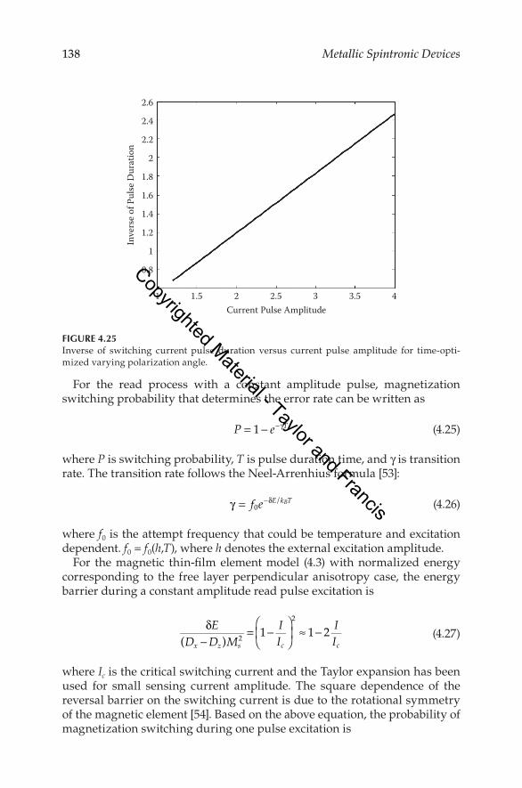
For the read process with a constant amplitude pulse, magnetization switching probability that determines the error rate can be written as
= − −γP e1 T (4.25)
where P is switching probability, T is pulse duration time, and γ is transition rate. The transition rate follows the Neel-Arrenhius formula [53]:
γ = −δf e E k T0
/ B (4.26)
where f0 is the attempt frequency that could be temperature and excitation dependent. f0 = f0(h,T), where h denotes the external excitation amplitude.
For the magnetic thin-film element model (4.3) with normalized energy corresponding to the free layer perpendicular anisotropy case, the energy barrier during a constant amplitude read pulse excitation is
δ−
= −
≈ −E
D D MII
II( )
1 1 2x z s c c
2
2
(4.27)
where Ic is the critical switching current and the Taylor expansion has been used for small sensing current amplitude. The square dependence of the reversal barrier on the switching current is due to the rotational symmetry of the magnetic element [54]. Based on the above equation, the probability of magnetization switching during one pulse excitation is
3.5 432.521.51
0.8
1.2
1.4
1.6
1.8
2.2
2.4
2.6
2
1
Current Pulse Amplitude
Inve
rse o
f Pul
se D
urat
ion
FIGURE 4.25Inverse of switching current pulse duration versus current pulse amplitude for time-opti-mized varying polarization angle.
Copyrighted Material - Taylor and Francis

139Memristive Effects and Magnetization Switching Optimizing
− −
− − −
Tf e1 expD D M
k TII
0
( ) 1 2x z sB c
2
(4.28)
For a given switching probability or error rate, the current pulse amplitude is proportional to the logarithmic of the pulse width. This scaling behavior is quite different from memristive scaling, where current pulse amplitude is proportional to the inverse of the pulse width.
However, it has been shown in [55–57] that the above scaling only holds for relatively long pulse durations. A “scale dilemma” results if we insist on using the above formula to describe short current pulse duration (~GHz) read disturbance. The reason is that detailed magnetization dynamics must be included to properly describe magnetization nonvolatility as read exci-tation frequency approaches the magnetization dynamical timescale. The above time-dependent energy barrier approach neglects the fast magnetiza-tion dynamic and is not sufficient to describe magnetization switching prob-ability for ultra-short pulse duration excitation.
Under the assumption that the spin torque excitation magnitude is well below the critical switching value, and based upon the stochastic Landau-Lifshitz-Gilbert equation with a spin torque term, the switching barrier reduction due to spin torque current excitation can be derived as [55, 56]
∫δ = χ ⋅β −−∞
∞
E t t t dtmin ( ) ( )t cc
(4.29)
where β(t) is the normalized spin torque proportional to polarized current magnitude, and χ(t) is the magnetization logarithmic susceptibility. The magnetization logarithmic susceptibility is defined as the ratio of reversal barrier reduction to external spin torque current excitation magnitude. tc in Equation (4.29) is the best time for the magnetization reversal to happen. Periodic external forcing lifts the time degeneracy of the escape path. It syn-chronizes optimal escape trajectories, one per period, to minimize the acti-vation energy of escape.
Magnetization logarithmic susceptibility χ(t) can be obtained from opti-mal reversal path zo(t), which is the minimization of functional action of the Landau-Lifshitz-Gilbert (LLG) equation with the spin torque term [55–57]. For a magnetic element with magnetization energy (4.3) and polarization pointing to the easy anisotropy direction,
{ } { }χ = − −
− α − − α −t D D e e( ) cos tan 1 cos tanx zD D t D D t1 ( ) 1 ( )
2x z x z (4.30)
Although the term switching barrier reduction has been used in describing the logarithmic susceptibility concept, the “barrier reduction” obtained through
Copyrighted Material - Taylor and Francis

140 Metallic Spintronic Devices
logarithmic susceptibility considers detailed magnetization dynamics. The LS switching barrier is not a static energy barrier based upon magnetization energy surface analysis. In the magnetization LS approach, through consid-ering detailed magnetization dynamics, the dynamics timescale at high fre-quency (~GHz) is retained for the long-time thermal magnetization reversal process. Thus, long-time thermal magnetization reversal dependence upon excitation frequency (up to GHz) is properly characterized.
As pulse duration decreases, the pulse width effect on switching prob-ability increases dramatically. This is because pulse duration directly affects thermal switching barrier reduction through magnetization logarithmic sus-ceptibility high-frequency components. Considering magnetization dynam-ics at high frequency, Equation (4.28) needs to be revised to
− −
− − −
Tf e1 expD D M
k Tr T I
I0
( ) 1 ( )x z sB c
2
(4.31)
where r(T) is the dynamic switching barrier reduction factor calculated from logarithmic susceptibility. Figure 4.26 shows the dynamic switching barrier reduction factor as a function of pulse duration. It becomes more and more significant as pulse duration decreases.
98765Time (second)
Reve
rsea
l Bar
rier R
educ
tion
Fact
or
432100.1
0.2
0.3
0.4
0.5
0.6
0.7
0.8
0.9
1
× 10–9
FIGURE 4.26Dynamic switching barrier reduction factor as a function of pulse duration. (From Z. Wang, et al., Appl. Phys. Lett. 103, 142419, 2013. With permission.)
Copyrighted Material - Taylor and Francis

141Memristive Effects and Magnetization Switching Optimizing
For a given switching probability, to the leading order, switching current amplitude and switching pulse duration can be related as
I I r T~ / ( )c (4.32)
Figure 4.27 shows the inverse of current pulse duration versus current pulse amplitude for constant error rate or switching probability. When dynamic effects are properly included, long-time thermal reversal shows obvious memristive effects.
Experiment measurements have been performed to verify the prediction of logarithmic susceptibility and the dynamic process in the spin torque ran-dom access memory read process [54, 58]. Figure 4.28 shows an example of measured current pulse duration versus current pulse amplitude [58]. The experiment confirms theoretical prediction of magnetization logarithmic susceptibility. Memristive behaviors are obvious in both experimental and theoretical models.
It should be pointed out that read operation memristive effects could have significant impacts on spin torque random access memory device operation and design. Due to the significant reduction of programming current for spin torque random access memory with improvement of magnetic tunnel-ing junction material and structure, the sense current margin for STT-MRAM design has been greatly tightened. Spintronic read memristive effects pro-vide dramatic reduction of read disturbance through pulse width control,
2.51.5Current Pulse Amplitude
Inve
rse o
f Pul
se D
urat
ion
(1/s
ec)
Solid: Dynamic logarithmicsusceptibility approachDash: Time varying energybarrier approach
10.5
Switching probabilit
y 10E–6
00
0.2
0.4
0.6
0.8
1.2
1.4
1.6
1.8
2
1
2 3
× 109
10E–8 10E–
10
10E–
12 10E–
14
FIGURE 4.27Inverse of read current pulse duration versus read pulse amplitude for different switching prob-abilities (or bit error rates). (From Z. Wang, et al., Appl. Phys. Lett. 103, 142419, 2013. With permission.)
Copyrighted Material - Taylor and Francis

142 Metallic Spintronic Devices
and thus open a new design possibility for SPRAM to achieve ultra-low write current and ultra-low read error at the same time.
4.6 Conclusion
Memristive effects are universal for spin torque spintronic devices at the timescale that explicitly involves the interactions between magnetization dynamics and electronic charge transport. This chapter explored spintronic memristive effects in emerging spin torque device operations. The universal features of spintronic memristive effects were illustrated in various write and read operating processes.
Although memristive effects could provide many exciting new application possibilities for spintronic devices, they also have quite strict constraints on
0 20 40 60
100
200
300
400
500
10–7
10–2
10–410–610–810–10
10–2
10–4
10–6
10–8
10–10
10–7
10–5
10–5
Pulse
Vol
tage
(mV)
Pulse Duration (ns)
(a)
10–310–3
100 200 300 400
0.0
0.2
0.4
0.6
Inve
rse o
f Pul
se D
urat
ion
(1/n
s)
Pulse Voltage (mV)
(b)
0 10 20 300.0
0.2
0.4
0.6
0.8
1.0
Nor
mal
ized
Pul
se A
mpl
itude
Pulse Duration (ns)
(c)
0.5 1.0 1.5 2.0
0.1
0.2
0.3
0.4
0.5
0.6In
vers
e of P
ulse
Dur
atio
n (1
/ns)
Normalized Pulse Amplitude
(d)
FIGURE 4.28Modeled and measured read current pulse duration versus read pulse amplitude for different read error rates (or switching probabilities). (From Z. Wang, et al., Appl. Phys. Lett. 103, 142419, 2013. With permission.)
Copyrighted Material - Taylor and Francis

143Memristive Effects and Magnetization Switching Optimizing
spintronic device write operations, such as writing speed and heat dissipa-tion. We studied spintronics device write optimization in light of its effects.
Memristive effects not only affect spintronic device write operation at the short-time dynamic magnetization reversal region, but also affect device read operations at the long-time thermal stability region. Experiment mea-surement and theoretical calculation reveal obvious memristive behaviors for short-pulse read operations. Dramatic reduction in read disturb through pulse width control provides a new design possibility for ultra-fast low-cur-rent STT-MRAM.
References
1. L. Berger, Phys. Rev. B 54, 9353, 1996. 2. J. C. Slonczewski, J. Magn. Magn. Mater. 159, L1, 1996. 3. W. F. Brown Jr., Phys. Rev. 130, 1677, 1963. I. N. Krivorotov, N. C. Emley, A. G. F.
Garcia, J. C. Sankey, S. I. Kiselev, D. C. Ralph, and R. A. Buhrman, Phys. Rev. Lett. 93, 166603, 2004. Z. Li and S. Zhang, Phys. Rev. B 69, 134416, 2004. D. M. Apalkov and P. B. Visscher, Phys. Rev. B 72, 180405(R), 2005. J. L. Garcia-Palacios and F. J. Lazaro, Phys. Rev B 58, 14937, 1998.
4. I. Theodonis, N. Kioussis, A. Kalitsov, M. Chshiev, and W. H. Butler, Phys. Rev. Lett. 97, 237205, 2006.
5. S. Salahuddin, D. Datta, P. Srivastava, and S. Datta, at IEEE Electronic Device Meeting, 2007.
6. J. Xiao and G. E. Bauer, Phys. Rev. B 77, 224419, 2008. 7. C. Heiliger and M. D. Stitles, Phys. Rev. Lett. 100, 186805, 2008. 8. A. Rebei, W. N. G. Hitchon, and G. J. Parker, Phys. Rev. B 72, 064408, 2005. 9. A. Manchon, N. Ryzhanova, N. Strelkov, A. Vedyayev, M. Chshiev, and B. Dieny,
J. Phys. Condens. Matter 20, 145208, 2008. 10. P. M. Haney, R. A. Duine, A. S. Nunezc, and A. H. MacDonald, J. Magn. Magn.
Mater. 320, 1300, 2008. 11. X. Wang, W. Zhu, and D. Dimitrov, Phys. Rev. B 79, 104408, 2009. 12. X. Wang, W. Zhu, and D. Dimitrov, Phys. Rev. B 78, 024417, 2008. 13. L. O. Chu, IEEE Trans. Circuit Theory 18, 507, 1971. 14. X. Wang, Y. Chen, H. Xi, and D. Dimitrov, IEEE Electron Device Lett. 30, 294, 2009. 15. G. Tatara and H. Kohno, Phys. Rev. Lett. 92, 086601, 2004. 16. R. A. Duine, A. S. Nunez, and A. H. MacDonald, Phys. Rev. Lett. 98, 056601, 2007. 17. D. B. Strukov, G. S. Snider, D. R. Stewart, and R. S. Williams, Nature 453, 80, 2008. 18. M. Di Ventra and Y. Pershin, Mater. Today 14, 584, 2011. 19. X. Wang and Y. Chen, in Design, Automation and Test Conference in Europe, 2010,
IEEE 10.1109/DATE.2010.5457118. 20. X. Lou, Z. Gao, D. V. Dimitrov, and M. X. Tang, Appl. Phys. Lett. 93, 242502, 2008. 21. E. Linn, R. Rosezin, C. Kugeler, and R. Waser, Nat. Mater. 9, 403, 2010. 22. W. Zhao, S. Chaudhuri, C. Accoto, J.-O. Klein, C. Chappert, and P. Mazoyer,
IEEE Trans. Nanotechnol. 11, 907, 2012.
Copyrighted Material - Taylor and Francis

144 Metallic Spintronic Devices
23. G. Snider, Appl. Phys. A 80, 1165, 2009. 24. D. Strukov and K. Likharev, Nanotechnology, 16, 888, 2005. 25. D. Strukov and K. Likharev, IEEE Trans. Nanotechnol. 6, 696, 2007. 26. S. Matsunaga, J. Hayakawa, S. Ikeda, K. Miura, H. Hasegawa, T. Endoh, H.
Ohno, and T. Hanyu, Appl. Phys. Express 1, 091301, 2008. 27. X. Lou, D. Dimitrov, and S. Xue, U.S. Patent 7855911, 2010. 28. S. Parkin, M. Hayashi, and L. Thomas, Science 320, 190, 2008 29. X. Wang, Y. Chen, Y. Gu, and H. Li, IEEE Device Lett. 31, 20, 2010. 30. G. Snider, Nanotechnology, 18, 1, 2007. 31. Y. Pershin and M. Ventra, Phys. Rev. E 84, 046703, 2011. 32. F. Merrikh-Bayat, S. Shouraki, and F. Merrikh-Bayat, in 2011 Eighth
International Conference on Fuzzy Systems and Knowledge Discovery (FSKD), 2011, 0.1109/FSKD.2011.6019541.
33. M. Klimo, O. Such, in Fourth International Conference on Future Computational Technologies and Applications, 2012, arXiv, 1110.2047.
34. T. Driscoll, J. Quinn, S. Klein, H. Kim, B. Kim, Y. Pershin, M. Ventra, and D. Basov, Appl. Phys. Lett., 97, 093502, 2010.
35. M. Itoh and L. Chua, Int. J. Bifurcation Chaos, 18, 3183, 2008. 36. M. Sharad, C. Augustine, G. Panagopoulos, and K. Roy, arXiv:1206.3227S. 37. S. Parkin, at Saudi International Nanotechnology Conference, 2010. 38. X. Wang, W. Zhu, S. Markus, and D. Dimitrov, IEEE Trans. Magn. 45, 2038, 2009. 39. X. Wang, Y. Chen, and T. Zhang, CMOS Processors and Memories, Springer,
Berlin, 2010. 40. M. Bardi and I. Capuzzo-Dolcetta, Optimal Control and Viscosity Solution of
Hamilton-Jacobi-Bellman Equations, Birkhauser, 2008. 41. R. Landauer, IBM J. Res. Dev. 5, 183, 1961. 42. K. Sekimoto, Prog. Theor. Phys. Suppl. 180, 17, 1998. 43. E. Aurell, C. Mejía-Monasterio, and P. Muratore-Ginanneschi, Phys. Rev. Lett.
106, 250601, 2011. 44. G. Monge, Histoire de l’Academie Royale des Sciences, Annee, 1781. Imprimerie
Royale, Paris, 666, 1784. L. Kantorovich, Acad. Sci. URSS, 37, 199, 1942. 45. J. Zhu, at MMM 2005 Conference, Paper CC-12. J. Zhu, X. Zhu, and Y. Tang, at
TMRC 2007 Conference, paper B6. J. Zhu, X. Zhu, and Y. Tang, IEEE. Trans. Magn. 44, 125, 2008.
46. Z. Z. Sun and X. R. Wang, Phys. Rev. B 73, 092416, 2006. 47. L. He and W. D. Doyle, IEEE Trans. Magn. 30, 4086. W. K. Hiebert, A.
Stankiewicz, and M. R. Freeman, Phys. Rev. Lett. 79, 1134, 1997. T. M. Crawford, T. J. Silva, C. W. Teplin, and C. T. Rogers, Appl. Phys. Lett. 74, 3386, 1999. Y. Acremann, C. H. Back, M. Buess, O. Portmann, A. Vaterlaus, D. Pescia, and H. Melchior, Science 290, 492, 2000. C. Thirion, W. Wernsdorfer, and D. Mailly, Nat. Mater. 2, 524, 2003. D. Xiao, M. Tsoi, and Q. Niu, J. Appl. Phys. 99, 013903, 2006.
48. H. W. Schumacher, C. Chappert, P. Crozat, R. C. Sousa, P. P. Freitas, J. Miltat, J. Fassbender, and B. Hillebrands, Phys. Rev. Lett. 90, 017201, 2003.
49. A. D. Kent, B. Zyilmaz, and E. del Barco, Appl. Phys. Lett. 84, 3897, 2004. 50. K. Rivkin and J. B. Kettersen, Appl. Phys. Lett. 89, 252507, 2006. 51. X. R. Wang and Z. Z. Sun, Phys. Rev. Lett. 98, 077201, 2007. 52. X. Wang, W. Zhu, Z. Gao, H. Xi, D. Dimitrov, Angular dependent spin torque,
J. Appl. Phys., 105, 07D103, 2009.
Copyrighted Material - Taylor and Francis

145Memristive Effects and Magnetization Switching Optimizing
53. L. Néel, Ann. Géophys. 5, 99, 1949. 54. X. Wang, W. Zhu, H. Xi, and D. Dimitrov, Appl. Phys. Lett. 93, 102508, 2008. 55. X. Wang, W. Zhu, H. Xi, Z. Gao, and D. Dimitrov, Appl. Phys. Lett. 93, 182506, 2008. 56. X. Wang and P. Ryan, J. Appl. Phys. 93, 182506, 2010. 57. X. Wang, SPIN World Sci. 2, 1240009, 2012. 58. Z. Wang, X. Wang, H. Gan, D. Jun, K. Satoh, T. Lin, Y. Zhou, J. Zhang, Y. Huai, Y.
Chang, and T. Wu, Appl. Phys. Lett. 103, 142419, 2013. 59. X. Wang and Y. Gu, J. Appl. Phys., 113, 126106, 2013.
Copyrighted Material - Taylor and Francis

Copyrighted Material - Taylor and Francis