Embed Size (px)
Citation preview
Fabrication and Characterization of
Ohmic Contacts
Project Thesis in Experimental Physics as a Part of the Master Curriculum in Nanoscience
Lukas Greuter*Quantum Coherence Lab, Zumbühl GroupDepartement of Physics, University of Basel
*Student of the Nanoscience-Curriculum, University of Basel, Switzerland
April - July 2009
CONTENTS 1
Abstract
To study electron transport phenomena at the interface in semiconductor heterostructures, providingelectrical contact is essential. In this project Au/Ge/Au/Ge/Pt ohmic contacts to a two-dimensionalelectron gas (2DEG) embedded in δ-doped GaAs/AlGaAs were fabricated and studied on two dierentwafers. Resistances were measured at room temperature and at 4K using a dipstick setup. The expecteddecrease of resistance was not observed for both wafers for low temperatures. The measured resistances ofthe ohmics showed a dependence on the annealing temperature during the fabrication process. Treatingthe heterostructure devices with an etching solvent prior to the deposition, was shown to increase theresistance of the contacts. Finally, surface studies with the Atomic Force Microscope (AFM) revealed adierence in roughness for surfaces treated with the etching solvent compared to non-treated surfaces.
Contents
1 Introduction 21.1 Two-dimensional electron gas in GaAs heterostructures . . . . . . . . . . . . . . . . . . . . . . 21.2 Theory of ohmic contacts . . . . . . . . . . . . . . . . . . . . . . . . . . . . . . . . . . . . . . 3
1.2.1 Metal-semiconductor interface . . . . . . . . . . . . . . . . . . . . . . . . . . . . . . . . 31.2.2 Composition of ohmic contacts . . . . . . . . . . . . . . . . . . . . . . . . . . . . . . . 51.2.3 Annealing mechanism . . . . . . . . . . . . . . . . . . . . . . . . . . . . . . . . . . . . 6
2 Fabrication of the ohmic contacts 72.1 Wafers used . . . . . . . . . . . . . . . . . . . . . . . . . . . . . . . . . . . . . . . . . . . . . . 72.2 Fabrication . . . . . . . . . . . . . . . . . . . . . . . . . . . . . . . . . . . . . . . . . . . . . . 82.3 Measurement . . . . . . . . . . . . . . . . . . . . . . . . . . . . . . . . . . . . . . . . . . . . . 9
3 Results 123.1 Dependence on the annealing temperature . . . . . . . . . . . . . . . . . . . . . . . . . . . . . 123.2 Eect of etching prior to evaporation . . . . . . . . . . . . . . . . . . . . . . . . . . . . . . . . 123.3 Conclusion . . . . . . . . . . . . . . . . . . . . . . . . . . . . . . . . . . . . . . . . . . . . . . 15
A Appendix - Fabrication protocol 17

1 INTRODUCTION 2
1 Introduction
Semiconductor materials gained huge attention in the 20th century since their special electronic behaviorallows the implementation of novel electronic components. Particularly the invention of transistors laid thefoundation for microelectronics, which is nowadays indispensable in many electronic equipments used ona daily basis. The high potential of semiconductors in industry was one of the reasons for the increasedresearch interest on that eld. Apart from the practical applications resulting from this research, many newinteresting physical phenomenas have been discovered in semiconductors.An interesting system, which arises in semiconductors is the formation of a two-dimensional electron gas(2DEG). A 2DEG is commonly found in metal-oxide-semiconductor eld-eect transistors (MOSFETs),where it arises at the semiconductor-oxide interface. This two-dimensional system allowed to study inter-esting physical phenomenons and lead to the description of the integer and fractional quantum hall eectin the beginning of the eighties [1], [2]. Few years later quantized conductance of quantum point contacts(QPC) dened in a 2DEG was observed using GaAs/AlGaAs heterostructures [3]. Furthermore the abilityto electrostatically dene quantum dots (often also referred to as articial atoms) enabled a lot of new pos-sibiltities to study fundamental physics. Especially the proposal to use electron spins conned in quantumdots to implement quantum bits(qubits) has gained a lot of attention in the last few years [4]. Such qubitswould allow the realization of a quantum computer that signicantly outperforms the computing ability ofclassical computers.Nowadays many experiments based on that proposal are carried out in quantum dots that are electrostaticallydened in a 2DEG embedded in GaAs/AlGaAs heterostructures [5]. For these kind of experiments providingelectrical contact to the 2DEG is essential. These contacts should be stable, easy to fabricate and ideallyobey Ohm's law. Such contacts are commonly realized by depositing a certain composition of metals onthe surface, which diuses into the semiconductor during a thermal annealing process. Although intensivelyresearch has been carried out in GaAs, there exist no absolute recipe for the fabrication of ohmic contactsin these structures since some steps in the fabrication are still not completely understood. However, thereexist only few systematic studies for the optimization of ohmic contacts. In this project the goal was tostudy Au/Ge/Au/Ge/Pt ohmic contacts to a 2DEG embedded in δ-dopped GaAs/AlGaAs heterostructures.Therefore Au/Ge/Au/Ge/Pt were successively evaporated on two dierent wafers with a mesa patterndened by optical lithography. The eect of using dierent temperatures during the annealing of the ohmiccontacts was studied by measuring the resistance at 4K. Furthermore, a new fabrication step was introduced:prior to the evaporation, the samples were pre-etched with a mixture of H2SO4 : H2O2 : H2O. Thisprocessing may lead to lower resistance values since it is thought that the etching generates a surfaceroughness, which could have a positive eect on the annealing mechanism. In the following, a short theoreticalbackground is provided before the fabrication protocol of ohmic contacts is described in detail. Finally,measured resistances are presented and compared among the dierent wafers and procedures used for thefabrication.
1.1 Two-dimensional electron gas in GaAs heterostructures
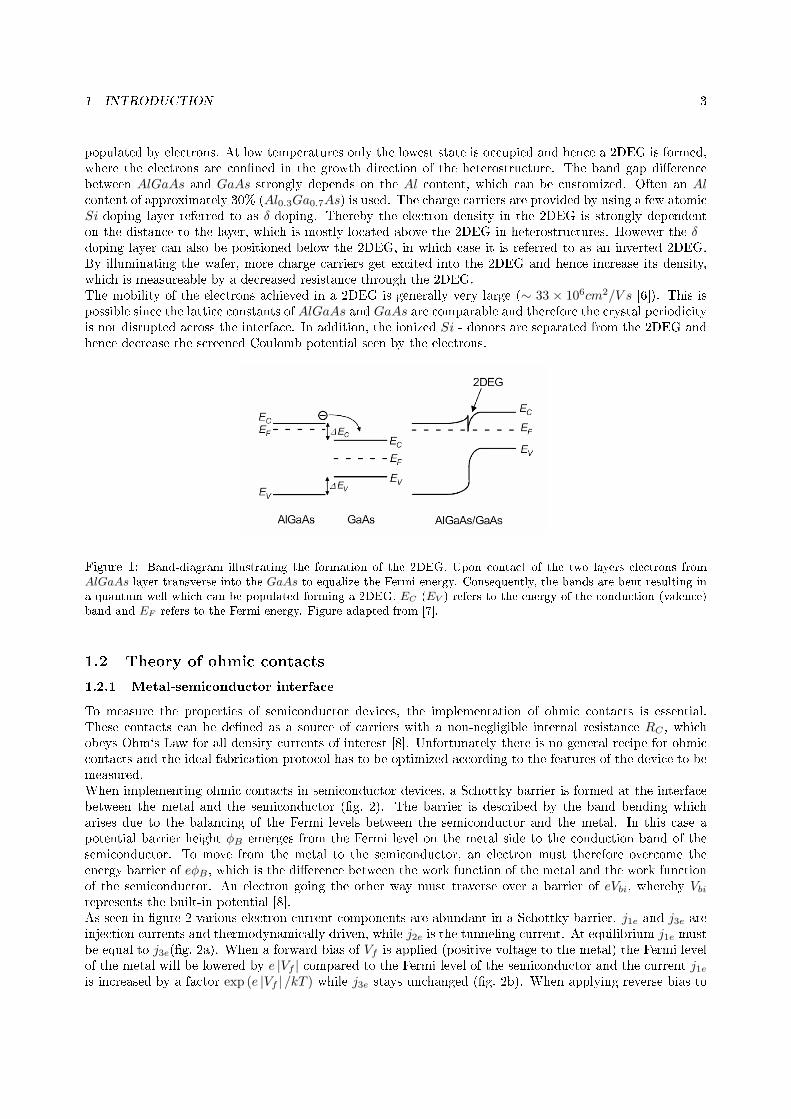
A 2DEG is formed at the interface between two semiconductor materials with dierent band gaps. This isthe case in GaAs/AlGaAs heterostructures, whereby the electrons from the material with the higher bandgap (AlGaAs) traverse into the material with the lower band gap (GaAs) in order to equalize the Fermienergy EF (g. 1). Consequently, the bands start to bend, which can be described when solving the Poissonequation [6]:
d2V
dz2= −qN
εε0(1)
Here V (z) describes the potential. The space charge density is given by ρ = qN , where N is the number ofdopants per m3. Since positive charge remains on the AlGaAs side the curvature of the conduction bandis positive (g. 1). Conversely, the curvature is negative at the GaAs side due to the presence of negativespace charge. The bending of the conduction band can be approximated by a triangular quantum well,in which discrete states are formed. If these states are lower in energy than the Fermi level EF they are
1 INTRODUCTION 3
populated by electrons. At low temperatures only the lowest state is occupied and hence a 2DEG is formed,where the electrons are conned in the growth direction of the heterostructure. The band gap dierencebetween AlGaAs and GaAs strongly depends on the Al content, which can be customized. Often an Alcontent of approximately 30% (Al0.3Ga0.7As) is used. The charge carriers are provided by using a few atomicSi-doping layer referred to as δ-doping. Thereby the electron density in the 2DEG is strongly dependenton the distance to the layer, which is mostly located above the 2DEG in heterostructures. However the δ -doping layer can also be positioned below the 2DEG, in which case it is referred to as an inverted 2DEG.By illuminating the wafer, more charge carriers get excited into the 2DEG and hence increase its density,which is measureable by a decreased resistance through the 2DEG.The mobility of the electrons achieved in a 2DEG is generally very large (∼ 33 × 106cm2/V s [6]). This ispossible since the lattice constants of AlGaAs and GaAs are comparable and therefore the crystal periodicityis not disrupted across the interface. In addition, the ionized Si - donors are separated from the 2DEG andhence decrease the screened Coulomb potential seen by the electrons.
Figure 1: Band-diagram illustrating the formation of the 2DEG. Upon contact of the two layers electrons fromAlGaAs layer transverse into the GaAs to equalize the Fermi energy. Consequently, the bands are bent resulting ina quantum well which can be populated forming a 2DEG. EC (EV ) refers to the energy of the conduction (valence)band and EF refers to the Fermi energy. Figure adapted from [7].
1.2 Theory of ohmic contacts
1.2.1 Metal-semiconductor interface
To measure the properties of semiconductor devices, the implementation of ohmic contacts is essential.These contacts can be dened as a source of carriers with a non-negligible internal resistance RC , whichobeys Ohm`s Law for all density currents of interest [8]. Unfortunately there is no general recipe for ohmiccontacts and the ideal fabrication protocol has to be optimized according to the features of the device to bemeasured.When implementing ohmic contacts in semiconductor devices, a Schottky barrier is formed at the interfacebetween the metal and the semiconductor (g. 2). The barrier is described by the band bending whicharises due to the balancing of the Fermi levels between the semiconductor and the metal. In this case apotential barrier height φB emerges from the Fermi level on the metal side to the conduction band of thesemiconductor. To move from the metal to the semiconductor, an electron must therefore overcome theenergy barrier of eφB , which is the dierence between the work function of the metal and the work functionof the semiconductor. An electron going the other way must traverse over a barrier of eVbi, whereby Vbirepresents the built-in potential [8].As seen in gure 2 various electron current components are abundant in a Schottky barrier. j1e and j3e areinjection currents and thermodynamically driven, while j2e is the tunneling current. At equilibrium j1e mustbe equal to j3e(g. 2a). When a forward bias of Vf is applied (positive voltage to the metal) the Fermi levelof the metal will be lowered by e |Vf | compared to the Fermi level of the semiconductor and the current j1eis increased by a factor exp (e |Vf | /kT ) while j3e stays unchanged (g. 2b). When applying reverse bias to

1 INTRODUCTION 4
Figure 2: Schottky barrier formed after contact between a metal and a semiconductor. Due to charge balancing, apotential barrier φB arises. When moving from the metal to the semiconductor the electron needs to overcome theenergy barrier eφB , while moving the other way an electron must traverse a barrier of eVbi. The current from themetal to the semiconductor(j3e) and vice versa (j1e) are equally at equilibrium because the net current vanishes (a).When applying forward bias (b) or reverse bias (c), the current j1e can be inuenced. In this situations the tunnelingcurrent j2e can be neglected since the barrier width is too big. Figure adapted from [8].

1 INTRODUCTION 5
the metal, its Fermi energy is raised by a factor of eVf (g. 2c) and consequently j1e is decreased by a factorof exp (e |Vf | /kT ). Again, j3e remains the same. This situation can be described by the diode equation [8]:
j = jrs
(eeV/kT − 1
)(2)
whereby j is the electron current from the metal to the semiconductor, dependent on the applied voltageV . jrs is the saturation current from the metal to the semiconductor, which is approximately constant fornegative V (reverse bias) until breakdown occurs. Since jrs depends on the barrier height φB equation 2can be written as:
j = Krse−eφB/kT
(eeV/kT − 1
)(3)
where Krs is a constant. Apart from very low voltages (V kT/e), the situation described by equation 3does not represent a contact that obeys Ohm`s law. Furthermore the current also depends on the factorexp (−eφB/kT ). Since eφB kT for GaAs already at normal temperatures, the current j in equation 3 ismainly limited by the barrier height φB and clearly not ohmic.To achieve a high current density φB has to be decreased by a proper choice of the metal. In GaAs this isnot possible due to the large surface state density. Therefore to achieve ohmic behavior the width of theSchottky barrier wd must be decreased so that the tunneling current plays a central role. The tunnelingprobability can be estimated by the Wentzel-Kramers-Brillouin (WKB) approximation [6]:
T (wd) = exp
[−2∫ 0
wd
2m∗
h2 V (z)1/2
dz
](4)
Here V (z) describes the shape of the potential and V (wd) = 0. V (z) is obtained when solving the Poissonequation and with using the depletion depth wd the integral can be calculated and the tunnel probabilitybecomes:
T = expe(V − Vbi)
E0(5)
where ∆V = V −Vbi represents the dierence between the external applied voltage V and the bias indepen-dent barrier height Vbi. E0 is the energy, dependent on the doping density N :
E0 =h
2
(e2N
εε0m∗
)1/2
(6)
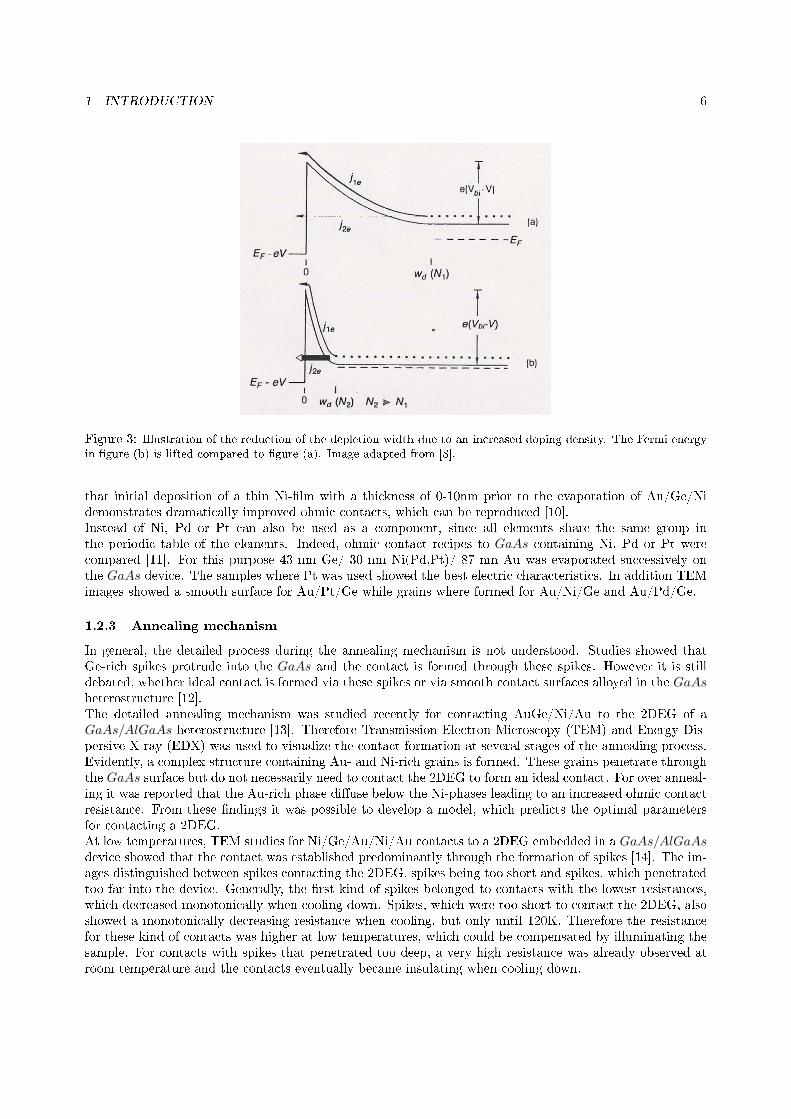
Evidently, increasing the doping density decreases the depletion width. Consequently, the tunnel probabilityincreases according to the equations 5 and 6. The situation is described in gure 3. By increasing the dopingdensity, the Fermi energy is lifted closer to the conduction band and the depletion depth is decreased,resulting in a higher tunnel probability. For very high doping densities the barrier gets very narrow and thecontact between the metal and the semiconductor can be regarded as an ohmic contact.
1.2.2 Composition of ohmic contacts
Although the 2DEG in GaAs-heterostructures is widely used to study dierent mesoscopic behaviors, thereexists no general metallic composition of the ohmic contacts up to now. However the Au/Ge eutectic, whichmelts at around 360C is considered to be a permanent feature among the dierent ohmic contact recipes.Au is thereby assumed to act as the carrier, while Ge is thought to diuse into the semiconductor to providethe doping, which decreases the tunnel barrier. The used weight ratio of the eutectic is typically 88% : 12%.Additional to the Au/Ge eutectic, Ni was often used as a compound of the contact metal alloys [9],[10].Thereby the ohmic contacts yield low resistances when the Ni-layer was evaporated as the last layer. Theoptimal Ni-layer thickness was determined to be approximately one quarter of the total Au/Ge layer thick-ness. Furthermore, it was shown that evaporation of 107.2 nm of Au, 52.8nm of Ge, followed by 40 nm of Nigives very reasonable contacts, which were later used for various 2DEG devices [9]. Another study showed
1 INTRODUCTION 6
Figure 3: Illustration of the reduction of the depletion width due to an increased doping density. The Fermi energyin gure (b) is lifted compared to gure (a). Image adapted from [8].
that initial deposition of a thin Ni-lm with a thickness of 0-10nm prior to the evaporation of Au/Ge/Nidemonstrates dramatically improved ohmic contacts, which can be reproduced [10].Instead of Ni, Pd or Pt can also be used as a component, since all elements share the same group inthe periodic table of the elements. Indeed, ohmic contact recipes to GaAs containing Ni, Pd or Pt werecompared [11]. For this purpose 43 nm Ge/ 30 nm Ni(Pd,Pt)/ 87 nm Au was evaporated successively onthe GaAs device. The samples where Pt was used showed the best electric characteristics. In addition TEMimages showed a smooth surface for Au/Pt/Ge while grains where formed for Au/Ni/Ge and Au/Pd/Ge.
1.2.3 Annealing mechanism
In general, the detailed process during the annealing mechanism is not understood. Studies showed thatGe-rich spikes protrude into the GaAs and the contact is formed through these spikes. However it is stilldebated, whether ideal contact is formed via these spikes or via smooth contact surfaces alloyed in the GaAsheterostructure [12].The detailed annealing mechanism was studied recently for contacting AuGe/Ni/Au to the 2DEG of aGaAs/AlGaAs heterostructure [13]. Therefore Transmission Electron Microscopy (TEM) and Energy Dis-persive X-ray (EDX) was used to visualize the contact formation at several stages of the annealing process.Evidently, a complex structure containing Au- and Ni-rich grains is formed. These grains penetrate throughthe GaAs surface but do not necessarily need to contact the 2DEG to form an ideal contact. For over anneal-ing it was reported that the Au-rich phase diuse below the Ni-phases leading to an increased ohmic contactresistance. From these ndings it was possible to develop a model, which predicts the optimal parametersfor contacting a 2DEG.At low temperatures, TEM studies for Ni/Ge/Au/Ni/Au contacts to a 2DEG embedded in a GaAs/AlGaAsdevice showed that the contact was established predominantly through the formation of spikes [14]. The im-ages distinguished between spikes contacting the 2DEG, spikes being too short and spikes, which penetratedtoo far into the device. Generally, the rst kind of spikes belonged to contacts with the lowest resistances,which decreased monotonically when cooling down. Spikes, which were too short to contact the 2DEG, alsoshowed a monotonically decreasing resistance when cooling, but only until 120K. Therefore the resistancefor these kind of contacts was higher at low temperatures, which could be compensated by illuminating thesample. For contacts with spikes that penetrated too deep, a very high resistance was already observed atroom temperature and the contacts eventually became insulating when cooling down.

2 FABRICATION OF THE OHMIC CONTACTS 7
2 Fabrication of the ohmic contacts
2.1 Wafers used
Two dierent GaAs/AlGaAs heterostructures, referred to as Pinto 15 and 16, were used for studying theohmic-contact fabrication recipes. Both wafers were grown by Antonio Badolato in the Wegscheider groupat the University of Regensburg. Figure 4 shows the growth prole for the two wafers, which were grown bymolecular beam epitaxy (MBE). In both structures two 2DEGs are formed: an inverted 2DEG at the interfacebetween the AlGaAs spacer layer and GaAs tunnel barrier as well as a 2DEG at the AlGaAs/GaAs-buerlayer interface. The red layers indicate the location of self assembled InAs quantum dots. In this projecthigh density (HD) wafers containing the quantum dots and low density (LD) wafers without the quantumdots were used. The distance from dots to the inverted 2DEG is referred to as the tunnel barrier and denesthe tunneling rate from the 2DEG into the self-assembled quantum dots. Both structures reveal a dierentthickness of the spacing layer, which is the distance of the Si− δ-doping to the 2DEG. The thickness of thelayer strongly inuences the density of the 2DEG. By decreasing the spacer layer thickness the tunneling rateincreases which results in a higher density of the 2DEG. However, the ionized Si donors are a relevant sourceof scattering and therefore the mobility of the 2DEG is strongly aected when decreasing the thickness ofthe spacer layer. A relatively thick AlGaAs blocking barrier prevents charge transfer between the quantumwell and the surface of the layer, which is important when using top gates. Furthermore, the thickness of theblocking barrier has as well an inuence on the density of the 2DEG. The top GaAs layer has the functionof a capping layer and protects the underlying AlGaAs layer from oxidation. Compared to Pinto 15, Pinto16 contains an additional AlGaAs sacricial layer which can be etched when requested.Figure 5 shows the conduction band of Pinto 16 obtained when solving the Poisson and the Schrödingerequation for specied layer thicknesses and material properties (GaAs or AlGaAs and Al content) [15].According to the growth prole a 2DEG forms 152 nm and 282 nm below the surface due to the formationof a quantum well at the GaAs/AlGaAs-interface. The δ-doping layer causes a charge dipole between thesurface and the doping layer as well as between the doping layer and the heterointerface. Both dipoles resultin an electric eld which gives constant slopes of the conduction band (g. 5).
Figure 4: Growth prole of Pinto 15 (left) and 16 (right), grown by molecular beam epitaxy (MBE). The maindierence is the location of the δ-doping layer with respect to the 2DEG. In addition a sacricial AlGAs layer isimplemented in Pinto 16.

2 FABRICATION OF THE OHMIC CONTACTS 8
0 50 100 150 200 250 300 350 400 450 500 550
-1
-0.8
-0.6
-0.4
-0.2
0
0.2
Distance from surface (nm)
ConductionBandEnergy(eV)
Subband Levels
Fermi Energy
Conduction Band
InAs Energy Level
Figure 5: Conduction band structure of Pinto 16. A quantum well forms when the conduction band is below inenergy than the fermi energy Graph provided by F. Dettwiler.
2.2 Fabrication
For all wafers the following main steps were pursued in the fabrication (For a detailed fabrication protocolsee appendix):
1. Optical lithography of the mesa pattern
2. Etching of the mesa pattern
3. Optical lithography of the ohmic contacts
4. Evaporation of the ohmic contacts
5. Annealing
6. Wire-bonding
To dene the mesa structures by optical lithography, negative photoresist (ma-N 415) was spin-coated onthe pre-cleaned samples. The photoresist is hardened and therefore insoluble when exposed to light, whilethe unexposed regions dissolve during the development. A mask precisely denes which areas are unexposedduring the lithography. After illuminating and developing, the remaining resist represents the mesa patternand protects the underlying area from being etched (g. 6a). Thus the etched mesa pattern was initiallydened by the layout of the mask.For the etching a mixture of H2SO4 : H2O2 : H2O with a ratio of 2:16:480 was used. Thereby the hydrogenperoxide acts as the oxidizing agent while the sulfuric acid dissolves the resulting oxide. The etching rate wasdetermined to be ∼140 nm/min, which is in good agreement with literature values [16]. Pinto 15(16) wasetched 280(300) nm until the GaAs buer layer. This is necessary, since etching until the AlGaAs layer only,may cause lift-o problems due to the oxidation of AlGaAs. After the mesa etch and removing of the photoresist with NMP, the samples were spin coated with negative photo resist again to dene the ohmic contacts.

2 FABRICATION OF THE OHMIC CONTACTS 9
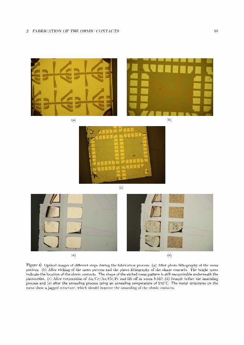
In gure 6b the wafer is shown after the photo lithography of the ohmic contacts. The bright spots indicatethe location of ohmic contacts, while the rest is covered with photoresist. The samples were then treatedwith oxygen plasma in order to clean impurities on the resist. Before evaporation two dierent procedureswere distinguished. For the one procedure, the samples were dipped into HCl prior to the evaporation toremove remaining oxides from the oxygen plasma. For the other procedure the samples were dipped into amixture of H2SO4 : H2O2 : H2O with the ratio of 1:8:1000 corresponding to a etching rate of ∼40 nm/min.The goal of this pre-etching was to increase the roughness at the ohmic contact spots, which may has aneect on the adhesion of the metals as well as on the diusion during the annealing cycle.During the evaporation process Au/Ge/Au/Ge/Pt with thicknesses 120 nm/60 nm/120 nm/60 nm/85 nmwere deposited successively on the surface starting with Au. Hereby the Au/Ge builds the eutectic mixtureand Pt prevents the `balling up' from Au/Ge. After the evaporation, the lift-o was done by putting thesamples into warm NMP. NMP dissolves hardened negative photo resist and therefore the deposited metalis removed except for the ohmic contact spots, which were not covered by the photoresist (g. 6c). In theannealing cycle the samples were rst heated to 370C for 2 min to melt the eutectic mixture. Subsequently,the samples were annealed at 420C, 450C, 480C or 510C for 1 min (g. 6e). Note that the ohmics onlyform contact with the 2DEG only on spots with underlying mesa pattern. In the other regions it was etchedinto the GaAs buer layer and hence no 2DEG is present there. These contacts are used to implement thetop gates, which were not required for this project. The last step was to wire bond the ohmic contacts usingAl wire.
A dierent lift-o behavior was observed for Pinto 16 LD which was dipped into HCl and Pinto 16 LDwhich was pre-etched prior to the evaporation. Generally sticking problems occurred more often to thesample treated with H2SO4 : H2O2 : H2O (g. 7). Such problems can occur, when the photoresist wasunderdeveloped. This is not the case here since both structures were processed following the exact sameprotocol. Moreover, the adhesion problems could be due to the possible oxidation of the AlGaAs for Pinto16 LD treated with H2SO4 : H2O2 : H2O. This would imply that at least the whole capping layer of 12nm thickness was etched away. At rst sight this seems rather unlikely since the etching time was chosen inaccordance with the determined etching rate so that only 5 nm are etched. However it is possible that theetching rate is not uniform in time and that in fact more than 5 nm were etched. In gure 7b the ohmicspots at the mesa are indeed brightened, which could indicate a too high etching.
2.3 Measurement
The ohmic contact resistances were measured at room temperature and at 4K using a helium dewar dipsticksetup. In addition the samples were also illuminated to increase the density of the 2DEG. Two dierentmeasurement techniques were used: the battery measurement and the lock-in technique. When using thebattery measurement a known voltage of 10 mV was applied to the sample via the contact to be measured.By measuring the current through the sample the resistance could be determined using Ohm's law. Themeasured resistance consists not only of the resistance of the ohmic contact but also of the resistance of thebattery as well as of the resistance of the dipstick wiring. Since the remaining ohmics were put on groundcurrent also owed through these contacts and the total measured resistance is given by:
Rmeas = Rwire +Rbatt +Rohm +Rrest (7)
The resistance of the wiresRwire and the batteryRbatt were determined to be 220 Ω and 9.107 kΩ respectively.The remaining ohmic contacts were all connected to the ground, which means that they are connected inparallel. Therefore, the resistance Rrest can be describes as:
1Rrest
=1R1
+1R2
+1R3
+ ... (8)
where R1, R2, R3 and so forth represent ohmic contacts which are not measured. It is obvious that Rrestdecreases the more contacts are connected in parallel. Therefore, the Rrest is neglected and we determinethe resistance of one specic ohmic using:
2 FABRICATION OF THE OHMIC CONTACTS 10
(a) (b)
(c)
(d) (e)
Figure 6: Optical images of dierent steps during the fabrication process. (a) After photo lithography of the mesapattern. (b) After etching of the mesa pattern and the photo lithography of the ohmic contacts. The bright spotsindicate the location of the ohmic contacts. The shape of the etched mesa pattern is still recognizable underneath thephotoresist. (c) After evaporation of Au/Ge/Au/Ge/Pt and lift o in warm NMP. (d) Sample before the annealingprocess and (e) after the annealing process using an annealing temperature of 510C. The metal structures on themesa show a jagged structure, which should improve the annealing of the ohmic contacts.

2 FABRICATION OF THE OHMIC CONTACTS 11
(a) (b)
Figure 7: Comparison of the lift o for Pinto 16 LD dipped in HCl (a) and Pinto 16 LD pre-etched (b). Obviously,lift-o problems occurred for the pre-etched sample, which could be due to the oxidation of AlGaAs. The brightenedspots in (b) indeed indicate that more than 5 nm was etched.
Rohm = Rmeas −Rwire −Rbatt (9)
When using the lock-in technique, an AC - current of 10.17nA was applied to the sample and the resultingvoltage was measured. The lock-in acts as an extremely narrow band-pass lter allowing to lter noisecomponents at unwanted frequencies resulting in a more accurate measurement. To calculate the specicohmic contact resistance only the resistance of the wire Rwire was subtracted from the measured resistanceRmeas since no battery was present. However, the measurements did not reveal any signicant dierencesbetween the battery and the lock-in measurements.

3 RESULTS 12
3 Results
3.1 Dependence on the annealing temperature
In gure 8a the average ohmic contact resistance of Pinto 15 HD is plotted as a function of annealingtemperature measured at room temperature (RT) and at 4K. The resistance seems to be optimal for anannealing temperature of 450C and increases when further increasing the annealing temperature. A similarbehavior was also reported for Au/Pt/Ge ohmics, which also showed optimal resistances for samples annealedat 450C [11]. Furthermore, the resistances measured at room temperature were much lower than formeasurements performed at 4K. Such an eect is clearly not expected since low temperatures should minimizescattering eects and hence decrease the resistance. However, it is possible that the ohmic did not makecontact to the 2DEG during the annealing mechanism resulting in a increased resistance for low temperaturesas reported earlier [14].Figure 8b shows the average ohmic contacts resistance for Pinto 16 LD at 4K. Compared to Pinto 15 HDthe resistances are much lower and seem to further decrease by increasing annealing temperature. The lowerdata points reveal the measured resistances at 4K after illuminating the sample for 1 min. The resistance isobviously dramatically decreased due to the additional charge carriers, which were excited into the 2DEG.Generally the resistances of Pinto 15 HD were much higher than the resistances measured for Pinto 16 LD at4K, while at room temperature the resistances were comparable. For example at an annealing temperatureof 450C the resistances of Pinto 15 HD are around 30 kΩ while for the non-illuminated Pinto 16 LD samplesthe resistance was determined to be around 500 Ω. This dierence maybe a consequence of the relativelysmall spacer layer, which strongly aects the mobility of the 2DEG in Pinto 15HD (g. 4). However, asmentioned above, a poor contact to the 2DEG could also be the reason of this observation.
(a) (b)
Figure 8: Dependence of the ohmic contact resistances on the annealing temperature. (a) Pinto 15 HD measured atroom temperature (RT) and at 4K. (b) Pinto 16 LD measured at 4K before and after illumination by a LED.
3.2 Eect of etching prior to evaporation
The eect of etching the ohmic contact spots prior to the evaporation was studied using Pinto 16 LD annealedat 480C and 510. Thereby Pinto 16 LD rinsed in HCl before the evaporation was compared to Pinto 16LD etched prior to the evaporation using a mixture of H2SO4 : H2O2 : H2O. Table 1 summarizes the resultsobtained from this comparison.Evidently, the ohmic resistance of the pre-etched samples is not lower compared to the ohmics rinsed inHCl. This implies that the pre-etching had no inuence during the annealing mechanism. In contrary, theresistances are even as twice as high for measurements on non-illuminated as well as illuminated samples.The reason for this observation is not quite clear. A possible explanation could be that the AlGaAs layer
3 RESULTS 13
SampleAnnealing Resistance 4K Resistance 4K
temperature [C] before illuminating [kΩ] after illuminating [kΩ]Pinto 16 LD 480 ∼1.0 ∼0.3(rinsed in HCl) 510 ∼0.5 ∼0.2Pinto 16 LD 480 ∼2.0 ∼0.6(pre-etched) 510 ∼1.9 ∼0.4
Table 1: Comparison between the samples etched before the evaporation and the samples treated with HCl.
was oxidized during the process. However, the GaAs capping layer should not be etched away completelyduring the pre-etching. Further it is rather unlikely that the etching of the surface inuenced the actualelectron mobility of the 2DEG since only a few nanometers were etched.
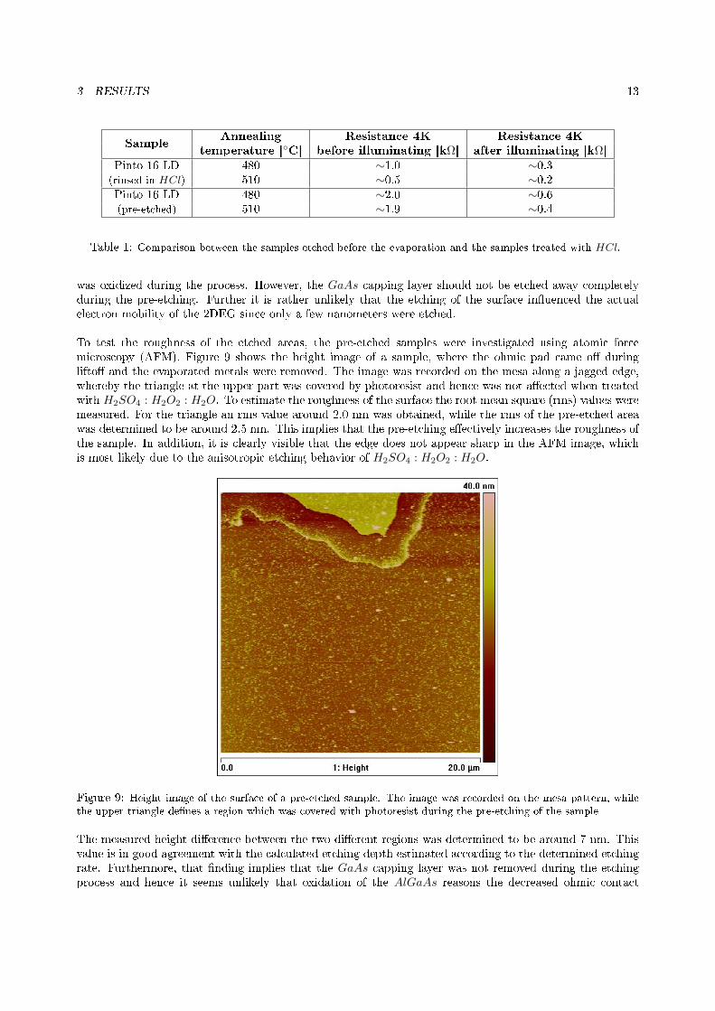
To test the roughness of the etched areas, the pre-etched samples were investigated using atomic forcemicroscopy (AFM). Figure 9 shows the height image of a sample, where the ohmic pad came o duringlifto and the evaporated metals were removed. The image was recorded on the mesa along a jagged edge,whereby the triangle at the upper part was covered by photoresist and hence was not aected when treatedwith H2SO4 : H2O2 : H2O. To estimate the roughness of the surface the root mean square (rms) values weremeasured. For the triangle an rms value around 2.0 nm was obtained, while the rms of the pre-etched areawas determined to be around 2.5 nm. This implies that the pre-etching eectively increases the roughness ofthe sample. In addition, it is clearly visible that the edge does not appear sharp in the AFM image, whichis most likely due to the anisotropic etching behavior of H2SO4 : H2O2 : H2O.
Figure 9: Height image of the surface of a pre-etched sample. The image was recorded on the mesa pattern, whilethe upper triangle denes a region which was covered with photoresist during the pre-etching of the sample
The measured height dierence between the two dierent regions was determined to be around 7 nm. Thisvalue is in good agreement with the calculated etching depth estimated according to the determined etchingrate. Furthermore, that nding implies that the GaAs capping layer was not removed during the etchingprocess and hence it seems unlikely that oxidation of the AlGaAs reasons the decreased ohmic contact

3 RESULTS 14
resistance of the pre-etched samples.Figure 10 shows a zoom in on the etched and non etched area. The rms values for these images weredetermined to be around 0.21 nm for the non-etched (left side of gure 10) and 0.36 nm for the etched area(right side of gure 10). Note that these rms values dier from the values obtained from gure 9 by a factorof ten due to the higher resolution obtained in gure 10.
Figure 10: AFM measurements of the areas, which were pre-etched surface (left) and the non-etched areas (right).The photograph was taken before the sample was treated with H2SO4 : H2O2 : H2O and illustrates which positionsof the mesa were examined with the AFM.

3 RESULTS 15
3.3 Conclusion
The ohmic contact recipe using Au/Ge/Au/Ge/Pt was shown to be successfully implemented. The measure-ments showed quite some dierence between Pinto 15 and Pinto 16 at 4K: While measurements for Pinto15 revealed resistances between 54 and 27 kΩ, resistances lower than 1.0 kΩ were obtained for Pinto 16. Incontrary, room temperature measurements showed resistances around 20 kΩ for both wafers. Furthermorethe annealing temperature for Pinto 15 wafers seem to have an optimum around 450C, while for Pinto 16the resistances seem to decrease further with increasing the annealing temperature. The dierence in resis-tance between Pinto 15 and 16 is not clearly understood. A possible explanation could be that the δ-dopinglayer is located closer to the 2DEG in Pinto 15. This would decrease the mobility of the electrons in the2DEG, since the Si-donors are a relevant source of scattering. However, locating the δ-doping layer closerto the 2DEG could also increase its density, which would be observable in a lowered resistance. However tounderstand the exact behavior of these two counteracting eects, a systematical study using several dierentwafers with a dierent spacer layer thickness would be necessary.Another possible explanation of the dierence in resistances could be that the ohmics on the Pinto 15 wafersdo not form proper contacts to the 2DEG during the annealing process. This could be the reason, whythe resistance is increased when cooling down: charge carriers which contributed to the current at roomtemperature are now frozen in, while the reduction of scattering eects in the 2DEG has little eect due tothe lack of proper ohmic contact. However, this reasoning assumes that the annealing mechanism for Pinto15 diers from the annealing mechanism in Pinto 16. This is rather unlikely, because the growth prole fromthe surface to the 2DEG is identical for both wafers (assuming we measure the inverted 2DEG). Similarly aconsequence of overannealing for the Pinto 15 wafers can be excluded for the same reason.It is further unclear, whether the presence of self assembled quantum dots has an inuence on the resistancemeasurements presented above. Unfortunately it was not possible to directly compare wafers with dots toidentical wafers without dots. Such a comparison is insofar interesting for potential future experiments usingelectrons trapped in the self-assmbled InAs quantum dots.
Pre-etching the samples prior to the evaporation did not have the anticipated eect. In contrary it wasreported that the resistance even increase when treating the sample with H2SO4 : H2O2 : H2O. The reasonfor this is unclear since oxidation of the AlGaAs layer should not occur and the etching should also notaect the electron mobility in the 2DEG. Furthermore, more lift-o problems were experienced when thesamples where pre-etched. However, the AFM images conrm rougher surfaces for pre-etched samples butit seems that this does not inuence the annealing mechanism.
The achieved resistances below 1.0 kΩ in Pinto 16 wafers is already quite low. However, it is desirableto have minimized ohmic contact resistances. Generally, the composition of the recipe can be alternatedto improve the ohmic contacts. A possibility would be to study the eect of dierent annealing times onthe ohmic contact resistances. Moreover, since the resistance of Pinto 16 wafers seem to further decreasewith increasing annealing temperature, an opportunity would also be to use higher annealing temperatures.Alternatively, the composition of the metals used could also be varied by introducing a wetting layer forexample, which could increase the adhesion of the metals. However, since the annealing mechanism is mainlyremains unclear it is rather dicult to state concrete proposals in order to improve the ohmic contacts.
Acknowledgement
Primarily, I would like to thank Florian Dettwiler, who explained me all the machines used for fabricationand for being always helpful and patient when I had problems. I would also like to acknowledge Prof.Dominik Zumbühl for giving valuable inputs on the project and for the possibility to accomplish this projectwithin his group. Further thanks go to Antonio Badolato from the Wegscheider group for providing us withthe heterostructures. Finally, I would like to thank all the group members of the Zumbühl group for alwaysbeing willing to answer my questions.

REFERENCES 16
References
[1] von Klitzing K., Dorda G., Pepper M. New Method for High-Accuracy Determination of the Fine Struc-ture Constant Based on Quantized Hall Resistance. Physical Review Letters 45 (6), 1980
[2] Tsui D.C., Stormer H.L., Gossard A. C. Two-Dimensional Magnetotransport in the Extreme QuantumLimit. Physical Review Letters 48 (22), 1982
[3] van Wees B.J., van Houten H., Beenakker C.W.J., Williamson J.G., Kouwenhoven L.P., van der MarelD., Foxon C.T. Quantized Conductance of Point Contacts in a Two-Dimensional Electron Gas. PhysicalReview Letters 60 (9), 1988
[4] Loss D., DiVincenzo D. P. Quantum Computing with quantum dots. Physical Review A 57 (1), 1998
[5] For a review see for example: Hanson R., Kouwenhoven L.P., Petta J.R., Tarucha S., Vandersypen L.M. K., Spins in few-electron quantum dots. Reviews of Modern Physics 79, 2007
[6] Zumbühl D. Introduction to Mesoscopic Physics and Quantum dots Lecture at the Institute of Physics,University of Basel HS 2008
[7] Oberholzer S. Nano-Elektronik. Lecture at the Institute of Physics, University of Basel HS 2007
[8] Look D.C. Electrical Characterization of GaAs Materials and Devices. Design and Measurement in Elec-tronic Engineering (1988)
[9] Göktas O., Weber J., Weis J., von Klitzing K. Alloyed ohmic contacts to two-dimensional electron systemin AlGaAs/GaAs heterostructures down to submicron length scale. Physica E (2008) 1579-1581
[10] Valeille A., Muraki K., Hirayama Y. Highly reproducible fabrication of back-gated GaAs/AlGaAs het-erostructures using AuGeNi ohmic contacts with initial Ni layer. Applied Physics Letters, 92, 152106(2008)
[11] Lin C., Lee C.P., Comparison of Au/Ni/Ge, Au/Pd/Ge and Au/Pt/Ge Ohmic contacts to n-type GaAs.J.Appl. Phys. 67(1), 1990
[12] Fleischer M. Transporteigenschaften von Quantenpunktkontakten und Quantenpunkten. DissertationEberhard Karls Universität zu Tübingen (2006)
[13] Koop E.J., Iqbal M.J., Limbach F., Boute M., van Wees B.J., Reuter D., Wieck A.D., Kooi B.J., vander Waal C.H. The annealing mechanism of AuGe/Ni/Au ohmic contacts to a two-dimensional electrongas in GaAs/AlxGa1−xAs heterostructures. arXiv:0809.0928 (2008)
[14] Taylor R.P., Coleridge P.T., Davies M., Feng Y., McCarey J.P., Marshall P.A. Physical and electricalinvestigation of ohmic contacts to AlGaAs/GaAs heterostructures. J. Appl. Phys. 76 (12), 1994
[15] Dettwiler F. Fabrication of Lateral Self-Assembled Hybrid Nanostructures. Master's Thesis 2008
[16] Williams R. Modern GaAs Processing Methods. Artech House 1994
A APPENDIX - FABRICATION PROTOCOL 17
A Appendix - Fabrication protocol
Optical lithography of the mesa pattern
• cleaving GaAs/AlGaAs with diamond scribe
• clean samples: 3 solvent clean: 5 min. TCE, 5 min. Acetone, 5 min. Methanol each in ultrasound
• blow o samples with N2
• pre-bake samples on hot plate: 120C for 5 min., let cool for 2 min.
• spin photoresist (ma-N415), 6000 rpm, 40s, ramp time: 6s
• bake on hot plate 93C, 90s
• expose on mask aligner: for 7.0s, use hard contact time 2.0s, pressure: 1.4 bar
• develop for 60s in developer (ma-D 332S)
Etching of the mesa pattern
• measure thickness of the resist with α - stepper
• prepare etching solvent H2SO4 : H2O2 : H2O mixture 2:16:480
• determine etching rate by etching a test sample for 1 min. and measure depth with α - stepper
• etch 280 nm (Pinto 15) 300 nm (Pinto 16)
• remove resist: put samples into warm NMP (45-50C)
• verify etching depth using α - stepper
• blow o with N2 gun
Optical lithography of the ohmic contacts
• 3-solvent clean and prebake at 120C for 5 min
• spin photoresist (ma-N415), 6000 rpm, 40s ramp time; 6s
• bake at 93C for 90s
• align sample with ohmic pattern on the mask
• expose on mask aligner: for 7.0s, use hard contact time 2.0s, pressure: 1.4 bar
• develop 60s in developer (ma-D 332S)
• check with optical microscope develop longer if necessary
A APPENDIX - FABRICATION PROTOCOL 18
Evaporation of the ohmic contacts
• prepare etching solvent H2SO4 : H2O2 : H2O 1:8:1000 and calibrate etching rate
• calibrate oxygen plasma using a test sample covered with photoresist illustrating a mesa pattern
• etch '40 nm with oxygen plasma
• Choose between following steps:
dip sample 5s in HCl rinse in DI H2O
etch 5 nm in H2SO4 : H2O2 : H2O 1:8:1000 and rinse in DI H2O
• load sample into evaporator, pumping, cooling down to 0C
• evaporate successively:
120 nm Au
60 nm Ge
120 nm Au
60 nm Ge
85 nm Pt
• lift o in warm NMP for 30 min. clean with syringes
Annealing & wire bonding
• anneal samples:
2min. 370C
1 min. 420C, 450C, 480C or 510C
• cleave samples if requested
• wire bonding using Al wire


![Performance Comparison of Graphene Nanoribbon … the channel to metals with Schottky contacts [8, 14], therefore obtaining a Schottky barrier FET (SBFET). In addition, ohmic contacts](https://img.dokumen.tips/doc/110x75/5b26cfe77f8b9afc678b54f4/performance-comparison-of-graphene-nanoribbon-the-channel-to-metals-with-schottky.jpg)