Embed Size (px)
Citation preview

TD-R124 689 STUDY OF OHMIC CONTACTS ON SI(28) - IMPLANTED GAAS(U) /AIR FORCE INST 0F TECH MRIGHT-PATTERSON RFB OH SCHOOLOF ENGINEERING D M FISCHER DEC 82 AFIT/GEP/PH/82D-S
UNCLASSIFIED .F/O 29/12 N
Ehhh~~7E iEI~~~~~~ flllllf. .lffl

1.0
IAi 1.0 12. LLL1.8
1 1.43A 1.61Wg
MICROCOPY RESOLUTION TEST CHART
NATIONAL BUREAU OF STANDARDS-1963-A
. r ... -..
i K] .,-..
% -- y ,: -;:K . ~ . . .- --

OF4
00
DTIC
This document has been apsDTI(2for public zelease and sole; if ELECTnEdistribution is unlimited. FEB 2 2 1983DEPARTMENT OF THE AIR FORCE
AIR UNIVERSITY (ATC) A
AIR FORCE INSTITUTE OF TECHNOLOGYII
I= Wright-Patterson Air Force Base, Ohio
C.3I
3 GRA&I
AFIT/GEP/PH/82D-8 t I fa t I ......4V
...s r u at I n. .
Si~~~ -IMLNEDG•
THSI
1.,*
; STUDY OF OHMIC CONTACTS ON
! Si28- IMPLANTED GaAs
i THESIS
AFIT/GEP/PH/82D-8 DIANE M. FISCHER2LT USAF
/.. -L. CTE
FEB 22 983
Approved for public release; distribution unlimited.
.'

, ,, , < .. . .-,, ,..~~~~~~~~~~~.. , . .. .- . . . .-. , : - - " . - . . " .- . . .- - .
AFIT/GEP/PH/82D-8
STUDY OF OHMIC CONTACTS ON
Si28 - IMPLANTED GaAs
THESIS
Presented to the Faculty of the School of Engineering
of the Air Force Institute of Technology
Air University
in Partial Fulfillment of the
Requirements for the Degree of
Master of Science
by
Diane M. Fischer, B.S.
2LT USAF
Graduate Engineering Physics
December 1982
Approved for public release; distribution unlimited.
* . A a. .-- - - - - - - - - - -

,° .. . . . . . . . . . . . . . . . .
Preface
This thesis investigates the effect of contact fabri-
cation on the specific contact resistivity. Different
28implantation doses of Si at various annealing temperatures
1-4 were tested for the lowest resistivity. This work limits
its study to only AuGe/Ni contacts on GaAs. More extensive
research needs to be conducted before any definite con-
clusions can be drawn. This work has developed a functional
test procedure and indicated shortcomings in the contact
pattern mask.
I would like to thank Dr. Y. K. Yeo for the time and
effort which he spent discussing and aiding in this work.
The insertion of a little positive psychology at appropriate
times by Dr. Yeo helped me overcome the frustrations that
are inherent in any experimental work. I am indebted to
Dr. A. Ezis for his time and extreme patience. I also wish
to thank Dr. Y. S. Park, Dr. R. Hengehold, and the Electronic
-- Research Branch of the Wright Aeronautical Laboratories for
sponsoring my work and supplying me with the necessary
7technical support.
Diane M. Fischer
" ii
S.°!

.. ~~~ - .
Contents"Preface ... . . . . . . . . . . . . . . . . . . .. i
List of Tables . . . . . . . . . . . . . . . . . . . iv
List of Figures . . . . . . . . . . . . . . . . . . . . v
List of Symbols ....... . . . . . . . . . . vi
Abstract .. . o o . . . . o o o . . . . vii
I. Introduction . . . . . . . o . . . . 1
iI. Theory . . . . . . o o o . o 4
Ohmic Contacts and Resistivity . .f. . .. . . 4Mathematical Development . . . . .. 8Determination of Specific Contact Resistivity 14
III. Test Equipment and Sample Preparation .. .o 15
Test Equipment . .f.f . .f.f.t.f. .. .... 15Sample Preparation .. . . . . . o. .. .f f 17
Ion Implantation . . . . . . . . . . . o . . 17Sample Cleaning .... . . . . . . . .... 17Pyrolytic Encapsulation .. . . . . . . . . 18Annealing . . .. . . . . . . . .. . . . . . 18Removal of Si3N4 Cap .. . . . . . . . . . 18Mesa Etching 3.4 . ... ....... tftft19
Deposition of AuGe/Ni .. . . . . .. . . . . 20: Alloying f f . . . . . . . . . . . . . 21
* IV. Procedure . . . . . .. . .. . .. . .. . . . . 24
Measurements . . .. . . . o . . . .. . . . . 26Calculations .. . . . . . . .. . .. . . . . 29Error Bars t . . . .. . .. . . . . 30
V. Results . . . . . . . . . . . . . . .f. o .f. . . 33
Discrepancy Between Patterns . . . . . . 33Negative y-intercept . . . .. . . . .f. . 35Findings . . . . . .f . . . . .. . .. . . . . 36
Fixed Implantation Dose. f . .t. . f .. 36Fixed Annealing Temperature . .. . . . . ... 41
VI. Recommendations/Conclusions ...........t46
Bbp oiii
. .. ... . , - .. ., , • . . . " . - ... . .
List of Tables
TablIe P age
I Summary of Annealing Temperatures andDoses of Prepared Samples . . . . . . . . . 19
II Data Summary -Fixed Annealing Temperature .42
iv
. j ~ t l ".r r ~ . U " - w - . .. ° . . - . - -. . . . . . . .
List of Figures
Figure Page
1 Band Diagram of a MS Contact on aModerately Doped Semiconductor . . . . . . 5
- 2 Transfer Length Test Pattern . . . . . . . . 9
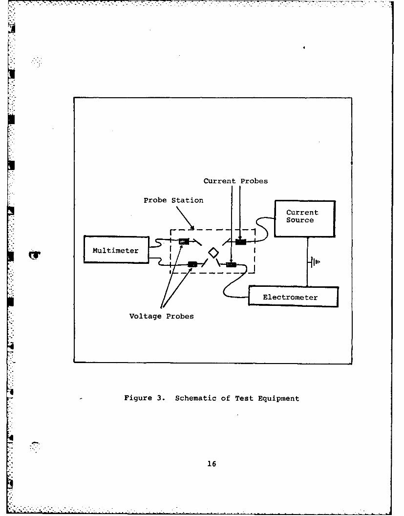
3 Schematic of Test Equipment . . . . . . . . 16
4 Illustration of Finished Samplewith Contacts ........... .. . 23
5 Test Patterns Used to Evaluate SpecificContact Resistivity . . . . . . . . . . . 25
6 Probe Positions on Test Patterns . . . . . . 28
7 Expected Graphical Results . . . . . . . . . 31
8 Misalignment of Metal Contacts and Mesa . . 37
9 Resistance Versus Distance Plots ofExperimental Data . ........... 38
10 Plot of vs Annealing Temperature .... 39. 0c
11 Plot of RSH vs Annealing Temperature . . . . 40o.H
12 Plot of RSH vs Dose .. ........ . 43
13 Plot ofp vs Dose ............. 44. 0c
14 Proposed Ohmic Contact Test Pattern . . . . 48
p."
I°-
List of Symbols
EF - Fermi Energy Level
#B - Potential Barrier Height
- - Metal Work Functionm
- Semiconductor Work Function
W - Space Charge Region
. -Electron Affinity
Si - Current (amp)
J - Current Density (amp/cm2
LT - Transfer Length (cm)
1 - Spacing Between Contacts (cm)
m - Slope (f/cm)
2PC Specific Contact Resistivity (f-cm2)
R - Resistance (0)
R - Contact Resistance (0)
RSH - Sheet Resistance (/3)
Sx - Standard Deviation
t - Degree of Certainty for a Given Degree of Freedom
p - Predicted Range
- A Mean Value
x - Length (cm)
x C - Contact Length (cm)
x - Apparent Transfer Length (cm)LT
.z - Contact Width (cm)
vi
. . . . . . .

AFIT/GEP/PH/82D-8
Abstract
A study of fabricating a low resistant contact on
. implanted n-type GaAs was conducted. Ion doses of
l x to 1cx and annealing temperatures
of 700 0C to 9000C were tesled in order to achieve the lowest
specific contact resistivity. Experimental results show
that a low specific contact resistivity of 2.78 x 10
can be obtained on GaAs layers which have been formed by ,'-'S1--_ (3 x :i014i ) implantation in undoped semi-insulating
daAs annealed at 850*C using an oxygen-free chemical vapor --
deposited Si3N4 layer as an encapsulant followed by subse-
quent deposition of AuGe/Ni ohmic contacts. Recommendations
are discussed concerning further studies and a design for a
new contact test pattern which would improve the degree of
,accuracy of resistivity measurements.
K. /65 - " . . .'Y ;
vii

.W _V Z 2 . ...*. . .
1, ,
STUDY OF OHMIC CONTACTS ON
Si 2 8 - IMPLANTED GaAs
I Introduction
In the world of high. speed electronic device applica-
tions, interest has developed in producing devices using
gallium arsenide (GaAs). The problem lies in fabricating a
good reliable low-resistance contact to such devices. An
'ideal ohmic contact allows current flow in either direction
without any resistance, however such an ideal contact is not
always possible to produce in a working environment. A
potential barrier between metal and semiconductor interface
" is nearly always present to make the contact less than ideal
(Ref 1). A contact may still be considered ohmic if the
resistance is small and the voltage drop is linear with the
changes in the current flow. Numerous studies have been
made on minimizing the effect of the barrier and reducing
the contact resistance (Ref 2, 3, 4, 5).
The ohmicity of a contact is often evaluated in terms
of its specific contact resistivity, pc (Ref 5, 6, 7); the
units of P being in -cm2. Ideally, pc = 0, but normally
p.i -is sr_ .L. A low-resistance ohmic contact has a p
of typically , however even lower resistances are
desired.
.. .. . . , .. .. ., , ., -. . .. .. .. , .,• .. . -. , . .-. . .. . . . ,.. °. . .,,.. •- , - .

Research on the theory of metal-semiconductor inter-
faces and their current transport characteristics are
usually considered to have begun with work of Mott (Ref 8)
and Schottky (Ref 9). The initial experimental work on
developing alloyed typed ohmic contacts to GaAs was performed
by Cox and Strack (Ref 10). Since that time, various methods
for fabricating ohmic contacts have been examined. The usual
technique alloys a Au-Ge contact mixture into the GaAs sur-
face. The Ge is believed to move into the GaAs surface and
creates a highly doped region which forms a thin space charge
layer that electrons can tunnel through. Usually thermal
alloying is performed, but laser annealing and electron beam
annealing (Ref 11) has gained current interest. As a means
to reduce the contact resistance, ion implantation has been
tried with success (Ref 3, 4, 12). Various ion species have
been studied such as Si, Se and (Se +Ge) that have produced
7 2contacts with reported resistivities of -3 x 10 -7-cm
(Ref 3).
More importantly, a dependable means of fabricating a
low-resistance contact needs to be developed since so often
an ohmic contact is fabricated but then cannot be reproduced
(Ref 5, 13). One objective of this work is to obtain pre-
dictable results from a fabrication process in particular,
the process of ion implantation. As a second objective,
this research sought to minimize p c by varying implantation
doses and the annealing temperatures. The implantation of
2

ions serves to increase the number of carriers in the mate-
rial and therefore to reduce the contact resistance. The
annealing process activates the implanted ions by placing
the ions in lattice sites within the crystal structure.
This thesis presents a brief background on the theory
surrounding ohmic contacts and resistivity along with a
mathematical development in Section II. Section III gives
a description of the equipment used in the research; plus
the procedure for preparing the sample, taking the measure-
ments, and performing the calculations. The data and results
are presented in Section IV. This paper concludes with
recommendations for further studies in Section V.
3

II Theory
Before any discussion of contact performance and ohmic
contacts, one must have a clear meaning of the word "ohmic".
To define this term, the structure of the metal-semiconductor
(MS) interface has to be considered. The nature of ohmic
contacts and specific contact resistivity will be discussed
in this section. Finally, a mathematical approach that leads
to solving for the contact resistivity will be presented.
Ohmic Contacts and Resistivity
' . When a metal and semiconductor are joined, a potential
barrier is formed at the interface. Figure 1 shows the band
diagram of a MS contact on a moderately doped semiconductor.
This type of barrier is referred to as a Schottky barrier.
In the figure, E and E represent the semiconductor con-c v
duction and valence bands, respectively. The Fermi energy
level is EF. The potential barrier height is given by *B
and the space charge region width is W.
Classically *B is defined as
. B = fm - s
where f is the metal work function and X is the electronm so
affinity of the semiconductor (Ref 14). If fm > s where
is the semiconductor work function, the barrier of
4
U. u
a.z 0 0
U *r4
0'
z .a
0*c
2: VF-ti: M I~ ~. E4
I '~'.~J a
UA I"LuJ
00
U Z.I' 2: W
I- CI
Figure 1 results. This barrier impedes the current flow and
even for low values of current, large voltage drops appear
across this interface which can result in a large contact
resistance.
If Om < *s S B can become zero or even negative. In
such a case, the current sees essentially no resistance
since no barrier exists. An ideal contact is defined as one
that has zero contact resistance. The most desirable con-
tacts are ohmic contacts with zero contact resistance. How-
ever, most practical MS combinations do produce a barrier
and therefore a less than ideal contact. Obviously when
fabricating ohmic contacts onto devices, the goal is to have.
a smaller voltage drop across the contact interface than the
voltage drop across the bulk region of the device. Thisminimizes the presence of the contact so that the contact
does not affect the performance of the device. The I-V
response of the contact should be linear as well. In this
case, the description of "ohmic" becomes a relative one,
being compared to the bulk resistance of the device.
A more quantitative way to describe ohmic contact
performance is in terms of specific contact resistivity,
2PC' ,which is given in units of f-cm . The definition of P c
lumps together the effects of the contact interface into a
single distributed resistance. If the I-V response of the
interface is linear, the value of pc is applicable over all
voltage drops. If the I-V response is non-linear, then the
6
value is applicable only at one particular value of I and
V. Lower values of Pc are preferred.
When contact current flow is perpendicular to the inter-
face, the resistance of a contact of a given area A can be
Pstated asr.-. P
c A
and voltage drop across the contact is calculated from
V = I . (2)
For current flow in a planar contact, current flow is not
strictly perpendicular therefore Eq. (2) cannot be applied
directly. A different method must be used to relate V to
I and pc (Ref 6, 7). In such cases, the concept of pc is
still a valid and convenient way to characterize the per-
formance of the contact. Therefore a contact with suffi-
ciently small P values could be called "ohmic". Normally
contact that has a Pc in the range of 10-3 0-cm2 to 10- 6-cm2
is considered an ohmic contact.
One means of reducing the Pc is to heavily dope the
semiconductor which causes the barrier slope from Figure lB
to become steeper and W to be reduced. For values of W on
the order of a few lattice spacings, electrons can quantum
mechanically tunnel through the barrier when a voltage is
Ki applied and give rise to a current. The tunneling currents
can be quite large and create a contact with a very low
' "resistance. Ion implantation is used in the same manner.
7

The implantation reduces W and produces a contact with a low
PC"
A second method used to reduce the potential barrier is
ion implantation. This is the method employed by this study.
Ions are implanted into the semiconductor to increase the
number of carriers in the material. An annealing process
follows which activates the implanted ions by placing the
ions in lattice sites. Consequently, both the implantation
dosage and the annealing temperature affect the Pc"
Mathematical Development
By definition, the specific contact resistivity is
.., given by
where PC = specific contact resistivity.
V = voltage
J = current density
One of the methods of determining pc is to use a transfer
length measurement. In this method the actual measured
quantity is the transfer length, LT . LT is the distance
that the current has to flow under the contact before the
I fraction (1 - ifrac 1 is transferred to the contact.
If a transfer length test pattern is used such as the
K one in Figure 2 and a current is passed between the end
- contacts, the potential developed can be measured against
8

I , 010 00---
Mesa Edge
x=O
~ Metal Contact
z = 78 p.mx = 53 pim
Figure 2. Transfer Length Pattern
9

the distance x. In the ideal case, the potential Vo at x=0
should be zero, but in fact the potential Vo at x=O is not
zero due to the contact resistance R and the resistance ofi" C
the semiconductor active layer under the contact.
As the current passes through the conducting layer, a
voltage drop V(x) is due to the IR drop along the sheet
resistance of the layer. Or
S=z dV(x) >0(3
R SH dx
where z is the width of the contact. A plot of V(x) versus
x should give a straight line with a slope of[IRSH]. RSH
is calculated from the slope since I and z are known.
Eq. (3) is valid as the current goes through the active
layer. As the current reaches the contact some of it is lost
to the contact because of pc" Then the potential is given by
V(x) = V(o)exp (L), x < 0. (4)
From Eq. (4), LT is defined as
which can be also written as
Pc RsHL2 " (5)
Experimentally, LT is determined from the linear extrapola-
tion of the line to V=0. Rc is given by
Rc V(o) (6)Rc I6
10
.........................-.......... .. .. ............... ._ 2: .. :2 _ . : ; .: ...... .' . ...... .: . 2, . , ..

The previous equations were developed based on an
assumption that the contact length is infinite. The contact
is assumed to be infinitely long if LT is much smaller than
the contact length xc If the contact is not infinitely
long then a more exact analysis must be performed. Wigen
et al. (Ref 5) have done an explicit derivation of this
case. The difference is the finite and infinite treatment
lies in the boundary conditions used. In this treatment,
Wigen proceeds as follows:
The current lost to the contact at any point X is
dI(X) = V(A) zdX . (7)PC
All the current enters the contact, therefore I must goTOT
into the contact between A =x and X =0.,." C
,'= (X)= fc v(X) zdXTOT j 0.,
and this gives the boundary condition on V(X).
If Vo represents V(A=O), a constant, the voltage V(W)
at any point O<a<xc, is the sum of V and the total RSHdI
voltage drop up to that point.
R SV(W) = V0 + J dI(X) -z -X)1
0
Substituting from Eq. (7), the above equation can be re-
written as
V(v) " + RAXIR11o -
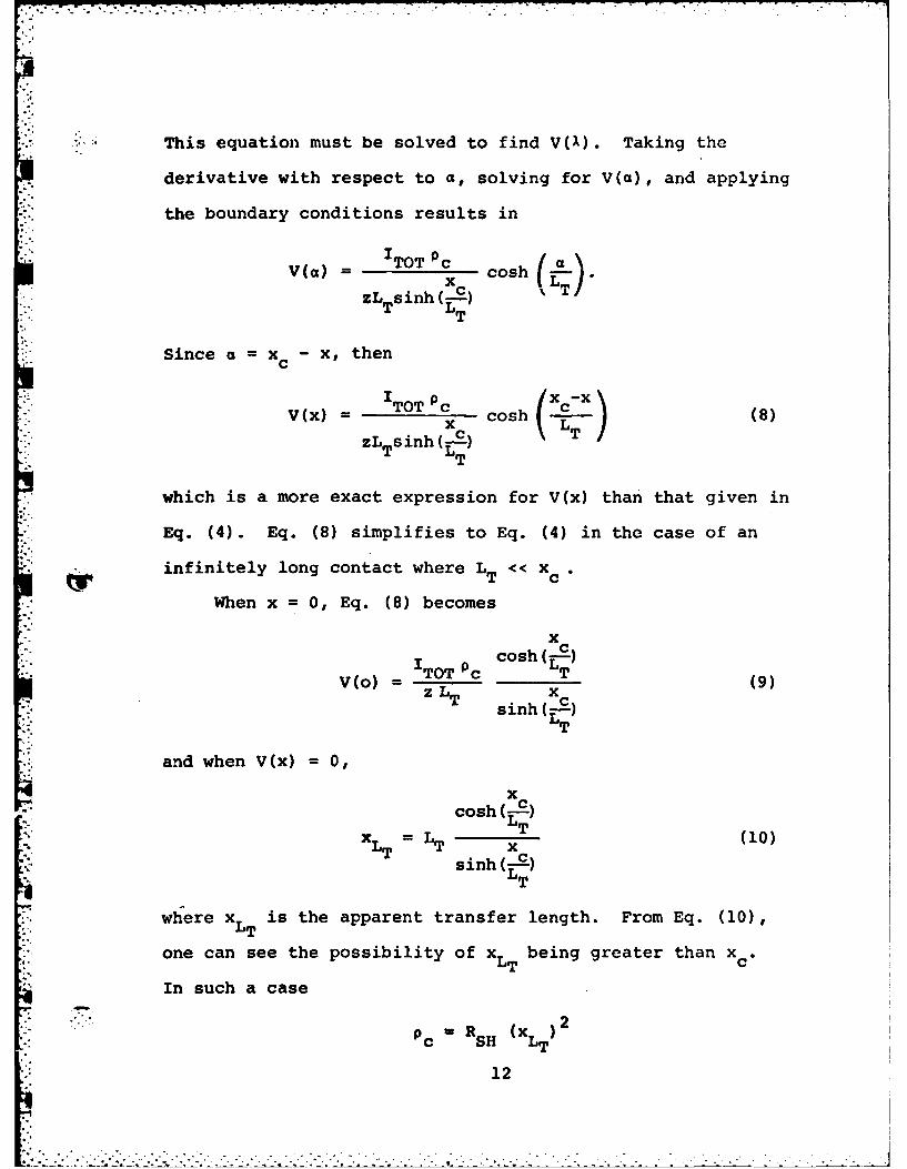
This equation must be solved to find V(A). Taking the
derivative with respect to a, solving for V(a), and applying
the boundary conditions results in
zL:sinh(ES ) I
Since a x X x, then
V(x) =cTOTh (8)
.xX Ld
T LT
which is a more exact expression for V(x) than that given in
Eq. (4). Eq. (8) simplifies to Eq. (4) in the case of an
infinitely long contact where LT x c
When x 0, Eq. (8) becomes
x
cc
cosh (81
V(o) TOT c T (9)z L xT.sinh
T
and when V(x) = 0,~x
(-:_ " cos
x L = LT T (10)LT Tx
sinh (-S)L T
where x is the apparent transfer length. From Eq. (10),LT
one can see the possibility of x being greater than xc -LT
In such a case
p R (xC SH LT
12

would be in error. To solve for the correct expression for
Pc' XLT and xc are used to calculate the proper value of LT.
Eq. (10) is rewritten as follows:
x cosh ( 1
LT TJxc siix'" 1 -) sinh( ( )
T T
When Xc/LT << 1, such as in the finite contact case, then
I- -i+ ! . ~cosh (T
LT
and
X xsinh (C) -C
T T
Substituting these expressions into Eq. (9), an expression
for P is obtainedC
PC v(o) ZXCc= -- (z xc) (11)
cIi~i ITOT
Eq. (11) is valid when the contact cannot be considered
infinite. A finite condition exists when pc is large
compared to RSH, making the voltage drop in the contact due
mostly to Pc" The contact may be taken as infinite if
x: -- > 2 (12)
LT
or substituting in for LT,
1/2"~ "::' c-.- _ 2
13
- . .. -

* Determination of Specific Contact ResistivityFrom the mathematical development, the approach to
determine p cbecomes evident. A constant current is passed
through two contacts and the potential created is measured
against the distance x. A straight line can be plotted
through the experimental points using a least squares
technique. RSH and Rc can be evaluated mathematically. LT
L-.- is extrapolated from data to evaluate P . If the contact.: C
satisfies the infinite condition
x xc >c > 2
LT
then pc is determined fromrC
PC Rc SH L TFor an ohmic contact, the p c should fall in the range of
10 10 - -cm An ultra low specific contact resis-
tivity is one that is less than 106 0-cm2 .
14
A..,..- - .
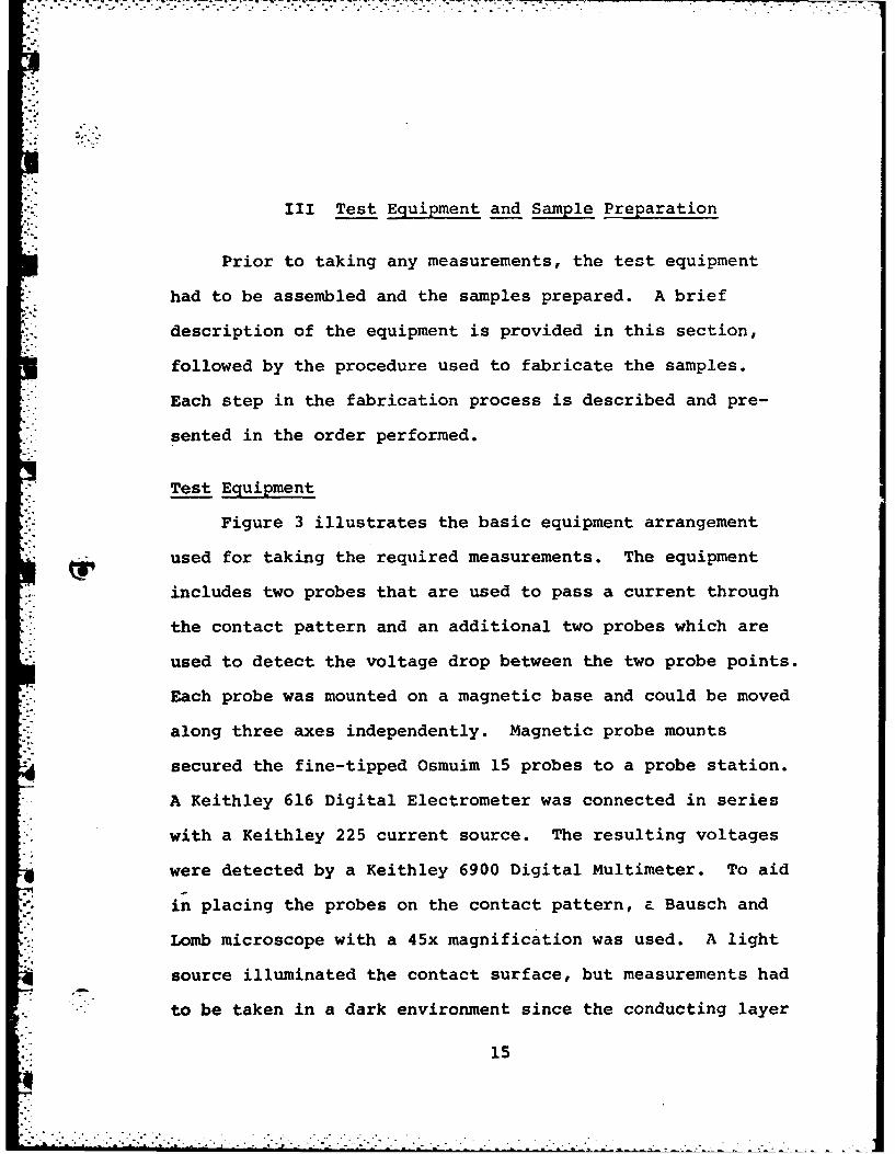
III Test Equipment and Sample Preparation
Prior to taking any measurements, the test equipment
had to be assembled and the samples prepared. A brief
description of the equipment is provided in this section,
followed by the procedure used to fabricate the samples.
Each step in the fabrication process is described and pre-
sented in the order performed.
Test Equipment
Figure 3 illustrates the basic equipment arrangement
used for taking the required measurements. The equipment
includes two probes that are used to pass a current through
the contact pattern and an additional two probes which are
used to detect the voltage drop between the two probe points.
Each probe was mounted on a magnetic base and could be moved
along three axes independently. Magnetic probe mounts
secured the fine-tipped Osmuim 15 probes to a probe station.
A Keithley 616 Digital Electrometer was connected in series
with a Keithley 225 current source. The resulting voltages
were detected by a Keithley 6900 Digital Multimeter. To aid
in placing the probes on the contact pattern, a Bausch and
Lomb microscope with a 45x magnification was used. A light
source illuminated the contact surface, but measurements had
. to be taken in a dark environment since the conducting layer
15
4 . ,,
Current Probes
Probe Station
Multimeter
Voltage Probes
Figure 3. Schematic of Test Equipment
4-16
[:16

.. -
is optically sensitive. Thus when measurements were taken,
the light source was turned off and a large black drop cloth
was used to cover the entire probe station.
Sample Preparation
The experimental samples were fabricated from undoped
GaAs substrates, Material Research, stock number A555/R.
These substrates were found to be of fair quality. In order
to prepare a sample for testing, the sample had to be
cleaned, free-etched, implanted, pyrolytically capped,
annealed, and mesa etched before the metal contact could be
deposited and alloyed. Each of these steps will be covered
in detail in this section.
Ion Implantation. The implantation dose was used as a
parameter in this study. All samples were implanted with
28Si - ions of a fixed energy, 100 Key, but were implanted
at different doses. The doses used in this study were
5 12 cm- 14 -25 x 102 1 x 10 cm
13 -2 14 -21 x 10 cm 3 x10 cm13 -215 -23 x 1013 cm-2 1 x cm
and all samples were prepared under the supervision of
Dr. Park.
- Sample Cleaning. The cleaning of the sample is
necessary prior to any further processing. First, the
4sample was washed and swabbed with basic-H solution, then
rinsed with de-ionized (DI) water. Next it was subjected
17
to a chemical wash of trichloroethylene, acetone, and
methanol, followed by a second rinse of DI water and blown
dry with nitrogen.
Pyrolytic Encapsulation. The encapsulation of the
implanted sample is necessary to prevent any losses of
either dopants or host material atoms from the sample
surface during annealing. All encapsulations were performed
by Charlie Geesner of the Avionics Laboratory. Just prior
to capping, the sample was soaked in HC1 acid for one
minute after which a layer of Si3N4 was deposited on the
surface of the sample using a pyrolytic technique.
Annealing. The annealing was done in a furni:ce in A-1
environment of flowing H2. For the purpose of tha±s experi-
ment, the annealing temperature was first fixed at 850°C for
all doses, and then varied from 7000 - 900 0C for two fixed
doses. A summary of the annealing temperatures and doses
for the samples which were prepared is given in Table I.
In general, the furnace was allowed to heat up to the de-
sired temperature after which, the sample was placed in the
furnace and was annealed for 15 minutes. Following the
annealing time, the sample was cooled to 400 0C before it
was removed from the furnace.
Removal of Si3N4 Cap. Once the annealing process was
completed, the Si3N4 cap was removed. The sample was soaked
in HF for three to four minutes until the cap lifted off.
Immediately afterwards, it was rinsed with DI water and blown
dry.'" 18*, ' " --, ..* ; 2 " i . . i. i . ? ; ? --- . - - .. . ' .?-. :... . ...-... ... . ; ..,.. ........ ..

TABLE I
Prepared Samples
Dose Annealing Temperature-2(cm_) 700 0C 800°C 8500C 900 0C
5 x 1012 X
1 x 101 3 X
3 x 1013 X X X X
lx 10 X
3 x 101 4 X X X X
1 x 10¹⁵ X
Mesa Etching. This process created a mesa region where
the metal contact was deposited. It served to isolate the
numerous contact patterns from current leakage. The etch
must be deep enough to go beyond the depth of implantation,
otherwise the applied-current path will seep around the
contact pattern. If the current path is not perpendicular
to the contact pattern, the mathematical analysis of the
data fails.
The mesa etch process began with a voltage breakdown
dtest of the surface. One expects a low breakdown since the
surface should be highly conductive. The sample was cleaned
in the same fashion as was described before. Next, the
sample was baked-out at 200*C for 30 minutes in an N2 ambient
oven. The HMDS and AZ1470 photoresist (PR) were then applied
19
. " to the samples followed by a pre-bake at 700C of 20 minutes.
Using a photographic mesa mask, the region to be etched
off was exposed to ultraviolet light. Development takes 30
seconds in AZ351 developer. At this point, the exposed
areas of the PR were lifted off so that the sample could be
post-baked at 100°C for 30 minutes to harden the remaining
PR. The actual etch was done with HF:H 0 :H 0 (1:1:8), which2 2 2o
etches off about 100 A per second. The samples were allowed
to soak in the HF solution for one minute to etch off about
0.6 um.
The remaining PR was removed with acetone after which a
second voltage breakdown test was performed. This test was
performed to determine the breakdown of the etched away
portion of the sample, which should be a nonconducting sur-
face. The breakdown voltage should be significantly in-
creased as was the case for this work where the breakdown
voltage went from 5V to 50V. Finally, the mesa step height
was measured to check the etch depth.
Deposition of AuGe/Ni. At this point, the sample was
finally ready for the deposition of the metal. The sample
was cleaned and baked-out as previously described. The
HMDS and PR were applied, and then the sample was baked at
700C for 10 minutes. The contact pattern mask was aligned
to the mesa and the sample was exposed to ultraviolet light.
4Following the exposure, the sample was soaked in chloro-
benzene for 4.5 minutes and baked at 700C for 15 minutes.
20

Development took 2 minutes and resulted in the removal of
the PR where the contacts are desired. Immediately before
deposition, the sample was soaked in dilute HF for five
seconds to remove any oxidation on the surface. The actual
deposition was done by technician Carol Travanski. The
excess metal was lifted off by soaking the sample in acetone
and using a gentle ultrasonic bath to shorten the soak time.0
The 2000 A thick metal contact was composed of AuGe/Ni which
consisted of 25% Ni and 75% AuGe, where 88% (by weight) of
the AuGe is Au.
Alloying. The metal contact of AuGe/Ni must be alloyed
to minimize the contact resistance. The usual alloying
temperature varies from 400 to 450*C at different intervals
of time, the higher the temperature, the shorter the time.
In general, the lower temperature will produce the most
uniform contact but not the lowest contact resistance. A
higher alloying temperature results in a less uniform surface
but a lower resistance, and too high of a temperature might
cause a loss of As in the conducting surface. In this study,
an alloying temperature of 450 0C was used for 30 seconds.
The furnace was pre-heated to about 530 0C after which
the sample was pushed into the furnace. After approximately
2.5 minutes, the sample would reach 430 0C and at this point
the 30 second alloying time would begin. The sample was then
4 partially pulled out of the furnace and allowed to cool to
approximately 2000C before being removed completely.
21
Throughout the alloying process, the furnace was filled with
flowing Ar gas.
An illustration of a finished sample with contacts is
shown in Figure 4.
.2
:22

AuGe/Ni Contacts
Me a
Non-conductingSurfacee
~ Metal
Figure 4. Illustration of FinishedSample with Contacts
23

IV Procedure
Two types of test patterns are commonly used to
evaluate contact resistance, Rc, and contact resistivity,
PC Both patterns follow the same theory and methematical
development. Any difference in the analysis of the data is
* ~. noted in this section. Both patterns make use of the
transfer length concept. However, in order to distinguish
between the two designs, the patterns will be designated the
ohmic contact pattern and the transfer length pattern. These
were the names found in literature for the patterns. The
geometry of each pattern in shown in Figure 5.
The ohmic contact pattern (Figure 5b) consists of seven
rectangular metal contacts. Each pad is separated from the
adjacent one by a different length: 3.39 pm, 8.67 pm,
13.69 pm, 18.91 pm, 23.99 pm, and 29.14 prm, respectively.
The transfer length pattern (Figure 5a) has two large
contact pads on the ends. Between the two pads are six
equally spaced voltage pick-off strips. The ohmic pattern
has a higher degree of accuracy while the transfer length
pattern provides ease of measurement.
The procedure used to take measurements, calculate
RSH, RC, LT, and PC, and compute the error bars will be
presented in this section.
24

'7 /
b. Ohc Cotc Paterne
Figrea. Trasfeet Pattern e oeaut
SpcfcCnac eitvt
25

1:4
Measurements
Measurements are obtained by using a four-probe method.
Before any measurements are taken a couple of checks must be
made to ensure the contact is ohmic and the conductive
surface is isolated. This section will describe how the
checks and the measurements are made.
If the mesa etch is not deep enough, the applied
current will diffuse around the mesa, therefore each pattern
must be isolated to take proper measurements. In other
words, only the mesa must contain the highly conductive
surface. To check for current leakage, two patterns are
selected that are positioned end to end. One current probe
is placed on each pattern forcing the current to pass through
an etched portion of the sample. By measuring the voltage
drop between the patterns, one can determine if the etch
region is still conductive or non-conductive. The resistance
between patterns should be significantly higher than the
resistance measured within a pattern. Often the current
will be difficult to maintain between patterns, indicating
good isolation.
All contacts must be ohmic. The traits of an ohmic
contact are a linear relationship between the voltage and
the current, and a non-preference to current polarity. To
check for the linear relationship, merely send various
currents through two contacts and note the respective
voltage drops. Twice the current should have twice the
26
• ' , - , -. e- - - , --, - - -. . . . . - - ;,,...; -..-,, - -,, .,. ,,. ,..--.-,, ,. - - . ,- ,. .- -- I

-4
voltage drop. Non-preference to polarity means the absolute
potential difference will not change as the current goes
from positive to negative. This trait can be readily
checked.
Once the pattern was confirmed as being isolated and
the contact being ohmic, measurement of the contact resist-
ance can begin. All measurements were taken using a four
probe method. This method uses two current probes and two
voltage probes. The advantage of this method compared to a
two probe method is that the current probes' resistance is
eliminated from the voltage readings.
When using the transfer length pattern, the current
probes are placed on the large end pads. The current passes
through the entire pattern and the cuzrent probes are never
moved. One voltage probe is fixed on one of the end contact
pads while the second voltage probe is moved from one finger
contact to another.
Figure 6a illustrates the four probe method as it is
applied to the transfer length pattern.
For the ohmic pattern, none of the probes are fixed.
Current probes are set down on two adjacent pads and the
voltage probes are positioned in a similar manner. The
ohmic pattern always has a current probe and a voltage probe
on a pad. Figure 6b shows the positioning of the probes on
the ohmic pattern.
27

f ixedI probe V probe fixed
ItI. . . . . . . i . . . . ..* * . S
;,: I I V= 0
i n n
n-type conducting layer
substrate
.:22 .a. Transfer length Pattern
;)'. _-type conducting layer.
~substrate
b. Ohmic Contact Pattern
Metal
Figure 6. Probe Positions on Test
Patterns
28

. .. ... .... . . '- . - - .. - -. i i - i
-* Calculations
For a given pattern, resistances are measured for
various distances through the conductive material. The
resistance is determined from Ohm's Law:
:" VR=-
where R is the resistance, V is the voltage, and I is the
current. The distance through the material, x, is the
separation between contact points.
A plot of R versus x should yield a linear relationship.
A non-linear relationship would suggest the contacts were
not ohmic. The straight line can be plotted through the
data points using a least square fit. Once a linear fit has
been made to the points, the slope is easily determined.
The sheet resistance, RSH, is computed from
RSH = z • m
where z is the contact width (cm), and m is the slope of
the line (A/cm).
The intercepts of the line give valuable information.
The y-intercept is equal to twice the co..act resistance,
Rc, while the x-intercept is twice the transfer length, LT.
This statement is true for the ohmic contact pattern. Since
the transfer length pattern is measured differently, y(o) is
equal to Rc , and x(o) is equal to LT. Regardless of which
pattern is used, the slope remains the same.
29

Physically, the slope and R must be a positive value.
The absolute value of the x-intercept is used for LT. If
the data should yield a negative y-intercept, then the
results are invalid.
To compute p c, the specific contact resistivity, one
needs to know if the current sees an infinite or finite
contact. A contact may be considered infinite if
xC > 2 LT
where xC is the length of the contact. All measurements
taken in this work met the above condition. Therefore, all
the contacts could be considered electrically long or in-
finite.
If the y-intercept is positive and the contact is in-
finite, then p is computed from
~2PC R RSH L T2
Figure 7 depicts the expected graphical results from measure-
ments using the two test patterns.
Error Bars
The error bars are computed from a statistical analysis
of the data. On a given device, a large population of
patterns are available. Close to 120 ohmic patterns and
60 transfer length patterns are on each device. A sample
of the patterns are selected to represent the whole.
-- Usually 9 - 12 patterns were measured on each wafer.
30

4.)1
04 4
40) 1
41) x-1
04 W: 04Ut
0 i
r i
(8W40)U 4JW.IS~
4P4
4P

. . Statistically, the predicted range is derived from
3f x t (13)
where x is a mean value, Sx is the standard deviation, n is
the number of measurements taken, and t is the degree of
certainty for a given degree of freedom. All error bars
shown in this study contain a 90% degree of certainty. In
other words, the true value of the measurement has a 90%
probability of falling within the range indicated by the
error bars. t values were taken from a statistical chart
(Ref 15: A-9).
32
V Results
All samples were checked for the electrical isolation
of an individual pattern. This initial step confirmed the
mesa etch was sufficiently deep. Next, each sample was
tested for contact ohmicity. All the samples had ohmic
contacts except one: the sample that was implanted to a
12 -2dose of 5 x 10 cm and annealed at 8500C. Even after
re-alloying, this sample did not form an ohmic contact. As
-. a result, no data could be obtained from this sample.
Following these initial tests, measurements could begin to
be taken. Immediately two problems arose. Each sample had
the two test patterns on it. A discrepancy developed between
the findings of each pattern for the same sample. The two
patterns were yielding values of pc that were orders of
magnitude apart. Secondly, when some of the data points
were plotted out, the y-intercept would have a negative
value. Clearly, a negative intercept indicates a negative
contact resistance which is not physically possible. Both
of these problems will be discussed further in this section,
and the findings of this study will be presented.
Discrepancy Between Patterns
The two test patterns provide two ways to measure the
same values. The question that needed to be answered was
33| "
which pattern gave the most reliable results? To determine
this, Hall measurements were taken for samples implanted13 -2 14 -2
with three different doses, 1 x 10 cm 1 x 10 cm ,
and 1 x 1015 cm -2 all annealed at 8500 C. The Hall measure-
ment provided very accurate values for the sheet resistivity,
RSH. Comparing the Hall value of RSH to the values deter-
mined from the two patterns, one could gauge which pattern
was yielding better results. The ohmic pattern consistently
provided better measurements. The reason the transfer length
pattern was inaccurate is still unclear.
The transfer length pattern measures voltage drops over
a distance of 400 pm, with the first data point at a distance
of 53 pm and all other points 56 pm apart thereafter. The
resistance across the total length varies from 1 - 1000 0,
but the value of R to be determined is only about 20.
Therefore, the resolution near the y-intercept is poor and
the Rc value is very sensitive to slight changes in the
slope of the R versus distance curve. On the other hand,
the ohmic pattern uses a maximum distance of 30 pm and pro-
duces resistances varying from 1 - 100 a. The ohmic pattern
would seem to have a better resolution near the y-intercept
because of the smaller range of the plot. In addition, the
transfer length pattern has a y-intercept that is equivalent
to R, while the ohmic pattern's y-intercept is equal to
4 twice R . The ohmic pattern would probably yield a truer
value of Rc. Based on the above discussion, the ohmic
34
pattern was selected for all further measurements and the
transfer length pattern was abandoned.
Negative y-intercept
All measurements were taken from the ohmic pattern.
However, the results were not always acceptable. Often the
y-intercept would have a negative value which clearly
indicated a flaw in the measurement or the evaluation. The
pattern had been designed with spacings between the contact
pads of 5 pm, 10 um, 15 pm, 20 pm, 25 Um, and 30 pm. At
closer inspection the spacings did not turn out to be
increments of 5 Um. Photographs of the pattern were taken
using a high-power microscope. The separations between pads
* were measured from the photograph with a high-grade meter
ruler. The separations were found to be 3.39 um, 8.67 um,
13.69 um, 18.91 pm, 23.99 Um, and 29.14 Um. These new x
values significantly altered the plot. Virtually all
measurements produced y-intercepts with positive values by
using the new x values. Still, not all negative y-intercepts
were eliminated.
Once again, the failure of the measurements could be
related to the contact pattern or difficulties of determining
the correct R values due to the resolution problem. In thec
contact fabrication process, two masks are used: one to
create the mesa and a second to pattern the contact design.
_ The two masks must be manufactured so that the contacts lie
directly on top of the mesa, however the two masks made for
35

this study were not perfectly aligned. The pictures taken
of the contact pattern show how part of the metal contact
lies off the mesa (see Figure 8). The misalignment would
allow part of the current to flow around the contact instead
of entirely perpendicular to the leading edge of the contact.
Therefore, the contact/mesa misalignment would introduce
some error in all measurements, although such an error would
be slight.
Findings
The experimental data when plotted formed a straight
line. A typical plot of experimental data is given in
Figure 9. For all plots the correlation coefficient was
always better than 0.99. This would indicate that the bulk
resistance or RSH was behaving as it should and the ion
implantation could be considered uniform over the dimensions
of the pattern. Two variables were used in this study: the
implantation dose and the annealing temperature.
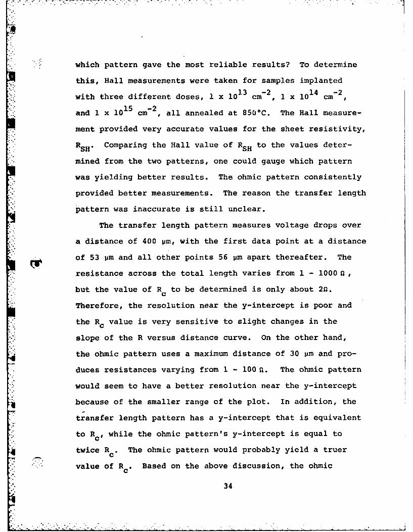
Fixed Implantation Dose. Figure 10 is a plot of c
versus annealing temperature for the two fixed ion doses.
Although an exact value of p c was difficult to determine
because of questionable intercepts, this plot reveals that
the annealing temperature over this range has virtually no
effect on p c Nevertheless, the annealing temperature did
alter the sheet resistance significantly. A plot of RSH
4 versus the annealing temperature is given in Figure 11.
36|4

a. Contact Pads 1 and 2
0..
bo Cotc Pas6 n
Fiur 8 MsainmntbMea ContactsPd and Mes
37

48
00
5 18 15 20 25 39
-4DISTANCE WOI CM)
a. Plot of a single dose over entire range
4.08
2.9
AL OES(M2
ExALLeta DOESata~ 2
38
m 0 lw
x x 0
0 U,I I ICD
* eON
w
r F-
NO
NN
LOI
WO-WHO) AIIAIISIS38i
39

if 0
C)) k
03 0
'.44
x xp
I 0
to 0
rr
I Ii i
0 03 co a
40.

This plot shows a definite decline in RSH as the annealing
temperature increases. The discrepancy between the annealing
behavior of pc and RSH may also indicate that determining pc
values with considerable accuracy is a problem. However, c
values for the dose of 3 x 1014 cm- 2 is generally lower than
13 -2those for the dose of 3 x 10 cm at all annealing tempera-
tures.
Fixed Annealing Temperature. For this portion of the
study, samples of various doses were annealed at 8500C for
15 minutes. Measurements were taken and a pc was computed
for each sample. A summary of the data obtained from the
samples at a fixed annealing temperature is given in
Table II.
Resistivity is calculated from the re.lation
P =R L2c SH T
where RSH is taken from the slope of the plot. RSH measure-
ments were quite consistent for all data taken from one
sample. The calculated RSH was compared to the RSH value
determined by Hall measurement. The comparison of the Hall
R and the experimentally derived RSH values is given inSH S
Figure 12. This plot shows that the experimental values
are in good agreement with the Hall measurements.
While the RSH values were very consistent for different
measurements on the same sample, the same could not be said
about the LT values. LT is determined by the x-intercept.
Often the x-intercept would vary by a factor of two or three.
41

TABLE II
Data Summary - Fixed Annealing Temperature
HALLDose RSH RSH Rc LT PC
(cm- 2 0/0) 0/0) W (xlO 5cm) (x10 7-cm2 )
1 x10 249.71 256.16 2.44 7.33 14.3
3x1 1 196.13 1.50 5.80 9.99
lxlO 1 188.75 191.90 1.46 5.82 6.57
143xl1 --- 166.47 .895 4.10 2.78
1 "xl0 1 5 155.10 164.13 2.30 10.6 18.8
Since LT drives the equation used to compute pc, pc values
are very sensitive to slight variations in LT-
Figure 13 is a plot of c versus dose. The points
shown use the mean value of p for that dose. The error
bars represent the range in which the true value for pc
could be found (90% certainty). The sample with the lowest
C value was the sample implanted at 3 x 10 cm 2 In
general, the greater the dose, the lower the p , until the
dose of 3 x 1014 cm-2 is reached. At that point, the trend
reverses itself and Pc increases with the dose.
The reasons that pc increases for the dose of 1 x 10¹⁵
-2cm are not well understood at present. Although the im-
planted dose is very high, the sheet carrier concentration
and R are not substantially improved from the values givenSH
for the 3 x 1014 cm-2 dose. This implies that significant
42
"* .. . . . -. '.* -4. .-2 -'_- . . . . . . . . ._" .. ' ' -. . . . - , ° .* *. ' "

U-))
(w w
:3 -T- 0i
w
a: Ew IJa
C9 w
z1- 0
U) -
'-4 0
m $34
43-

0.
..
-.-
wI-iL
LJ 0
0 V0
'4
444

-.- --
implantation damage may have remained for this sample, and
therefore pc is higher than that for the dose of 3 x 10¹⁴
-2i: cm.
Based on the findings of this work, the following trends
were observed. If the dose is fixed and the annealing tem-
perature is varied, no real change in pc occurs. However,
a definite change in RSH is observed: as the annealing
temperature is increased the sheet resistance decreases.
When the annealing temperature is fixed and dose is varied,
then a change in c is easily seen. As the dose increases,
the resistivity decreases until the minimum p is reached at14 -2
the dose of 3 x 10 cm , after which pc increases rapidly
with the dose. The minimum value of p that was obtained
is 2.8 x 10⁻⁷Q cm 2.
45
." -.

VI Recommendations/Conclusions
From the outset, this study sought to investigate the
effect of the ion implantation dose and the annealing tem-
perature on the specific contact resistivity. With the dose
held constant, the annealing temperature was varied over a
range of temperatures and pc was computed. While pc did not
change with the variations in annealing temperature, a change
was noted in the RSH values. RSH decreased as the annealing
temperature increased. The discrepancy in the annealing
behavior of pc and RSH may indicate that pc is not being
y determined accurately. However, the p c values for the dose
14 -2 13 -2of 3 x 10 cm were lower than those of the 3 x 10 cm
dose. When the annealing temperature was fixed at 850*C and
the dose was varied, a more definite trend was observed. In
* general the greater the dose, the lower the pc until the
minimum pc was reached at a dose of 3 x 014 cm-2 after
which an .increase in dose produced a sharp increase in pc"
This higher pc found in higher doses could be due to greater
ion implantation damage. The minimum pc value obtained was2.87 0 2 14 - 2
2.78 x 10 - 7 - cm for a dose of 3 x 10 cm annealed at
850 0C.
While the findings were useful, the experimental in-
sight gained proved to be the most beneficial result of this
work. These measurements had not been attempted before at
46

the Avionics Laboratory and unrefined experimental procedures
contributed to inaccuracies in measurements. Recommendations
for improving measurement accuracy are presented in the re-
mainder of this section.
The shortcomings of this work are directly related to
the contact test pattern dimension. The inability to obtain
accurate intercept values from the plot of experimental data
was caused by the relatively large dimensions of the pattern.
A higher degree of accuracy could be obtained if the
test pattern would be re-designed. The contact pattern shown
in Figure 14 has been proposed by Dr. A. Ezis. In the pro-
posed pattern the contacts are separated 2 um, 3 pm, 4 Um,
6 pm, and 8 Um. Given that
z = 70 pm
xc = 60 pm
14 -2Dose= 3 x 10 cm
PC 1 x 10 cm2
one can calculate the expected values of the intercepts.
From Figure 12, one can get
RSH 170 o/
so therefore
- RSSlope = RS =-2.43 f/pm
z
and/2
T =RSH = .243um
47

N N
I~iON
.r.
Ielax\
484
U
\\. "
,'-I
:1
O'
' .
481
nm -'- " " , ' , --7 K' ':7 7 J - _• • - -• , -I\

-.. .-
from which one obtains
R= (Slope) LT =.59 .
The proposed pattern does satisfy the infinite condition:
x > 2 LT
since
60um > .5p.m
For the proposed pattern dimensions the resistance measure-
ments would range from 0 to 20 a as x goes from 0 to 10 pm.
The y-intercept, which is 2 Rc , would be -1.20. The x-
intercept, which is 2 LT, would be -.5pm. These intercept
values should be easily determined by the proposed pattern
since the scale of the plot is greatly reduced.
Further improvements in this study could also be
*implemented. The semiconductor substrate was of fair
quality. Upgrading the quality of the substrate could
2. improve the consistency of the measurements. The slightly
inferior substrate could have contributed to experimental
variations in the data.
When the new mask is manufactured for the proposed
contact pattern, care needs to be taken to design a mesa
mask that is aligned to the pattern. Alignment eliminates
the concern of current flowing other than perpendicular to
the contact interface.
49

Lastly, the optics in the probe station needs to be of
a greater magnification. The greater magnification is needed
to see the contact pads and the separation between pads.
The optics could be improved by simply replacing the eye-
pieces with lenses of 20x or better.
The recommendations suggested in this section should
provide more reliable results. The frequency of question-
able intercepts should be reduced if not eliminated and a
greater degree of precision in p c measurements could be
achieved. The measurement method described in this work is
a simple experimental means of determining RSH, Rc, LT and
P" With the modifications given in this section, the
p measurements could be quite accurate and the results easily
reproduced.
2 50

K
Bibliography
1. Yu, A. Y. C. "Electron Tunneling and ContactResistance of Metal-Silicon Contact Barriers," SolidState Electronics, 13: 239-247 (1970).
2. Berger, H. H. "Contact Resistance and ContactResistivity," Journal of Electrochemical Society:Solid State Science and Technology, 119; 507-514(April 1972).
3. Inada, Taroh, and Shigeki Kato. "Ohmic Contacts onIon Implanted n-Type GaAs Layers," Journal of AppliedPhysics, 50(6): 4466-4468 (June 1979).
4. Ohata, Keiichi, Tadatoshi Nozaki, and Nobuo Kawamura."Improved Noise Performance of GaAs MESFET's withSelectivity Ion-Implanted n* Source Regions," IEEETransactions on Electron Devices, Ed-24(8): 1129-1130(August 1977).
5. Wigen, Philip E., Marlin 0. Thurston, Electron DeviceContact Studies. AFWAL-TR-81-1294. Wright-PattersonAFB, Ohio: Avionics Laboratory, May 1982.
6. Berger, H. H. "Models for Contacts to Planar Devices,"Solid States Electronics, 15(3): 145-158 (1972).
7. Schuldt, S. B. "An Exact Derivation of ContactResistance to Planar Devices," Solid States Electronics,21: 715-719 (1978).
8. Mott, N. F. Proc. Camb. Phil. Soc., 34; 568 (1938).
9. Schottky, W. Naturwiss, 26; 843 (1938).
10. Cox, R. H. and Strack, H. "Ohmic Contacts for GaAsDevices," Solid State Electronics, 10; 1213 (1967).
11. Eckhardt, G. "Overview of Ohmic Contact Formation onN-type GaAs by Laser and Beam Annealing," Laser andElectron Beam Processing Materials. New York:Academic Press, (1980).
12. Ehret, J. E., Y. K. Yeo, K. K. Bajaj, E. T. Rodine,G. Das, Characterization of Ion Implanted Semiconductors.AFWAL-TR-80-1171. Wright-Patterson AFB, Ohio: AvionicsLaboratory, November 1980.
51
". " , ' '- t . . ' " a ' " "h m °
" d " " :a . . ' "" . .T
"

13. Singh, Hausila P. "D. C. Properties of PassivatedGaAs MESFETS." Report for the Wright-Patterson AFBAeronautical Laboratories. September 1981.
14. McKelvey, John P. Solid State and SemiconductorPhysics. New York, Harper and Row, 1966, pp. 478-498.
15. Calculator Decision-Making Sourcebook. ProductSupplementary Book. Texas Instrument Incorporated,1977.
16. Beyer, William H. CRC Standard Mathematical Tables(25th Edition). Boca Raton, Florida: CRC Press Inc.,1978, pp. 509-510.
17. Brophy, James J. Basic Electronics for Scientists(3rd Edition). New York: McGraw-Hill Book Company,1977, pp. 2-4, 123-155.
18. Chang, I. F. "Contact Resistance in DiffusedResistors," Journal of Electrochemical Society:Solid State Science, 117; 368-372 (March 1970).
19. Hower, D., Hooper, S., Cairno, K., Fairman, C., andTremere, J. R. Metals and Semiconductors, New York,
or McGraw-Hill, 1975, pp. 178-181.
20. Kwok, S. P., M. Feng, Victor Eu. "Characterization ofUltra Low Ohmic Contact Resistance."
21. Yeo, Y. K. "Contact Resistivity," notes. Wright-Patterson AFB Avionics Laboratory, April 1982.
22. Yeo, Y. K. "Determination of the Specific ContactResistance," notes. Wright-Patterson AFB AvionicsLaboratory, August 1982.
23. Yeo, Y. K. "Hall-Effect/Sheet Resistivity (Van derPauw Method)," notes. Wright-Patterson AFB AvionicsLaboratory, January 1978.
52
q.A

: .. . . :::'; .:: - '?: . ; :-- ." > :. -.... • . . .. ' . :; .' .i 'i 'i:
I Is
Vita
Diane M. Fischer was born 22 February 1959 in Peru,
Indiana, the daughter of Curtis H. and Mary Fischer. After
graduation in 1977 from Zweibrucken American High School,
Zweibrumcken, Germany, she attended Angelo State University,
San Angelo, Texas. In May 1981 she was graduated with
honors with the degree of Bachelor of Science in Physics.
After receiving her commission as Lieutenant in the USAF,
she entered active duty in May 1981. Her first military
assignment was to the Air Force Institute of Technology in
the Graduate Engineering Physics curriculum.
Permanent address: 7971 Hanford WaySacramento, California
This thesis was typed by Mrs. Diane Katterheinrich
.-. n

UNCLASSIFIEDSECURITY CLASSIFICATION OF THIS I^rE .6 n Pa&,I rt..red)
REPORT DOCUENTATION PAGE READ INSTRUCTIONSBEFORE COMPLETING FORM
I. REPORT NUMBER 2. GOVT ACCESSION NO. 3. RECIPIENT'S CATALOG NUMBER
AFIT/GEP/PH1/82D-8 2 ____ ________
4. TITLE (and Subtitle) 5. TYPE OF REPORT & PERIOD COVERED.28
STUDY OF OHMIC CONTACTS ON Si - MS ThesisIMPLANTED GaAs
6. PERFORMING ORG. REPORT NUMBER
7. AUTHOR(e) 8. CONTRACT OR GRANT NUMBER(s)
Diane M. Fischer2Lt, USAF
9. PERFORMING CRGANIZATION NAME AND ADDRESS 10. PROGRAM ELEMENT. PROJECT, TASKAREA & WORK UNIT NUMBERS
11. CONTROLLING OFFICE NAME AND ADDRESS 12. REPORT DATE
December 198213. NUMBER OF PAGES
61
14. MONITORING AGENCY t AME & ADDRESS(iI dilferen from Controlling Office) IS. SECURITY CLASS. (of this report)
UNCLASS IFIED
ISa. DECL ASSI FICATION/DOWNGRADINGSCHEDULE
16. DISTRIBUTION STATEMENT (of this Report)
Approved for Public Release; Distribution Unlimited
17. DISTRIBUTION STATEMENT (of the abstract entered in Block 20, It different from Report)
IS. SUPPLEMENTARY NOTES -- 1.6.0 .A .AW Ow
;'+ D I ,~~~5 lot ;-" " -•.
Air FOC,
19. KEY WORDS (Continue on reverse side it necessary and identify by block number)
Gallium Arsenide Low Resistance ContactIon Implantation Specific Contact Resistivity
4 Silicon Implanted GaAs ResistivityOhmic Contact AuGe/Ni Ohmic Contacts
20. ABSTRACT (Continue on reverse side It necessery end Identify by block number)
A study of fabricating a low resistant contact on Si2 - implantedn-type GaAs was conducted. Ion doses of 1 x 1013 cm-2 to1 x 1015 cm- 2 and annealing temperatures of 700 0C to 900*C weretested in order to achieve the lowest specific contact resistivity.
S .-.. Experimental resul s show that a low specific contact resistivityof 2.78 x 10- fl-cm 2 can be obtained on GaAs layers which have beenformed by Si2 8 (3 x 1014 cm-2 ) implantation in undoped semi-
DD , FO."7 1473 EDITION OF I NOV I5 S3 OOSOLETE UNCLASSIFIED
SECURITY CLASSIFICATION OF THIS PAGE (KiIhen Date Entered)
* .-,. -...... .. . ... .. , . . ...,. - .+, . ++ .. . . .+ + . .+ .. . ...
UNCLASSIFIEDSECURITY CLASSIFICATION OF THIS PAGE(I-Th.n Data 1.nteped)
(continued)19. Transfer Length
Annealing TemperatureTransmission Line
(continued)20. insulating GaAs annealed at 850 0C using an oxygen-free
chemical vapor deposited Si3N4 layer as an encapsulantfollowed by subsequent deposition of AuGe/Ni ohmic contacts.Recommendations are discussed concerning further studiesand a design for a new contact test pattern which wouldimprove the degree of accuracy of resistivity measurements.
4.1
.6j r
Zj.
UNCLASSIFIED59(;UHITY CLASSIFICATION OF THIS PAGE(Mven Data Entered)