Embed Size (px)
Citation preview

Excited State Interactions and Management
in Organic Light Emitting Diodes
by
Yifan Zhang
A dissertation submitted in partial fulfillment
of the requirements for the degree of
Doctor of Philosophy
(Physics)
in the University of Michigan
2014
Doctoral Committee:
Professor Stephen R. Forrest, Chair
Associate Professor Max Shtein
Assistant Professor Vanessa Sih
Professor L. Jay Guo

© Copyright by Yifan Zhang
2014

ii
Acknowledgements
This thesis would have been impossible without the help from others. First, I
acknowledge my advisor, Professor Stephen Forrest for his intellectual as well as
financial support. Over the past years, I have been deeply inspired and energized by his
exceptional scientific insight and dedication towards the highest standard of work. I also
feel grateful that he gave me flexibility as well as trust in the projects I was on. I do not
know how to return his favor, but I will surely carry on the spirit of always thinking
critically and acting promptly.
Working in an interdisciplinary group with members from both science and
engineering backgrounds offered me an unparalleled opportunity to learn from my
colleagues. As my mentors, Stéphane Kéna-Cohen, Noel Giebink, and Xiangfei Qi
familiarized me with basic experimental as well as data analysis techniques. Michael
Slootsky offered me numerous critical suggestions, including editing my first research
paper manuscript, sharing with me a low temperature photoluminescence setup, and
teaching me how to design and fabricate printed circuit boards. Jaesang Lee assisted me
with device fabrication and characterization, which accelerated my progress in the final
project. Eva Ruff not only provided reliable support as the group administrator, but also
proofread this dissertation. I am also thankful to other group members for the enjoyable
time we spent in the lab, during group meetings, and beyond. Among them are Jeramy

iii
Zimmerman, Xin Xu, Richard Lunt, Kuen-Ting Shiu, Xuhuai Zhang, Guodan Wei, Greg
McGraw, Brian Lassiter, Kyle Renshaw, Xiaoran Tong, Kevin Bergemann, Xin Xiao,
Kyusang Lee, Xiaolong Hu, Nana Wang, Cedric Rolin, Olga Griffith, ByeongSeop Song,
Anurag Panda, Xiao Liu, Quinn Burlingame, Xiaozhou Che, Dejiu Fan, Yue Qu, Wen Yu,
Shota Nunomura, and the ones I forget to mention.
In addition, I acknowledge the contribution from Professor Mark Thompson at the
University of Southern California on some of my projects. Also, Dr. Julie Brown at
Universal Display Corp. offered experimental supplies and helpful suggestions that are
essential for part of this thesis. I also acknowledge Professor Max Shtein, Professor
Vanessa Sih, and Professor Jay Guo for serving on my dissertation committee.
My wife, Zhenxin, has been a constant inspiration during my graduate study. Her
support and tolerance are indispensible for me to complete this dissertation. I am also
grateful to my daughter, Annabelle, who has been growing up well in China. Lastly, I am
deeply indebted to my parents for their inexhaustible patience, and the enormous effort
they put into raising Annabelle.

iv
Table of Contents
Acknowledgements ............................................................................................................. ii
List of Figures ................................................................................................................... vii
List of Tables ..................................................................................................................... xi
List of Appendices ............................................................................................................ xii
Abstract ............................................................................................................................ xiii
Chapter 1 Introduction to Organic Semiconductors ........................................................... 1
1.1 The Unique Features of Organic Semiconductors .................................................... 1
1.2 Process and Deposition Techniques for Organic Materials ...................................... 5
1.3 Organic Light Emitting Diodes ................................................................................. 9
1.4 Organic Semiconductor Lasers ............................................................................... 13
1.5 Organic Solar Cells ................................................................................................. 17
1.6 Organic Thin Film Transistors ................................................................................ 19
Chapter 2 Physics of Organic Semiconductors ................................................................. 21
2.1 Electrical Properties of Organic Semiconductors ................................................... 21
2.1.1 Charge Injection ............................................................................................... 21
2.1.2 Charge Transport ............................................................................................. 25

v
2.1.3 Charge Recombination..................................................................................... 28
2.2 Photophysical Properties of Organic Semiconductors ............................................ 28
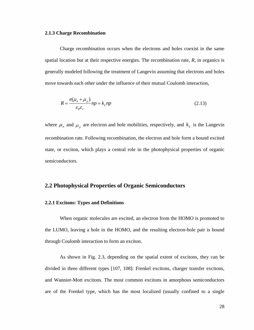
2.2.1 Excitons: Types and Definitions ...................................................................... 28
2.2.2 Exciton Transport............................................................................................. 35
2.2.3 Exciton Interactions ......................................................................................... 38
2.3 Exciton Interactions in Organic Light Emitting Diodes ......................................... 41
Chapter 3 Singlet-Triplet Annihilation in Fluorescent Organic Light Emitting Diodes . 44
3.1 Dynamics of Singlet-triplet Annihilation (STA) .................................................... 44
3.2 Transient Electroluminescence Turn-on Decay Due to STA ................................. 48
3.3 Use of a Phosphorescent Dopant to Reduce STA ................................................... 55
Chapter 4 Managing Triplets in Fluorescent OLEDs ....................................................... 58
4.1 Concept of Triplet Management ............................................................................. 58
4.2 Suppressed EL Turn-on Decay through Triplet Management ................................ 60
4.3 Enhanced OLEDs Efficiency through Triplet Management ................................... 65
Chapter 5 Organic Semiconductor Lasers (OSLs) With a Continuous-wave Threshold 69
5.1 Theory for Continuous-wave (CW) Lasing in OSLs .............................................. 70
5.2 Fabrication and Measurement of OSLs .................................................................. 73
5.3 Extended Lasing Duration in OSLs with Triplet Management .............................. 75
5.4 Observation of the CW Threshold in an OSL ......................................................... 82
Chapter 6 Triplet Contributions to Fluorescent OLED Efficiency ................................... 85
vi
6.1 Fluorescent OLEDs with both STA and TTA ........................................................ 86
6.2 Evaluation of the Role of Triplets in Fluorescent OLEDs ...................................... 94
Chapter 7 Triplet Annihilation in Phosphorescent OLEDs: Dexter-Mediated Triplet
Diffusion ........................................................................................................................... 98
7.1 Transient Photoluminescence in Phosphorescent Emitters ..................................... 99
7.2 Diffusion vs. Transfer Dominated Triplet Annihilation ....................................... 106
7.3 Emitter Design for High Brightness PHOLEDs ................................................... 110
Chapter 8 Controlling Triplet Dynamics to Extend the Operational Lifetime of Blue
PHOLEDs ....................................................................................................................... 114
8.1 Blue PHOLEDs Operational Lifetime: an Introduction ....................................... 115
8.2 Management of the Exciton Profile in PHOLEDs ................................................ 118
8.3 Ten-fold Improvement in the Lifetime of Blue PHOLEDs .................................. 129
Chapter 9 Future Work ................................................................................................... 135
9.1 A Singlet Fission Organic Coating for Photovoltaics ........................................... 135
9.2 Feasibility of an Electrically Pumped OSL .......................................................... 138
Appendix A Chemical Structures for Organic Molecules .............................................. 142
Appendix B List of Publications, Conference Presentations and Patents ....................... 146
References ....................................................................................................................... 150
vii
List of Figures
Figure 1.1 Structure of crystalline silicon and amorphous organic semiconductor tris(8-
hydroxyquinoline) aluminum (Alq3) ................................................................................... 2
Figure 1.2 Examples of urved and transparent OLEDs ...................................................... 3
Figure 1.3 Effect of material purity on OLED efficiency ................................................... 5
Figure 1.4 Setup for gradient sublimation purification of organic materials ...................... 6
Figure 1.5 Setup and operation of vacuum thermal evaporation (VTE) ............................. 6
Figure 1.6 Setup and operation of organic vapor phase deposition (OVPD) ..................... 8
Figure 1.7 Structure and operation of an OLED ............................................................... 10
Figure 1.8 Examples of OLED displays ........................................................................... 11
Figure 1.9 Chemical structures of organic semiconductor laser materials ....................... 14
Figure 1.10 Three different feedback structures for OSLs ............................................... 15
Figure 1.11 Structure and operation of an organic solar cell (OSC) ................................ 17
Figure 1.12 Curved OSCs installed on the bus shelters in San Francisco. ....................... 18
Figure 1.13 Basic structure of an organic thin film transistor (OTFT). ............................ 19
Figure 1.14 Characteristics of an OTFT ........................................................................... 20
Figure 2.1 Illustration of the barrier height for current injection from metal contact to
organics ............................................................................................................................. 22
Figure 2.2 The current density-voltage (J-V) triangle (shaded) formed by three charge
transport mechanisms in organics ..................................................................................... 27

viii
Figure 2.3 Three type of excitons determined by their spatial extent. .............................. 29
Figure 2.4 Ground state and excited state energies in the molecular configuration
coordinate .......................................................................................................................... 30
Figure 2.5 Emission and absorption spectra of anthracene ............................................... 32
Figure 2.6 Chemical structure and emission spectrum of platinum-octaethyl-phorphyrin
(PtOEP). ............................................................................................................................ 34
Figure 2.7 Annihilation between excitons considering both exciton diffusion and exciton-
to-exciton energy transfer ................................................................................................. 39
Figure 2.8 Calculated EQE for a fluorescent OLED with STA, and a phosphorescent
OLED with TTA ............................................................................................................... 43
Figure 3.1 Structure of a bottom emitting OLED on glass substrate ................................ 45
Figure 3.2 Simulated exciton density dynamics ............................................................... 48
Figure 3.3 Structures for the red and blue emitting OLEDs ............................................. 49
Figure 3.4 Setup for OLED efficiency and spectrum measurements ............................... 50
Figure 3.5 Transient electroluminescence (EL) of the devices ......................................... 51
Figure 3.6 Recovery of the turn-on peaks under double pulse current injection .............. 53
Figure 3.7 Delayed fluorescence from the devices ........................................................... 54
Figure 3.8 Electroluminescence transient of 1% Pt(TBPB) and 8% TBP co-doped with
the host .............................................................................................................................. 56
Figure 4.1 Concept of the triplet management strategy .................................................... 59
Figure 4.2 Photoluminescence (PL) spectra of ADN and Alq3 films, and EL spectra of
OLEDs with DCM2 emitter .............................................................................................. 61
Figure 4.3 EL transients of OLEDs with various concentrations of ADN ....................... 63

ix
Figure 4.4 EQE of triplet-managed OLEDs vs. of ADN concentration ........................... 66
Figure 4.5 EL transients and EQE for OLEDs with different rubrene concentrations ..... 67
Figure 5.1 Calculated singlet density threshold and lasing duration ................................ 72
Figure 5.2 Atomic Force Microscope (AFM) images of the grating substrate ................. 74
Figure 5.3 Interference lithography exposure setup using an Argon ion laser ................. 75
Figure 5.4 Structure and operation of the organic semiconductor laser (OSLs) .............. 76
Figure 5.5 PL, amplified spontaneous emission (ASE), and lasing spectra of 2 vol%
DCM2 doped Alq3 thin film. ............................................................................................ 77
Figure 5.6 Probe pulse PL spectrum with and without the pump pulse ........................... 78
Figure 5.7 Absorption coefficient calculated for x = 0 and 70 ......................................... 78
Figure 5.8 PL and lasing transients measured at 1.6 kW/cm2 pump intensity .................. 79
Figure 5.9 Lasing transients above the CW threshold ...................................................... 83
Figure 6.1 Energetics of a DBP doped rubrene mixture ................................................... 88
Figure 6.2 EQE and charge balance factor vs. current density ......................................... 89
Figure 6.3 EL turn-on and turn-off transients for the DBP doped rubrene OLED ........... 90
Figure 6.4 Calculated singlet and triplet densities, ratios of the delayed fluorescence EL
to total EL, and the ratio of the effective triplet current density ( ) to ................ 92
Figure 6.5 Ratio vs. , as a function of the STA rate and TTA rate ............ 95
Figure 7.1 PL transients from 8% Ir(ppy)3 doped in CBP .............................................. 104
Figure 7.2 Triplet absorption cross-section spectra for Ir(ppy)3 and PtOPE .................. 106
Figure 7.3 Absorption and emission spectra of Ir(ppy)3 and PtOEP (open circle). ........ 107
Figure 7.4 Comparison between two triplet diffusion mechanisms ............................... 109
Figure 7.5 Absorption spectra of Ir(ppy)3, Ir(ppy)2acac, and PtOEP ............................. 111
TJ J
JSTk TTk

x
Figure 7.6 Calculated PHOLED efficiency roll-off due to TTA. ................................... 112
Figure 8.1 Illustration of triplet-polaron annihilation (TPA) .......................................... 117
Figure 8.2 Structures of the blue phosphorescent organic light emitting diodes
(PHOLEDs)..................................................................................................................... 120
Figure 8.3 Performance characteristics of the blue PHOLEDs. ..................................... 121
Figure 8.4 Ultraviolet photoelectron spectroscopy (UPS) data from molecules in the blue
PHOLED emissive layer (EML) ..................................................................................... 122
Figure 8.5 J-V characteristics of the hole-only and electron-only devices. .................... 124
Figure 8.6 Energetics and exciton density profiles in the PHOLED EML. .................... 125
Figure 8.7 Emission spectra from probe devices for D2 at J = 10 mA/cm2 and parameters
for calculating the exciton density profiles ..................................................................... 127
Figure 8.8 Time evolution of the normalized luminance, L, of blue PHOLEDs and change
in operating voltage ΔV................................................................................................... 130
Figure 9.1 Structure and operation principle of the proposed singlet fission organic
coating for photovoltaic applications. ............................................................................. 136
Figure 9.2 Calculated maximum power conversion efficiency (PCE) based on detailed
balance theory. ................................................................................................................ 137
Figure 9.3 Proposed structure for an OLED-pumped-OSL ............................................ 138
Figure 9.4 Transient current density and emission from a blue emitting OLED ............ 139

xi
List of Tables
Table 1.1 A comparison of bulk physical properties between crystalline silicon and
amorphous Alq3 .................................................................................................................. 2
Table 3.1 Fitting parameters for transient ELs from the OLEDs ..................................... 52
Table 5.1 Parameters for the lasing threshold calculation in Figure 5.1 ........................... 71
Table 5.2 Parameters for analyzing the PL and lasing transients ..................................... 81
Table 7.1 Parameters for the PL transients fits using the diffusion and transfer models 105
Table 8.1 Commercial OLED efficiency and lifetime .................................................... 115
Table 8.2 Common molecular bond energy [3] .............................................................. 116
Table 8.3 Characteristics at L0 = 1000 cd/m2 for blue emitting PHOLEDs
* .................. 123
Table 8.4 Lifetime fitting parameters for blue emitting PHOLEDs ............................... 132
Table 9.1 Literature report on low threshold OSLs ........................................................ 140

xii
List of Appendices
Appendix A Chemical Structures for Organic Molecules .............................................. 142
Appendix B List of Publications, Conference Presentations and Patents ....................... 146

xiii
Abstract
Over the past two decades, organic light emitting diodes (OLEDs) have been
leading the research and development in organic semiconductors, and representing a
primary driving force in information display as well as solid-state lighting innovations. In
organic semiconductors, excitons (i.e. bound electron-hole pair excited states) are
responsible for optical transitions, and are thus central to the operation of all organic
optoelectronic devices. This dissertation aims at understanding the fundamental physics
of exciton interactions and their effects on the performance of OLEDs. We show that
managing exciton interactions based on exciton physics results in significantly improved
device characteristics.
Organic light emitting diodes based on singlet (i.e. spin anti-symmetric) and
triplet (spin symmetric) exciton emission are called fluorescent OLEDs and
phosphorescent OLEDs (PHOLEDs), respectively. The first part of this dissertation
studies exciton interactions in fluorescent OLEDs. We begin by identifying singlet-triplet
annihilation (STA) as a loss mechanism in fluorescent efficiency, and thus propose a
triplet management strategy to de-excite the detrimental non-emissive triplet. This
strategy leads to more than 100% improvement in fluorescent OLED efficiencies, and
also a more than 100-fold increase in lasing duration in organic semiconductor lasers
(OSLs), thus allowing for the first observation of the continuous-wave threshold in OSLs.

xiv
Further, since triplet-triplet annihilation (TTA) contributes to fluorescent emission, we
analyze the trade-off between STA and TTA, and propose optimal fluorescent material
properties needed for high fluorescent efficiency.
The second part of this work focuses on exciton interactions in PHOLEDs.
Triplet-triplet annihilation is studied through transient photoluminescence, and Dexter-
type triplet diffusion is identified as the dominant mechanism leading to TTA. Thus,
minimizing the Stokes shift between the molecular emission and absorption is introduced
as a route leading to high efficiency PHOLEDs at high luminance. Indeed, exciton
interactions are important for not only OLED efficiency but also operational lifetime.
Based on the understanding that triplet-polaron annihilation (TPA) is a fundamental
intrinsic degradation mechanism in blue PHOLEDs, we designed a novel OLED whose
phosphorescent emitter concentration is varied linearly with position. This doping profile
results in a low and uniform exciton density and thus a higher efficiency and suppressed
TPA, leading to a significantly extended operational lifetime over conventional blue
PHOLEDs.

1
Chapter 1
Introduction to Organic Semiconductors
In this chapter, we identify some unique features that distinguish organic
semiconductors from conventional inorganic semiconductors. Following that, we discuss
the process and deposition techniques for organic materials. Then, we cover four
representative types of organic electronic devices: organic light emitting diodes (OLEDs),
organic semiconductor lasers (OSLs), organic solar cells (OSCs), and organic field effect
transistors (OFETs). Emphasis will be given to OLEDs and OSLs, as they illustrate
background and provide motivation for this dissertation. This chapter is not intended as a
comprehensive review of organic materials or devices, and readers interested in more
details are referred to the references listed in each section.
1.1 The Unique Features of Organic Semiconductors
The building blocks of conventional inorganic semiconductors are atoms such as
silicon (Si), germanium (Ge), gallium (Ga), and arsenic (As), which are covalently
bonded to form ordered crystalline structures. In contrast, the building blocks of organic
semiconductors are carbon-containing small molecules or polymers, which are bonded
through weak van der Waals forces, and are often amorphous. Small organic molecules
have well-defined molecular structures with a typical molecular weight of < 1000, and

2
polymers are comprised of long chains of repeating molecular units without a definite
molecular weight. This thesis is based on small molecules, which will also be the focus of
this introduction.
Figure 1.1 shows a structural comparison between crystalline Si and an
amorphous archetype small molecule, tris(8-hydroxyquinoline)aluminum (Alq3).
Compared to the periodic repeating unit cells in crystalline inorganic semiconductors,
molecules in amorphous organic semiconductors are randomly distributed and oriented.
Table 1.1 A comparison of bulk physical properties between crystalline
silicon and amorphous Alq3
Physical properties silicon Alq3
Density (g/cm3) 2.33 [1] 1.51 [5]
Young’s modulus (GPa) ~180 [7] ~1 [9]
Refractive index at 650 nm 3.85 [1] 1.72 [10]
Absorption coefficient (cm-1
) at 400 nm 1×10⁵ [1] 4.5×10
4 [12]
Electron mobility (cm2V
-1s
-1) 1400 [1] ~1×10
-5 [15]
Hole mobility (cm2V
-1s
-1) 450 [1] ~5×10
-8 [15]
Figure 1.1 (a) Structure of crystalline silicon viewing from the [100]
direction (b) Structure of amorphous organic semiconductor with the
inset showing the chemical structure of tris(8-hydroxyquinoline)
aluminum (Alq3)

3
A comparison of their basic mechanical, optical, and electrical properties is given in
Table 1.1.
Due to the low bonding strength and their resulting amorphous structure, organic
thin films are “softer” than inorganic thin films for the same geometric size. For example,
the Young’s modulus for crystalline Si is ~180 GPa compared to ~1 GPa for Alq3 (Table
1.1). Such a unique feature of organics allows for curved [16], flexible [17-19], and
stretchable [20-22] electronic and optoelectronic devices. For example, Fig. 1.2 (a) shows
the curved smart phone released by Samsung in October 2013.
The oscillator strength (i.e. the probability of optical transitions) [23] of organics
is significantly higher than inorganic semiconductors. This results in high absorption
coefficient and luminescent quantum yield in organics desirable for optoelectronic
applications [24]. Also notably, the optical refractive index for organics typically ranges
from 1.5 to 2, as compared to > 3 for inorganic semiconductors. As a result of their low
refractive index, organics are advantageous for developing optical devices such as
transparent OLEDs [25] and photovoltaics [26]. For example, Fig. 1.2 (b) shows
Figure 1.2 (a) Samsung's Galaxy Round smart phone using a curved
OLED display (b) A transparent OLED lighting panel manufactured by
Phillips

4
transparent OLED light panels released by Philips.
Due to their morphologies, charge transport in amorphous organics is via hopping
between localized molecular orbital levels [27], while in crystalline inorganic materials,
charge transport is through delocalized energy bands [1]. Thus, the charge mobility in
amorphous organic materials can be as much as 6 to 8 orders of magnitudes lower than
that of crystalline inorganics. For example, the electron mobility for Si is 1400 cm2V
-1s
-1,
while for Alq3 is approximately 1×10⁻⁵
cm2V
-1s
-1 (Table 1.1). Therefore, to achieve a
reasonable operational voltage, the thickness of organic devices is often on the order of
100 nm, much thinner than their inorganic counterparts. Significantly higher charge
mobility in organics has been achieved through crystalline structures [28-30]; however, a
deposition technique for crystalline films compatible with a large number of organic
molecules and also with adequate control of film thickness is yet to be demonstrated.
Another important but often undesired feature of organic materials is that they are
generally air-sensitive which results from a combination of vulnerability of chemical
reactions of organic molecules with oxygen and/or water, and ambient-induced film
morphology changes. Therefore, hermetic packaging [31] is essential to ensure the long
term reliability of organic devices. Interestingly, researchers have utilized the
environmental sensitivity of organic devices in developing chemical sensors [32, 33].

5
1.2 Process and Deposition Techniques for Organic Materials
Purity of organic source materials used for devices is essential for achieving low
impurity organic film growth [34]. Because impurities can act as both charge trapping
and excited state quenching centers, low impurity films are important for achieving high
device performance [35]. For example, Fig. 1.3 shows the OLED external quantum
efficiency (EQE, defined by the ratio of the number of input electrons to the output
photons from the OLED front surface) comparison between purified and unpurified
rubrene host material, which differs by almost a factor of 2. The structure of the device is
the same as reported in ref. [36] (also see Chapter 7).
Gradient sublimation is an effective and widely adopted method to purify small
molecular weight organic materials [34]. The basic setup for gradient sublimation is
shown in Fig. 1.4. Typically, a quartz boat is loaded with several grams of raw organic
material available from a commercial source such as Sigma-Aldrich or Lumtec Taiwan.
The boat is then positioned at the closed end of a long (~60 cm) quartz tube, followed by
inserting two to three quartz sleeves in the middle of the tube. The tube is evacuated
Figure 1.3 External quantum efficiency (EQE) as a function of current
density of an OLED using rubrene as the host material in the emissive
layer. There is a two-fold difference in EQE between the purified and
unpurified rubrene.

6
through its open end using a two-stage mechanical and turbo pump combination to
achieve pressure lower than 10-6
Torr. Subsequently, a horizontal three zone furnace is
gradually ramped up, with a high temperature zone close to the quartz boat, an
intermediate temperature zone near the sleeves, and a low temperature zone near the tube
opening. Once sublimation of the organics is observed, the temperature of each zone is
kept constant, typically ranging between 200oC and 500
oC. The purification process
usually lasts approximately one week. In the end, the purified organics crystallized on the
Figure 1.4 Setup for gradient sublimation purification of organic
materials
Figure 1.5 Setup and operation of vacuum thermal evaporation (VTE)
7
quartz sleeve are collected, while the volatile impurities condensed near the tube opening,
and non-volatile impurities remaining in the boat are discarded.
A variety of deposition techniques are available for organic film deposition,
including vacuum thermal evaporation (VTE) [24, 34, 37], organic vapor phase
deposition (OVPD) [29, 38, 39], organic vapor jet print (OVJP) [40, 41], spin-cast, inkjet
printing [42], physical vapor growth [28, 43], etc. Here, we will focus on VTE since all
organic thin films and devices studied in this thesis were grown by this method. A brief
discussion of OVPD and OVJP will be given since they are superior to VTE in terms of
material utilization, film crystalline order tuning, and mask-free patterning.
Vacuum thermal evaporation is by far the most widely used organic film
deposition technique for both research and large scale manufacturing purposes. As shown
in Fig. 1.5, during VTE, organic source materials are loaded in a baffled evaporation boat
made of tungsten or molybdenum positioned in the bottom of the vacuum chamber, and
the substrate is placed at the top of the chamber facing down. Substrate rotation is usually
enabled to achieve high film thickness uniformity. Quartz crystal monitors are used to
read the film deposition rate, which also provide feedback to the current though the
evaporation boat for deposition rate control. Multiple organic sources can be co-
evaporated simultaneously, with individual crystal monitors to control the rate and thus
the concentration of each. Pressure in the range of 10-6
- 10-7
Torr during deposition is
required to achieve low impurity levels [34] necessary for device operation, and it has
been shown that ultrahigh vacuum (with pressure < 10-9
Torr) is beneficial for both
OLED efficiency and reliability [35].
8
The material utilization efficiency (i.e. the weight ratio of material deposited on
the substrate vs. all the evaporated material) is dependent on the geometry of both the
substrate and the chamber. For example, in a VTE chamber typical for academic research,
if a 3.5-inch-diameter substrate is 60 cm above the source, assuming a uniform source
evaporation profile within 90o, the utilization efficiency is approximately 1%. In contrast,
industrial VTE chambers often use in-line linear sources [44] and large area substrates
(up to 1 m ×1 m), resulting in > 50% utilization efficiency [45]. The VTE deposited film
is typically amorphous, while high substrate temperature and low deposition rate can
result in crystalline structures [34, 46] for some molecules.
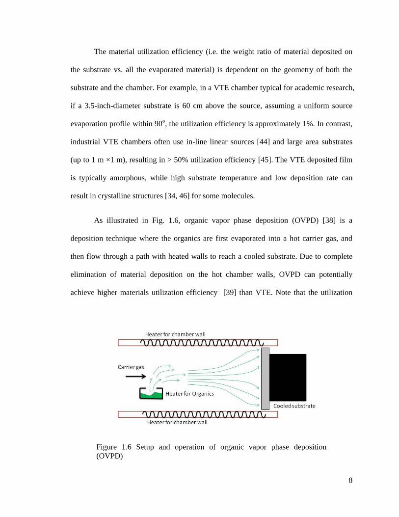
As illustrated in Fig. 1.6, organic vapor phase deposition (OVPD) [38] is a
deposition technique where the organics are first evaporated into a hot carrier gas, and
then flow through a path with heated walls to reach a cooled substrate. Due to complete
elimination of material deposition on the hot chamber walls, OVPD can potentially
achieve higher materials utilization efficiency [39] than VTE. Note that the utilization
Figure 1.6 Setup and operation of organic vapor phase deposition
(OVPD)

9
efficiency of OVPD also significantly depends on source and substrate geometry. In
addition, a variety of crystalline film morphologies can be achieved through tuning the
source temperature, carrier gas flow rate, chamber pressure and substrate temperature [29,
39].
Organic vapor jet printing (OVJP) [40] is a deposition technique based on the
same principles as OVPD, where the principal difference is that the organic vapor reaches
the cooled substrate surface through a heated nozzle. In contrast to the use of shadow
masks in VTE for organic film patterning, OVJP growth can be directly patterned on the
substrate with <10 µm resolution [41]. At the same time, OVJP offers superior material
utilization efficiency because the deposition occurs in the near field with < 1 mm
substrate-to-nozzle distance, and also there is no material loss due to shadow masks.
Although industrial fabrication of organic devices (i.e. OLED displays and light panels)
is presently solely through VTE, OVPD and OVJP have the potential to replace VTE in
the near future.
1.3 Organic Light Emitting Diodes
Research on OLEDs can be dated back to half a century ago when
electroluminescence from organic crystals was first observed. Most notably, in 1963,
Pope et al. [47] observed light emission from 10-micron-thick tetracene doped anthracene
crystals when the applied voltage was higher than 400 V, corresponding to 100 µA/cm2
current density. During the 1970s and 1980s [37, 48-50], organic electroluminescence
research gradually shifted from single crystals to polycrystalline and amorphous films. In
particular, in 1987, the work of Tang and VanSlyke [37] on a bi-layer Alq3 and 1-bis[4-

10
[N,N-di(4-tolyl)amino]phenyl]-cyclohexane (TAPC) device grown on an indium-tin-
oxide (ITO) coated glass substrate marked the birth of modern OLED technology. The
concept of the electron transport layer (ETL) and hole transport layer (HTL) in the Tang
device is still used in state-of-the-art OLEDs today. The next giant leap in OLED
technology happened in the late 1990s, when phosphorescent OLEDs were demonstrated
by the groups led by Forrest and Thompson [51, 52], which led to OLEDs with ~100%
internal quantum efficiency (IQE) [53].
Figure 1.7 illustrates the basic structure and operation of an OLED. Typically, a
bottom emitting OLED is grown on transparent substrates such as glass or plastic, with
an ITO anode, and an aluminum cathode on top. The organic layers sandwiched between
the electrodes typically have a total thickness of 100-200 nm. During operation (i.e. when
current is turned on), holes are injected from ITO and transported through the HTL to
Figure 1.7 Structure and operation of an organic light emitting diode
(OLED) consisting of an anode, a hole transport layer (HTL), a emissive
layer (EML), an electron transport layer (ETL), and a cathode. The
arrows show representative organic molecules used for different layers.
The processes of 1-5 are electron injection, hole injection, electron
transport, hole transport, and electron-hole recombination, respectively.

11
reach the emissive layer (EML); electrons are injected from aluminum and transported
through the ETL to reach the EML. When an electron and a hole reach each other inside
the EML, they combine to form a bound excited state called exciton. OLED emission
results from radiative decay of the excitons.
Depending on the total spin quantum number of the exciton, it is either a triplet
(spin number = 1) or a singlet (spin number = 0), and the formation ratio of singlets vs.
triplets was shown to be 1 vs. 3 [54, 55], following the spin degeneracy statistics. OLEDs
utilizing singlets for emission are called fluorescent OLEDs, in which triplet transitions
are spin forbidden and hence non-emissive. Therefore, the maximum internal quantum
efficiency, IQE (i.e. the ratio of the number of the input electrons and the generated
photons) of fluorescent OLEDs is only 25%. Recently, it was discovered that by utilizing
Figure 1.8 (a) A prototype flexible phone from LG, (b) A tablet
computer from Samsung, (c) A smart watch from Samsung, (d) A TV
from LG. All these electronic devices use OLED displays.

12
triplet-triplet annihilation, the theoretical limit of fluorescent OLED IQE can, in principal,
be increased to 62.5% [36, 56, 57], which will be discussed in detail in Chapter 6.
OLEDs utilizing triplets for emission are called phosphorescent OLEDs in which singlets
undergo rapid intersystem crossing to form triplets; thus, the theoretical maximum IQE of
phosphorescent OLEDs is 100% [51-53]. After the demonstration of phosphorescent
OLEDs, it was shown that phosphorescence-sensitized fluorescent OLEDs could also
reach 100% IQE [58, 59].
OLEDs are by far the most widely used organic electronic devices, and the main
applications are divided into displays and lighting. It is worth noting that all commercial
OLEDs are based on small molecules rather than polymers due to their superior
efficiency and operational stability.
As shown in Figure 1.8, OLED displays have been adopted in mobile phones,
electronic tablets, watches, cameras, computer monitors, TV screens, etc. According to
DisplaySearch (http://www.displaysearch.com/), the global market of OLED displays
was $8 billion in 2013, with mobile displays making up well more than half of the
revenue. The most well-known OLED displays are the ones used in Galaxy smart phones
made by Samsung. The advantages of OLED displays over conventional liquid crystal
displays (LCDs) include light weight, high contrast ratio, fast response, large color gamut
[60] (especially for the green sub-pixel), high mechanical flexibility, and low power
consumption. However, the drawbacks for OLED displays compared to LCDs include
high fabrication cost and limited operational lifetime. The lifetime issue for OLEDs is
most significant for blue phosphorescent emission (among red, green and blue sub-pixels
for displays), and in Chapter 8, we will show that significant improvement in blue

13
phosphorescent OLEDs lifetime can be achieved by a combined material and device
architecture approach.
Compared to OLED displays, OLED lighting is still gaining momentum to be
fully commercialized. In comparison to its strong competitor, LED lighting, OLED
illumination has the advantage of mechanical flexibility, low heat generation, and color
tunability. Although the high cost of the OLED light panel is the main hurdle for its wide
application, the fabrication cost can significantly decrease with the increase of
manufacturing scale. Both OLED and LED lighting panels have superior power
efficiency [61], environmental impact (i.e. material toxicity), operational lifetime, as well
as color purity when compared to conventional incandescent or fluorescent lighting.
One interesting but undesired feature of OLED operation is that its efficiency
decreases as the output luminance increases, often called efficiency roll-off. Although
inorganic LEDs also suffer efficiency roll-off [62], the on-set current density for roll-off
is much higher (> 10 A/cm2) for inorganic LEDs than for OLEDs (~ 0.1 A/cm
2). Note
that the OLED efficiency roll-off can be compensated by a large emissive area, which is
difficult to achieve using inorganic LEDs. A significant portion of this thesis (i.e.
Chapters 3, 4, 6, and 7) is devoted to understanding the physics related to such a
phenomenon and pursuing solutions.
1.4 Organic Semiconductor Lasers
Similar to OLEDs, research on organic semiconductor lasers (OSLs) has a long
history. The first demonstration of an optically pumped organic liquid dye laser was by

14
Sorokin et al. at IBM Watson Research Center in 1966 in chloro-aluminum pthalocyanine
(ClAlPc), only 6 years after the first demonstration of the ruby crystal laser. Liquid dye
lasers have the advantage of wavelength tunability, low cost, self-repairable (due to liquid
circulation), and the capability of achieving ultrafast pulses (<10 fs). However, the
disadvantages are the operational lifetime of dyes (which require frequent change of dye
and solution), and their toxicity.
Significant breakthroughs in organic thin film lasers occurred in the 1990s, when
amplified spontaneous emissions (ASE) were demonstrated by Heeger’s group and
Friend’s group using poly-phenylenevinylene (PPV) [63, 64], and unequivocal lasing was
reported by Forrest’s group using Alq3 doped with 4-(dicyanomethylene)-2-methyl-6-(4-
dimethylaminostyryl)-4H-pyran (DCM) [65]. Because these materials systems are
organic semiconductors, these organic lasers are also called organic semiconductor lasers
(OSLs) [66]. In all cases, they required an optical pump. In the late 1990s and early
2000s, organic thin film laser researchers were encouraged by the rapid development of
OLEDs, and it was envisioned that an electrically pumped OSL would soon be
demonstrated [67, 68]. Unfortunately, it has not yet been demonstrated to date. In
Figure 1.9 Chemical structures of organic semiconductor laser materials:
(a) Alq3, (b) 4-(dicyanomethylene)-2-methyl-6-julolidyl-9-enyl-4H-
pyran (DCM2), and (c) poly[9,9-dioctylfluorene-co-9,9-di(4-methoxy-
phenyl)fluorene] (F8DP)

15
Chapters 5 and 9, we will discuss the difficulties in achieving an electrically pumped
OSL, and our effort towards its demonstration.
Two essential components of any laser are the gain medium and the feedback
structure. In Fig. 1.9, we show common organic semiconductor lasing materials. Alq3
(Fig. 1.9 (a)) doped 4-(dicyanomethylene)-2-methyl-6-julolidyl-9-enyl-4H-pyran (DCM2,
Fig. 1.9 (b)) were among the earliest demonstrated OSL systems [10]. Figure 1.9 (c)
shows poly[9,9-dioctylfluorene-co-9,9-di(4-methoxy-phenyl)fluorene] (F8DP) [13],
which holds the lowest reported threshold record among all OSLs of 36 nJ/cm2. The
optical gain from OSL materials originates from the population inversion in a four-level
system made arising from the vibronic levels in the singlet excited state and the ground
state. The physics leading to laser action will be discussed in Chapter 2.
Figure 1.10 shows common feedback structures for OSLs. The planar waveguide
structure (Fig. 1.10 (a)) depends on reflections from the organic film and air interface to
Figure 1.10 Three different feedback structures for OSLs: (a) planar
waveguide, (b) vertical cavity, and (c) distributed feedback. The black
arrows show feedback directions and the red arrows show lasing (i.e.
out-coupling) direction.

16
provide feedback, leading to an edge emitting device. It typically has a high lasing
quantum efficiency (>70% was demonstrated by the Forrest group [65]) due to its
multimode nature. The vertical cavity structure (Fig. 1.10 (b)) depends on the top and
bottom mirrors (using silver or dielectrics) for feedback, and is thus surface emitting. The
feedback mechanism in a distributed feedback (DFB) structure (Fig. 1.10 (c)) is
diffraction from an integrated grating, which can be conveniently fabricated through
interference lithography [69] (see Chapter 5). Depending on the diffraction order, the
emission from DFB lasers can be either from the surface or from the edge.
Conventional optically pumped OSLs require a pump pulse shorter than 20 ns,
which is caused by the temporal increase of losses associated with the non-emissive
triplet excitons. Giebink et al. [4] and Lehnhardt et al. [70] studied the transient
intensities of OSLs pumped by long pulses (>100 ns), and found that both triplet
absorption and interactions between singlets and triplets limits the OSL operation to only
the nanosecond pulsed mode. In Chapter 5 we will show that such triplet induced losses
can be suppressed through the mixing of “triplet manager” [71] molecules into the gain
medium. Furthermore, we theoretically demonstrate that a continuous-wave operation
regime exists for OSLs, which is supported by the transient emission data from OSLs
using “triplet managers”.

17
1.5 Organic Solar Cells
At approximately the same time when Tang et al. published the first OLED
structure with respectable efficiency (i.e. approximately 1% EQE), another work from
Tang reported an organic thin film solar cell with 1% power conversion efficiency (PCE,
defined as the ratio of the maximum generated electrical power to the incident solar
power) [72]. The reported solar cell employed a bi-layer donor-acceptor type of
heterojunction, where excitons split into electrons and holes at the bi-layer interface, thus
generating current. After nearly 30 years of research, still using the same donor-acceptor
concept, PCEs close to or higher than 11% have been achieved in organic solar cells
(OSCs) using either small molecules or polymers [73, 74].
As illustrated in Fig. 1.11, the basic structure [72] of a planar OSC includes an
ITO anode, an electron donor layer, an electron acceptor layer, and a cathode. The
Figure 1.11 Structure and operation of an organic solar cell (OSC) made
of donor and acceptor bi-layer organics, the arrows show representative
organic molecules used for donors and acceptors. The processes of 1-5
are photon absorption (or exciton formation), exciton diffusion, exciton
splitting, hole diffusion, and electron diffusion, respectively.

18
operation of OSCs can be regarded as the inverse process of OLED operation. Sunlight
incident from the transparent ITO side is absorbed by the donor and acceptor layers.
Excitons are formed following absorption, which diffuse to the donor-acceptor interface
and split into electrons and holes that are subsequently collected at the electrodes.
For the same reason (i.e. high structural disorder) as low charge mobility
mentioned in Section 1.1, the exciton diffusion length in organics is also low, leading to
loss of excitons in planar OSCs. Use of bulk and nanocrystalline mixed heterojunctions
(i.e. comprised of a mixed donor and acceptor layer) [75, 76] moves the exciton splitting
interface closer to the exciton generation site, and thereby eliminates the need for long
diffusion. This has been shown effective in yielding higher PCEs.
Wide commercialization of OSCs is still challenging due to their low efficiency,
short operational lifetime, and high cost compared to inorganic solar cells. However, the
unique features of OSCs such as their mechanical flexibility and optical transparency can
potentially push OSCs to the market and fill roles that inorganic solar cells cannot
accomplish. For example, Fig. 1.12 shows curved organic solar panels installed in bus
Figure 1.12 Curved OSCs installed on the bus shelters in San Francisco.

19
shelters in San Francisco.
1.6 Organic Thin Film Transistors
The first organic thin film transistor (OTFT) was demonstrated by Tsumura et al.
[77] in 1986 using a polythiophene thin film with a carrier mobility of 10-5
cm2V
-1s
-1 and
a current on-off ratio of less than three orders of magnitudes. Through use of crystalline
organic thin films, the performance of OTFTs can surpass that of amorphous silicon, with
the calculated carrier mobility as high as 10 cm2V
-1s
-1 (note that these high mobilities are
likely due to charge transport on organic surface and can differ significantly from organic
bulk mobilities) [28, 78] and the current on-off ratio larger than 108 [79].
The basic structure of an OTFT and the representative organic molecules used are
shown in Fig. 1.13. The current-voltage relationship between the drain and source
electrodes (IDS-VDS) of an OTFT can be modulated by the voltage applied through the
gate and source electrodes (VGS). As illustrated in Fig. 1.14 (left), the IDS-VDS
Figure 1.13 Basic structure of an organic thin film transistor (OTFT),
and common organic molecules used in OTFTs, pentacene, rubrene, and
alpha-sixithiophene (α-6T).

20
characteristics of a transistor are typically divided into a linear region and a saturation
region. The linear region (when VDS < VGS) is a result of Ohm’s law, and the saturation
region (when VDS ≈ VGS) happens when the electric field near the drain electrode vanishes
and the accumulation region width approaches zero [1]. Transistors typically operate in
the saturation region when IDS is solely modulated by VGS.
Compared to inorganic thin film transistors, OTFTs have advantages in terms of
cost and mechanical flexibility; however, the reliability [80] and carrier mobility in
OTFTs still need improvement in order to compete with inorganic transistors.
Applications of OTFTs include the backplanes for flexible and/or transparent OLED
displays, radio frequency identification tags (RFID), chemical sensors, etc. Another
interesting application of OTFTs is to make electronic paper (Fig. 1.14 (right)) [81],
where the switch of OTFTs controls the status of electronic ink capsules, and thus the
color of the pixels.
Figure 1.14 (left) Drain-source current-voltage characteristics (IDS-VDS)
modulated by the gate-source voltage (VGS) (right) An electronic paper
prototype by SONY.

21
Chapter 2
Physics of Organic Semiconductors
Following the introduction to the general features of organic semiconductors,
their processing techniques, and applications in Chapter 1, we discuss in this chapter the
physics of organic semiconductors. This chapter is divided into three sections. In Section
2.1, we discuss the electrical properties of organic semiconductors, covering the
processes of charge injection, transport, and recombination. In Section 2.2, we focus on
the photophysics of organic materials, covering the concepts of excitons, exciton transfer,
and exciton interactions. In Section 2.3, the influence of exciton interactions on OLED
efficiency is discussed.
2.1 Electrical Properties of Organic Semiconductors
2.1.1 Charge Injection
The electron and hole transport states in organic semiconductors are called the
LUMO (lowest unoccupied molecular orbital) and HOMO (highest occupied molecular
orbital) respectively. The absolute values of the orbital energies are referenced to the
vacuum energy level. Ultraviolet photoelectron spectroscopy (UPS) and inverse
photoelectron spectroscopy (IPES) [82, 83] can be used to measure the HOMO ( HOMOE )

22
and LUMO ( LUMOE ) energies respectively. Molecular orbital energy levels are
conceptually comparable to the conduction and valence band extrema in inorganic
semiconductors; however, it is worth noting that intrinsic organic semiconductors have a
very low free carrier concentration (< 105 cm
-3) due to the large bandgap (ELUMO-EHOMO >
2 eV). Moreover, due to film morphology, disorder and interactions between charges and
their local environments (for example, phonons or molecular dipoles), molecular orbitals
are highly localized [84].
Charge injection in organics is the process of charge moving from the Fermi
surface of the metal electrodes to the frontier molecular orbitals of an organic
semiconductor. As shown in Fig. 2.1 (a), an electron injected from the metal Fermi level,
FE into the organic LUMO level, LUMOE , needs to overcome a built-in barrier height of
LUMO FV E E . The earliest physical model for such type of injection is thermionic
emission described by Richardson [85]:
Figure 2.1 (a) Illustration of the barrier height for current injection from
metal contact to organics (b) Barrier height reduction due to the
interfacial electric field

23
J =
eme
2p 2 3(k
BT )2 exp -
DV
kBT
é
ëê
ù
ûú
,
(2.1)
where J is the current density, e is the electron charge, em is the electron mass, Bk is
the Boltzmann constant, is the reduced Planck’s constant, and T is the temperature.
The Richardson model was later improved by Schottky [86] to include the effect
of barrier height reduction, , due to the interface electric field (Fig. 2.1 (b)). Emtage et
al. [87] further derived expressions relevant to insulators (or organic semiconductors)
with low charge mobility, which simplifies to the following equations under the limit of
low electric field and high electric field respectively:
exp( )low e
B
VJ N eF
k T
(2.2)
1/4
34 expBhigh e
B
k T VJ N eF
k T
(2.3)
where eN is the electron density of states, is the mobility, F is the electric field at
the metal/insulator interface, and is the dielectric constant of the insulator.
More recent improvements of the thermionic emission model relevant to the
injection into organics was from Scott and Malliaras [88], which included an organic-to-
metal interface reverse recombination current in addition to the metal-to-organic injection
current. This model was later used to understand charge injection in OLEDs [89, 90].
Besides thermionic emission, another method for modeling current injection in
organics is by Fowler and Nordheim [91] of electron tunneling through the injection

24
barrier. Fowler-Nordheim tunneling results directly from solving Schrödinger’s equation
for a triangular barrier,
3/2
24 2
exp3
FN
m VJ BE
eF
(2.4)
where B is a tunneling pre-factor. This model was also successfully applied to modeling
charge injection OLEDs [92, 93]; however, the barrier reduction effect due to the
interface electric field is not considered by Eq. (2.4), which could cause significant
overestimate of the tunneling efficiency.
The drawback for applying the thermionic emission or tunneling model is that
neither considers the energetic disorder in organic semiconductors. To include such
disorder in organics, Arkhipov et al. [94] and Baldo et al. [95] considered the Gaussian
distribution of the molecular orbital energies, and the Miller-Abraham type [96] hopping
between the metal and organic interface,
0
0
exp 0( )
0
B
VA V
R V k T
A V
(2.5)
where R is the hopping probability between sites with an energy barrier of V , and 0A
is the maximum hopping rate determined by the molecular orbital overlap. Then, the total
injection current density is the integral over all possible states,
22
1 1( )exp
2 2
( )
OII O I
I O
O I
UUJ dU dU f U
R U U aeF
(2.6)

25
where IU and OU are the disorder energies of the metal-organic interface states, and the
organic bulk respectively, I and O are the standard deviations of the Gaussian energy
distributions, f is the distribution of the interface states, and a is the average
intermolecular spacing. By modeling the J-V characteristics in a broad selection of
organic semiconductors and temperature range using Eq. (2.6), Baldo et al. [95]
suggested that the current density in organics is often limited by interface injection rather
than organic bulk transport. However, mechanisms determining the J-V characteristics in
organics are still under intense research investigation.
2.1.2 Charge Transport
When a molecule in organics is charged, due to both electron-phonon coupling
and the polarization of the surrounding molecules by the charge, its configuration is
distorted and energy is relaxed to a lower level than its molecular orbital energy [47].
This newly formed quasi-particle is called a polaron, and charge transport in organics is
through polaron hopping between discrete molecular sites.
The earliest model for charge transport in organics was the space charge limited
current (SCLC) model introduced by Mott and Gurney [97], and Rose [98], which
assumed the charge injection from electrodes into organics is efficient (i.e. the contact is
Ohmic). The derivation of the SCLC J-V relation starts from the Ohm’s law and Gauss’s
law,
J ep F (2.7)

26
0r
dF ep
dx (2.8)
where p is the hole density (and the same expression applies to the electron density n),
r is the relative permittivity of the insulator, and 0 is the vacuum permittivity.
Integrating Eq. (2.7) after plugging in Eq. (2.8) yields,
0 0
2
r r
J xJdx FdF F
. (2.9)
Then, integrating one more time yields the quadratic Mott-Gurney J-V relationship,
20
3
0
2 9
8
rSCLC
r
xJFdx dx J V
d
. (2.10)
If there are trap states within the bandgap of the organics which have an
exponential distribution in energy, ( )TN E relative to the molecular orbital energies (for
example, LUMO),
( ) expLUMO LUMOT
B T B T
N E EN E
k T k T
(2.11)
where LUMON is the trap density at the LUMO energy, TT is a trap distribution
temperature, Rose also derived the following expression for trapped charge limited
current (TCLC).

27
1 1
0
2 1 2 1
2 1
1
l l l
rTCLC C l l
LUMO
ll VJ q N
qN dl
(2.12)
where CN is the density of states at the LUMO energy, and /Tl T T . Equation (2.12)
was applied to a large selection of organic materials [99-103], with the factor l typically
in the range of 6-10.
Interestingly, it was pointed out by Lampert [104] that the J-V characteristic of
insulators with Ohmic contacts is confined to a triangular area illustrated in Fig. 2.2
(when both the J and V axes are in a log scale) defined by three limiting curves: Ohm’s
law, SCLC, and TCLC. This theory has been routinely and successfully applied to
organic semiconductors [105, 106].
Figure 2.2 The current density-voltage (J-V) triangle (shaded) formed by
three charge transport mechanisms in organics: Ohm’s law, space charge
limited current (SCLC), and trapped charge limited current (TCLC)
28
2.1.3 Charge Recombination
Charge recombination occurs when the electrons and holes coexist in the same
spatial location but at their respective energies. The recombination rate, R, in organics is
generally modeled following the treatment of Langevin assuming that electrons and holes
move towards each other under the influence of their mutual Coulomb interaction,
0
( )n p
L
r
eR np k np
(2.13)
where n and p are electron and hole mobilities, respectively, and Lk is the Langevin
recombination rate. Following recombination, the electron and hole form a bound excited
state, or exciton, which plays a central role in the photophysical properties of organic
semiconductors.
2.2 Photophysical Properties of Organic Semiconductors
2.2.1 Excitons: Types and Definitions
When organic molecules are excited, an electron from the HOMO is promoted to
the LUMO, leaving a hole in the HOMO, and the resulting electron-hole pair is bound
through Coulomb interaction to form an exciton.
As shown in Fig. 2.3, depending on the spatial extent of excitons, they can be
divided in three different types [107, 108]: Frenkel excitons, charger transfer excitons,
and Wannier-Mott excitons. The most common excitons in amorphous semiconductors
are of the Frenkel type, which has the most localized (usually confined to a single

29
molecule) wave function and the highest binding energy BE (~ 1 eV) among the three.
Charge transfer excitons have a broader spatial extent than Frenkel excitons, and are
often reported in organics with local crystalline order [47]. Frenkel and charge transfer
excitons may also exist in the same organic material [109]. The delocalized Wannier-
Mott exciton has a small BE (< 10 meV), and is generally observed in high dielectric
constant crystalline inorganic semiconductors.
The energy of an exciton relative to the molecular ground state can be solved
through its Hamiltonian, Hex, which is the summation between the single excited electron
Hamiltonian He, and the electron-electron interaction, Uee,
ex e ee e e eeH H U T U U (2.14)
where Te and Ue are the single electron kinetic and potential energies, respectively. Under
the Born-Oppenheimer approximation [110], He can be calculated by solving the electron
energy in a stationary molecular nuclear configuration. The discrete eigen-energies of He
for the molecular ground and excited states in the configuration coordinate scheme [110]
are illustrated in Fig. 2.4. The energy spacings between the eigen-energies in the same
Figure 2.3 Three type of excitons determined by their spatial extent.

30
state are approximately the same due to the parabolic shape in Ue close to the energy
minimum.
The interaction in Eq. (2.14) is given by 0 12
1
4ee
eU
r , where 12r is spatial
separation between the excited electron in the LUMO and the unpaired electron left in the
HOMO. Then, the eigen-energies for eeU can be calculated through ee eeE U ,
where is the spatial wave function of the two-electron system.
Depending on the symmetry of the spin wave functions, excitons can be either
spin anti-symmetric singlets or spin symmetric triplets. The total wave function of an
exciton is the product of the spin wave function and the spatial wave function. Since
electrons are Fermions whose total wave function is anti-symmetric, the singlet spatial
wave function S is symmetric and the triplet spatial wave function T is anti-
symmetric:
Figure 2.4 Ground state and excited state energies in the molecular
configuration coordinate. The numbers (0-3) are the indexes for different
vibronic states.

31
1(1) (2) (2) (1)
2
1(1) (2) (2) (1)
2
S HOMO LUMO HOMO LUMO
T HOMO LUMO HOMO LUMO
(2.15)
where HOMO and LUMO are the wave functions for the HOMO and LUMO respectively,
and 1 and 2 are indices for the two electrons. Thus, interaction energies for singlets (ES)
and triplets (ET) are
0 12
1
4S S S
eE J K
r
(2.16)
and 0 12
1
4T T T
eE J K
r
(2.17)
where J and K are the Coulomb and exchange energies, respectively:
2
0 12
1(1) (2) (1) (2)
4HOMO LUMO HOMO LUMO
eJ
r
(2.18)
2
0 12
1(1) (2) (2) (1)
4HOMO LUMO HOMO LUMO
eK
r
. (2.19)
Therefore, the molecular singlet energy is higher than triplet by 2K.
Optical transition (i.e. absorption and emission) rates in organics can then be
calculated through dipole transitions between a molecular ground state and excited state
using the Fermi’s Golden rule,

32
2
222
2( )
3
2| ( )
3
f f i i f
f i f i f
S H S E
F S S d E
(2.20)
where iS and fS are the spin wave functions of the initial and final states, i and f
are the spatial wave functions of the initial and final states, H = dF is the transition
Hamiltonian, where d is the dipole moment, and ( )fE is the density of the final state
with the energy fE . Clearly, the spin symmetries of the initial and final states need to be
the same for to be non-zero, which is called the dipole transition selection rule.
Because most molecules have a spin symmetric ground state due to the filled HOMOs,
only singlet excitons are responsible for absorption and emission in fluorescent organic
molecules. The absorption and emission processes in an archetype organic molecule
Figure 2.5 (left) Emission and absorption spectra of a prototype
fluorescent molecule, anthracene (the chemical structure is shown in the
inset) dissolved in cyclohexane, and the corresponding transitions (right)
between the singlet excited state and ground state. The energy of triplet
is lower than singlet by ΔEST= 2K (see Eq. (2.19)), and the triplet is non-
emissive.

33
anthracene are illustrated in Fig. 2.5, and the vibronic spectral peaks are explained by
transitions between discrete levels in the ground and singlet excited states.
Early demonstrations of OLEDs [37] were based on fluorescent emission from
singlets; however, electron-hole recombination in OLEDs forms both singlets and triplets
with a ratio of 1:3 [55] determined by the spin degeneracy. Since triplets are non-
emissive due to the dipole transition selection rule, the maximum internal quantum
efficiency (IQE) in fluorescent OLEDs is only 25%. Fortunately, the selection rule can be
broken by the strong spin-orbit coupling in phosphorescent molecules due to the mixing
of singlet and triple states, usually effected by insertion of a metal atom with high orbital
angular momentum into the molecule. The Hamiltonian, SOH for spin-orbit interaction is
[110],
2
2 2 3
08SO
e
ZeH l s
m c r (2.21)
where Ze is the charge of the nucleus, me is the electron mass, c is the speed of light, r is
the electron-nucleus distance, l and s are the electron orbital and spin angular
momentum, respectively. To see how HSO mixes singlets and triplets, apply
1, 1, 2, 2,1 2
1, 2, 1, 2, 1, 2, 1, 2,1 2 1 2
( )
( ) ( ) ( ) ( )
z z z zSO z
z z z z z z z z
H A l s A l s
A l A l s s A l A l s s
(2.22)
to 1,0 0,0SO zH . Since, 1, 2, 1, 2,1 21,0 ( ) ( ) 0,0 0z z z zA l A l s s ,

34
1, 2, 1, 2,1 2
1, 2,1 2
1 1, 2 2,
11,0 0,0 1,0 ( ) ( ) 0,0
2
1,0 1,02
( )2
z z z zSO z
z z
z z
H A l A l s s
A l A l
Al A l
(2.23)
where 1,0 is a triplet with zero spin in the z direction, and 0,0 represents a singlet
wavefunction. From Eq. (2.23), it is evident that SOH breaks the transition rules between
singlets and triplets, thus allowing singlet-to-triplet intersystem crossing as well as triplet
emission.
Since r3 is proportional to 1/Z
3, Eq. (2.21) implies that HSO is then proportional to
Z4. Thus, the spin-orbit coupling effect is significantly stronger for a nucleus with a large
atomic number. This concept guided the early discovery of efficient triplet emitters based
on heavy metal (such as iridium and platinum) complexes, and thus the demonstration of
Figure 2.6 Chemical structure and emission spectrum (when doped at 2
vol% in Alq3) of an archetype phosphorescent molecule, platinum-
octaethyl-phorphyrin (PtOEP).
35
efficient phosphorescent OLEDs (PHOLEDs) [51, 52]. Figure 2.6 shows the chemical
structure and emission spectrum of platinum-octaethyl-phorphyrin (PtOEP), based on
which the first PHOLED was demonstrated.
2.2.2 Exciton Transport
Exciton transport refers to both the individual exciton energy transfer and the
collective behavior of exciton diffusion. We first discuss the mechanisms for exciton
transfer, and then show how exciton diffusion relates to the individual transfers.
Exciton transfer occurs from a donor (D) to an acceptor molecule (A, which may
or may not be a different type from D). The rate of exciton transfer can also be calculated
by Eq. (2.20) using *
i D A and *
f D A , where the wave functions, D and A
represent the donor and acceptor ground states, and *
D and *
A are the donor and
acceptor excited states.
If the transfer Hamiltonian in Eq. (2.20) is a dipole-dipole interaction,
3 2
0
1 1 3( )( )
4AD ADD A D Adipole
AD AD
H d d d R d RR R
(2.24)
where RAD is the vector from the donor to the acceptor, d D and d A are the dipole
moments of the donor and acceptor, respectively. Förster [111] first solved this
Hamiltonian, deriving the Förster transfer rate, F given by:

36
6
1 FF
D AD
R
R
.
(2.25)
Here
1/64 4
4 4
3 1( ) ( )
4F D A
cR F E E dE
n E
(2.26)
is the Förster radius, D is the donor exciton lifetime, ( )DF E is the donor emission
spectrum normalized to the photoluminescence quantum yield PL by ( )D PLF E dE ,
and ( )A E is the acceptor absorption cross section.
Due to the dipole transition selection rule, Förster transfer between fluorescent
molecules is only allowed for singlets; however, Förster transfer of triplets from
phosphorescent molecules is allowed [58] for the same reason as triplet emission is
allowed – i.e. due to strong spin-orbit coupling (see Eq. (2.23)). The emissive layer of
fluorescent OLEDs typically utilizes the host-dopant architecture, where charge transport
and recombination are through the host, and excitons on the host subsequently Förster
transfer to the dopant for emission to occur. The Förster radius for such host-dopant
system with strong emission and absorption overlap is typically 3 - 5 nm [10].
Hamiltonians containing other than dipole-dipole interactions in Eq. (2.20) can
also give rise to exciton transfer. Most notably, Dexter [112] considered the electron-
electron exchange interaction, whose matrix element is:

37
* * * *
0 12
* * * *
0 12
1 1(2) (2) (1) (1) (1) (1) (2) (2)
4
1 1(2) (1) (1) (2) (2) | (2) (1) | (1)
4
exchange D D A A D D A A
r
D A D A D A A D
r
H S S S Sr
S S S Sr
(2.27)
where S and are the spin and spatial wave functions respectively. After calculating
Eq. (2.20) using Eq. (2.27), the Dexter transfer rate is:
22
( ) ( )D exchange D AH F E E dE
. (2.28)
Note that Dexter exciton transfer only requires separate spin conservation in the
two initial states and the two final states (a result of Eq. (2.27)); therefore, triplet transfer
in fluorescent molecules is allowed by the relatively short-range Dexter transfer.
The collective motions of incoherent exciton transfer results in exciton diffusion,
described by [113],
¶N (r,t)
¶t= G(r,t) -
N (r,t)
t+ DÑ2N (r,t) (2.29)
where N (r,t) is the exciton concentration, G(r,t) is the exciton generation rate, is
the exciton lifetime, and D is the exciton diffusivity. Assuming simple cubic lattice
exciton diffusion sites and diffusion through only nearest neighbors, D can be calculated
from the nearest neighbor exciton transfer rate nn through:
2
nnD a (2.30)

38
where a is the lattice constant. The exciton diffusion length DL D is then defined by
the average diffusion distance of an ensemble of excitons within their lifetime.
2.2.3 Exciton Interactions
Exciton interactions that result in annihilation are a special type of exciton
transfer, where energy is transferred from an exciton to another excited state (exciton or
polaron). The transfer Hamiltonian, and thus the rate for exciton interaction, can be
calculated from Fermi’s Golden rule (Eq. (2.20)). Common exciton interactions [47, 114,
115] in organics include singlet-polaron annihilation (SPA) [115], triplet-polaron
annihilation (TPA) [116, 117], singlet-triplet annihilation (STA) [4, 118], triplet-triplet
annihilation (TTA) [116, 119], etc.
When annihilation involves a singlet, its energy transfer is typically dominated by
Förster type interactions (Eq. (2.25) and (2.26)), because the long-range dipole-dipole
interaction has a significantly higher rate than the Dexter type interaction (Eq. (2.27) and
(2.28)). In contrast, triplet annihilation usually follows Dexter type interactions.
The exciton annihilation rate depends on the relative distance between the energy
donor and acceptor, which is constantly changing as a result of exciton diffusion.
Therefore, as illustrated in Fig. 2.7, the description of collective exciton annihilation
should also involve exciton diffusion. For example, one type of TTA occurs through,
0 0
nT T T S T S (2.31)
where T is a triplet, nT is a hot triplet (i.e. a spin symmetric exciton with a higher
energy than T ), and 0S is the molecular ground state. Singlet formation during TTA is

39
neglected by Eq. (2.31), and is treated by Eq. (2.41) in the next section. Thus, a
description of triplet dynamics T r,t( ) considering both triplet diffusion and annihilation
is:
1
2 31 1 1
, 1, , , ,T TT
rT
T r tD T r t T r t U r r T r t dr T r t
t
(2.32)
where TD is the triplet diffusivity, T is the triplet lifetime, and TTU r is the interaction
rate between two triplets. Although an analytical solution does not exist for Eq. (2.32),
under the assumption that Eq. (2.31) occurs when two triplets are within a capture radius
RC following Smoluchowski [113], Eq. (2.31) can be simplified to,
¶T (r,t)
¶t= D
TÑ2T (r,t) (2.33)
Figure 2.7 Annihilation between excitons (red filled circles)
considering both exciton diffusion (dashed arrows) and exciton-
to-exciton energy transfer (solid arrow). The open circles are the
available transport site for excitons.

40
with the boundary condition , 0Cr R
T r t
.
Now, Eq. (2.33) can be solved in spherical coordinates with 0, 0T r t T :
( )
220
0
2, 1 exp
C
T
r R
C C D tR R
T r t T x dxr r
. (2.34)
Then, the triplet flux at the boundary Cr R in the frame of motion of a center triplet as
the annihilation center is:
2
0 04 4 1 4
C
CC T T C T C
r R T
RTR D D R T D R T
r D t
. (2.35)
After considering 0T of such triplets all acting as annihilation centers:
2 20
0 02 4 8
C
C T T C
r R
dT TR D T D R T
dt r
(2.36)
where the factor of 2 comes from the doubled diffusivity as a result of the relative motion
of the participating triplets. Thus, when using a simple TTA rate, 8TT T Ck D R , triplet
density dynamics considering both the triplet natural decay and TTA is then:
21
2TT
dT Tk T
dt . (2.37)
Similarly, exciton density decay due to bimolecular annihilation is generally
calculated by the product of the densities of the energy donors and acceptors, and an
annihilation rate.

41
2.3 Exciton Interactions in Organic Light Emitting Diodes
Exciton interactions result in a non-linear dependence of exciton density on
current density (J), thus contributing to change of OLED external quantum efficiency
(EQE) vs. J. The functions of J-V (as discussed in section 2.1) and EQE-J are the two
most important characteristics of an OLED. To model EQE-J in a fluorescent OLED, we
consider the following exciton interactions,
Singlet-triplet annihilation (STA) 0 0
nS T T S T S (2.38)
Singlet-polaron annihilation (SPA) 0 0
nS p p S p S (2.39)
Singlet-singlet annihilation (SSA) 0 0
nS S S S S S (2.40)
Triplet-triplet annihilation (TTA-S) 0 0
nT T S S S S (2.41)
Triplet-triplet annihilation (TTA-T) 0 0
nT T T S T S (2.42)
Triplet-polaron annihilation (TPA) 0 0
nT p p S p S (2.43)
where S , T , and p are the singlet, triplet, and polaron, and nS ,
nT , and np are the
intermediate hot singlet, triplet, and polaron (i.e. S , T , and p are excited to higher
energy states). The bimolecular interaction rates for Eq. (2.38) – (2.43) are kST, kSp, kSS,
kTT-S, kTT-T, and kTp, respectively. Assuming a uniform exciton formation rate in the OLED
active region of thickness d, the singlet and triplet density dynamics are,
2 21
4S SS ST Sp TT S
dS Jk S k S k ST k Sp k T
dt ed (2.44)

42
2 232
4T TT S TT T Tp
dT Jk T k T k T k Tp
dt ed (2.45)
where the factors of ¼ and ¾ in the generation terms are determined by the formation
ratio of singlet and triplet during charge recombination. If we only consider exciton
natural decay and STA, and neglect all other interactions, under equilibrium condition,
( )4 3
T
T S ST
JkS t
edk k k J
. (2.46)
Then, we can determine the EQE(J) in the fluorescent OLED as,
( )
( )/ 4 3
S S Tout PL out PL
T S ST
k S t d k k edEQE J
J e edk k k J
(2.47)
where out is the optical out-coupling efficiency, and PL is the radiative efficiency of the
emitter. From (2.47), it is evident that EQE(J) is a decreasing function of J, meaning that
the OLED is less efficient if operated at high J (or high luminance).
Similarly, assuming efficient inter-system crossing and only TTA (Eq. (2.42)) in a
phosphorescent OLED, the triplet density dynamics are determined by,
2
T TT T
dT Jk T k T
dt ed . (2.48)
Then, the EQE(J) in the phosphorescent OLED is
2 4
( )2
T TT Tout PL T
TT T
edk k JEQE J k
Jk ed
(2.49)
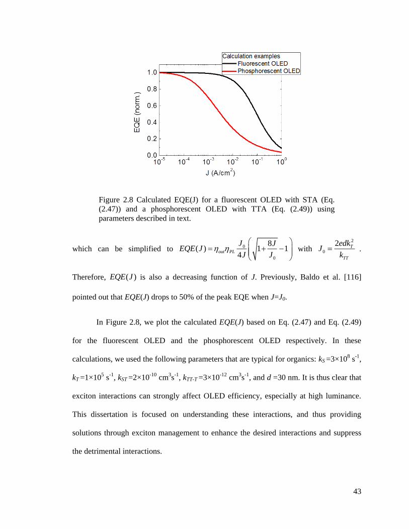
43
which can be simplified to 0
0
8( ) 1 1
4out PL
J JEQE J
J J
with
2
0
2 T
TT
edkJ
k .
Therefore, ( )EQE J is also a decreasing function of J. Previously, Baldo et al. [116]
pointed out that EQE(J) drops to 50% of the peak EQE when J=J0.
In Figure 2.8, we plot the calculated EQE(J) based on Eq. (2.47) and Eq. (2.49)
for the fluorescent OLED and the phosphorescent OLED respectively. In these
calculations, we used the following parameters that are typical for organics: kS =3×10⁸ s
-1,
kT =1×10⁵ s
-1, kST =2×10
-10 cm
3s
-1, kTT-T =3×10
-12 cm
3s
-1, and d =30 nm. It is thus clear that
exciton interactions can strongly affect OLED efficiency, especially at high luminance.
This dissertation is focused on understanding these interactions, and thus providing
solutions through exciton management to enhance the desired interactions and suppress
the detrimental interactions.
Figure 2.8 Calculated EQE(J) for a fluorescent OLED with STA (Eq.
(2.47)) and a phosphorescent OLED with TTA (Eq. (2.49)) using
parameters described in text.
44
Chapter 3
Singlet-Triplet Annihilation in
Fluorescent Organic Light Emitting Diodes
Electron-hole recombination (Eq. (2.13)) in OLEDs generates both singlets and
triplets. As discussed in section 2.2.3, once a singlet collides with a triplet, the triplet can
be temporarily excited to a hot triplet state, and then rapidly relaxed to its original triplet
state. This is a process known as singlet-triplet annihilation (STA), in which the singlet
energy is non-radiatively dissipated. Since singlets are responsible for fluorescent
emission, STA leads to a loss of fluorescent OLED efficiency. In this Chapter, we
introduce the dynamics of STA in fluorescent OLEDs, and then apply the dynamics to
explain electroluminescence (EL) transient turn-on decays in two prototype fluorescent
OLEDs. Finally, we discuss a strategy of de-exciting the detrimental triplets through the
use of a phosphorescent dopant which results in decreased STA and thus can potentially
improve fluorescent OLED efficiencies.
3.1 Dynamics of Singlet-triplet Annihilation (STA)
Figure 3.1 shows the basic structure of a bottom emitting OLED on glass
substrate. The organic layers consist of an emissive layer (EML) sandwiched between an

45
electron transport layer (ETL) and a hole transport layer (HTL). Electrons and holes
injected from the electrodes recombine in the EML, and the OLED emission is the out-
coupled light from singlet radiative decay. In this section, we model the singlet and triplet
dynamics after the charge recombination. It is shown that STA leads to singlet density
transient decays following the fluorescent OLED turn-on.
Triplet density dynamics in fluorescent OLEDs are determined by the processes
of triplet non-radiative decay, triplet-triplet annihilation (TTA), and triplet polaron
annihilation (TPA). Of these, TTA occurs through two routes [115],
0T T S S , (3.1)
and 0T T T S , (3.2)
where T is triplet, S is singlet, and 0S is the ground state. Considering spin statistics,
when two triplets annihilate, the result is the fractional production of 3/4 triplet excited
Figure 3.1 Structure of a bottom emitting OLED on glass substrate

46
states, 1/4 singlet excited state, and 1 molecular ground state [114]. Also, TPA is
described by,
0T n S n , (3.3)
where n is the polaron [120]. The polaron density arises both from injected charge
determined by current density at time ,t, ( )J t , and interfacial charge due to the junction
capacitance [115]. Then, assuming Langevin recombination,
dn
dt
J (t)
ed n2 , (3.4)
where d is the width of the exciton formation region which is approximately equal to the
width of the EML, and Lk is the Langevin recombination rate [89] , given by:
0
L h e
r
ek
(3.5)
Here, 2.9r is the relative permittivity of the EML, 0 is the permittivity of free space,
and h and e are the mobilities of holes and electrons in the EML, respectively.
Equation (3.4) neglects the charge transit time from the electrodes to the EML. A
complete treatment of the charge injection and transit can be found in [89]; our
approximation allows for a simplified analytical treatment.
According to Eq. (3.1) to (3.5), the triplet density dynamics are given by:
2 23 5
4 4L T TT TP
dTk n k T k T k nT
dt , (3.6)
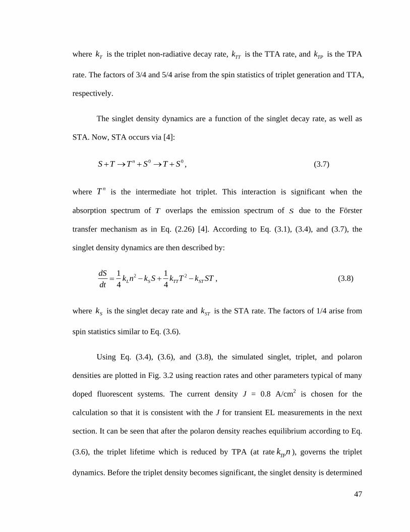
47
where Tk is the triplet non-radiative decay rate, TTk is the TTA rate, and TPk is the TPA
rate. The factors of 3/4 and 5/4 arise from the spin statistics of triplet generation and TTA,
respectively.
The singlet density dynamics are a function of the singlet decay rate, as well as
STA. Now, STA occurs via [4]:
0 0nS T T S T S , (3.7)
where nT is the intermediate hot triplet. This interaction is significant when the
absorption spectrum of T overlaps the emission spectrum of S due to the Förster
transfer mechanism as in Eq. (2.26) [4]. According to Eq. (3.1), (3.4), and (3.7), the
singlet density dynamics are then described by:
2 21 1
4 4L S TT ST
dSk n k S k T k ST
dt , (3.8)
where Sk is the singlet decay rate and STk is the STA rate. The factors of 1/4 arise from
spin statistics similar to Eq. (3.6).
Using Eq. (3.4), (3.6), and (3.8), the simulated singlet, triplet, and polaron
densities are plotted in Fig. 3.2 using reaction rates and other parameters typical of many
doped fluorescent systems. The current density J = 0.8 A/cm2 is chosen for the
calculation so that it is consistent with the J for transient EL measurements in the next
section. It can be seen that after the polaron density reaches equilibrium according to Eq.
(3.6), the triplet lifetime which is reduced by TPA (at rate k
TPn ), governs the triplet
dynamics. Before the triplet density becomes significant, the singlet density is determined

48
by the decay constant, Sk . As the triplet density increases over time, STA suppresses the
continued increase of the singlet density. This results in a peak in singlet density. As the
triplet density increases further, the STA term in Eq. (3.8) dominates, ultimately resulting
in a decrease in the singlet density. Since the light output in fluorescent OLEDs is
proportional to singlet density, STA leads to transient EL turn-on decays.
3.2 Transient Electroluminescence Turn-on Decay Due to STA
To observe the predicted EL transients, OLEDs were grown on commercially pre-
coated indium-tin-oxide (ITO) on glass substrates cleaned as described previously [121].
Organic layers are deposited in a vacuum thermal evaporation chamber with base
pressure < 5×10⁻⁷
Torr. A 40 nm thick 4,4’-bis[N-(1-naphthyl)-N-phenyl-amino]-
Figure 3.2 Simulated density dynamics according to the model in text for
a device at 0.8A/cm2 injection current density using the parameters
listed.

49
biphenyl (NPD) was first deposited as the hole transport layer (HTL), followed by a
25nm thick emission layer (EML), and a 30 nm thick bis(2-methyl-8-quinolinolate)-4-
(phenylphenolato)aluminum (BAlq) electron transport layer (ETL). The host, tris(8-
hydroxyquinoline) aluminum (Alq3), was doped with the red emitting fluorphore, 4-
dicyanmethylene-2-methyl-6-(p-dimethylaminostyryl)-4H-pyran (DCM), and 9,10-
Di(naphth-2-yl)anthracene (ADN) was doped with the blue emitting 2,5,8,11-tetra-tert-
butylperylene (TBP) for the OLED EMLs. The chemical structures of these molecules
are shown in Appendix A. The four OLEDs studied consist of the following dopant
concentrations: 3 vol% DCM:Alq3 (Device A1), 8 vol% DCM:Alq3 (A2), 3 vol%
TBP:ADN (B1), and 8 vol% TBP:ADN (B2). All devices were completed with a 0.8 nm
thick LiF layer followed by an 80 nm thick aluminum cathode deposited through a
shadow mask to form 1 mm2 square devices. The structures of the four OLEDs are
illustrated in Fig. 3.3.
Figure 3.3 Structures for red emitting OLEDs A1 and A2 (left), and blue
emitting OLEDs B1 and B2 (right). The short name of each layer is
explained in text and also in Appendix A.

50
After deposition, current-voltage-luminance (I-V-L) characteristics were measured
in atmosphere using an HP4155 parameter analyzer with a calibrated Si photodiode
following the standard procedures [122] (see Fig. 3.4 left). The OLED emission spectra
were measured using a fiber-coupled OceanOptics USB4000 spectrometer (see Fig. 3.4
right). The device was then loaded into a N2 chamber where the transient EL was
measured by excitation with rectangular current pulses at a repetition rate of 5Hz and
width of 100 µs from a HP8114A pulse generator. Emission was collected by a Si
avalanche photodiode (APD, Hamamatsu C5460), and monitored by an oscilloscope
(Tektronix 3054B).
Figure 3.5 shows the EL turn-on for devices A1 and B2 as functions of time and
current pulse amplitude. The ratio of peak-to-steady-state EL increases with drive current.
Also, the rise time (< 1 µs) is significantly shorter than the decay time (~ 20 µs). For
DCM:Alq3 devices (A1 and A2), the shape of the transient EL only weakly depends on
the dopant concentration, while for the TBP:ADN device (B1 and B2), the EL turn-on
Figure 3.4 (left) Setup for OLED density-voltage-luminance (J-V-L)
characterization. A parameter analyzer is used to measure the current
(IOLED) and voltage (VOLED) through the OLED, and the current (IPD)
through a calibrated photodetector. (right) Setup for OLED emission
spectrum measurement.

51
peak increases with doping concentration.
Fits to the data according to Eq. (3.4), (3.6), and (3.8) using the parameters in
Table 3.1 are indicated by solid lines. We note that the exciton formation region for the
four devices is located at the interface between the HTL and EML [123, 124]. Hence,
only the electron mobility is required in Eq. (3.5), which is extracted from the transient
EL turn-on delays in Fig. 3.5. Furthermore, triplet non-radiative decay and TTA in Eq.
(3.6) are neglected since these processes are negligible compared to TPA during the
device turn-on.
In the fits In Fig. 3.5, we assume that TPk and STk are independent of pulse
amplitude. The steady state current density range for the model fit is from 0.1 A/cm2 to
Figure 3.5 Transient electroluminescence (EL) of devices with 3% DCM:Alq3 (left,
device A1) and 8% TBP:ADN (right, device B2) in response to 100 µs current pulses of
different amplitudes. The steady state current density is indicated. Solid lines are the fits
to the STA model, which determine the STA rate of 1.9×10⁻¹⁰
cm3/s and 1.2×10
-10 cm
3/s
for A1 and B2, respectively. Similar fits are obtained for all four devices with results
summarized in Table 3.1.

52
1.0 A/cm2, over which the EL peaks are prominent. The predicted EL slightly deviates
from the experiment for the initial 1 µs due to our neglect of the charge transit time in Eq.
(3.4). From Table 3.1, the STA rates are unchanged for a given guest-host combination,
regardless of doping concentration. This is expected since STA is a Förster type
interaction (Eq. (2.26)) that only depends on the absorption spectrum of the triplet and the
emission spectrum of the singlet [4]. Note that our value for the DCM:Alq3 STA rate is in
agreement with values obtained from optical excitation (1.9×10⁻¹⁰
cm3/s) of this mixture
[4]. Furthermore, the ~ 50% decrease in the STA rate from 3% TBP:ADN to 8%
TBP:ADN results since TBP acts as a triplet or polaron trap, which decreases the triplet-
polaron collision probability as the TBP density decreases.
The turn-on peak recovery following the double pulse with varying delay times is
shown in Fig. 3.6 (a) for device B2. We observe that a > 600 µs delay is necessary for the
full recovery of the EL peak intensity. Fits of the data in Fig. 3.6 (a) to Eq. (3.4), (3.6),
and (3.8) provide the triplet density as a function of delay time shown in Fig. 3.6 (b). A
Table 3.1 Fitting parameters for transient ELs from the OLEDs
EML τS(ns) k
TP(cm
3/s) k
TS(cm
3/s) µ (cm
2/V/s)
3% DCM:Alq3 1.20.1 (5.60.4)×10-13
(1.90.2)×10-10
(1.20.2)×10-5
8% DCM:Alq3 1.10.1 (6.30.5)×10-13
(1.80.2)×10-10
(1.20.2)×10-5
3% TBP:ADN 2.30.1 (132)×10-13
(1.10.2)×10-10
(1.60.3)×10-5
8% TBP:ADN 2.10.1 (7.40.3)×10-13
(1.20.1)×10-10
(1.60.3)×10-5

53
similar measurement was used to study device A1, and its peak recovery (> 900 µs) was
slightly longer than for device B2.
The time required for recovery of the EL turn-on peak during the double pulse
experiments is determined by temporal relaxation of the triplet density. When the double
pulse delay is short compared to the triplet decay time, the triplet density remains large at
the beginning of the second pulse, and STA suppresses the turn-on peak. It is worth
noting here that the triplets are confined in the EML due to the large energy barriers of
the adjacent HTL and ETL. That is, the NPD (2.29 eV) and BAlq (2.18 eV) triplet
energies are higher than the triplet energies of the hosts, Alq3 (2.03 eV) and ADN (~1.8
eV) [56, 125, 126]. Figure 3.6 (b) shows the triplet density as a function of time for 8%
Figure 3.6 (a) Recovery of the turn-on peaks under double pulse current
injection for device B2. All pulses are 100 µs in width. The data
correspond to double pulse intervals (beginning from the lowest pulse) of
20, 40, 70, 100, 150, 200, 280, 350, 590 s. The fits are obtained using
the model described in text. All parameters used in the fits are listed in
Table 3.1. (b) Triplet density as a function of time following the device
turn-off. This density decay is due to triplet-triplet annihilation (TTA).

54
TBP:ADN (device B2) after the end of the first current pulse. By fitting the triplet density
following the device turn-off (solid line in Fig. 3.6 (b)), TTA rates of 2.4×10⁻¹⁵
cm3/s and
3.3×10⁻¹⁵
cm3/s are extracted for A1 and B2, respectively.
As expected from TTA, delayed fluorescence following the device turn-off was
observed, and is shown in Fig. 3.7 for devices A1 and B2. By fitting the delayed
fluorescence according to Eq. (3.4), (3.6), and (3.8) at J=0 and the corresponding initial
polaron and exciton densities, TTA rates of 2.2×10⁻¹⁵
cm3/s and 3.0×10
-15 cm
3/s are
extracted for A1 and B2. The TTA rates from the independent experiments of both peak
recovery (Fig. 3.6) and delayed fluorescence are in agreement.
The TTA rates confirm the assumption that TTA is less efficient than TPA during
device turn-on. Taking device B2 as an example and using the conditions in Fig. 3.5, the
Figure 3.7 Delayed fluorescence from devices A1 and B2 after the turn-
off of a current pulse with 100µs width. The steady state EL is
normalized at the pulse onset. Lines are fits to TTA described in text.
TTA rates of (2.20.2)×10-15
cm3/s and (3.0 0.3)×10
-15 cm
3/s are
extracted for fits to the data for device A1 and B2, respectively.

55
TPA rate, TPk nT (1.5×1024
/cm3/s), is approximately ten times larger than the TTA rate,
25
4TTk T (1.3×10
23/cm
3/s). Similar conclusions can be drawn for all four devices.
The turn-on decay in an analogous device to A1 and A2 here [127] was
previously attributed to recombination between injected holes and pre-trapped electrons
on the dopant molecules. Since the hole mobility in the HTL is several orders of
magnitude higher than the electron mobility in ETL [128]. For that case, the EL turn-on
decay in the doped device is expected to be shorter than in un-doped devices, which was
not observed [127]. Moreover, since the EL transients are unaffected by an applied
reverse bias offset of up to 10V, we conclude that the density of trapped electrons must
be insufficient to cause the observed fall-off in intensity. Alternatively, Ruhstaller et al.
[90] explained the EL turn-on decay in an un-doped OLED based on the temporal
imbalance of charges in the EML. However, the EL peak-to-steady-state intensity ratio
inferred from their model (~1.2) is much smaller than observed here (2), and does not
anticipate the double pulse peak recovery time.
3.3 Use of a Phosphorescent Dopant to Reduce STA
To further test the importance of triplet-mediated annihilation, we fabricated a
device where the EML consists of the near infrared emitting phosphorescent dopant, 1%
vol Pt-tetraphenyltetrabenzoporphyrin (Pt(TPBP)) [129] (see Appendix A for the
chemical structure) co-doped with 8 vol% TBP in the ADN host. The lifetime and energy
of Pt(TBPB) triplet is 50µs and < 1.7eV, respectively [129]. The transient EL response
and spectrum of this device, along with that of device B2 at the same steady state light

56
intensity are given in Fig. 3.8 (a). Here, Pt(TBPB) traps triplets in the fluorescent OLED
EML, thereby lowering the triplet density. From Fig. 3.8 (a) it is evident that the EL turn-
on peak is substantially lower in the co-doped device than in the control at the same
steady state EL output, consistent with our model. The spectral peak at a wavelength of
λ= 760 nm in the co-doped device (Fig. 3.8 (b)) confirms the triplet energy transfer from
to Pt(TBPB).
Ideally, the steady-state EQE of the co-doped device should be higher than in
device B2 due to reduced STA; however, as seen in Fig. 3.8 (a), the doped device EQE is
only 25% that of device B2. This is due to the narrow transport gap of Pt(TBPB) [129],
and hence this molecule also acts as a polaron trap and non-radiative recombination
center. Hence, the requirements for an ideal triplet-trapping phosphor are: 1. The triplet
Figure 3.8 (a) Electroluminescence transient of 1% Pt(TBPB) and 8%
TBP co-doped with the host and, and the control device (8% TBP:ADN,
device B2) measured at the same steady state light output. (b) Spectra of
these two devices.

57
energy of the phosphor is lower than the host or the dopant; 2. The transport gap of the
phosphor is no less than that of the host; 3. The phosphor does not strongly absorb the
fluorescent emission; and 4. the lifetime of the phosphor is short compared to the triplet
decay time in the host. When co-doped in the fluorescent OLED EML, such a phosphor
is expected to both suppress the STA and improve the device efficiency.
To conclude this chapter, electroluminescence transient turn-on peaks in doped
fluorescent OLEDs are observed and quantitatively attributed to STA. The transient EL
of DCM:Alq3 and TBP:ADN OLEDs with different doping concentrations are fit to a
model that includes STA, TTA and TPA. The STA rate is found to be independent of
doping concentration, which confirms the Förster transfer nature of this interaction. By
studying the recovery of the peak, the triplet density decay is found to follow the TTA
after the current turn-off, which is further confirmed by the device delayed fluorescence.
By co-doping a near infrared phosphor along with the fluorescent dopant in the EML, we
observed a decrease the STA, and thus eliminated the turn-on intensity transient. This
device architecture can potentially lead to increased EQE of fluorescent OLEDs at high
luminance.

58
Chapter 4
Managing Triplets in Fluorescent OLEDs
We see from Chapter 3 that singlet-triplet annihilation (STA) in fluorescent
OLEDs results in electroluminescence (EL) transient turn-on decay, thus contributing to a
loss mechanism to efficiency. Although co-doping of a phosphor into the fluorescent
OLED EML reduces the transient EL decay, the overall OLED efficiency is reduced as a
result of charge and exciton trapping, as well as absorption due to the phosphor. In this
chapter, it is shown that both suppressed STA and improved OLED efficiency can be
achieved by a triplet management strategy, i.e. co-doping of a fluorescent molecule,
called the triplet manager, in the fluorescent OLED EML. In section 4.1, we introduce the
concept of triplet management in fluorescent OLEDs, followed by an experimental
demonstration of this strategy in sections 4.2 and 4.3.
4.1 Concept of Triplet Management
Efficiency loss in fluorescent organic light emitting diodes (OLEDs) has been
variously identified as resulting from singlet-polaron annihilation (SPA) [115, 130],
charge imbalance [131], and singlet-triplet annihilation (STA) [118]. In the case of STA,
according to Eq. (3.8), the efficiency reduction is proportional to the product of the triplet

59
density and the annihilation rate. Since 75% of the injected charge results in the
formation of non-radiative triplets [55] with relatively long lifetimes (typically > 1 ms)
compared to radiative singlets (~1-10 ns), triplets in fluorescent OLEDs can reach a high
density (> 1018
cm-3
). Also, fluorescent OLEDs often utilize a laser dye as the emitter
[123], which usually has a overlap between the singlet emission and triplet absorption
spectra, leading to a large STA rate [4]. The combined large triplet density and high STA
rate can reduce the OLED efficiency [118].
The conventional emission layer (EML) of a fluorescent OLED consists of a
conductive host and an emissive guest. Because the guest often has lower singlet and
triplet energies than the host, both excitonic species formed on the host upon electrical
excitation transfer to the guest where STA occurs. One strategy [118] to reduce
quenching is to blend a third molecule called a “triplet manager” into the EML to collect
triplets, as shown in Fig. 4.1. If the triplet manager has a higher singlet and lower triplet
energy than the guest, it facilitates Förster transfer of singlet excitons to the guest, and
Figure 4.1 (a) Proposed singlet (S) and triplet (T) energy transfers in a
fluorescent OLED using a T manager. Here, singlets (circles) and triplets
(triangles) are generated on both the host and T manager. Singlets
Förster-transfer (solid lines) to the guest, and triplets Dexter-transfer
(dashed lines) to the manager. The shaded regions on the T manager
indicate the required energy level ranges.

60
Dexter transfer of triplet excitons from the guest to the manager, thereby eliminating
guest STA.
Therefore the requirements and the corresponding rationales for an ideal triplet
manager are: 1. The triplet energy of the manager is lower than the host or the emissive
guest so that triplets can exothermically transfer to the manager; 2. The transport gap of
the manager is no less than that of the host so that the manager does not act as traps for
charge transport; 3. To maintain the high guest fluorescent yield, the manager should
have negligible absorption of the guest emission; and 4. To ensure vacant managers to
collect detrimental triplets, the triplet lifetime of the manager should be short compared
to the triplet decay time in the host or the dopant.
4.2 Suppressed EL Turn-on Decay through Triplet Management
To demonstrate the effectiveness of such a strategy, we fabricate OLEDs with
EMLs comprising a tris(8-hydroxyquinoline)aluminum (Alq3) host, doped with 2 vol% of
the red emitting guest, 4-(dicyanomethylene)-2-methyl-6-julolidyl-9-enyl-4H-pyran
(DCM2). Various concentrations (0 ≤ x ≤ 70 vol%) of 9,10-di(naphtha-2-yl)anthracene
(ADN) are blended in the EML for triplet management.
The OLEDs were fabricated in vacuum (~ 10-7
Torr) by thermal evaporation on
pre-patterned indium-tin-oxide (ITO)-coated glass substrates following standard
procedures [131]. The 25 nm EML is sandwiched between a 35 nm 4,4’-bis[N-(1-
naphthyl)-N-phenyl-amino]-biphenyl (NPD) hole transport layer (HTL), and a 25 nm
bathocuproine (BCP) electron transport layer. The chemical structures for these

61
molecules are shown in Appendix A. The array of 1 mm2 devices is completed by
depositing 0.8 nm thick LiF and 100 nm thick Al through a shadow mask to define the
cathodes. The steady state current density-voltage-luminance (J-V-L) characteristics were
measured at < 0.3 A/cm2 using a parameter analyzer and a calibrated Si photodetector. At
higher currents of 0.1-2.5 A/cm2, the electroluminescence (EL) intensity was measured
using a pulse generator (100 µs pulse width) and an avalanche photodiode whose signal
was monitored by an oscilloscope.
Figure 4.2 (a) shows the photoluminescence (PL) spectra of ADN and Alq3 films,
and the EL spectra for OLEDs with EMLs with x=0 and 50% ADN. The PL spectral
overlap with the DCM2 absorption (shaded box), and the pure DCM2 OLED emission
confirm the complete Förster transfer of singlets to the guest. Since the emissions of the
Figure 4.2 (a) Photoluminescence (PL) spectrum of ADN (squares) and
Alq3 (circles) film, and electroluminescence (EL) spectrum of organic
light emitting diodes with emission layers consisting of 2% DCM2
doped Alq3 (solid line) and ADN (50%)/Alq3 (50%) (dashed line). The
absorption range of DCM2 is in the shaded region. (b) Sensitized triplet
emission from Alq3, DCM2, and ADN measured at 14 K, the fits are to
double-peak Gaussian for Alq3 and single-peak Gaussians for the rest.

62
three molecules are from their singlets, their singlet energies are consistent with the
illustration in Fig. 4.1.
Due to the negligible triplet emission from the three fluorescent molecules, two
triplet sensitizers: tris(2-phenylpyridine)Ir(III) (Ir(ppy)3), T = 2.4 eV) [132] and bis(2-
phenylquinoline) (acetylacetonate)Ir(III) (PQIr), T = 2.1 eV) [133] are co-doped with
these molecules to probe their triplet energies. These sensitizers enable efficient transfer
of photo-generated triplets to the fluorescent molecules, thereby overcoming the low
intersystem crossing rate in fluorescent molecules [126]. Photoluminescence at 14 K
from the blend films: Alq3 (25 vol%)/ Ir(ppy)3 (75 vol%), DCM2 (50 vol%) / PQIr (50%),
and ADN (50%)/ Ir(ppy)3 (50%) using a N2 pump laser (1 ns pulse) are measured using a
streak camera. The delayed emission spectra from triplets at 0.4 ms to 9 ms after the
pump pulses are shown in Fig. 4.2 (b). Triplet energies of Alq3 (1.99 eV), DCM2 (1.74
eV), and ADN (1.69 eV) are extracted from fits to Gaussians (solid lines). The Alq3
triplet energy is consistent with that obtained by Tanaka, et al [126]. Therefore, these
energy assignments are consistent with the requirements in Fig. 4.1.
Figure 4.3 (a) shows the transient ELs for a series of OLEDs with different ADN
fractions, x, following the onset of a J = 2 A/cm2
current step. For the control device (x =
0), the EL rapidly reaches a peak and then decays to a steady state intensity ~50% of its
initial value during the following 20 μs. Since the EL intensity is proportional to the
singlet density, the transient decay is an indication of STA as discussed in Chapter 3
[118]. Following the onset of the current pulse, the singlet density rapidly approaches its
peak in the absence of triplets. As current is maintained, the long lifetime (~ms) triplet
density increases, resulting in increased STA, and thus a decreased singlet density.

63
Finally, when the guest triplet density approaches steady state, STA also stabilizes,
giving rise to a reduced singlet density.
In the presence of the triplet manager, the magnitude of the EL transient decay
reduces with increasing x, and disappears for x ≥ 50%, indicating the complete
suppression of STA. Figure 4.3 (b) shows the EL intensity peak-to-steady-state ratio, ρ(J)
for OLEDs in Fig. 4.3 (a). We find that ρ(J) decreases with increased manager
concentration, and ρ(J) = 1 for x ≥ 50%, corresponding to zero transient decay.
Two processes dominate energy transfer in OLEDs with triplet managers, namely
guest STA, 0G GS T S T ( 0S is the ground state), and host-to-guest triplet Dexter
transfer, H GT T (where HT includes both Alq3 and ADN triplets). We model the EL
using:
Figure 4.3 (a) Electroluminescence (EL) transients of OLEDs at various
concentrations of ADN as a triplet manager pumped at 2A/cm2 using
rectangular current pulses. Lines are fits to the model. (b) Intensity peak-
to-steady-state ratio ( on left axis) as a function of current density for
OLEDs with different triplet manager concentrations. The corresponding
guest triplet densities ( GTN on right axis) are calculated as in text.

64
( ) 1 ( )( ) ( )
4ST G
S
dS t J S tb k S t T t
dt ed (4.1)
3( ) 3 2 1
exp ( )4 ( ) ( )
HHG H
GT G
dT t Jb k T t
dt ed L N J T t
(4.2)
3( ) 2 1
exp ( )( ) ( )
GHG H
GT G
dT tk T t
dt L N J T t
(4.3)
where is the charge imbalance factor [131], is electron charge, the EML
thickness assuming that excitons are uniformly distributed across this layer, is the
singlet natural decay lifetime, and is the STA rate. Also, HGk and L are the host-to-
guest triplet transfer rate coefficient and van der Waals radius, respectively, and ( )GTN J
is the saturation guest T population; i.e. when ( ) ( )G GTT t N J , the transfer stops and
0GdT dt . This treatment assumes 25% of injected charges form singlets [55]. The
exponential factors are due to diffusive transfer of excitons between molecules consistent
with the Dexter process [134]. Eventually, HT saturates due to triplet-triplet annihilation
(TTA) and natural decay, but these processes are much slower [118] (~1 ms) than the
time window of interest (~30 μs), and are thus neglected. Singlet-singlet annihilation is
not considered since it is negligible at such low densities [135, 136]. Finally, SPA is also
possible; however, it cannot result in the observed EL transients since the polaron
density reaches steady state within tens of ns following the onset of the current pulse
[118].
Assuming the boundary condition that TG = 0 at t = 0, and TG = NGT as t®∞ in
Eq. (4.1), ρ(J) is:
b e d
S
STk

65
( ) 1 ( )S ST GTJ k N J
(4.4)
The external quantum efficiency roll-off is then given by 0( ) ( ) ( )C TEQE J J J , where
0 is EQE with perfect charge balance and no singlet quenching, ( )C J is the roll-off due
to charge imbalance and SPA, and ( ) 1 ( )T J J is the roll-off due to STA.
From the PL transients measured for 50nm thick films using a N2 laser pump, τs =
1.5 ± 0.2 ns for DCM2, independent of the manager concentration. For a 2 vol% DCM2
concentration, L ≈ 3 nm as determined from the average distance between dopant
molecules. With the constraint on )(JNGT given by Eq. (4.4), and for perfect charge
balance (b = 1), the EL transients are fit by Eq. (4.1) - (4.3) as shown by the solid lines in
Fig. 4.3 (a). From the fits, STk = 1.5×10⁻¹⁰
cm3/s, independent of host and manager
concentrations, and is similar to previous values obtained [4, 118] for DCM:Alq3. Also,
we find HGk = 2.5×10⁷ s
-1 for x = 0 and 10%, and HGk = 3×10
8 s
-1 for x = 30% ADN.
With these fits, we obtain GTN using Eq. (4.4), with results also indicated in Fig.
2(b). Clearly, the introduction of the triplet manager substantially reduces GTN . For
example, at J =0.5-2.5 A/cm2, ( )GTN J
is reduced from 4×10
18 cm
-3 (x= 0) to < 3×10
17
cm-3
(x=30%) and 0 cm-3
(x ≥ 50%).
4.3 Enhanced OLEDs Efficiency through Triplet Management
Since transient EL turn-on decay and thus STA are suppressed by using ADN as a
triplet manager, it is expected that the fluorescent OLED efficiency should be improved

66
as a result. Figure 4.4 (a) shows EQE(J) for different ADN concentrations. For x = 0-50%,
the EQEs at low J (< 10-4
A/cm2) are similar at ~3%, while the EQE roll-off with J is
reduced at higher x. At high currents (J = 0.1-2.5 A/cm2), the EQE at x = 50% is
enhanced by more than 100% from x = 0 due to reduced roll-off. The separate
contributions from polaron- and triplet-induced roll-off are plotted in Fig. 4.4 (b). Here,
ηT(J) is obtained from ρ(J), while ηC(J) is solved assuming η0 = 3% obtained at J ®0 .
From Fig. 4.4 (b), reduced STA is the major contribution for the enhanced EQE at x =
50%, while polaron-induced roll-off is also slightly reduced at x = 50% due to bipolar
charge transport in ADN. That is, while both ADN and Alq3 are good electron
transporting materials, ADN has a higher hole mobility [137]. This can result in more
efficient recombination, and thus a smaller free carrier density in the EML. In turn, this
reduces the SPA and thus slightly increases ηC(J).
Figure 4.4 (a) External quantum efficiency (EQE) of triplet-managed
OLEDs vs. of ADN concentration (x). The filled symbols are from
steady-state measurements, and open symbols are from transient
measurements. (b) Triplet (ηT) and polaron (ηC) induced EQE roll-off for
x=0 and 50% OLEDs obtained from Eq. (4.4).

67
In contrast, EQE decreases when x increases from 50% to 70%, though in both
cases, ρ = 1. This is attributed to reduced ηC(J) at x=70% due to charge imbalance. Since
the NPD lowest unoccupied molecular orbital (LUMO) energy is at 2.3 eV [124], the
electron blocking barrier at the HTL/EML interface is smaller for ADN (with a LUMO at
2.6 eV) than that of Alq3 (LUMO = 3.1eV). Thus at high ADN concentrations, electrons
preferentially transport on ADN and more readily escape from the EML without
recombination. Thus, the host (Alq3) cannot be completely replaced by triplet manager to
ensure that charge balance is maintained.
Liu et al. [138] have used ADN and rubrene as co-hosts in an OLED based on the
fluorophore, 4-(dicyanomethylene)-2-t-butyl-6-(1,1,7,7-tetramethyljulolidyl-9-enyl)-4H-
pyran (DCJTB), doped into Alq3 to reduce the high intensity, steady state EQE roll-off.
In that work, the enhanced EQE was explained by reduced SPA. Our analysis differs
from that of Liu, et al. due to the measurement of the transient efficiency. This shows the
Figure 4.5 (a) EL transients for OLEDs with different rubrene
concentrations (x%) as a triplet manager measured at 2 A/cm2. (b) EQE
of the triplet managed devices.

68
reduced STA is the principal cause of the enhanced EQE. Indeed, it is the transient EL
data that provides the essential insights that lead to the triplet management concept
presented here.
Rubrene has a triplet energy of 1.1 eV [139], which also satisfies the requirement
as a triplet manager. Figure 4.5 shows the result of using rubrene at different doping
concentrations in the EMLs of the same architecture as for ADN. From the transient EL
(Figure 4.5 (a)), the EL turn-on decay is reduced with increasing the rubrene
concentration. Also, EQE for triplet managed devices show significant improvement over
the control device, consistent with our model.
In conclusion, we have demonstrated that triplet managers blended into the EML
of conventional fluorescent OLEDs can lead to a significant increase in quantum
efficiency at high current density. The manager molecules promote efficient triplet
transfer from the guest, thereby reducing STA. Such a management strategy can be
generally applied to fluorescent OLEDs that suffer STA to achieve very high luminance.

69
Chapter 5
Organic Semiconductor Lasers (OSLs) With
a Continuous-wave Threshold
Following the demonstration of suppressed STA and thus improved EQE in
fluorescent OLEDs through triplet management in Chapter 4, we show in this chapter that
the same strategy leads to a significantly extended lasing duration in organic
semiconductor lasers (OSLs). Indeed, triplets in OSLs not only annihilate with singlets
(thus decreasing the cavity gain) but also absorb the lasing photons (thus introducing an
additional cavity optical loss). Therefore, triplet-induced losses are more detrimental in
OSLs than in fluorescent OLEDs. In section 5.1, we derive the existence of a continuous-
wave (CW) lasing threshold unique to OSLs based on the saturation of triplet-induced
losses. Then, experiments on OSLs with extended lasing durations through triplet
management are presented. Finally, using the triplet management strategy, we show an
experimental demonstration of a triplet managed OSL operating above the CW lasing
threshold. The work presented in this chapter solves a long existing problem of triplet
losses, thus removing a significant barrier toward the demonstration of an electrically
pumped organic laser.

70
5.1 Theory for Continuous-wave (CW) Lasing in OSLs
Optically pumped organic semiconductor lasers (OSLs) with low thresholds and
wide spectral tuning ranges have attracted interest since their demonstration 15 years ago
[63-65, 140]. A variety of pulsed optical pump sources has been adopted; such as
nitrogen laser [65, 140-142], pulsed Nd:YAG lasers [14, 63, 64, 143, 144], inorganic
laser diodes and LEDs [6, 141]. However, a significant obstacle to the application of
OSLs has been their limitation to only pulsed operation with a maximum duration of
several tens of nanoseconds [4, 66, 67]. This limitation is imposed by the build-up of
non-emissive triplet excitons in the gain region that are generated from intersystem
crossing (ISC) of radiative singlet excitons [4, 70, 115]. Since the relaxation from triplet-
to-ground state is quantum mechanically forbidden [134], the lifetime of triplets is large
(~ms) compared to singlets (~ns) and the triplet density can accumulate over time. The
high triplet density, together with overlapping singlet emission and triplet absorption,
results in singlet triplet annihilation (STA) and photon absorption that ultimately shut
down lasing.
To understand the lasing duration limitation in OSLs, we model the lasing
dynamics through the following coupled density dynamics of singlets (S), host triplets
(TH), guest triplets (TG), and lasing mode photons (P),
, (5.1)
, (5.2)
, (5.3)
S ISC ST G
p eff
dS I ck S k S k ST P
dt e d n
3
0
2 1expH
ISC HG H
G
dTk S k T
dt L N T
3
0
2 1expG
HG H
G
dTk T
dt L N T

71
, (5.4)
where t is time, is the fraction of the pump emission absorbed by the organic film, is
the pump intensity, is the pump photon energy, is the OSL gain medium thickness,
is the guest S natural decay rate, is the host ISC rate, is the guest S-T
annihilation rate, is the gain, is the stimulated emission cross-section,
is the speed of light, and neff and are the effective refractive index and optical
confinement factor for the waveguide structure [145]. Also, is the host-guest Dexter
transfer coefficient, is the guest-host van der Waals radius, is the guest triplet
saturation density, is the cavity loss without contributions from triplet absorption,
TT, and is the guest triplet absorption cross-section, and is the
spontaneous emission factor [146].
Then, the lasing condition for an OSL is calculated by its net gain,
(5.5)
thereby determining the threshold singlet density dynamics, S(t)= STH(t). In Fig. 5.1 (a),
CAV TT G S
eff
dP cT P k S
dt n
I
pe d
Sk ISCk STk
stimS stim c
HGk
L 0N
CAV
TT 410
( ) ( ) ( ) 0stim CAV TT Gg t S t T t
Table 5.1 Parameters for the lasing threshold calculation in Figure 5.1
d (nm) 200 L (nm) 1
kS (s-1
) 6.7×10⁸ N0 (cm
-3) 9.2×10
17
kISC (s-1
) 1.3×10⁷ αCAV (cm
-1) 10.4
kST (cm3s
-1) 2×10
-12 Γ 0.69
neff 1.6 σTT (cm2) 4.1×10
-17
kHG (s-1
) 5×10¹⁵
σstim (cm2) 2.3×10
-16

72
we calculate STH(t) using Eq. (5.1) – (5.5) and parameters given in Table 5.1. It is evident
that STH(t) is an increasing function of time, as expected from the dynamics of TG(t).
Interestingly, two distinct threshold singlet densities emerge, with a CW threshold
density ( ) occurring at a density larger than that needed for pulsed lasing ( ). As t
0, triplet loss , giving . With time, increases,
concomitantly increasing the associated loss until . Finally, reaches its
saturation density, , at which point the triplet loss can no longer increase, giving
.
Neglecting the change in singlet density due to stimulated emission (see Eq. (5.1)),
the CW threshold is approximately:
CWS PSS
® TT G CAVT PS CAV stimS GT
TT G CAVT GT
0N
0CW CAV TT stimS N
Figure 5.1 (a) Calculated singlet density threshold STH as a function of
time after the turn-on of a step optical pump for parameters listed in
Table 5.1. Note that two quasi-stable threshold densities exist: the pulsed
threshold density SPS and the continuous-wave threshold density SCW. (b)
Calculated lasing duration as a function of pump intensity.

73
00 0( ) ( ) CAV TT
CW p S ISC ST
stim
NI N e d k k k N
, (5.6)
compared to the pulse threshold 0( 0)PS CWI I N . From Eq. (5.6), is a quadratic
function of guest triplet saturation density: is from STA that reduces the gain; and
is due to triplet absorption increasing loss. From the parameters in Table 5.1,
ICW = 2.4 kW/cm2. Figure 5.1 (b) calculates the lasing duration as a function of pump
intensities for an OSL with parameters in Table 5.1, and the existence of the two
thresholds is evident from the plot.
We note that the CW threshold described by Eq. (5.6) is general to all OSLs due
to the temporal increase and saturation of triplet induced losses. However, no observation
of CW lasing in OSLs was reported, due to the large ICW (> 30 kW/cm2) in conventional
OSLs caused by a large triplet saturation density. As we show in the next section, this
limitation can be overcome by use of triplet management in the gain medium of an OSL.
5.2 Fabrication and Measurement of OSLs
Organic lasers were fabricated by depositing organic thin films on grating
substrates formed on SiO2-on-Si substrates using interference lithography followed by a
wet etch process. The workflow for grating substrate fabrication is as follows. The first
step is to spincast diluted photo resist (S1805 diluted with thinner at 1/6 ratio) at a
spinning rate of ~ 5000 rpm onto a 2µm-SiO2-on-Si substrate. The thickness of the photo
resist is 30 - 50 nm. The second step is expose the substrate to an interference setup using
CWI
0STk N
0TT N
74
an Argon ion laser and Lloyd mirror at the wavelength λ = 457 nm and the intensity of
approximately 1 mW/cm2. The third step is to develop the photo resist in the developer
MF-319 for 6 sec. The fourth step is to wet-etch the substrate in buffered oxide etchant
(JTB5334-03) for 50 sec and rinse with de-ionized water. The final step is to rinse the
substrate in acetone and then isopropanol to remove the photo resist. Atomic force
microscope (AFM) images of representative gratings before and after the web-etch
process is shown in Fig. 5.2.
Figure 5.3 shows the interference setup. The single wavelength output of the
Argon ion laser is first filtered with a spatial filter to yield a clean optical wave-front.
Subsequently, the direct beam interferes with the reflected beam (by a Lloyd mirror [69])
at the surface of the substrate under exposure, and the fringe period is determined by
Figure 5.2 Atomic Force Microscope (AFM) images of the grating
substrate before (a) and after (b) the wet-etch process.

75
2sin
, where is the laser wavelength, and 2 is the angle between the
interference beams.
As illustrated in Fig. 5.4 (a), the OSL on 2nd
order distributed feedback (DFB)
grating is pumped through an ultraviolet laser at approximately 30o angle from the
substrate normal direction. The emission from the OSL is measured by a photodetector or
a spectrometer.
5.3 Extended Lasing Duration in OSLs with Triplet Management
The concept of triplet management in OSLs is identical to fluorescent OLEDs as
discussed in section 4.1. For this demonstration, we use identical host, guest, and triplet
manager molecules as in Chapter 4. The OSLs gain medium consists of the manager,
Figure 5.3 Interference exposure setup using an Argon ion laser and a
Lloyd mirror for grating fabrication.

76
9,10-di(naphtha-2-yl)anthracene (ADN), co-deposited into the conventional guest-host
gain medium consisting of 2 vol% of the red emitting 4-(dicyanomethylene)-2-methyl-6-
julolidyl-9-enyl-4H-pyran (DCM2) in tris(8-hydroxyquinoline) aluminum (Alq3). The
chemical structures for these molecules are shown in Appendix A.
The manager concentration in (100-x) vol% Alq3 is x vol% ADN (x=0, 10, 30, 50,
70, 100). Blended films were deposited by thermal evaporation in high vacuum (~ 10-7
Torr) on quartz, Si, and 2 μm thick SiO2-on-Si substrates for characterizing absorption,
photoluminescence (PL), and triplet absorption, respectively. The same films were
deposited on gratings with a period of (430 ± 5) nm and a 50 nm depth on the SiO2-on-Si
to form DFB OSLs. Output from a 0.6 W laser diode at wavelength λ=405 nm was
focused to a 150 μm x 250 μm spot to optically pump the thin film. Alq3 and ADN pure
film absorption coefficients were measured to be 4.8×104 cm
-1 and 9.1×10
-4 cm
-1 at λ=
405 nm, and are assumed to contribute to the total blend film absorption proportionate to
Figure 5.4 (a) Structure and operation of the organic semiconductor laser
(OSLs) deposited on 2nd
order SiO2-on-Si distributed feedback grating.
(b) Setup for measuring triplet absorption in an organic thin film.

77
their volume. All measurements were performed in N2 ambient to minimize film
degradation.
Figure 5.5 shows the representative PL, amplified spontaneous emission (ASE),
and lasing spectra from the gain medium with no triplet manager (x = 0), and mixing of
triplet manager only has a minor effect on these spectra. The gain spectrum of OSLs
closely resembles the ASE spectrum [147], and the period Λ of the grating substrate (430
nm) for OSLs is chosen to match the peak of the ASE spectrum through [66],
2 effm n (5.7)
where m = 2 is chosen to achieve a second order surface emitting OSL.
To confirm the reduction of detrimental triplets on DCM2 through triplet
management, we measure triplet absorption through spatially separated pump probe
experiment proposed by Lehnhardt et al. [148] (see Fig. 5.4 (b)). The pump pulse from a
Figure 5.5 Photoluminescence (PL), amplified spontaneous emission
(ASE), and lasing spectra of 2 vol% DCM2 doped Alq3 thin film.

78
λ= 405 nm laser diode has 50 μs duration, saturating the guest triplet; the probe pulse
from a N2 (1.5 ns width) laser is applied 100 ns after the turn-off of the pump. The film
PL is collected from the film edge by either a streak camera (Hamamatsu C4334) for
absorption spectrum αTT(λ) measurement, or through a λ = 680±5 nm band-pass filter by
Figure 5.6 Probe pulse PL spectrum with and without the pump pulse for
x=0 (a) and x=70 (b) films. The 200nm film was grown on SiO2
(2μm)/Si substrate.
Figure 5.7 Absorption coefficient calculated for x = 0 and 70 from the
data in Fig. 5.6.

79
an avalanche photodiode (C5658) for αTT near the lasing wavelength with a smaller error.
Figure 5.6 shows the PL intensity from the probe with and without the pump pulse for x=
0 and 70 films. We can see the triplet absorption is significantly reduced with introducing
the triplet manager. From Fig. 5.6, two similar broad and featureless αTT(λ) are obtained
in Fig. 5.7, confirming that the absorptions are from the same excited state (guest triplet).
Figures 5.8 (a) and (b) show the PL and lasing transients pumped at 1.6 kW/cm2,
respectively. From Fig. 5.8 (a), the Alq3 host undergoes a 55% reduction in PL to its
steady state value within 30 μs of the onset of the pump. Similar to the transient
electroluminescence decay discussed in Chapter 3 and 4, this intensity roll-off is due to
singlet quenching from STA. [4, 118] That is, following the onset, the singlet density
rapidly reaches a peak and subsequently decays due to annihilation by the slowly
Figure 5.8 (a) PL and (b) lasing transients measured at 1.6 kW/cm2 pump
intensity for different host blends. The PL transients are normalized by
the peak intensities, and lasing transients are normalized to 1 for x = 0,
10, and 30 ADN blends, and to 5 for x = 50 and 70. The fits are obtained
by the model described in section 5.1 with parameters summarized in
Table 5.2. Inset: Lasing spectrum of an x = 70 OSL.

80
increasing triplet density [118]. The existence of the long-term steady state PL intensity
below its peak suggests saturation of the guest triplets. By including the ADN manger
into the host blend with x = 10 to 70, the PL transient quenching is reduced to 17%.
Further increasing to x > 70 can eliminate quenching entirely. We infer, therefore, that
triplets are transferred from Alq3 to DCM2, while the transfer from ADN to DCM2 is
forbidden. Note, however, that morphology degradation under high pump intensity
occurs for x > 50, consistent with the previous observation of morphological instability of
ADN [149].
In Fig. 5.8 (b), more than a ten-fold increase in lasing durations (from
approximately 400 ns to 4.5 μs) is observed when x increases from 0 to 70. Lasing is not
observed for x = 100 due to degradation. The threshold pulsed pump intensity, PSI
(characterized by an abrupt spectral narrowing from > 30 nm to < 0.5 nm, and a
significant increase in the slope efficiency) was obtained using a 30 ns pump pulse (Table
5.2).
To understand quantitatively the PL and lasing dynamics, we fit the transients in
Fig. 5.8 to Eq. (5.1) – (5.4), using the parameters provided in Table 5.2. Free parameters
, , , and are used in fitting the PL transients in Fig. 5.8 (a). For all films,
kST = 2.0×10¹⁰
cm3/s, as expected for guest STA due to resonant energy transfer that is
only dependent on DCM2 singlet emission and triplet absorption. As x increases, fewer
triplets are transferred from Alq3 to DCM2 and more are trapped on ADN; thus
decreases from 5.0×10¹⁸
cm-3
to 9.2×10¹⁷
cm-3
when x = 70, leading to decreased PL
transient roll-off. The ~105 increase in kHG seems surprising, however, the Dexter transfer
STk ISCk HGk 0N
0N

81
rate is determined by 3
0
2 1expDex HG
G
k kL N T
. Thus, for TG =0.7No, Dexk only
increases from 7.6×10⁴/s (x=0) to 4.4×10
5/s (x=70), consistent with the shorter PL
quenching time for higher x.
To model the lasing transients in Fig. 5.8 (b), three additional parameters: ,
, and are required. Here, 0TT TT N is shown in Table 1 at λ= 680 nm.
Furthermore, , where ( )PS PS p SS I e dk is the pulse threshold singlet
density, where triplet build-up under short excitation pulses is negligible. With these
TT
stim CAV
CAV stim PSS
Table 5.2 Parameters for analyzing the PL and lasing transients
Common fixed fit parameters
d (nm) 200 L (nm) 1 neff 1.6
kS (s-1
) 6.7×10⁸ Γ 0.69
Parameters for PL transient fits in Fig. 5.5 (a)
x=0 x=10 x=30 x=50 x=70
kST (cm3s
-1) 2.0×10
-12 2.0×10
-12 2.0×10
-12 2.0×10
-12 2.0×10
-12
N0 (1018
cm-3
) 5.0±0.4 3.9±0.3 2.8±0.3 1.5±0.2 0.92±0.08
kHG (1010
s-1
) 4.0 3.5 13 3.0×10³ 3.0×10
5
kISC (107 s
-1) 3.3 2.6 2.3 1.7 1.3
Parameters for the lasing transient fit in Fig. 5.5 (b)
x=0 x=10 x=30 x=50 x=70
σTT (cm2) 4.0±0.3 3.8±0.3 3.6±0.4 4.3±0.6 4.1±0.4
σstim (cm2) 1.9 2.0 2.4 2.1 2.3
Measured pulsed lasing and calculated CW lasing thresholds
x=0 x=10 x=30 x=50 x=70
IPS (kW/cm2) 0.93 0.75 0.72 0.45 0.43
ICW (kW/cm2) 32 19 8.8 3.7 2.2

82
measurements and assumptions, the lasing transients are fit using only a single free
parameter . We note that the effect of ADN as a triplet manager lies in its ability to
decrease , while and remain unchanged since they are intrinsic to DCM2.
5.4 Observation of the CW Threshold in an OSL
From the parameters in Table 5.2, and Eq. (5.6), the CW threshold can be
calculated for the OSLs: ICW = 32, 19, 8.8, 3.7, and 2.2 kW/cm2 for x =0, 10, 30, 50, and
70 respectively. Thus, due to organic film damage at high optical pump intensity, the
high ICW for the conventional OSL (i.e. x = 0) explains the lack of previous report on CW
lasing in OSLs. In contrast, for OSLs with triplet management, ICW can be significantly
reduced, thus allowing for a direct observation.
To test the existence of this CW regime, we excited an x= 70 OSL at 2.4 kW/cm2,
or just above the calculated value of = 2.2 kW/cm2. Figure 5.9 shows a streak
camera image of this emission over 20 s duration. Lasing intensity becomes weaker
with time (leading to the apparent spectral narrowing) but does not turn off at the end of
the long pulse, consistent with CW lasing theory. Indeed, we observed nearly 100 μs
lasing duration when pumped by a single pulse, although film degradation due to high
optical pump intensities ultimately limits the lasing duration. Hence, while this OSL has
clearly exceeded its CW threshold, the laser operates quasi-CW due to material
degradation.
stim
0N STk TT
CWI

83
Interestingly, the lasing wavelength shows blue-shift from 688.1 nm to 687.7
nm during the lasing period. Wavelength shifts have been observed in liquid dye lasers
[150] where they have been attributed to the competition of triplet absorption with the
gain spectrum. In thin film single mode DFB OSLs where the triplet absorption is largely
Figure 5.9 Lasing transients at a pump intensity I = 2.4 kW/cm2 (above
the CW threshold) measured by a streak camera. The two figures are
measurements from two OSLs with x=70 and slightly different organic
film thickness (~200 nm), thus explaining the slightly different lasing
wavelength.
84
constant, the shift is more likely due to changes in the effective refractive index with
increasing T density.
We note that can be further reduced and the lasing time extended by using a
more stable, lower triplet energy manager, and with a better match between the manager
emission and the guest absorption than is achieved with ADN. Then, the smaller
saturation guest triplet density contributes negligible loss, in which case CW PSI I . The
design concept can be applied to the eventual development of electrically pumped
organic semiconductor lasers, where 75% of the injected electrons result in triplets [55]
compared to only a few percent in optical pumping.
In conclusion, we show the existence of a CW threshold at a higher pump
intensity than the pulsed threshold observed in all previous OSL studies. Based on our
analysis, we demonstrate a lasing duration of up to 100 μs by introducing a triplet
manager into the OSL gain medium. The reduced triplet-induced loss of the triplet
managed OSL decreases from 32 kW/cm2 to a more practical value of 2.2 kW/cm
2
observed here.
CWI
CWI

85
Chapter 6
Triplet Contributions to Fluorescent OLED Efficiency
In Chapters 3 and 4, it is shown that non-radiative triplets in fluorescent OLEDs
can lead to decreased efficiency due to singlet-triplet annihilation (STA). In contrast,
triplet-triplet annihilation (TTA) results in the generation of radiative singlets, thus
improving the fluorescent OLED efficiency. In this chapter, we study the trade-off
between the two processes in a fluorescent OLED comprising a
tetraphenyldibenzoperiflanthene (DBP) doped rubrene emissive layer with efficient TTA.
In Section 6.1, we show experimental observation of both STA and TTA in the
fluorescent OLED through transient electroluminescence, which are analyzed by the
exciton dynamics model. The high OLED peak external quantum efficiency of 6.7% and
rapid efficiency roll-off with current density are quantitatively explained by TTA and
STA, respectively. In section 6.2, we introduce the concept of effective triplet current
density as a figure of merit to evaluate the role of triplets in fluorescent OLEDs. The
model suggests optimal materials properties needed for achieving high efficiency at high
brightness in fluorescent OLEDs.

86
6.1 Fluorescent OLEDs with both STA and TTA
Recently, two types of exciton interactions, triplet-triplet annihilation (TTA), and
singlet-triplet annihilation (STA) were separately found to significantly influence the
efficiency of fluorescent OLEDs. TTA [119, 151] can generate singlets, thus increasing
the theoretical limit of the IQE from 25%, to a maximum of 62.5% [57, 152-154]. On the
other hand, STA [4, 155] reduces the singlet density, thereby lowering the efficiency by
as much as 50% at high brightness [118, 156]. However, the relative importance of these
two effects has not, to our knowledge, been studied, and the role of triplets remains
largely unexplained.
Here, we study both TTA and STA in a fluorescent OLED based on its
electroluminescence (EL) transients. We find that triplets can increase OLED efficiency
via TTA at low current density (J), while it decreases the efficiency by STA at high J.
Triplet-triplet annihilation follows one of two pathways [107, 157, 158]:
(6.1)
(6.2)
where T is the triplet, S is the singlet, is the molecular ground state. By
conservation of total spin angular momentum, formation of quintets is also an allowed
process in TTA; however, since the quintet energy is usually significantly higher than
twice the triplet energy, it is typically forbidden at room temperature [56, 157, 158]. The
rates governing the relative importance of processes (6.1) and (6.2) are and
, respectively, where is the fraction of annihilation events that follow
processes (6.1) vs. (6.2), is the TTA rate constant. Process (6.1) contributes to
0T T S S
0T T T S
0S
TTk
(1 ) TTk
TTk

87
fluorescent OLED efficiency by creating additional singlets from non-radiative triplets.
Several recent reports [56, 57, 152] have shown > 0, resulting in fluorescent OLEDs
whose IQE exceed the 25% spin-statistical limit [55].
Additionally, STA is governed by [107]:
. (6.3)
with the rate constant of . Process (6.1) occurs at rate 2
TTk T ; process (6.2) at rate
2(1 ) TTk T ; and process (6.3) at rate STk ST . Thus, the singlet and triplet density
dynamics are described by:
(6.4)
, (6.5)
where is the charge balance factor [89, 131], e is the electron charge, is the
charge recombination layer (i.e. emissive layer) thickness, and and are the singlet
and triplet natural decay rates. In steady state, the external quantum efficiency, EQE can
then be calculated from to give:
, (6.6)
where is the out-coupling efficiency [53] and is the radiative efficiency of the
singlet.
In rubrene (Fig. 6.1), the singlet energy (ES ~2.2 eV) is twice the triplet energy
(ET ~1.1 eV), thereby enabling a high, resonant TTA (through process (6.1)) efficiency
[56, 159]. Hence, in this work, tetraphenyldibenzoperiflanthene (DBP) [160, 161] is
doped at 1 vol% in rubrene as the OLED emissive layer. During operation, excitons are
0T S T S
STk
2( )4
S ST TT
dS JJ k S k ST k T
dt ed
23( ) (1 )
4T TT
dT JJ k T k T
dt ed
( )J d
Sk Tk
( , )S t J
( , )( )
( )
SOUT S
k S t JEQE J
J ed
OUT S

88
formed on rubrene. Then, singlets can resonantly (by Förster process as in Eq. (2.25))
transfer to DBP and emit. Triplets are trapped on rubrene because its triplet energy is
~0.2 eV lower than DBP [56]. The 1 mm2 square OLEDs were grown on indium-tin-
oxide (ITO, as the anode) coated glass substrate by thermal evaporation of organic
molecules [34] at a base pressure < 5x10⁻⁷
Torr. The OLED consists of a 40 nm thick
4,4’-bis[N-(1-naphthyl)-N-phenyl-amino]-biphenyl hole transport layer, a 35 nm thick
emissive layer, a 40 nm thick rubrene electron transport layer, a 5 nm thick
bathophenanthroline electron injection layer, and a 0.8 nm thick LiF layer followed by a
80 nm thick Al cathode. The chemical structures for the molecules are shown in
Appendix A.
The EL transients following current density steps of magnitudes ranging from 4
mA/cm2 to 57 A/cm
2, and with rise and fall times of < 20 ns, were measured by an
avalanche photodetector and an oscilloscope with < 5 ns time resolution. The current
pulse widths were monotonically decreased from 100 µs at = 4 mA/cm2 to 5 µs at = J J
Figure 6.1 Energetics of a DBP doped rubrene mixture. In rubrene, the
singlet energy, ES, is twice that of the triplet (2ET). In this case, singlet
formation through triplet-triplet annihilation (TTA) is a resonant process.
The use of a DBP dopant allows the Förster transfer of singlets from
rubrene to DBP, which dominates over rubrene singlet fission.

89
57 A/cm2 to ensure the OLED EL intensity reached steady state, but did not undergo
thermal or electrical breakdown. The emission intensity at = 4 mA/cm2 was calibrated
using a Si photodetector whose area is significantly larger than that of the OLED [122].
All measurements were performed under N2 ambient.
The OLED shows a peak = 6.7% at = 75 mA/cm2 (Fig. 6.2 (a)), clearly
exceeding the spin statistically limited = 5% [162] assuming a random orientation
of molecular dipoles. The undergoes a rapid roll-off with increasing , decreasing
to only 0.9% at 57 A/cm2. The EL spectrum of the OLED shows pure DBP emission with
J
EQE J
EQE
EQE J
Figure 6.2 (a) External quantum efficiency (EQE, squares) and charge
balance factor ( , circles) vs. current density, J for the organic light
emitting diode (OLED). The lines correspond to the calculated EQE
from the model described in text; i.e. with both TTA and singlet-triplet
annihilation (STA) present (solid line), in the absence of TTA (dotted
line), and in the absence of STA (dashed line). (b) Emission spectra for
the OLED at different J.

90
a peak wavelength of = 610 nm [161], as shown in Fig. 6.2 (b), with almost no change
over the entire range of studied.
To understand the high peak followed by a rapid roll-off, we investigated
the transient EL response. Figure 6.3 shows three representative EL transients at 0.023,
11.5 and 49 A/cm2. The EL turn-on transients have distinct behaviors at low (Fig. 6.3 (a),
J
EQE
Figure 6.3 Electroluminescence (EL) turn-on (left graphs) and turn-off
(right graphs) transients (grey squares) for the DBP doped rubrene
OLED under a current density pulse at (a) J=0.023 A/cm2; (b) J=11.5
A/cm2; and (c) J=49 A/cm
2. The red dashed lines are EL intensities
assumed to be proportional to the singlet densities, and black solid lines
are the corresponding triplet densities.

91
left) vs. high (Fig. 6.3 (c), left) current densities. At low J, the EL intensity gradually
increases to a steady state over tens of microseconds. This is consistent with TTA since
the triplet density slowly increases over this time scale. In contrast, the transient in Fig.
6.3 (c) rapidly peaks and then gradually decays to a steady-state intensity approximately
70% of its peak value. This is a signature of STA [118], whereby the singlet density
decreases with increasing triplet density. Figure 6.3 (b), left shows a mixture of both TTA
and STA. The EL turn-off transients for all current densities show delayed fluorescence
(right graphs in Fig. 6.3) due to TTA [56, 118]. The steady-state EL intensity, SSEL , and
the initial delayed fluorescence intensity, TTAEL (see Fig. 6.3 (a), right), are related by the
ratio, ( ) /TTA SSJ EL EL (as plotted in Fig. 6.4), which characterizes the fraction of TTA-
generated-emission relative to the total emission intensity.
To quantitatively determine the relative contributions of TTA and STA, Eq’s. (6.4)
and (6.5) are fit to the experimental EL transients (where EL intensity is proportional to
) over 4 mA/cm2 < < 57 A/cm
2. In these fits, the variables ,
, and , are
unknown, while , , and can be independently measured. Here, =
(2.6±0.1 ns)-1
is obtained from the transient photoluminescence data for a 1% DBP:
rubrene film [163]. Also, the rate = (35±5 s)-1
is determined from the triplet
lifetime, equal to twice the EL decay time constant at = 4 mA/cm2 at >50 μs from the
current turn-off when TTA is much less efficient than the triplet natural decay [119].
Finally, is obtained from (see Fig. 6.4) using Eq’s. (6.4) and
(6.5):
S J ( )JSTk TTk
Sk Tk 1/S Sk
1/T Tk
J
0.53 ( ) 0.51J

92
2
2 2
3( )
(1 ) 3
TT
T TT TT
k TJ
k T k T k T
(6.7)
where, as , is negligible, leading to
.
According to Giebink, et al. [131], decreases with increasing ; hence we
assume at J = 4 mA/cm2. From these measurements and assumptions, we can
accurately determine , , and by fitting the EL transients for all .
The modeled EL transients closely follow the data in Fig. 6.3. By including both
TTA and STA, the model fits the entire EL transient rather than just the turn-off, as in
J Tk T
3lim
4 1J
( )J J
( ) 1J
( )JSTk TTk J
Figure 6.4 Calculated singlet (S) and triplet (T) densities (left axis),
experimental (squares) and calculated (solid line) ratios of the delayed
fluorescence EL to total EL ( , right axis), and the ratio of the
effective triplet current density ( ) to . Inset: Maximum internal
quantum efficiency (IQEmax) for fluorescent OLEDs vs. the TTA
generation ratio ( ). The square shows IQEmax for the DBP doped
rubrene OLED of this work.
TJ J

93
previous reports [56, 57, 153]. From the fits, we find = 7.110-11
cm-3
s-1
, =
6.010-14
cm-3
s-1
, and whose values are shown in Fig. 6.2 (a) (open circles). Since
triplets are trapped on rubrene, DBP singlets are efficiently quenched by rubrene triplets.
Also, since TTA is a short-range Dexter interaction, the high in rubrene suggests a
high triplet diffusivity [107]. Finally, we find ≈ 1 except at > 1 A/cm2, after
which it decreases due to charge leakage through the emissive layer, and field-induced
exciton dissociation [131]. The leakage is evident in Fig. 6.2 (b), where the emission
spectrum shows noticeable increase in the contribution from rubrene (at = 550nm) [164]
at J = 62 A/cm2. We note that exciton-polaron annihilation [107, 115, 118] is also
possible in fluorescent OLEDs; however, since inclusion of the process is not needed in
the fits to the data, it is not anticipated to play a significant role.
With these experimentally determined rates, steady-state values for and are
calculated and shown in Fig. 6.4. The model in Fig. 6.2 (a) is then derived from
according to Eq. (6.7) using % obtained from the magnitude of
. The peak > 5% is a result of TTA, the scale of which can be
characterized by , also shown in Fig. 6.4. At < 0.1 A/cm2, is comparable to
and increasing with , resulting in the monotonic increase of . At > 1 A/cm2,
and thus saturates according to Eq. (6.7). In general, the upper limit of
IQE is set by, IQEmax = = , as plotted in the inset of Fig. 6.3. For the
OLED in this work, =0.53, corresponding to IQEmax = 51%. When = 1,
STk TTk
g (J )
TTk
g (J ) J
S T
( )EQE J
S h
OUTh
S= 17.3
( )EQE J EQE
JTTk T Tk
J ( )J J
TT Tk T k
25%
(1 )
4 125%
1

94
IQEmax=62.5%, consistent with the result of Kodakov, et al. [56]. This upper limit can
only be reached for kTTT<<kT and negligible STA.
6.2 Evaluation of the Role of Triplets in Fluorescent OLEDs
To evaluate the overall contribution of triplets to fluorescent OLED efficiency, we
put both TTA and STA into the same context and define the effective triplet current
density as:
. (6.8)
Then, Eq. (6.4) can be simplified to ( ) 14
S
dS JJ k S
dt ed using the ratio,
. TJ (and also ) can be either positive or negative, depending on whether
TTA or STA dominates. Note that when = 1, 25 (1 )%IQE . Then, TJ (and
also ) can generally be used as a figure-of-merit to evaluate the role of triplet in
fluorescent OLEDs.
The calculated for the OLED studied is shown in Fig. 6.4. With increasing J ,
is initially positive and increases due to TTA to a peak of 0.53 at = 50 mA/cm2;
and then decreases due to the increased rate of STA. A critical current density, CJ can be
defined when =0, and thus the effects of TTA and STA are equal. Above = 2.2
A/cm2, becomes negative and triplets lead to a decrease in quantum efficiency.
24
( )T TT ST
edJ k T k ST
J
/TJ J
( )J
J
CJ

95
The dependence of on changes with and . In Fig. 6.5 (a), vs.
is calculated for different while keeping other parameters constant. As increases,
decreases, as does . In contrast, with increasing , both and increase (Fig.
6.5 (b)). Thus, besides requiring that ES ≤ 2ET to achieve a large [56], fluorescent
OLEDs with high at high brightness also require a large and small . Now
JSTk TTk J
STk STk
CJ TTk
CJ
EQETTk STk
Figure 6.5 Ratio vs. , as a function of the (a) STA rate and (b)
TTA rate , keeping other parameters as found for the DBP doped
rubrene OLED. Here, “0” indicates the contour where triplets show no
net contribution to OLED efficiency. Also, changes by 0.15 between
adjacent contours.
JSTk
TTk

96
is proportional to the triplet diffusivity [107] which increases with crystalline order
[165], and is proportional to the overlap between the singlet emission and triplet
absorption spectra, [4, 107] providing guidance in choosing materials that can lead to a
high efficiency.
Based on , two limiting cases of in Fig. 6.2 (a) are calculated; one for
=0 (where TTA does not generate singlets according to Eq. (6.1)), and the other for
=0 (no STA). The differences between these calculated ’s and the data show the
relative effects of TTA and STA that are responsible for the high peak and rapid
roll-off with , respectively.
Singlet fission is a process in which one singlet shares its energy with a
neighboring ground state, and both are converted into triplets [107, 166]. It requires that
ES ≥ 2ET. For each absorbed photon, two electron-hole pairs can be harvested, and thus
fission has the potential of doubling the efficiency of excitonic solar cells [166-169]. In
contrast, TTA through Eq. (1) is the reverse process of singlet fission, where we require
that ES ≤ 2ET. For rubrene, the singlet and triplet energies are in resonance, i.e. ES = 2ET
(Fig. 6.1). In this case, both efficient TTA and singlet fission can co-exist and compete
[170]. When a rubrene-only emissive layer is used, then EQE < 0.2%, indicating that
singlet fission dominates over rubrene emission. On the other hand, resonant (Förster)
singlet transfer from rubrene to DBP suppresses rubrene singlet fission, and thus the use
of DBP as a dopant yields a peak EQE of 6.7%. From another prospective, fast Förster
transfer of singlets represents a significant loss mechanism for singlet fission in excitonic
solar cells, and should be avoided in those devices.
TTk
STk
TJ EQE
STk EQE
EQE
J

97
In conclusion, we develop a model that accurately describes singlet and triplet
density dynamics in fluorescent OLEDs over more than four decades of current density.
Based on this model, the dependence of the internal quantum efficiency limits of
fluorescent OLEDs on TTA is obtained, explaining the high peak efficiency of 6.7%
experimentally observed. The overall effect of triplets, including TTA and STA, is
understood by introducing the concept of an effective triplet current density that is used
to describe the efficiency roll-off at high current densities and brightness. Our model
provides guidance for the appropriate design of molecules and device structures that can
be used for high efficiency fluorescent OLEDs as well as organic photovoltaics
employing singlet fission.

98
Chapter 7
Triplet Annihilation in Phosphorescent OLEDs:
Dexter-Mediated Triplet Diffusion
Although triplet-triplet annihilation (TTA) improves the efficiency of fluorescent
OLEDs by generating singlets, it severely reduces the efficiency of phosphorescent
OLEDs at high brightness. In this chapter, we study TTA in phosphorescent organic
emitters by transient photoluminescence (PL) experiment. Previously, two distinct
physical processes are used to explain the mechanism of TTA, namely, diffusion
dominated TTA and triplet-to-triplet energy transfer dominated TTA. In section 7.1, by
fitting PL to these two processes, we find that TTA in three representative
phosphorescent emitters is diffusion dominated. Further, we show in section 7.2 that
triplet diffusion in phosphorescent emitters occurs through Dexter-type exchange
interactions, suggesting triplet radiative decay and TTA are independent processes. Based
on the model, it is suggested in section 7.3 that minimizing the PL and absorption
spectral overlap in phosphorescent emitters can lead to a significantly decreased TTA rate,
and thus suppressed efficiency roll-off in phosphorescent organic light emitting diodes at
high brightness.

99
7.1 Transient Photoluminescence in Phosphorescent Emitters
As shown in section 2.3, phosphorescent OLEDs (PHOLEDs) suffer efficiency
roll-off (i.e. a decrease in external quantum efficiency (EQE) when the current density J
increases) due to exciton interactions. Although some recent reports demonstrated
PHOLEDs with reduced efficiency roll-off [61, 171-173], significant effort is required to
reduce the efficiency roll-off at > 3000 cd/m2 required in high intensity applications such
as lighting [174]. OLED displays also require low efficiency roll-off to compensate for
losses due to limited pixel aperture ratios, luminance losses due to the use of circular
polarizers and color filters, and losses due to the low light out-coupling for OLEDs
deposited on large area substrates.
Factors causing PHOLED efficiency roll-off include charge imbalance,
bimolecular triplet-polaron annihilation (TPA), and triplet-triplet annihilation (TTA) [52,
116, 117]. Among them, TTA has been identified as an intrinsic limit associated only
with the phosphorescent emitter. In section 2.3, we show OLED efficiency drops to 50%
of the peak value due to TTA when at a critical current density,
2
0
2 T
TT
edkJ
k , where e is
the electron charge, d is the OLED emissive layer width, kT is the triplet decay rate, and
kTT is the TTA rate. Although TTA in phosphorescent systems has been studied by many
[116, 117, 175, 176] in the past 15 years, there is not a clear path on how it is related to
the phosphorescent emitter’s photophysical properties. Thus, a simple emitter design rule
to achieve low TTA does not exist.
In emitters with rapid singlet-to-triplet intersystem crossing, a single TTA event
follows Eq. (2.42): 0 0
nT T S T S T , where the first triplet T transfers its

100
energy to the second triplet, exciting it to nT , which rapidly relaxes back to T , and 0S
represents the ground state. Since the rate of this reaction is a decreasing function of the
distance between the two interacting triplets, a description of cumulative TTA events
should include both triplet diffusion and triplet-to-triplet energy transfer.
Previously, Baldo et al. [116] analyzed TTA in phosphorescent thin films doped
with archetype Pt and Ir complexes using a diffusion-based model. That analysis has been
widely adopted in studying the photoluminescence (PL) transients and PHOLED
efficiency roll-off. More recently, Staroske et al. [177] proposed a triplet-to-triplet energy
transfer model that is consistent with PL transients in octaethylporphine platinum (PtOEP)
doped in 4,4'-N,N'-dicarbazole-biphenyl (CBP) at low concentrations. Here, we evaluate
the relative dominance of the two processes. Using PL transient data, we find that TTA is
primarily the result of triplet diffusion for emitter concentrations practical for high
efficiency PHOLEDs.
We adopt the model of Baldo et al. [116] for diffusion dominated TTA, which
results from Smoluchowski’s theory of coagulation [113] (see Eq. (2.33) – (2.37)):
21
2TT
dT Tk T
dt , (7.1)
where T is the triplet density, t is time, is the triplet natural lifetime, and TTk is the
TTA rate constant. Equation (7.1) assumes that the triplet-to-triplet energy transfer rate is
infinite when two triplets are within a capture radius, CR , and zero outside [113]. The
quadratic dependence of TTA on triplet density arises from counting the flux of triplets

101
onto the capture radius of each other during diffusion. Then, TTk is related to triplet
diffusivity, D, via [113]:
8TT Ck R D . (7.2)
In the case of energy-transfer-dominated TTA where triplets are assumed to be
immobile, Staroske et al. [177] and Engel et al. [178] derived a time dependent
expression for TTk from Förster transfer of energy between triplets,
32( )
3TT FTTk t R
t
(7.3)
where FTTR is the Förster radius for energy transfer from one triplet to another triplet,
determined by,
1/64 4
4 4
3 1( ) ( )
4FTT T T
cR F E E dE
n E
(7.4)
where is the reduced Planck constant, c is the speed of light, E is the photon energy,
n is the refractive index, ( )TF E is the triplet emission spectrum normalized to its PL
efficiency, PL (or ( )T PLF E dE ), T(E) is the triplet absorption cross-section (in
cm2) calculated through its molar absorptivity via 206.02 10T M
-1cm
-1.
However, Eq. (7.3) in these previous reports is inaccurate due to inconsistencies
in the derivations. For example, the derivation in [178] follows exciton donor-to-acceptor
energy transfer dynamics first solved by Förster [179] and reviewed by many [180-182],
in which the excited donor density ( )DN t following a pulsed excitation are given by:
3
0
4( ) exp
3D DA A
D
t tN t n R N
, (7.5)

102
where 0n is the initial excited donor density, D is its lifetime, DAR is the donor-to-
acceptor Förster radius (corresponding to the FTTR for triplet-to-triplet energy transfer),
and AN is the density of acceptor sites which is time independent. Starting from Eq. (7.5),
the authors of Ref. [178] assert a time dependent density of acceptor sites whereby
A DN N , leading to inconsistencies in their annihilation model. Such inconsistency is
evident by solving Eq. (7.1) using Eq. (7.3) and (7.5) and setting n(t) = T(t), which yields,
1left-hand side ( ) ( ) ( ) 2 ( )
dTT t t T t t t
dt
, (7.6)
1
right-hand side ( ) ( ) ( )T t t T t
. (7.7)
Equation (7.7) differs from Eq. (7.6) by a factor related to dT
dt.
To derive triplet density dynamics of the triplet-to-triplet Förster transfer process,
we assume triplets are evenly distributed on cubic lattice. The de-excitation rate of one
triplet due to all other triplets is:
6
6 6 6
1 6 12 8...
1 2 3
FTTFTT
T
Rk
a
, (7.8)
where Ta is the average lattice constant given by 31/Ta T . The series in Eq. (7.8)
counts the contributions from the six nearest neighbors, the twelve second nearest
neighbors, etc., and rapidly converges. Thus:
31
2TT
dT TT
dt
, (7.9)
where 68
TT FTTR
(7.10)

103
is the annihilation constant calculated from Eq. (7.8). In the following discussion, we
refer to Eq. (7.1) as the diffusion model, and Eq. (7.9) as the triplet-to-triplet transfer
model.
To compare the predictions of Eq. (7.1) and (7.9), we study three archetype
phosphorescent emitters: tris (2-phenylpyridine) iridium (Ir(ppy)3) [51, 183], bis (2-
phenylpyridine) (acetylacetonate) iridium (Ir(ppy)2(acac)) [53, 183] and octaethyl-
porphine platinum (PtOEP) [52], doped into a 4,4'-N,N'-dicarbazole-biphenyl (CBP) host.
The chemical structures of these molecules are shown in Appendix A. A total of twelve
40 nm thick films with volume emitter concentrations C = 2%, 4%, 8%, and 16% of each
dopant were grown by vacuum thermal evaporation at base pressure < 5×10⁻⁷
Torr on
quartz substrates., The films were excited using the output of a 20 Hz repetition rate, and
1 ns pulse width nitrogen laser at a wavelength of = 337 nm under an ultrahigh purity
nitrogen environment. The laser beam focused on the films had a Gaussian profile with a
full width at half maximum of 300 µm, and its intensity was controlled by neutral density
filters. The resulting PL transients were measured by a streak camera (Hamamatsu C4334)
with a temporal resolution of 1 ns.
The PL transients for all twelve films with varied pump intensities are measured,
and Fig. 7.1 show representative transients for 8% Ir(ppy)3 doped in CBP. The PL
transient at the lowest pump intensity shows no TTA (corresponding to only a mono-
exponential decay transient), while at the highest pump intensity, only negligible host
emission is observed. An initial 2-D Gaussian triplet distribution results from the pump
beam profile following: 2 2/2
00( ) rT r T e . Under our experimental conditions, this
corresponds to the peak triplet density, 00T , varied from 1×10¹⁶
cm-3
to 2×10¹⁸
cm-3
.
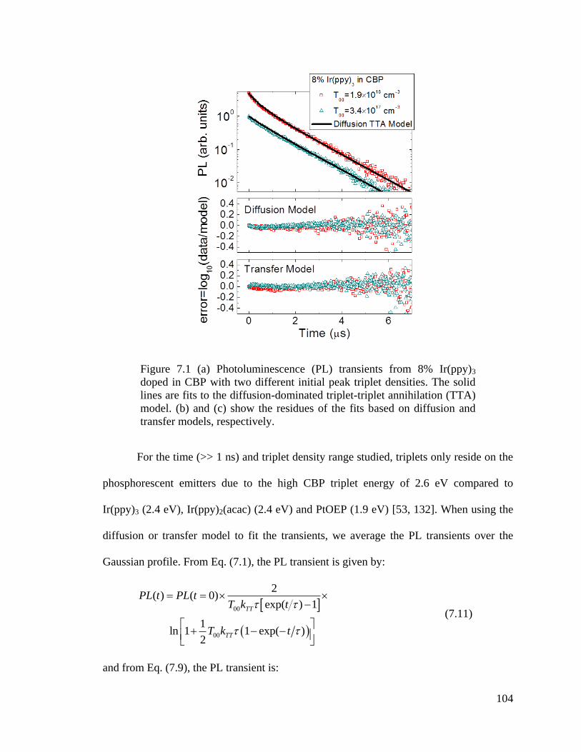
104
For the time (>> 1 ns) and triplet density range studied, triplets only reside on the
phosphorescent emitters due to the high CBP triplet energy of 2.6 eV compared to
Ir(ppy)3 (2.4 eV), Ir(ppy)2(acac) (2.4 eV) and PtOEP (1.9 eV) [53, 132]. When using the
diffusion or transfer model to fit the transients, we average the PL transients over the
Gaussian profile. From Eq. (7.1), the PL transient is given by:
00
00
2( ) ( 0)
exp( ) 1
1ln 1 1 exp( )
2
TT
TT
PL t PL tT k t
T k t
(7.11)
and from Eq. (7.9), the PL transient is:
Figure 7.1 (a) Photoluminescence (PL) transients from 8% Ir(ppy)3
doped in CBP with two different initial peak triplet densities. The solid
lines are fits to the diffusion-dominated triplet-triplet annihilation (TTA)
model. (b) and (c) show the residues of the fits based on diffusion and
transfer models, respectively.

105
2 2 /
00
2 2 / 2 2 /
00 00
2 / 2 /
2( ) ( 0)
1
1 1ln 1
2 2
t
TT
t t
TT TT
t t
PL t PL tT e
T e T e
e e
, (7.12)
where ( )PL t is the PL intensity proportional to total triplet population at time, t. We
restrict the fit parameters , TTk (diffusion model) or TT (transfer model) to be
constant for a given film under different initial triplet densities, 00T . The fit results from
all films are summarized in Table 7.1. Figure 7.1 (b) (c) show representative residues of
Table 7.1 Parameters for the PL transients fits using the diffusion and
transfer models
Vol
%
τ
(µs)
kTT
(10-13
cm3s
-1)
βTT
(10-30
cm6s
-1)
RFTT
(nm)
Ir(ppy)3 in CBP
2% 1.22±0.01 13±1 1.9±0.3 8.1
4% 1.19±0.01 21±1 3.3±0.4 8.9
8% 1.08±0.01 25±2 7.2±0.9 10.0
16% 0.94±0.01 36±4 17±3 11.2
Ir(ppy)2(acac) in CBP
2% 1.41±0.01 23±2 4.7±0.3 9.7
4% 1.22±0.01 32±2 8.9±1.1 10.5
8% 1.02±0.01 39±3 9.3±2.0 10.3
16% 0.67±0.01 50±5 28.1±4.0 11.5
PtOEP in CBP
2% 98±2 0.13±0.02 (4.7±1.6)×10-3
6.2
4% 95±1 0.23±0.02 (7.7±1.5)×10-3
6.7
8% 88±1 0.41±0.03 (13±2)×10-3
7.2
16% 84±1 0.52±0.05 (9.4±2)×10-3
6.8

106
the fits to Eq. (7.11) and (7.12), respectively. The residues are small in both cases, and
hence the two models cannot be distinguished based only on the fits.
7.2 Diffusion vs. Transfer Dominated Triplet Annihilation
From the transfer model results in Table 7.1, FTTR can be calculated from and
Figure 7.2 Triplet absorption cross-section spectra for Ir(ppy)3 (top) and
PtOPE (bottom) doped at different concentrations in CBP.

107
TT using Eq. (7.10), and is also shown in Table 7.1. The two Ir complexes show
comparable FTTR ranging from 8 nm to 12 nm, while the Pt complex shows a somewhat
smaller FTTR ≈ 7nm. In all three cases, there is an increasing trend in FTTR with doping
concentration.
To understand the fit results, FTTR can be estimated from Eq. (7.4) using the
triplet emission and triplet absorption spectra. Figure 7.2 shows the triplet absorption
spectra of Ir(ppy)3 and PtOEP doped at different concentrations in CBP measured using
the spatially separated pump-probe method [184]. Note that the PtOEP triplet absorption
spectrum is similar in shape to that reported by Ponterini, et al. [185] for PtOEP in
tetrahydrofuran solution, and close to the estimation of Staroske, et al. [177]. The spectra
overlap between the triplet emission and absorption are plotted in Figure 7.3. Thus, using
Figure 7.3 Molar absorptivity of triplets of Ir(ppy)3 (open square) and
PtOEP (open circle), as well as the corresponding PL spectra (lines).
The spectra are measured from films at 8% doping concentration in CBP,
although they are insensitive to doping (see Fig. 7.2).

108
literature values for ΦPL (~100% for the Ir-complexes [53, 186, 187] and ~25% for
PtOEP [52, 55]), the Förster radius is calculated from Eq. (7.4) to be FTTR = 3.1 nm for
Ir(ppy)3 and 2.7 nm for PtOEP.
Both the PL and triplet absorption are insensitive to doping concentrations [188].
Hence, the concentration dependence of FTTR in Table 7.1 cannot be understood from the
Förster transfer theory in Eq. (7.4). Furthermore, FTTR obtained from the PL transient fits
(Table 7.1) is larger than the calculation (in the previous paragraph) by a factor of 2 to 3,
leading to 100-1000 times discrepancy in 6 or ~FTT TT FTTk R (c.f. Eq. (7.10)). We note
that although the cubic lattice model in Eq. (7.8) is an approximation, the significant
difference between our fit and calculated FTTk clearly invalidates the transfer model.
Even at emitter concentrations as low as 0.1%, Staroske et al. [177] observed a factor of
1.44 discrepancy in Förster radii calculated from Eq. (7.4) and directly measured from PL
transients, leading to nearly 10 times difference in Förster transfer rate. This large
discrepancy was not considered significant by those authors.
The exciton diffusion model is based on triplet hopping from an excited to an
unexcited emitter molecule. Two energy transfer mechanisms can be responsible for such
hopping, Förster or Dexter-type [112, 163, 180], leading to two corresponding
expressions for diffusivity:
622 F
F FH
RaD a k
a
(7.13)
and 2 2 2
expD DH
aD a k a KJ
L
, (7.14)

109
where FD and DD are diffusivities due to Förster and Dexter transfer respectively, FHk
and DHk are the corresponding hopping rates to a nearest neighbor, a is the dopant lattice
constant related to C through 31/a CN , where N = 1021
cm-3
is the film molecular
density, FR is the triplet-to-ground-state Förster radius, K is related to exchange
interaction Hamiltonian, J is the density of states for energy transfer, and L is the
effective Bohr radius. It is clear that the two mechanisms lead to significantly different
functional dependence of D on a.
The experimental dependence of D on a can be derived from Eq. (7.2) and TTk
(see Table 7.1). Assuming CR is independent of a, then Eqs. (7.2), (7.13), and (7.14)
Figure 7.4 Comparison between two triplet diffusion mechanisms,
Förster transfer (with 1/a6 dependence) and Dexter transfer (exponential
dependence on a). The TTA rate constants, TTk , are obtained from PL
transient fit parameters in Table 7.1. The hopping rates, Hk , on the right-
hand ordinate are calculated assuming a capture radius of 1 nm. Note
that the data for PtOEP are multiplied by 50.

110
suggest that 2/TTk a ~ 61/ a for Förster-mediated diffusion, and follows an exponential
function for Dexter diffusion. A comparison of the behavior of kTT vs. a for the two
mechanisms is shown in Fig. 7.4. For all three emitters, the data are consistent with
Dexter diffusion; a conclusion consistent with Namdas, et al. [189] and Ribierre, et al.
[176] for TTA in Ir-cored dendrimers. Assuming CR = 1 nm, we also calculate the
hopping rate 2
6
8
TTH
kk
a on the right-hand ordinate of Fig. 7.4. From this we can estimate
the average number of hopping steps that a triplet makes before collision with a second
triplet by Hk [176]. This process varies between 3 and 30 steps, depending on the
doping concentration.
7.3 Emitter Design for High Brightness PHOLEDs
Interestingly, from Eq. (7.14), DD and thus TTk should be independent of ;
however, TTk for the two Ir-complexes is ~100 times greater for the Ir-complexes than
for PtOEP, while their radiative lifetimes are only 1% of the PtOEP lifetime. This inverse
correlation can be understood by evaluating J in Eq. (7.14) given by [112, 134]:
0
( ) ( )T SJ F E E dE (7.15)
where 0( )S E is the absorption cross-section of the emitter molecular ground state.
Figure 7.5 shows absorption of a solution of Ir(ppy)3, Ir(ppy)2acac, or PtOEP
dissolved in toluene at a concentration of 10-5
M. Here, diluted solution is adopted
because a direct measurement of emitter absorption in host/emitter thin films is difficult,

111
and photophysical properties for these phosphorescent emitters’ solutions typically
resemble the amorphous films [190-192]. From the PL and absorption spectral overlaps
(inset of Fig. 7.5), we find that 3(Ir(ppy) ) 50 (PtOEP)J J . Since TTk DD K J
(Eq. (7.2) and (7.14)), then the difference in J between Ir(ppy)3 and PtOEP must
contribute to the observed ~100 times differences in the corresponding TTk . On the other
hand, Ir(ppy)3 and Ir(ppy)2acac have very similar spectral overlaps, which is consistent
with their comparable kTT values (Table. 7.1). That is, J for PtOEP is significantly smaller
compared to that of the Ir-complexes because its absorption due to 0S T transition is
weaker as a result of its reduced metal-ligand-charge-transfer (MLCT) contribution to the
optical transitions characteristics of planar Pt compounds [51, 52, 190, 192].
Figure 7.5 Absorption spectra of Ir(ppy)3, Ir(ppy)2acac, and PtOEP
dissolved in toluene, shown only in the wavelength range of their
corresponding PL spectra. The spectral overlap (or the product of the
absorption and PL spectra at each photon energy) between the thin film
PL and absorption in solution are shown in the inset.

112
Since the “onset” current density for the roll-off in OLED efficiency at high
current densities due to TTA is proportional to 21 TTk (see section 2.3 or [116]), the
Dexter diffusion mechanism (Eqs. (7.2) and (7.14)) suggests that improved performance
at high brightness is possible if and TTk can be independently minimized. Figure 7.6
shows the calculated efficiency roll-off from Table 7.1 through Eq. (2.49) due to TTA for
three PHOLEDs with 30 nm of EMLs consisting of (1) 8% Ir(ppy)3:CBP, (2) 8%
PtOEP:CBP, and (3) an ideal EML with τ of 8% Ir(ppy)3:CBP and kTT of 8% PtOEP:CBP.
It is evident that simultaneous minimization of and TTk is desirable for PHOLEDs
operating at high current density (or luminance).
One means to accomplish this requires a high MLCT contribution to emission
(leading to low ) [134, 183] with a correspondingly large Stokes shift in the MLCT
Figure 7.6 Calculated PHOLED efficiency roll-off due to TTA based on
the parameters in Table 7.1. The ideal case is for an PHOLED emissive
layer with triplet lifetime of 8% Ir(ppy)3 in CBP and triplet-triplet
annihilation rate of 8% PtOEP in CBP.

113
absorption (leading to low TTk ). Previously [183], the importance of this Stokes shift has
not been emphasized in phosphorescent emitter design since self-absorption is
insignificant in PHOLEDs with doping concentrations and film thicknesses optimized for
high efficiency emission.
The results here are in stark contrast to that of Staroske et al. [177], who conclude
that TTA is dominated by triplet-to-triplet energy transfer, and proposed minimizing TTA
through reducing the phosphorescent emitter PL and triplet-triplet absorption (from T to
a higher triplet excited state) spectral overlap. Although at low emitter concentrations (<
1%), triplet-to-triplet energy transfer is more likely to dominate due to suppressed
diffusion, the calculated [177] triplet-to-triplet transfer rate is off by nearly a factor of 10.
In conclusion, transient PL measurements in three prototype phosphorescent
emitters suggests that TTA is dominated by triplet diffusion, and that direct triplet-to-
triplet energy transfer [177], plays a considerably smaller role. Further, the diffusion of
triplets follows the Dexter exchange interaction, in which the TTA rate is independent of
triplet lifetime. Therefore, while maintaining the low triplet lifetime desirable for low
efficiency roll-off in PHOLEDs, a reduced TTA rate can be achieved through decreasing
the spectral overlap between the phosphorescent emitter absorption and emission. This
understanding of energy transfer can be used to design efficient PHOLED emitters with
reduced efficiency roll-off at high brightness.

114
Chapter 8
Controlling Triplet Dynamics to Extend the
Operational Lifetime of Blue PHOLEDs
In previous chapters we studied exciton-exciton annihilation and its effects on the
efficiency of OLEDs. Besides efficiency, operational lifetime is another significant
figure-of-merit for OLED technology to gain commercial acceptance. Phosphorescent
OLEDs (PHOLEDs) can harvest 100% of the electrical excitations, thereby having a
significantly higher efficiency than fluorescent OLEDs. Unfortunately, the blue sub-
pixels in OLED displays employ fluorescent OLEDs due to the short operational lifetime
in blue PHOLEDs. In Section 8.1, we introduce the topic of OLED lifetime and review
previous research on the degradation mechanisms of blue PHOLEDs. It has been
suggested by Giebink et al. [193, 194] that triplet-polaron annihilation (TPA) between a
triplet on the phosphorescent dopant and a polaron on the conductive host is the primary
source of intrinsic degradation in blue PHOLEDs. In section 8.2, a novel PHOLED
architecture is designed where the emissive layer (EML) consists of a linearly graded
concentration phosphorescent dopant concentration profile. Grading results in low
exciton density and thus suppressed TPA, leading to a significantly extended operational
lifetime over conventional blue PHOLEDs. When two blue PHOLEDs are placed in a

115
series stack, as shown in section 8.3, this strategy leads to a 10-fold operational lifetime
improvement over a conventional blue PHOLED.
8.1 Blue PHOLEDs Operational Lifetime: an Introduction
When an OLED operates under constant current with an initial luminance of L0,
its operational lifetime (TX(L0)) is defined by the degradation time for the device
efficiency to drop to X% of the initial efficiency. During the OLED luminance decay, its
operational voltage continuously increases. Also, TX(L0) decreases as L0 increases.
Early reported OLED lifetimes based on Alq3 as emitters are short. For example,
Van Slyke et al. [195] reported a T60(510 cd/m2) ≈ 3000 hrs, and Aziz et al. [196]
Table 8.1 Commercial OLED efficiency and lifetime
CIE Efficiency (cd/A) T50 (1000 cd/m2)
Phosphorescent OLEDs*
Deep Red [0.69, 0.31] 17 250,000
Red [0.64, 0.36] 30 900,000
Yellow [0.44, 0.54] 81 1,450,00
Green [0.31, 0.63] 85 400,000
Cyan [0.18, 0.42] 50 20,000
Fluorescent OLEDs**
Red [0.67, 0.33] 11 160,000
Green [0.29, 0.64] 37 200,000
Blue [0.14, 0.12] 9.9 11,000
*data from Universal Display Corp. http://www.udcoled.com/ (2014)
**data from Idemitsu http://www.idemitsu.com/ (2014)

116
reported a T50(1050 cd/m2) ≈ 1000 hrs. After more than a decade of research, significant
breakthroughs in green and red OLEDs lifetime have been achieved, with reported
T50(1000 cd/m2) exceeding 10
6 hr [197-200]. Table 8.1 summarizes commercially
produced OLED efficiencies and lifetimes. It is evident that red and green PHOLEDs are
superior to analogous fluorescent OLEDs in both efficiency and lifetime. In contrast,
progress in the improvement of blue PHOLED lifetime has been slow. For example, a
T50(1000 cd/m2) of only several hours has been reported for a PHOLED with the blue
emitting iridium (III) bis[(4,6-difluorophenyl)-pyridinato-N,C2’
] picolinate (FIrpic) [201]
as the emitter [202]. As a result, relatively inefficient blue fluorescent OLEDs remain
dominant in OLED displays.
Factors leading to OLED degradation [31, 194, 196, 203] can be divided into two
categories: extrinsic and intrinsic. Extrinsic factors include impurities in the molecules
used for device fabrication, water and/or oxygen residues in the evaporation chamber
(when pressure > 5×10⁻⁸
Torr), air leakage into the device package post-fabrication, etc.
Intrinsic factors include molecular degradation (for example, bond cleavage) and organic
film morphology change caused by charge transport, exciton non-radiative decay,
Table 8.2 Common molecular bond energy [3]
Bond Energy (eV) Bond Energy (eV)
C-C 3.64 N-N 1.69
C-H 4.28 N-O 2.08
C-O 3.71 N-H 4.05
C-N 3.04 O-O 1.51
C-F 5.03 H-H 4.52

117
exciton-exciton annihilation, and exciton-polaron annihilation. Table 8.2 lists common
molecular bond energies. It is clear that these energies (for example C-C, C-H, C-N)
exceed 3 eV, which is higher than the first excited singlet or triplet energies typical in
OLED materials. However, during exciton interactions (i.e. exciton-exciton or exciton-
polaron annihilations), there is a possibility that twice the exciton energy can be
thermally relaxed simultaneously onto a molecule, thereby breaking the bond.
Previously, Giebink et al. studied the degradation of a blue PHOLED with
iridium (III) tris[3-(2,6-dimethylphenyl)-7-methylimidazo[1,2-f] phenanthridine]
(Ir(dmp)3) doped in 4,4’-bis(3-methylcarbazol-9-yl)-2,2’-biphenyl (mCBP) as the
emissive layer (EML). It was found that bimolecular triplet-polaron annihilation (TPA) is
the intrinsic degradation mechanism in the blue PHOLED. As illustrated in Fig. 8.1,
during TPA, the high energy blue triplet on Ir(dmp)3 transfers its energy to a polaron on
mCBP, thereby exciton the polaron to a higher energy (i.e. as high as 6 eV) hot polaron
Figure 8.1 Illustration of triplet-polaron annihilation (TPA) and the
formation of hot polaron. The hot polaron has approximately twice the
triplet energy, which is enough to break molecular bonds.

118
state. The hot polaron, on thermalization, can break bonds on the molecule on which it
resides, thus forming a defect in the EML, which can subsequently quench excitons as
well as trap charges. The quantitative analysis of TPA induced PHOLED degradation is
discussed in Section 8.3.
Due to their high triplet energy, excess energy dissipated through TPA in blue
PHOLEDs is significantly higher than for red or green PHOLEDs, explaining the more
rapid degradation in the former case. Furthermore, while blue fluorescent devices are by
no means immune to this degradation path, their lower triplet energy leads to a
proportionately greater probability for destructive exciton-polaron annihilation events to
occur in phosphorescent devices.
8.2 Management of the Exciton Profile in PHOLEDs
While little progress has been made since these fundamental mechanisms were
identified, it is possible that a route to reduce degradation via TPA is to decrease the
exciton density in the PHOLED exciton formation zone. Recently, Erickson and Holmes
[204] have demonstrated increased efficiency by the extension of the exciton formation
zone in a green PHOLED from 15 nm to > 80 nm through graded mixing of electron and
hole transporting host molecules. No lifetime data were reported in that work.
Furthermore, the selection of stable host materials with high triplet energies for blue
PHOLEDs is limited. Use of continuously or stepwise graded phosphorescent dopant
profile in OLEDs was previously reported [205-207] to improve the OLED efficiency;

119
however, it is unclear whether the OLEDs exciton formation zones were extended in
these reports and lifetime data were also unavailable.
In this section, we show that grading the blue dopant in the emitting layer (EML)
of a PHOLED significantly extends the lifetime of the device by extending the exciton
formation zone. The broadening of the exciton distribution, and hence the device lifetime,
is further increased by using a sufficiently high dopant concentration, and with the dopant
highest occupied molecular orbital level (HOMO) chosen above that of the host to allow
for holes to conduct directly on the dopant. To our knowledge, this is the first report of an
OLED with a graded doping profile that extends the distribution of excitons within the
EML, thus significantly impacting device operational lifetime.
For this demonstration, we use the previously reported [194] blue dopant and host
combination of Ir(dmp)3 and mCBP, respectively. We compare three PHOLEDs (shown
in Fig. 8.2) with the structures of 120 nm ITO/ 10 nm HATCN/ 50 nm X/ 5 nm mCBP/
30 nm Alq3/ 1.5nm Liq/ 100 nm aluminum:
in D1, X is 20 nm NPD/ 30 nm 13 vol% Ir(dmp)3 doped in mCBP;
in D2, X is 50 nm 13 vol% Ir(dmp)3 doped in mCBP;
in D3, X is 50 nm 188 vol% graded Ir(dmp)3 doped in mCBP;
where ITO (indium-tin-oxide) is the anode, HATCN (hexaazatriphenylene
hexacarbonitrile) is the hole injection layer (HIL), NPD (4,4’-bis[N-(1-naphthyl)-N-
phenyl-amino]-biphenyl) is the hole transport layer (HTL), Ir(dmp)3 doped mCBP is the
EML, mCBP is the hole blocking layer (HBL), Alq3 (tris(8-hydroxyquinolinato)
aluminum) is the electron transport layer (ETL), Liq (8-hydroxyquinolinato lithium) is
the electron injection layer (EIL), aluminum is the cathode. Device D4 is a two-unit

120
stacked OLED (SOLED) with the structure: 120 nm ITO/ 10 nm HATCN/ 50 nm EML/ 5
nm mCBP/ 5 nm Alq3/ 70 nm 2 vol% Li doped Alq3/ 10 nm HATCN/50 nm EML/ 5 nm
mCBP/ 25 nm Alq3/ 1.5 nm Liq/ 100 nm aluminum, where the EMLs of the PHOLEDs
comprising the stack are analogous to D3
Devices D1-D4 were deposited by thermal evaporation on pre-cleaned indium tin
oxide (ITO)-on-glass substrates in a system with a background pressure of ~5×10⁻⁷
Torr.
The PHOLEDs are packaged in an ultrahigh purity N2-filled glovebox with < 0.5 ppm
Figure 8.2 Structures of the blue phosphorescent organic light emitting
diodes (PHOLEDs). Hexaazatriphenylene hexacarbonitrile (HATCN),
4,4’-bis[N-(1-naphthyl)-N-phenyl-amino]-biphenyl (NPD) and tris(8-
hydroxyquinolinato)aluminum (Alq3) are used for the hole injection
(HIL), hole transport (HTL), and electron transport layer (ETL)
materials, respectively. The EMLs of both D1 and D2 employ a 13 vol%
doping concentration, and D2 replaces the HTL in D1 with EML. D3 has
an EML with the doping concentration graded from 18 to 8 vol% with a
maximum at the EML/HIL interface. D4 is a stacked OLED with two
EMLs identical to D3.

121
oxygen and water concentration without exposure to air following film deposition, by
attaching a glass lid to the substrate using an epoxy seal around the perimeter. Here, D1 is
almost identical to the blue PHOLED reported previously [194], and serves as the control
device.
Figure 8.3 Performance characteristics of the blue PHOLEDs. (a)
Current density-voltage (J-V, scattered markers) and luminance-voltage
(L-V, line-connected markers) characteristics for D1-D4, where D4 is a
stack of two blue emitting PHOLED whose EMLs are identical to D3.
(b) External quantum efficiency (EQE) v.s. J (left axis) and emission
spectra (right axis) for D1-D4.
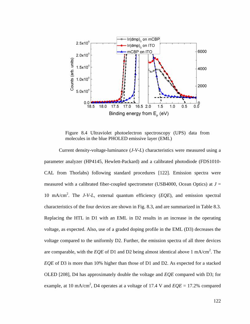
122
Current density-voltage-luminance (J-V-L) characteristics were measured using a
parameter analyzer (HP4145, Hewlett-Packard) and a calibrated photodiode (FDS1010-
CAL from Thorlabs) following standard procedures [122]. Emission spectra were
measured with a calibrated fiber-coupled spectrometer (USB4000, Ocean Optics) at J =
10 mA/cm2. The J-V-L, external quantum efficiency (EQE), and emission spectral
characteristics of the four devices are shown in Fig. 8.3, and are summarized in Table 8.3.
Replacing the HTL in D1 with an EML in D2 results in an increase in the operating
voltage, as expected. Also, use of a graded doping profile in the EML (D3) decreases the
voltage compared to the uniformly D2. Further, the emission spectra of all three devices
are comparable, with the EQE of D1 and D2 being almost identical above 1 mA/cm2. The
EQE of D3 is more than 10% higher than those of D1 and D2. As expected for a stacked
OLED [208], D4 has approximately double the voltage and EQE compared with D3; for
example, at 10 mA/cm2, D4 operates at a voltage of 17.4 V and EQE = 17.2% compared
Figure 8.4 Ultraviolet photoelectron spectroscopy (UPS) data from
molecules in the blue PHOLED emissive layer (EML)

123
to 8.5 V and 9.3% for D3. This indicates a slight but measurable loss in the stacked
device due to inefficiencies in charge generation in the layers between the stacked
elements, and in the optical field distribution within the stack [209].
To understand the charge transport characteristics in the various EMLs, ultraviolet
photoelectron spectra (UPS) were measured in an ultrahigh vacuum (UHV) analysis
chamber using the illumination from the He Iα line with 21.2 eV of energy. Figure 8.4
shows the UPS from 50 nm thick layers of mCBP and Ir(dmp)3 on ITO, and 50nm-
Ir(dmp)3-on-50nm-mCBP on ITO. The highest occupied molecular orbital energies
(HOMOs) of mCBP and Ir(dmp)3 are 6.0±0.1 eV and 4.6±0.1 eV respectively. A dipole
energy shift of ~0.4 eV is observed when Ir(dmp)3 is deposited on mCBP, and thus the
HOMO of Ir(dmp)3 is 5.0±0.1 eV on mCBP.
Table 8.3 Characteristics at L0 = 1000 cd/m2 for blue emitting PHOLEDs
*
L0=1000 cd/m2
CIE**
EQE
(%)
J
(mA/cm2)
V
(V)
T80
(hr)
T50
(hr)
D1 [0.16, 0.31] 8.5±0.1 6.2 6.9±0.2 56±3 510±15
D2 [0.16, 0.31] 8.5±0.2 6.2 8.7±0.3 - -
D3 [0.16, 0.31] 9.5±0.1 5.7 7.7±0.2 213±5 1500†/1600
‡
D4 [0.15, 0.29] 18.0±0.2 2.9 14.3±0.1 616±10 3500†/3700
‡
* errors for EQE and V are standard deviations from at least 6 devices, errors for T80
and T50 are standard deviations from 3 devices
** Measured at 10 mA/cm2
† Estimated from extrapolations using the triplet-polaron annihilation (TPA) model
‡ Estimated from extrapolation using the adjusted exponential (empirical) model
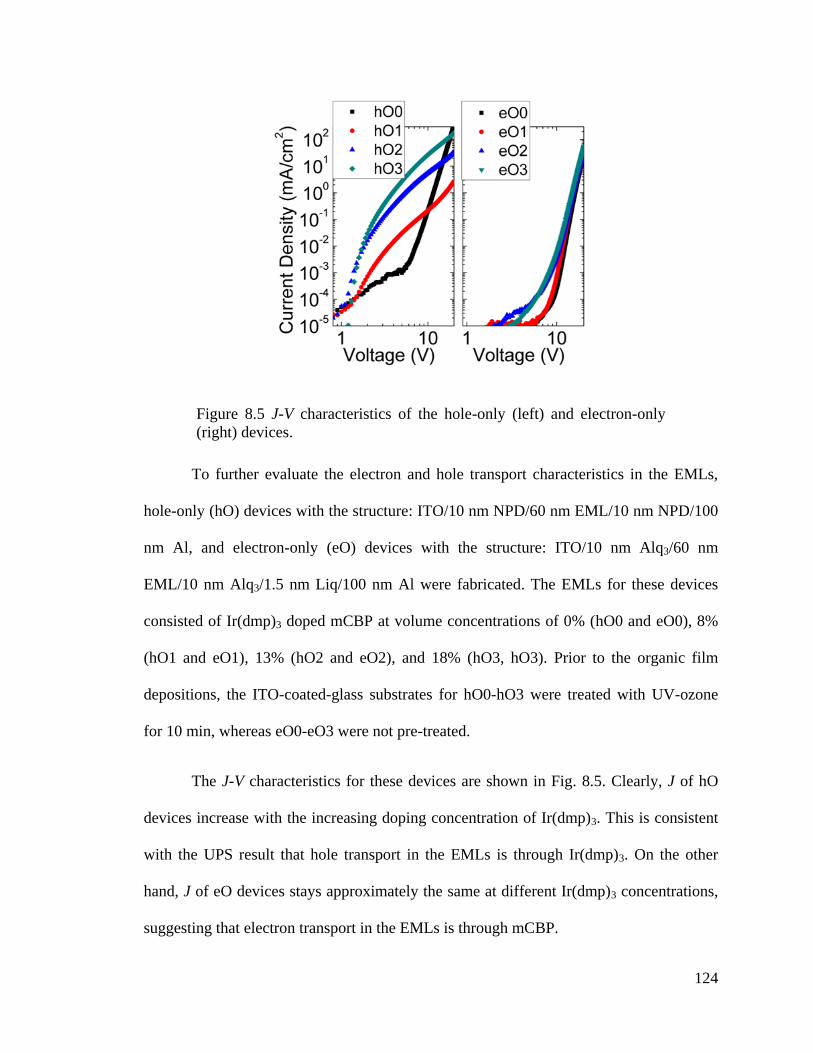
124
To further evaluate the electron and hole transport characteristics in the EMLs,
hole-only (hO) devices with the structure: ITO/10 nm NPD/60 nm EML/10 nm NPD/100
nm Al, and electron-only (eO) devices with the structure: ITO/10 nm Alq3/60 nm
EML/10 nm Alq3/1.5 nm Liq/100 nm Al were fabricated. The EMLs for these devices
consisted of Ir(dmp)3 doped mCBP at volume concentrations of 0% (hO0 and eO0), 8%
(hO1 and eO1), 13% (hO2 and eO2), and 18% (hO3, hO3). Prior to the organic film
depositions, the ITO-coated-glass substrates for hO0-hO3 were treated with UV-ozone
for 10 min, whereas eO0-eO3 were not pre-treated.
The J-V characteristics for these devices are shown in Fig. 8.5. Clearly, J of hO
devices increase with the increasing doping concentration of Ir(dmp)3. This is consistent
with the UPS result that hole transport in the EMLs is through Ir(dmp)3. On the other
hand, J of eO devices stays approximately the same at different Ir(dmp)3 concentrations,
suggesting that electron transport in the EMLs is through mCBP.
Figure 8.5 J-V characteristics of the hole-only (left) and electron-only
(right) devices.

125
In this unusual architecture, as shown in Fig. 8.6 (a) recombination occurs
between an electron in the lowest unoccupied molecular orbital (LUMO) of mCBP, and a
hole in the Ir(dmp)3 HOMO, resulting in an exciplex. Since the PHOLED emission is
solely from the phosphorescence of Ir(dmp)3, the intermediate exciplex state rapidly
transfers its energy to the Ir(dmp)3 triplet. Note that the thermalization loss when an
electron on mCBP recombines with a hole in Ir(dmp)3 HOMO is 1.0 eV less than for a
Figure 8.6 Energetics and exciton density profiles in the PHOLED EML.
(a) Electron and hole transport and recombination energetics in the blue
PHOLED EMLs. (b) Exciton density profile in the EMLs of D1-D3
calculated from “probe” devices employing iridium (III) bis(2-phenyl
quinolyl-N,C2’
) acetylacetonate (PQIr) in the red light emitting sensing
layer. The profiles are normalized to integrated exciton densities in the
EMLs of unity. Also, the exciton density profile of D4 is calculated from
the D3 profile.

126
hole in the mCBP HOMO, contributing to the relatively high operational stability in the
blue PHOLEDs observed previously[194], and in D1 (see below).
The hole conductivity in the graded EML of D3 increases as the distance to the
HIL/EML interface is decreased due to the increasing concentration of Ir(dmp)3. In the
opposite direction toward the EML/HBL interface, the hole conductivity decreases while
the electron conductivity stays approximately constant. Thus, in contrast to the abrupt
hole blocking by the EML/HBL interface in D1 and D2, in D3 the holes are gradually
blocked by the hole conductivity gradient. As a consequence, exciton formation in D3
occurs over a more extended distance as compared to either D1 or D2.
To determine the hole blocking efficiency and thus the shape of the exciton
formation zones in D1-D3, we fabricated a series of PHOLEDs with a thin, red emitting
“sensing” layer using the dopant, iridium (III) bis(2-phenyl quinolyl-N,C2’
)
acetylacetonate (PQIr) whose relative emission intensity can provide information about
the spatial distribution of excitons in the EML. Here, PQIr is co-doped at 2 vol% at
different positions separated by 5 nm in the EMLs of D1-D3, with a doping layer width
of 1.5 nm. The HOMO and LUMO energies of PQIr are at 5.0 eV and 2.7 eV relative to
the vacuum level, respectively [210]. Due to the low doping concentration and
narrowness of the sensing layers, it should not significantly affect the charge transport or
recombination properties in the EML. This is confirmed by the almost identical J-V
characteristics between devices with and without sensing layers.
Local exciton densities N(x) in the EMLs can be calculated from the measured
emission spectra, external quantum efficiency, EQE(x), and the calculated out-coupling

127
efficiency ( )R x (at a wavelength of 595 nm corresponding to the peak in the PQIr
emission spectrum), from PHOLEDs with PQIr sensing layer at position x using:
( ) 1
( ) ( )( ) ( ) ( )
out
R
out out
R B R
N xN x A EQE x
N x N x x
. (8.1)
Here, A is a normalization factor such that ( ) 1EML
N x dx , ( ) ( )out out
R BN x N x is the out-
Figure 8.7 (top) Emission spectra from probe devices for D2 at J = 10
mA/cm2. (bottom) Parameters for calculating the exciton density profiles
(see Eq. 8.1).

128
coupled photon number ratio from PQIr versus Ir(dmp)3, obtained from the ratio of red
(IR) and blue (IB) peaks of the emission spectra through ( ) 595nm
( ) 466nm
out
R R
out
B B
N x I
N x I .
Representative emission spectra are shown in Fig. 8.7 (a) from the devices for the EML
employed in D2. In Fig. 8.7 (b), we show EQE(x) (at J = 10 mA/cm2),
( )( )
( ) ( )
out
R
out out
R B
N xr x
N x N x
(at J = 10 mA/cm
2), and ( )R x (calculated following Celebi et
al. [211]) for the sensing OLEDs for D1-D3.
The calculated N(x) from Eq. (8.1) is shown in Fig. 8.6 (b). In D1 (i.e. the
conventional blue PHOLED), significant exciton accumulation occurs at the EML/HBL
interface. In D2 where there is no HTL, the exciton density at the HIL/EML interface is
reduced due to a correspondingly low concentration of holes. However, because of the
reduced hole transport efficiency, electrons penetrate deep into the EML, resulting in a
peak exciton density near the HIL/EML interface. In contrast, both efficient hole
transport near the HIL/EML interface and the gradual hole blocking in the EML in D3
lead to a more uniform exciton distribution (and hence higher EQE) compared to D1 and
D2, with a peak density near to the center of the EML. Since the EMLs of D3 and D4 are
identical, also shown in Fig. 8.6 (b) is the exciton density profile of D4, estimated at 53%
of the exciton density in D3 (at 10 mA/cm2) due to the almost double EQE.

129
8.3 Ten-fold Improvement in the Lifetime of Blue PHOLEDs
Figure 8.8 shows the time evolution of the luminance, L, and the change in
voltage from its initial value, ΔV = |V(t=0)-V(t)|, for D1, D3, and D4 tested at room
temperature and a constant current density for two initial luminances: L0 = 1000 and 3000
cd/m2. Also, we show these same characteristics for D2 tested at L = 3000 cd/m
2. The
lifetimes show an increasing trend from D1 through D4. For example, T80(3000 cd/m3) =
11.5, 24.5, 39, and 106 hr, respectively, for D1-D4, consistent with the broadened exciton
formation zone of the latter two devices (Fig. 8.6 (b)). Note that T80 for the control is
consistent with similar results for this device reported previously6, and is only ~29% that
of the graded device, D3. Further, T80(1000 cd/m2)= 616±10 hr for D4, representing a
more than 10 times improvement from the previously investigated [194] control, D1. The
improvement in T50 for D4 is slightly less significant than T80, leading to an
approximately seven-fold increase from D1.
To establish a quantitative relationship between the exciton density profiles and
operational lifetimes, we model L and ΔV as functions of time, t, following the model of
Giebink et al. [194]. The model considers trap (with density Q(x, t)) formation due to
TPA, and subsequent interactions with electrons with density n(x, t), holes with density
p(x, t), and excitons with density N(x, t):
( ) ( , ) ( , ) ( , ) ( , ) 0L QnG x k n x t p x t k Q x t n x t (8.2)
( ) ( , ) ( , ) ( , ) ( , ) 0L QpG x k n x t p x t k Q x t p x t (8.3)
1( , ) ( , ) ( , ) ( , ) 0L QT
N
k n x t p x t k Q x t N x t
(8.4)

130
where kL is the Langevin recombination rate, kQn is the trap-electron interaction rate, kQp
is the trap-hole interaction rate, kQT is the trap-triplet annihilation rate, N is the triplet
lifetime, and and G(x) is the local recombination rate, calculated from the local exciton
density N(x) using( )
( )( )
J N xG x
e N x dx
, where e is the electron charge. Current densities
at L0 = 1000 cd/m2 are provided in Table 1, and at 3000 cd/m
2 are J = 21, 21, 17.5, and
9.1 mA/cm2 for D1, D2, D3, and D4, respectively. Trap formation is attributed to TPA at
a rate of kQ using:
Figure 8.8 Time evolution of the normalized luminance, L, of blue PHOLEDs
and change in operating voltage ΔV (offset to zero) at the initial luminance of L0
= 3000 cd/m2 ((a) and (b)) and 1000 cd/m
2 ((c) and (d)). The data are fit to a
triplet-polaron annihilation (TPA) model using the exciton density profiles in
Fig 3 (b). The luminance for L0 = 1000 cd/m2 (c) are also fit to the adjusted
exponential (empirical, or EMP) model to estimate T50 (i.e. degradation time
leading to 50% decrease in L0).

131
( , )
( , ) ( , )Q
dQ x tk N x t n x t
dt (8.5)
Then, the OLED degradation can be calculated through,
( ) ( , ) ( )BL t B N x t x dx (8.6)
0
( ) (0) ( , )e
V t V xQ x t dx
(8.7)
where B is a normalization factor, ( )B x is the calculated out-coupling efficiency (for
Ir(dmp)3 emission peaked at 466 nm), = 3 is the relative permittivity, and 0 is the
vacuum permittivity.
The model is fit to the degradation of D1-D4 with kQ and kQT as free parameters;
all other parameters are as previously determined for this materials combination [194]
(see Table 8.4). Yamamoto et al. [212] reported that water contamination of organic films
during deposition leads to an accelerated initial degradation when the deposition
background pressure is > 5×10⁻⁸
Torr for PHOLEDs almost identical to D1. In our case,
organic films were deposited in a system with a base pressure of 5×10⁻⁷
Torr. However,
the TPA model ignores extrinsic effects such as water contamination. To account for
these effects in our fits, t = 0 corresponds to a normalized luminance of 0.95, and the
initial value of ΔV was chosen to be nonzero (i.e. (0)V = 0.2 V (at 3000 cd/m2) and 0.3
V (at 1000 cd/m2) for D1-D3, and 0.1 V (at 3000 cd/m
2) and 0.15 V (at 1000 cd/m
2) for
D4.).
From Table 8.4, kQ and kQN in D1 and D2 are almost identical, suggesting that
improvement of the operational lifetime from D1 to D2 is simply a result of changes in

132
the exciton density profile. In D3, the significant increase in lifetime is due to the
increase in EQE (leading to a decrease of J to achieve a given L0), as well as to the
significant spreading of the exciton formation zone compared to the former devices. Note
that the TPA model considers degradation in the thin film bulk, but not at the interface
[213]. Indeed, the low exciton density at the EML/HBL interface in D3 may also
contribute to the observed increase in lifetime by reducing the rate of damage at this
interface.
To estimate T50(1000 cd/m2) for D3 and D4, we extrapolate the times obtained
from the TPA model fits. In addition, an empirical method often employed to model
OLED degradation uses the adjusted exponential decay function: [214]
L(t) = exp - t / t( )
béëê
ùûú
. Here, and are phenomenological parameters. This model
also results in reasonable fits to the degradation data (Fig. 8.8 (c)), and provides
extrapolated values for T50(1000 cd/m2) similar to those obtained from the physics-based
TPA model (Table 8.3). From these fits, T50(1000 cd/m2) = 3500 hr for D4, which
Table 8.4 Lifetime fitting parameters for blue emitting PHOLEDs
D1 D2 D3 D4
Triplet-polaron annihilation (TPA) model
Fixed parameters kQn = 1.44×10⁻¹³
cm3s
-1, kQp = 4.8×10
-14 cm
3s
-1,
kL= 1.7×10⁻¹³
cm3s
-1, τN = 1.1 µs
kQ (10-11
cm3s
-1) 1.0±0.1 1.1±0.1 0.95±0.1 0.9±0.1
kQT (10-24
cm3s
-1) 7±1 7±1 6±1 7±1
Adjusted exponential (empirical) model
τ (103 hrs) 1.03±0.01 - 2.96±0.04 6.74±0.10
β 0.54±0.01 - 0.58±0.01 0.63±0.01

133
approaches that of blue fluorescent OLEDs with T50(1000 cd/m2) ~ 10
4 hr (Table 8.1).
Note that the emission from D1-D4 is light blue (although more saturated than the cyan
color of FIrpic). However, color tuning to achieve more saturated blue emission is
commonly achieved in fluorescent blue display sub-pixels through the use of
microcavities[215, 216] and/or color filters. For example, a 70 nm thick anode of indium-
tin oxide (ITO) yields Commission Internationale d’Eclairage chromaticity coordinates of
[0.16, 0.26], compared to [0.16, 0.31] for a 120 nm thick ITO layer due to weak
microcavity effects.
Although the blue PHOLED lifetime reported here remains substantially less than
that of red and green PHOLEDs at similar luminances, blue sub-pixels in displays operate
at a considerably lower luminance than either the red or green sub-pixels. For example,
the required luminance to achieve an sRGB color gamut [217] for green is 9.9 times the
luminance for blue. Thus, a comparison between blue and green PHOLED lifetimes for
displays suggests that the blue PHOLED sub-pixel luminance needs to be only ~10% that
of the green. Under such conditions, the TPA model estimates the blue PHOLED lifetime
is T50(100 cd/m2) ≈ 70,000 hr. Also, adopting a degradation acceleration factor that
relates luminance to lifetime [214], viz.
22 2
50 50 2
1000cd/m(100 cd/m ) (1000 cd/m )
100cd/m
n
T T
and n = 1.55, the extrapolated blue
PHOLED lifetime is T50(100 cd/m2) ≈ 1.3×10
5 hr. These extrapolated lifetimes approach
the commercial green PHOLED lifetime of T50(1000 cd/m2) .
In summary, we demonstrated a ten-fold increase in blue PHOLED lifetime
employing an extended exciton formation zone achieved by grading the concentration
profile of the hole conducting phosphorescent dopant in the EML. Considering the

134
different color sub-pixel luminances used in displays, the improved blue PHOLED
lifetimes achieved in stacked devices approaches that of green PHOLEDs under normal
operating conditions. The novel device architecture employed is based on a fundamental
physical understanding of the relationship between energy-driven triplet-polaron
annihilation and device degradation, and hence should be generally applicable to a wide
range of phosphorescent and fluorescent devices. Further lifetime improvements are
anticipated by finding dopant/host combinations with conduction properties similar to the
materials used here, and that minimize interactions between triplets on the dopant and
polarons on the host molecules, therefore decreasing the probability of occurrence for
high energy TPA interactions that lead to molecular decomposition.

135
Chapter 9
Future Work
The field of organic electronics is still in its infancy compared to the mature field
of inorganic semiconductors. Many unique features of organics can be utilized for
applications that are difficult or impossible to achieve with inorganic materials. This
chapter explores the feasibility of two novel organic optoelectronic devices: a singlet
fission organic coating for photovoltaics and an electrically pumped organic
semiconductor laser.
9.1 A Singlet Fission Organic Coating for Photovoltaics
Singlet fission is a process where one singlet with high energy is converted to two
triplets with lower energy [166], and is the reverse (Auger-like) process of triplet-triplet
annihilation (TTA in Eq. 2.41). It is highly efficient in some organic materials and has the
potential of doubling the external quantum efficiency (EQE) and thus increasing the
power conversion efficiency (PCE) of organic photovoltaics (OPVs). However, although
OPVs with PCE > 10% [73] have been demonstrated over the past two years, they are
still far behind the inorganic PV performance.

136
A viable approach to combine the unique singlet fission process in organics and
achieve a high PCE in inorganic PVs is shown in Fig. 9.1. Here, a organic “fission
coating” is deposited on the front surface of an inorganic solar cell. The organic thin film
consists of two types of molecules, a singlet fission sensitizer doped with a
phosphorescent emitter. The fission sensitizer has a singlet energy higher than twice its
triplet energy to facilitate resonant exothermic singlet fission [166], and the
phosphorescent emitter has a lower triplet energy than the sensitizer. During operation,
the ultraviolet (UV) and blue part of solar spectrum is absorbed by the sensitizing layer,
where one singlet undergoes fission to form two triplets. The triplets on the sensitizer are
transferred to the phosphorescent emitter and then decays radiatively, resulting in red or
infrared (IR) emission subsequently absorbed by the inorganic PV. The green, red, and IR
Figure 9.1 Structure (a) and operation principle (b) of the proposed
singlet fission organic coating for photovoltaic applications.

137
part of the solar spectrum transmits through the organic film and is directly absorbed by
the inorganic PVs.
To evaluate the impact of this approach, we calculate the PV efficiency
improvement based on the singlet fission coating. The calculation is based on the detailed
balance approach of Shockley and Queisser [2] assuming that the organic film absorbs
100% of the solar spectrum above its bandgap of ESF, and emits photons with the energy
of ½ESF at 200% photoluminescence quantum efficiency. Also, the inorganic solar cell
bandgap is EG, and the organic film is transparent to photon energies below ESF. The
calculated PCE limit as a function of EG is shown in Fig. 9.2 for different ESF. It is
evident that the conventional SQ limit of 33.7% (black line) for single junction solar cell
can be improve to as high as 42% (blue line) for the case of ESF=2.2 eV and EG=1.1 eV.
Interestingly, this optimized inorganic band gap is the same as the bandgap of silicon.
Figure 9.2 Calculated maximum power conversion efficiency (PCE)
based on detailed balance theory [2] using an organic fission sensitizer
with the singlet energy of ESF on an inorganic photovoltaic (PV) cell
with a band gap of EG.

138
The next question is whether such a combination of organic fission sensitizer and
phosphorescent emitter already exists in the literature. Some promising combinations
include the use of diphenylisobenzofuran (ES=2.8 eV, ET=1.4 eV) [218] or diphenyl
tetracene (ES=2.5 eV, ET=1.2 eV) [191] as the fission sensitizer, and platinum complexes
such as tetraphenyltetranaphtho platinum porphyrins (ET=1.4 eV) [219, 220] as the
phosphorescent emitter. Indeed, although there are many efficient phosphors for visible
emission, highly efficiency infrared phosphorescent emitters are rarely reported in the
literature. This is possibly due to a lack of motivation for synthesizing such emitters up to
this time.
9.2 Feasibility of an Electrically Pumped OSL
Optically pumped organic semiconductor lasers (OSLs) were demonstrated more
Figure 9.3 Proposed structure for an OLED-pumped-OSL
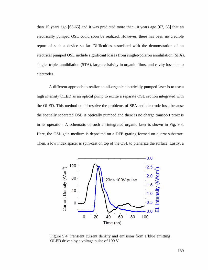
139
than 15 years ago [63-65] and it was predicted more than 10 years ago [67, 68] that an
electrically pumped OSL could soon be realized. However, there has been no credible
report of such a device so far. Difficulties associated with the demonstration of an
electrical pumped OSL include significant losses from singlet-polaron annihilation (SPA),
singlet-triplet annihilation (STA), large resistivity in organic films, and cavity loss due to
electrodes.
A different approach to realize an all-organic electrically pumped laser is to use a
high intensity OLED as an optical pump to excite a separate OSL section integrated with
the OLED. This method could resolve the problems of SPA and electrode loss, because
the spatially separated OSL is optically pumped and there is no charge transport process
in its operation. A schematic of such an integrated organic laser is shown in Fig. 9.3.
Here, the OSL gain medium is deposited on a DFB grating formed on quartz substrate.
Then, a low index spacer is spin-cast on top of the OSL to planarize the surface. Lastly, a
Figure 9.4 Transient current density and emission from a blue emitting
OLED driven by a voltage pulse of 100 V

140
blue or green emitting OLED with a semitransparent bottom electrode and a reflective
top electrode is grown on top of the spacer.
To evaluate the feasibility of such an approach, the maximum light output power
from the OLED needs to be compared with the minimum optical pumping threshold from
the OSL. Table 9.1 summarizes the reported thresholds for optically pumped thin film
OSLs. Most notably, , Karnutsch et al. demonstrated a threshold as low as 4 W/cm2 in an
OSL using poly[9,9-dioctylfluorene-co-9,9-di(4-methoxy-phenyl)fluorene] (F8DP) with
a mixed order distributed feedback (DFB) structure as the gain medium. Although F8DP
requires a UV optical pump, similar improvements in threshold can be expected from the
same feedback structure, and thus a similar threshold can be expected from gain media
such as Dow Red F (a proprietary polymer) or ADS233YE (a polyfluorene with structure
available from http://www.adsdyes.com/).
To estimate the maximum light output from an OLED, we fabricate an blue
emitting OLED on ITO-coated-glass substrate using 3 vol% 4,4'-bis(9-ethyl-3-
carbazovinylene)-1,1'-biphenyl (BCzVBi) doped in 4,4'-bis(N-carbazolyl)biphenyl (CBP)
Table 9.1 Literature report on low threshold OSLs
Gain medium Feedback Pump
Wavelength
Threshold
(W/cm2)
Ref.
Alq3:DCM2 2nd
order DFB 350 nm 700 [4]
ADS233YE 2nd
order DFB 450 nm 217 [6]
Dow Red F 2nd
order 2d DFB 540 nm 110 [8]
BN-PFO 1st
order DFB 390 nm 13 [11]
F8DP Mixed order DFB 390 nm 4 [13]
Y80F8:20F5 2nd
order DFB 390 nm 30 [14]

141
as the emissive layer (the chemical structures for these molecules are in Appendix A)
following Sun et al. [221]. When operated using microsecond pulses, as shown in Fig. 9.4,
the OLED output can reach 2.5 W/cm2 at a 100V voltage. If we further consider the light
out-coupling improvement in the structure of Fig. 9.3 due to direct harvesting of glass
modes [222], the optical power to reach the OSL can exceed 4 W/cm2. Also, more
efficient blue OLEDs [223] are available using new emitter materials, which can further
increase the maximum power.
In addition, since the OLED emissive area can be significantly larger than the
OSL active area, optical focusing can further increase the pump intensity from the OLED
on the OSLs. The focusing strategy may be used for microcavity OLEDs [216], where the
angular emission profile is concentrated towards the substrate normal direction. Thus,
although a direct electrically pumped OSL may not be available in the near future, an
OLED-pumped-OSL is feasible given the state-of-art of both high intensity OLEDs and
low threshold OSLs.
To summarize, the unique features of organic semiconductors will be
continuously utilized in future electronic and optoelectronic devices to accomplish goals
that conventional materials cannot achieve. The demonstration of transparent, curved,
flexible, and stretchable organic devices with performance comparable to, or even
surpassing their inorganic counterparts is just a beginning of the era of organic
semiconductors. Further, the superior photophysical properties of organic semiconductors
can be combined with the desirable electrical properties of inorganic semiconductors in
hybrid organic-inorganic devices [6, 108, 224, 225], which are important from both
fundamental and practical perspectives.

142
Appendix A
Chemical Structures for Organic Molecules
Short name Full chemical name Chemical structure
ADN 9,10-Di(naphth-2-yl)anthracene
Alq3 tris(8-hydroxyquinoline)aluminum
BAlq bis(2-methyl-8-quinolinolate)-4-
(phenylphenolato)aluminum
BCP Bathocuproine

143
CBP 4,4'-N,N'-dicarbazole-biphenyl
DCM 4-dicyanmethylene-2-methyl-6-(p-
dimethylaminostyryl)-4H-pyran
DCM2 4-(dicyanomethylene)-2-methyl-6-
julolidyl-9-enyl-4H-pyran
HATCN hexaazatriphenylene hexacarbonitrile
Ir(dmp)3 iridium (III) tris[3-(2,6-
dimethylphenyl)-7-
methylimidazo[1,2-f] phenanthridine]

144
Ir(ppy)3 tris (2-phenylpyridine) iridium
Ir(ppy)2acac bis (2-phenylpyridine)
(acetylacetonate) iridium
Liq 8-hydroxyquinolinato lithium
mCBP 4,4’-bis(3-methylcarbazol-9-yl)-2,2’-
biphenyl
NPD 4,4’-bis[N-(1-naphthyl)-N-phenyl-
amino]-biphenyl
\
PQIr bis(2-phenylquinoline)
(acetylacetonate)Ir(III)

145
PtOEP octaethylporphine platinum
Pt(TPBP) tetraphenyltetrabenzoporphyrin
platinum
Rubrene rubrene
TBP 2,5,8,11-tetra-tert-butylperylene

146
Appendix B
List of Publications, Conference Presentations and
Patents
Publications
1. Yifan Zhang, Jaesang Lee, and Stephen R. Forrest, “Ten-Fold Increase in the
Lifetime of Blue Phosphorescent Organic Light Emitting Diodes”, submitted
(2014)
2. Yifan Zhang and Stephen R. Forrest, “Triplet Diffusion Leads to Triplet–Triplet
Annihilation in Organic Phosphorescent Emitters”, Chemical Physics Letters 590,
106 (2013)
3. Michael Slootsky, Yifan Zhang, and Stephen R. Forrest, “Temperature
Dependence of Polariton Lasing in a Crystalline Anthracene Microcavity”,
Physical Review B 86, 045312 (2012)
4. Yifan Zhang and Stephen R. Forrest, “Triplets Contribute to Both an Increase and
Loss in Fluorescent Yield in Organic Light Emitting Diodes”, Physical Review
Letters 108, 267404 (2012)
5. Yifan Zhang and Stephen R. Forrest, “Existence of Continuous-Wave Threshold
for Organic Semiconductor Lasers”, Physical Review B 84, 241301 (2011)

147
6. Yifan Zhang, Michael Slootsky, and Stephen R. Forrest, “Enhanced efficiency in
high-brightness fluorescent organic light emitting diodes through triplet
management”, Applied Physics Letters 99, 223303 (2011)
7. Yifan Zhang, Matthew Whited, Mark E. Thompson, and Stephen R. Forrest,
“Singlet–triplet quenching in high intensity fluorescent organic light emitting
diodes”, Chemical Physics Letters 495, 161 (2010)
Conference Presentations
1. (Oral Presentation) Yifan Zhang and Stephen R. Forrest, “Accurate Modeling of
Triplet Annihilations in PHOLEDs”, MRS Fall Meeting, Boston, MA (2013)
2. (Poster Presentation) Yifan Zhang and Stephen R. Forrest, “Triplet-triplet
Annihilations in Phosphorescent Organic Light Emitting Diodes”, SPIE Optics +
Photonics, San Diego, CA (2013)
3. (Poster Presentation) Yifan Zhang and Stephen R. Forrest, “Excited State
Interactions in High Intensity Organic Light Emitting Diodes”, Department of
Energy, Solid State Lighting Workshop, Long Beach, CA (2013)
4. (Oral Presentation) Yifan Zhang and Stephen R. Forrest, “Triplet Management in
Continuous-Wave Organic Semiconductor Lasers”, SPIE Optics + Photonics, San
Diego, CA (2012)
5. (Oral Presentation) Yifan Zhang, Michael Slootsky, and Stephen R. Forrest
“Triplet Management in Fluorescent Organic Light Emitting Diodes and Organic
Lasers”, The Conference on Lasers and Electro-Optics (CLEO), San Jose, CA
(2012)
148
6. (Oral Presentation) Yifan Zhang and Stephen R. Forrest, “Continuous-Wave
Organic Semiconductor Lasers”, SPIE Optics + Photonics, San Diego, CA (2011)
7. (Oral Presentation) Yifan Zhang and Stephen R. Forrest, “Singlet-Triplet
Quenching in High Intensity Organic Light Emitting Diodes”, 8th
International
Conference on Electroluminescence and Organic Optoelectronics (ICEL), Ann
Arbor, MI (2010)
8. (Oral Presentation) Yifan Zhang, Stephane Kena-Cohen, and Stephen R. Forrest,
“Ultra-high Intensity Stacked Organic Light Emitting Diodes under Pulsed
Conditions”, MRS Fall Meeting, Boston, MA (2009)
Patents
1. Stephen R. Forrest, Yifan Zhang, and Mark E. Thompson, “Ultra-bright
fluorescent organic light emitting diodes with triplet sinks”, Patent # 8456081,
Issue date: 06/04/2013
2. Stephen R. Forrest and Yifan Zhang, “Continuous-wave organic semiconductor
lasers by triplet managers”, Patent # 8654806, Issue date: 02/18/2014
3. Stephen R. Forrest, Yifan Zhang, Kevin Bergemann, “Ultra-high efficiency
(125%) phosphorescent organic light emitting diodes using singlet fission”, filed
in March 2012
4. Stephen R. Forrest and Yifan Zhang, “High efficiency hybrid organic/inorganic
photovoltaics using singlet fission organic sensitizer”, filed in March 2012
5. Stephen R. Forrest and Yifan Zhang, “High efficiency and brightness fluorescent
organic light emitting diodes by triplet-triplet fusion”, filed in March 2012

149
6. Stephen R. Forrest and Yifan Zhang, “Phosphorescent organic light emitting
diodes with high efficiency at high brightness”, filed in March 2013
7. Stephen R. Forrest and Yifan Zhang, “Extended OLED Operational Lifetime
Through Doping Profile Management”, filed in November 2013

150
References
[1] S. M. Sze, and K. K. Ng, Physics of Semiconductor Devices (Wiley-Interscience,
Hoboken, New Jersey, 2006), 3rd edn.
[2] W. Shockley, and H. J. Queisser, J. Appl. Phys. 32, 510 (1961).
[3] M. L. Huggins, J. Am. Chem. Soc. 75, 4123 (1953).
[4] N. C. Giebink, and S. R. Forrest, Phys. Rev. B 79, 073302 (2009).
[5] C. H. M. Maree et al., J. Appl. Phys. 84, 4013 (1998).
[6] Y. Yang, G. A. Turnbull, and I. D. W. Samuel, Appl. Phys. Lett. 92, 163306
(2008).
[7] M. A. Hopcroft, W. D. Nix, and T. W. Kenny, Microelectromechanical Systems,
Journal of 19, 229 (2010).
[8] G. Heliotis et al., J. Appl. Phys. 96, 6959 (2004).
[9] J. M. Torres et al., Soft Matter 6, 5783 (2010).
[10] V. G. Kozlov et al., J. Appl. Phys. 84, 4096 (1998).
[11] C. Karnutsch et al., Appl. Phys. Lett. 89, 201108 (2006).
[12] D. Z. Garbuzov et al., Chem. Phys. Lett. 249, 433 (1996).
[13] C. Karnutsch et al., Appl. Phys. Lett. 90, 131104 (2007).
[14] B. K. Yap et al., Nat Mater 7, 376 (2008).
[15] S. Naka et al., Synth. Met. 111–112, 331 (2000).
[16] E. F. Kelley, SID Information Display 29, 6 (2013).

151
[17] G. Gustafsson et al., Nature 357, 477 (1992).
[18] G. Gu et al., Opt. Lett. 22, 172 (1997).
[19] T.-H. Han et al., Nature Photonics 6, 105 (2012).
[20] T. Sekitani et al., Nature materials 8, 494 (2009).
[21] J. A. Rogers, T. Someya, and Y. G. Huang, Science 327, 1603 (2010).
[22] D. J. Lipomi et al., Adv. Mater. 23, 1771 (2011).
[23] R. C. Hilborn, American Journal of Physics 50, 982 (1982).
[24] S. R. Forrest, Nature 428, 911 (2004).
[25] V. Bulovic et al., Nature 380, 29 (1996).
[26] R. R. Lunt, and V. Bulovic, Appl. Phys. Lett. 98 (2011).
[27] N. Tessler et al., Adv. Mater. 21, 2741 (2009).
[28] R. W. I. de Boer et al., Physica Status Solidi a-Applied Research 201, 1302
(2004).
[29] R. R. Lunt, J. B. Benziger, and S. R. Forrest, Adv. Mater. 19, 4229 (2007).
[30] H. Nakanotani, and C. Adachi, Appl. Phys. Lett. 96 (2010).
[31] P. E. Burrows et al., Appl. Phys. Lett. 65, 2922 (1994).
[32] J. Shinar, and R. Shinar, J. Phys. D: Appl. Phys. 41, 133001 (2008).
[33] Y. Yang, G. A. Turnbull, and I. D. Samuel, Adv. Funct. Mater. 20, 2093 (2010).
[34] S. R. Forrest, Chem. Rev. 97, 1793 (1997).
[35] H. Yamamoto et al., Appl. Phys. Lett. 100 (2012).
[36] Y. Zhang, and S. R. Forrest, Phys. Rev. Lett. 108, 267404 (2012).
[37] C. Tang, and S. VanSlyke, Appl. Phys. Lett. 51, 913 (1987).
[38] M. Baldo et al., Adv. Mater. 10, 1505 (1998).

152
[39] R. R. Lunt et al., Appl. Phys. Lett. 95 (2009).
[40] M. Shtein et al., J. Appl. Phys. 93, 4005 (2003).
[41] G. J. McGraw, and S. R. Forrest, Adv. Mater. (2013).
[42] T. Hebner et al., Appl. Phys. Lett. 72, 519 (1998).
[43] R. A. Laudise et al., J. Cryst. Growth 187, 449 (1998).
[44] S. Van Slyke et al., SID Symposium Digest of Technical Papers 33, 886 (2002).
[45] U. Hoffmann et al., SID Symposium Digest of Technical Papers 41, 688 (2010).
[46] D. Käfer, and G. Witte, PCCP 7, 2850 (2005).
[47] M. Pope, H. P. Kallmann, and P. Magnante, The Journal of Chemical Physics 38,
2042 (1963).
[48] T. C. Werner, J. Chang, and D. M. Hercules, J. Am. Chem. Soc. 92, 763 (1970).
[49] P. S. Vincett et al., Thin Solid Films 94, 171 (1982).
[50] J. Kalinowski, and J. Godlewski, Chem. Phys. Lett. 36, 345 (1975).
[51] M. A. Baldo et al., Appl. Phys. Lett. 75, 4 (1999).
[52] M. A. Baldo et al., Nature 395, 151 (1998).
[53] C. Adachi et al., J. Appl. Phys. 90, 5048 (2001).
[54] M. Segal et al., Phys. Rev. B 68, 075211 (2003).
[55] M. A. Baldo et al., Phys. Rev. B 60, 14422 (1999).
[56] D. Y. Kondakov et al., J. Appl. Phys. 106, 124510 (2009).
[57] B. H. Wallikewitz et al., Phys. Rev. B 85, 045209 (2012).
[58] M. A. Baldo, M. E. Thompson, and S. R. Forrest, Nature 403, 750 (2000).
[59] B. W. D'Andrade et al., Appl. Phys. Lett. 79, 1045 (2001).

153
[60] K. Nassau, Color for Science, Art and Technology (North Holland; 1 edition,
1998).
[61] S. Reineke et al., Nature 459, 234 (2009).
[62] J. Piprek, physica status solidi (a) 207, 2217 (2010).
[63] F. Hide et al., Science 273, 1833 (1996).
[64] N. Tessler, G. J. Denton, and R. H. Friend, Nature 382, 695 (1996).
[65] V. G. Kozlov et al., Nature 389, 362 (1997).
[66] I. D. W. Samuel, and G. A. Turnbull, Chem. Rev. 107, 1272 (2007).
[67] V. G. Kozlov et al., IEEE Journal of Quantum Electronics 36, 18 (2000).
[68] N. Tessler, Adv. Mater. 11, 363 (1999).
[69] C. J. M. v. Rijn, Journal of Microlithography, Microfabrication, and
Microsystems 5, 011012 (2006).
[70] M. Lehnhardt et al., Phys. Rev. B 81, 165206 (2010).
[71] Y. Zhang, and S. R. Forrest, Phys. Rev. B 84, 241301 (2011).
[72] C. W. Tang, Appl. Phys. Lett. 48, 183 (1986).
[73] J. You et al., Nature communications 4, 1446 (2013).
[74] J. D. Zimmerman et al., ACS nano 7, 9268 (2013).
[75] P. Peumans, S. Uchida, and S. R. Forrest, Nature 425, 158 (2003).
[76] M. C. Scharber et al., Adv. Mater. 18, 789 (2006).
[77] A. Tsumura, H. Koezuka, and T. Ando, Appl. Phys. Lett. 49, 1210 (1986).
[78] V. Podzorov et al., Appl. Phys. Lett. 83, 3504 (2003).
[79] Y.-Y. Lin et al., Electron Device Letters, IEEE 18, 606 (1997).
[80] H. Sirringhaus, Adv. Mater. 21, 3859 (2009).

154
[81] G. H. Gelinck et al., Nature materials 3, 106 (2004).
[82] G. Gu et al., J. Appl. Phys. 86, 4067 (1999).
[83] I. Hill et al., Appl. Phys. Lett. 73, 662 (1998).
[84] J. C. Scott, Journal of Vacuum Science & Technology A 21, 521 (2003).
[85] O. Richardson, Physical Review 23, 153 (1924).
[86] W. Schottky, Zeitschrift für Physik A Hadrons and Nuclei 118, 539 (1942).
[87] P. R. Emtage, and J. J. O'Dwyer, Phys. Rev. Lett. 16, 356 (1966).
[88] J. C. Scott, and G. G. Malliaras, Chem. Phys. Lett. 299, 115 (1999).
[89] B. Ruhstaller et al., J. Appl. Phys. 89, 4575 (2001).
[90] B. Ruhstaller et al., Selected Topics in Quantum Electronics, IEEE Journal of 9,
723 (2003).
[91] R. H. Fowler, and L. Nordheim, Proceedings of the Royal Society of London.
Series A, Containing Papers of a Mathematical and Physical Character 119, 173 (1928).
[92] P. S. Davids et al., Appl. Phys. Lett. 69, 2270 (1996).
[93] A. J. Heeger, I. D. Parker, and Y. Yang, Synth. Met. 67, 23 (1994).
[94] V. I. Arkhipov et al., J. Appl. Phys. 84, 848 (1998).
[95] M. A. Baldo, and S. R. Forrest, Phys. Rev. B 64 (2001).
[96] Y. N. Gartstein, and E. M. Conwell, Chem. Phys. Lett. 217, 41 (1994).
[97] R. W. G. N.F. Mott, Electronic Processes in Ionic Crystals (Dover Publication
(2nd edition), 1964).
[98] A. Rose, Physical Review 97, 1538 (1955).
[99] P. Mark, and W. Helfrich, J. Appl. Phys. 33, 205 (1962).
[100] P. E. Burrows, and S. R. Forrest, Appl. Phys. Lett. 64, 2285 (1994).

155
[101] A. Campbell, D. Bradley, and D. Lidzey, J. Appl. Phys. 82, 6326 (1997).
[102] N. Karl, Synth. Met. 133, 649 (2003).
[103] H. Yamamoto et al., Appl. Phys. Lett. 86, 083502 (2005).
[104] M. A. Lampert, Physical Review 103, 1648 (1956).
[105] P. E. Burrows et al., J. Appl. Phys. 79, 7991 (1996).
[106] T. Matsushima, H. Sasabe, and C. Adachi, Appl. Phys. Lett. 88 (2006).
[107] M. Pope, and C. E. Swenberg, Electronic Processes in Organic Crystals and
Polymers (Oxford University Press, New York, 1999), Second edn.
[108] V. Agranovich, Y. N. Gartstein, and M. Litinskaya, Chem. Rev. 111, 5179 (2011).
[109] V. Bulovic et al., Chem. Phys. 210, 1 (1996).
[110] P. W. Atkins, and R. S. Friedman, Molecular quantum mechanics (Oxford
university press Oxford, 1997), Vol. 3.
[111] T. Förster, Discuss. Faraday Soc. 27, 7 (1959).
[112] D. L. Dexter, The Journal of Chemical Physics 21, 836 (1953).
[113] S. Chandrasekhar, Reviews of Modern Physics 15, 1 (1943).
[114] C. Gartner et al., J. Appl. Phys. 101, 023107 (2007).
[115] M. A. Baldo, R. J. Holmes, and S. R. Forrest, Phys. Rev. B 66, 035321 (2002).
[116] M. A. Baldo, C. Adachi, and S. R. Forrest, Phys. Rev. B 62, 10967 (2000).
[117] S. Reineke, K. Walzer, and K. Leo, Phys. Rev. B 75, 125328 (2007).
[118] Y. Zhang et al., Chem. Phys. Lett. 495, 161 (2010).
[119] R. G. Kepler et al., Phys. Rev. Lett. 10, 400 (1963).
[120] V. G. Kozlov et al., Appl. Phys. Lett. 74, 1057 (1999).
[121] X. Qi, M. Slootsky, and S. Forrest, Appl. Phys. Lett. 93, 193306 (2008).

156
[122] S. R. Forrest, D. D. C. Bradley, and M. E. Thompson, Adv. Mater. 15, 1043
(2003).
[123] C. W. Tang, S. A. VanSlyke, and C. H. Chen, J. Appl. Phys. 65, 3610 (1989).
[124] J. Shi, and C. W. Tang, Appl. Phys. Lett. 80, 3201 (2002).
[125] K. Goushi et al., J. Appl. Phys. 95, 7798 (2004).
[126] I. Tanaka, Y. Tabata, and S. Tokito, Phys. Rev. B 71, 205207 (2005).
[127] C. W. Ma et al., Chem. Phys. Lett. 397, 87 (2004).
[128] C. Hosokawa et al., Appl. Phys. Lett. 60, 1220 (1992).
[129] Y. Sun et al., Appl. Phys. Lett. 90 (2007).
[130] R. H. Young, C. W. Tang, and A. P. Marchetti, Appl. Phys. Lett. 80, 874 (2002).
[131] N. C. Giebink, and S. R. Forrest, Phys. Rev. B 77, 235215 (2008).
[132] M. A. Baldo, and S. R. Forrest, Phys. Rev. B 62, 10958 (2000).
[133] H. Kanno, Y. Sun, and S. R. Forrest, Appl. Phys. Lett. 86 (2005).
[134] N. J. Turro, Modern Molecular Photochemistry (University Science Books,
Sausalito, CA, 1991).
[135] J. Mezyk et al., Chem. Phys. Lett. 395, 321 (2004).
[136] I. Sokolik et al., Appl. Phys. Lett. 69, 4168 (1996).
[137] L.-Z. Yu et al., J. Appl. Phys. 105, 013105 (2009).
[138] T.-H. Liu, C.-Y. Iou, and C. H. Chen, Curr. Appl. Phys. 5, 218 (2005).
[139] W. G. Herkstroeter, and P. B. Merkel, Journal of Photochemistry 16, 331 (1981).
[140] V. Bulovic et al., Science 279, 553 (1998).
[141] T. Riedl et al., Appl. Phys. Lett. 88, 241116 (2006).
[142] V. G. Kozlov et al., Appl. Phys. Lett. 72, 144 (1998).

157
[143] S. Riechel et al., Opt. Lett. 26, 593 (2001).
[144] S. Kéna-Cohen, Appl. Phys. Lett. 99, 041114 (2011).
[145] S. L. Chuang, Physics of Photonic Devices (Wiley, 2009), 2nd edn.
[146] L. A. Coldren, and S. W. Corzine, Diode Lasers and Photonic Integrated Circuits
(Willey, New York, 1995).
[147] R. Xia et al., Org. Electron. 4, 165 (2003).
[148] M. Lehnhardt et al., Org. Electron. 12, 486 (2011).
[149] S.-W. Wen, M.-T. Lee, and C. H. Chen, J. Display Technol. 1, 90 (2005).
[150] B. B. Snavely, Proc. IEEE 57, 1374 (1969).
[151] R. P. Groff, R. E. Merrifield, and P. Avakian, Chem. Phys. Lett. 5, 168 (1970).
[152] D. Yokoyama et al., Appl. Phys. Lett. 99, 123303 (2011).
[153] S. M. King et al., J. Appl. Phys. 109, 074502 (2011).
[154] Y. Luo, and H. Aziz, Adv. Funct. Mater. 20, 1285 (2010).
[155] J. Fourny, G. Delacôte, and M. Schott, Phys. Rev. Lett. 21, 1085 (1968).
[156] D. Kasemann et al., Phys. Rev. B 84, 115208 (2011).
[157] A. Kohler, and H. Bassler, Materials Science & Engineering R-Reports 66, 71
(2009).
[158] B. Dick, and B. Nickel, Chem. Phys. 78, 1 (1983).
[159] M. Montalti et al., Handbook of Photochemistry (CRC Press, Boca Raton, FL,
2006), 3rd edn.
[160] J. D. Debad et al., J. Am. Chem. Soc. 118, 2374 (1996).
[161] K. Okumoto et al., Appl. Phys. Lett. 89, 013502 (2006).
[162] T. Tsutsui, MRS Bull. 22, 39 (1997).

158
[163] R. R. Lunt et al., J. Appl. Phys. 105, 053711 (2009).
[164] G. Sakamoto et al., Appl. Phys. Lett. 75, 766 (1999).
[165] R. R. Lunt, J. B. Benziger, and S. R. Forrest, Adv. Mater. 22, 1233 (2010).
[166] M. B. Smith, and J. Michl, Chem. Rev. 110, 6891 (2010).
[167] P. M. Zimmerman, Z. Zhang, and C. B. Musgrave, Nat Chem 2, 648 (2010).
[168] J. Lee, P. Jadhav, and M. A. Baldo, Appl. Phys. Lett. 95, 033301 (2009).
[169] P. J. Jadhav et al., Nano Lett. 11, 1495 (2011).
[170] A. Ryasnyanskiy, and I. Biaggio, Phys. Rev. B 84, 193203 (2011).
[171] M. G. Helander et al., Science 332, 944 (2011).
[172] Y.-S. Park et al., Adv. Funct. Mater., n/a (2013).
[173] N. Chopra et al., Appl. Phys. Lett. 97, 033304 (2010).
[174] Solid State Lighting Research and Development Multi-year program plan,
http://www1.eere.energy.gov/buildings/ssl/projects.html (U.S. Department of Energy,
2013).
[175] J. Kalinowski et al., Phys. Rev. B 66 (2002).
[176] J. C. Ribierre et al., Phys. Rev. Lett. 100, 017402 (2008).
[177] W. Staroske et al., Phys. Rev. Lett. 98, 197402 (2007).
[178] E. Engel, K. Leo, and M. Hoffmann, Chem. Phys. 325, 170 (2006).
[179] T. Förster, Z. Naturforsch. A4, 321 (1949).
[180] R. C. Powell, and Z. G. Soos, J. Lumin. 11, 1 (1975).
[181] R. C. Powell, Phys. Rev. B 2, 1159 (1970).
[182] K. B. Eisenthal, and S. Siegel, The Journal of Chemical Physics 41, 652 (1964).
[183] S. Lamansky et al., J. Am. Chem. Soc. 123, 4304 (2001).

159
[184] M. Lehnhardt et al., Org. Electron. 12, 1346 (2011).
[185] G. Ponterini et al., J. Am. Chem. Soc. 105, 4639 (1983).
[186] Y. Kawamura et al., Appl. Phys. Lett. 86, 071104 (2005).
[187] Y. Kawamura et al., Phys. Rev. Lett. 96, 017404 (2006).
[188] see Supplemental Material.
[189] E. B. Namdas et al., Appl. Phys. Lett. 86, 091104 (2005).
[190] W. Holzer, A. Penzkofer, and T. Tsuboi, Chem. Phys. 308, 93 (2005).
[191] S. T. Roberts et al., J. Am. Chem. Soc. 134, 6388 (2012).
[192] A. K. Bansal et al., Chem. Phys. 330, 118 (2006).
[193] N. C. Giebink et al., J. Appl. Phys. 105 (2009).
[194] N. C. Giebink et al., Journal of Applied Physics 103 (2008).
[195] S. A. Van Slyke, C. H. Chen, and C. W. Tang, Appl. Phys. Lett. 69, 2160 (1996).
[196] H. Aziz et al., Science 283, 1900 (1999).
[197] A. B. Chwang, R. C. Kwong, and J. J. Brown, Appl. Phys. Lett. 80, 725 (2002).
[198] R. C. Kwong et al., Appl. Phys. Lett. 81, 162 (2002).
[199] S. H. Kim, J. Jang, and J. Y. Lee, Applied Physics Letters 90, 203511 (2007).
[200] B. D. Chin, and C. Lee, Advanced Materials 19, 2061 (2007).
[201] R. J. Holmes et al., Appl. Phys. Lett. 82, 2422 (2003).
[202] R. Seifert et al., Organic Electronics (2012).
[203] D. Y. Kondakov, and R. H. Young, J. Appl. Phys. 108, 074513 (2010).
[204] N. C. Erickson, and R. J. Holmes, Adv. Funct. Mater. (2013).
[205] G. Lei, L. Wang, and Y. Qiu, Japanese journal of applied physics 43, 1226 (2004).

160
[206] B. D. Chin et al., in Optics & Photonics (International Society for Optics and
Photonics, 2006), pp. 633315.
[207] Z. Liu et al., Org. Electron. 14, 852 (2013).
[208] S. Forrest et al., Synthetic Metals 91, 9 (1997).
[209] T.-Y. Cho, C.-L. Lin, and C.-C. Wu, Appl. Phys. Lett. 88, 111106 (2006).
[210] H. Kanno et al., Advanced Materials 18, 339 (2006).
[211] K. Celebi, T. Heidel, and M. Baldo, Opt. Express 15, 1762 (2007).
[212] H. Yamamoto et al., Applied Physics Letters 99, 033301 (2011).
[213] Q. Wang, and H. Aziz, ACS Applied Materials & Interfaces 5, 8733 (2013).
[214] C. Féry et al., Applied Physics Letters 87 (2005).
[215] V. Bulovic et al., Phys. Rev. B 58, 3730 (1998).
[216] C. Xiang et al., Light: Science & Applications 2, e74 (2013).
[217] M. Stokes et al., Microsoft and Hewlett-Packard Joint Report (1996).
[218] J. C. Johnson, A. J. Nozik, and J. Michl, J. Am. Chem. Soc. 132, 16302 (2010).
[219] C. Borek et al., Angewandte Chemie-International Edition 46, 1109 (2007).
[220] J. R. Sommer et al., ACS Applied Materials & Interfaces 1, 274 (2009).
[221] Y. Sun et al., Nature 440, 908 (2006).
[222] B. C. Krummacher et al., Org. Electron. 10, 478 (2009).
[223] T. Ogiwara et al., in SID Symposium Digest of Technical Papers (Wiley Online
Library, 2013), pp. 515.
[224] P. J. Hagrman, D. Hagrman, and J. Zubieta, Angew. Chem. Int. Ed. 38, 2638
(1999).
[225] C. Kagan, D. Mitzi, and C. Dimitrakopoulos, Science 286, 945 (1999).