Embed Size (px)
Citation preview

RELIABILIT Y REPORT Phase Twelve Testing
EPC – POWER CONVERSION TECHNOLOGY LEADER | EPC-CO.COM | ©2021 | | 1
EPC eGaN® Device Reliability Testing: Phase 12
The rapid adoption of Efficient Power Conversion’s (EPC) eGaN® devices in many diverse applications calls for continued accumulation of reliability statistics and research into the fundamental physics of failure in GaN devices. This Phase 12 reliability report adds to the growing knowledge base published in the first eleven reports [1-11] and covers several key new topics.
Gallium nitride (GaN) power devices have been in volume production since March 2010 [12] and have established a remarkable field reliability record. This report presents the strategy used to achieve this track record that relied upon tests forcing devices to fail under a variety of conditions to create stronger and stronger products for the industry.
EFFICIENT POWER CONVERSION
Alejandro Pozo Ph.D., Shengke Zhang Ph.D., Gordon Stecklein Ph.D., Ricardo Garcia, John Glaser Ph.D., Zhikai Tang Ph.D., and Robert Strittmatter Ph.D., Efficient Power Conversion
NEED FOR ADDITIONAL STANDARD QUALIFICATION TESTING
Why test-to-fail in addition to standard qualification testing?
Standard qualification testing for semiconductors typically involves stressing devices at or near the limits specified in their datasheets for a prolonged period of time, or for a certain number of cycles. The goal of qualification testing is to have zero failures out of a relatively large group of parts tested.
This type of testing is inadequate since it only reports parts that passed a very specific test condition. By testing parts to the point of failure, an understanding of the amount of margin between the datasheet limits can be developed, and more importantly, an understanding of the intrinsic failure mechanisms can be found. By knowing the intrinsic failure mechanisms, the root cause of failure, and the behavior of the device over time, temperature, electrical or mechanical stress, the safe operating life of a product can be determined over a more general set of operating conditions (For an excellent description of this methodology for testing semiconductor devices, see reference [13]).
Key Stress Conditions and Intrinsic Failure Mechanisms for GaN Power Devices
What are the key stress conditions encountered by GaN power devices and what are the intrinsic failure mechanisms for each stress condition?
As with all power transistors, the key stress conditions involve voltage, current, temperature, and humidity, as well as various mechanical stresses. There are, however, many ways of applying these stress conditions. For example, voltage stress on a GaN FET can be applied from the gate terminal to the source terminal (VGS), as well as from the drain terminal to the source terminal (VDS). For example, these stresses can be applied continuously as a DC bias, they can be cycled on-and-off, or they can be applied as high-speed pulses. Current stress can be applied as a continuous DC current, or as a pulsed current. Thermal stresses can be applied continuously by operating devices at a predetermined temperature extreme for a period of time, or temperature can be cycled in a variety of ways.
By stressing devices with each of these conditions to the point of generating a significant number of failures, an understanding of the primary intrinsic failure mechanisms for the devices under test can be determined. To generate failures in a reasonable amount of time, the stress conditions typically need to significantly exceed the datasheet limits of the product. Care needs to be taken to make certain the excess stress condition does not induce a failure mechanism that would never be encountered during normal operation. To make certain this is not the case, the failed parts need to be carefully analyzed to determine the root cause of their failure.
Only by verifying the root cause can a true understanding of the behavior of a device under a wide range of stress conditions be developed. It should be noted that, as more understanding of intrinsic failure modes in eGaN devices is gained, two facts have become clear; (1) eGaN devices are more robust that Si-based MOSFETs, and (2) MOSFET intrinsic failure models are not valid when predicting eGaN device lifetime under extreme or long-term electrical stress conditions.
Table 1: Stress Conditions and Intrinsic Failure Mechanisms for eGaN FETs
Stressor Device/ Package Test Method Intrinsic Failure
Mechanism EPC Test Results
Voltage Device
HTGBDielectric failure (TDDB)
This ReportThreshold shift
HTRBThreshold shift
This ReportRDS(on) shift
ESD Dielectric rupture [2,3,6,7,8,9,10]
Current Device DC Current (EM)Electromigration In ProgressThermomigration In Progress
Current + Voltage (Power) Device
SOA Thermal Runaway This ReportShort Circuit Thermal Runaway This Report
Voltage Rising/Falling Device Hard-switching Reliability RDS(on) shift This Report
Current Rising/Falling Device Pulsed Current (Lidar reliability) None found This Report
Temperature Package HTS None found [6,7,8,9]
Humidity Package
MSL1 None found [3,4,5,6,7,8,9,10]H3TRB None found [1,2,3,4,5,6,7,8,9,10]
AC None found [4,5,6,7,8,9]Solderability Solder corrosion This Report
uHAST Denrite Formation/Corrosion [10]
Mechanical / Thermo-mechanical Package
TC Solder Fatigue This ReportIOL Solder Fatigue This Report
Bending Force Test Delamination This ReportBending Force Test Solder Strength This ReportBending Force Test Piezoelectric Effects This Report
Die shear Solder Strength This ReportPackage force Film Cracking This Report

RELIABILIT Y REPORT Phase Twelve Testing
EPC – POWER CONVERSION TECHNOLOGY LEADER | EPC-CO.COM | ©2021 | | 2
FOCUS AND STRUCTURE OF THIS REPORT
In this Phase 12 report, the focus is on the areas highlighted in the right-hand column of Table 1. The first topic will discuss the intrinsic failure mechanisms impacting the gate electrode of eGaN devices. Whereas this stress condition was examined in previous reliability reports, in this Phase 12 report a physics-based lifetime model with supporting evidence is shown. This is a refinement of the more simplistic time-dependent dielectric breakdown model previously used to project the lifetime of a device.
The second section discusses the intrinsic mechanisms underlying dynamic RDS(on). The topic of dynamic RDS(on) has garnered much attention from design engineers, reliability experts, and academics. In this section, the key mechanisms are separated and how the understanding of these mechanisms can be used to create more robust devices is shown. As with the gate stress section, the work on dynamic RDS(on) is enhanced through the development of a physics-based model that explains all known behaviors in eGaN transistors relating to changes in RDS(on). This model is therefore most useful for predicting lifetimes in more complex mission profiles.
Section 3 focuses on the safe operating area (SOA) of eGaN devices. This subject has been studied extensively in silicon-based power MOSFETs, where a secondary breakdown mechanism is observed that limits their utility under high drain bias conditions [14]. Several eGaN products were tested exhaustively throughout their datasheet SOA, and then taken to failure to probe the safety margins. In all cases, the data shows that eGaN FETs will not fail when operated within the datasheet SOA.
In Section 4, eGaN devices are tested to destruction under short-circuit conditions. The purpose is to determine how long and what energy density they withstand before catastrophic failure. This information is vital to industrial power and motor drive engineers needing to include short-circuit protection in their designs. The data demonstrates that failure is thermally limited, and withstand time exceeds 10 µs at recommended gate drive.
eGaN devices have been extensively applied in light detection and ranging (lidar) equipment used on autonomous cars, truck, robots, and drones. The fast-switching speed, small size, and high pulsed current capabilities of eGaN devices add to a lidar system’s ability to “see” at a greater distance with higher resolution. Lidar systems push the limits on dynamic voltage and current (dv/dt and di/dt) beyond anything experienced in silicon. In Section 5, a custom test system to assess eGaN reliability over long-term lidar pulse stress conditions is described. To date, devices have passed over
thirteen trillion pulses (about triple a typical automotive lifetime) without failure or significant parametric drift.
In Section 6 the subject of mechanical force testing of eGaN’s wafer level chip-scale (WLSC) package is presented. Test-to-fail results for die shear (in-plane force) demonstrate robustness that exceeds MIL-STD-883E recommendations. Backside pressure (out-of-plane) tests show the package is capable of 400 psi without failure.
A completely new section on bending-force tests has been added in this Phase 12 report to examine both solder joint robustness and to look for any piezoelectric effects that might modulate device electrical parameters. All devices passed a 4-mm deflection (250 N) based on the Q200-005A test standard, with first failures occurring at 6-mm deflection. No electrical parameter changes could be measured. At the end of the section, it is shown that the bending forces required to physically break the devices are well below forces required to change electrical characteristics due to modulation of the piezoelectrically generated fields.
Section 7 is a new addition and covers device solderability. Testing was conducted based on J-STD-002E test method S1 and shows that the eGaN devices suffered no degradation in solderability.
Section 8 is also a new addition and examines the issue of thermo-mechanical stresses generated by both temperature cycling and cycling based on self-heating. An extensive study of underfill products was conducted to experimentally generate lifetime predictions. A finite element analysis at the end of this section explains the experimental results and generates guidelines for selection of underfill based on key material properties.
Section 9 updates the field experience of eGaN devices and clearly demonstrates that they are more reliable than any other semiconductor component on record.

RELIABILIT Y REPORT Phase Twelve Testing
EPC – POWER CONVERSION TECHNOLOGY LEADER | EPC-CO.COM | ©2021 | | 3
SECTION 1: VOLTAGE/TEMPERATURE STRESS ON THE GATE Figure 1 is an example of a Weibull plot of gate failures in an EPC2212 [15] eGaN® FET from Efficient Power Conversion (EPC). The horizontal axis shows the time to failure. The vertical axis shows the cumulative failure probability for different stress conditions applied to the gate.
The plot on the left has different voltages at room temperature and the plot on the right shows two different voltages applied at 120°C. Note that this device has a datasheet maximum gate voltage rating of 6 V, yet very few devices are failing even after many hours at 8 V.
In Figure 2 these data have been translated into failure rates. On the left is the mean time to failure (MTTF) for these same devices versus VGS at both 25°C and 120°C. On the right is a graph that shows the various probabilities of failure versus VGS at 25°C. Note that the failure rate is not very sensitive to temperature but is very sensitive to VGS.
Looking at the graph on the right, with a VGS of 6 V DC, which is the absolute maximum allowed voltage for this part one could expect between 10 and 100 parts per million (ppm) failures in 10 years. The recommended gate drive voltage, however, is 5.25 V and the expected failure rate at that voltage is less than 1 ppm in 10 years.
These conclusions are only valid if the primary failure mechanism is the same under all these conditions. In order to confirm this, failure analysis was performed on multiple parts from this study, and a consistent failure mode was found. Referring to the image in Figure 3, the yellow circle indicates the failure site is between the gate metal and the metal 1 layer. These two layers are separated by a silicon nitride dielectric layer. It is this silicon nitride layer that failed, not any of the GaN layers beneath.
Figure 1: Weibull plots of gate-to-source failures of EPC2212. Note that very few failures occur even at 8 VGS , yet the device has a maximum VGS rating of 6 V. The data on the top is at 25°C and the data on the bottom is at 120°C.
9.5 V 9 V
0.990.960.90
0.75
0.50
0.25
0.10
0.05
0.02
0.01
Prob
abili
ty of
Failu
re
100 102 104 106 108
Time of Failure (sec)
9.5 V 9 V 8.5 V
8 V
EPC2212 Weibull Plots (25°C)0.990.960.90
0.75
0.50
0.25
0.10
0.05
0.02
0.01
Prob
abili
ty of
Failu
re100 102 104 106 108
Time of Failure (sec)
EPC2212 Weibull Plots (120°C)
Figure 2: On the left is the mean time to failure (MTTF) for EPC2212 eGaN FETs versus VGS at both 25°C and 120°C. On the right is a graph that shows the various probabilities of failure versus VGS at 25°C.
Tim
e to F
ailu
re (s
ec)
1020
1015
1010
105
100
5 6 7 8 9 10Gate Bias (V)
MTTF
100 ppm10 ppm1 ppm
10 years
25°CMax rating = 6 V
Mea
n Ti
me t
o Fai
lure
(sec
)
1012
1010
108
106
100
102
104
7.5 8.0 8.5 9.0 9.5 10Gate Bias (V)
120°C
25°C
MTTF = A exp(–βV) expβ = –9.2/VEA = 0 eV
( )EA
kT
10 years
MTTF vs. VGS and Temperature EPC2212 Time to Failure vs. VGS

RELIABILIT Y REPORT Phase Twelve Testing
EPC – POWER CONVERSION TECHNOLOGY LEADER | EPC-CO.COM | ©2021 | | 4
Figure 3: Scanning electron microscopy (SEM) image of the gate region of an EPC2212 eGaN FET. The yellow circle shows the failure site is between the gate metal and the metal 1 layer.
While this lifetime study provided a solid phenomenological model of gate reliability in eGaN FETs, many fundamental questions remained unanswered:
• Why does dielectric rupture occur in a high-quality silicon nitride film at an electric field well below its breakdown strength? And, why does this rupture occur at the corner of the gate?
• Is the exponential scaling of MTTF with gate voltage truly applicable to eGaN FETs? Is there perhaps a different mathematical model that is predicated on the root physics of failure in GaN?
• Why does gate lifetime increase as temperature rises?
To resolve these questions, EPC conducted more extensive gate acceleration studies on recent lots of EPC2212 devices, using larger sample sizes and longer durations (> 1000 hours in some cases). In addition, several core experiments to uncover the dynamics of failure at high gate bias were performed. These studies resulted in an improved understanding of the physics of failure and, for the first time, an ab initio lifetime equation specific to eGaN technology that is derived directly from this physics.
EPC has gathered convincing evidence that gate failure at high bias in eGaN FETs is caused by a two-step process. In the first step, impact ionization inside the p-GaN gate layer leads to the production of electron-hole (e-h) pairs. Some of these holes scatter and trap in the Si3N4 layer near the corner(s) of the gate. Over time, as this trapped hole charge density accumulates, the electric fields in the dielectric grow until, at a certain critical charge density, it ruptures catastrophically.
The result of this dynamic is the five-parameter gate lifetime equation shown in Equation 1:
where VGS is the gate voltage and ΔT is the temperature (relative to 25°C). The remaining parameters in Equation. 1 are provided in the table below:
m = 1.9V0 = 1.0 VB = 57.0 VA = 1.7 x 10⁻⁶ sc = 6.5 x 10⁻³ K-1
Failures site betweengate metal and metal 1field plate
Metal 1Dielectric Gate metal
GaN
,1
In the interest of eliminating redundancy, a full discussion of the physics of failure and the derivation of the lifetime equation is deferred to Appendix A.
Figure 4 shows the lifetime model plotted against the measured MTTF of an EPC2212 eGaN FET from a recent acceleration study. In contrast with the simple exponential model, the new equation bends upward at low gate bias, resulting in an increased life expectancy when the devices are operated within their datasheet range (< 6 V). In addition, the new model provides a better fit to measurement, wherein the voltage acceleration is observed to decrease as VGS rises. Figure 5 shows the temperature dependence of the lifetime equation at −75°C, 25°C, and 125°C. Note that at higher temperature the MTTF is slightly higher, as observed in the measurements shown in Figure 2.
As shown in Appendix A, the impact ionization model provides higher life expectancy estimates than the exponential model for typical use conditions.
Figure 4: EPC2212 MTTF vs. VGS at 25°C MTTF (and error bars) are shown for four different voltage legs. The solid line corresponds to the impact ionization lifetime model. Extrapolations of time to failure for 100 ppm, 10 ppm, and 1 ppm are shown as well.
Figure 5: Measured MTTF for EPC2212 (25°C) measured at four different gate biases. Blue line is lifetime model. Red and green lines are predictions of the lifetime model at 125°C and −75°C respectively.
Eq. 1
11020
1015
1010
105
100
Gate Voltage (V)
Time to Failure vs. VGS
Tim
e to F
ailu
re (s
)
5 6 7
10 yearsMTTF
Max
Rat
ing
100 ppm10 ppm1 ppm
8 9 10
Gate Voltage (V)
MTTF vs. Gate Voltage
Mea
n Ti
me t
o Fai
lure
(s)
7.0 7.5 8.0 8.5 9.0 9.5 10
1012
1010
108
106
104
125°C25°C-75°C
10 years

RELIABILIT Y REPORT Phase Twelve Testing
EPC – POWER CONVERSION TECHNOLOGY LEADER | EPC-CO.COM | ©2021 | | 5
SECTION 2 VOLTAGE/TEMPERATURE STRESS ON THE DRAIN This same methodology can be adapted to every other stress condition. For example, one common concern among GaN transistor users is dynamic on-resistance. This is a condition whereby the on-resistance of a transistor increases when the device is exposed to high drain-source voltage (VDS). The traditional way to test for this condition is to apply maximum-rated DC VDS at maximum-rated temperature (typically 150°C). If there are no failures after a certain amount of time – usually 1000 hours – the product is considered good.
The mechanism causing the on-resistance to increase is the trapping of electrons in trap-states near the channel. As the trapped charge accumulates, it depletes electrons from the two-dimensional electron gas (2DEG) in the ON state, leading to an increase in RDS(on). By applying DC VDS at maximum temperature, the electrons available to be trapped come from the drain-source leakage current, IDSS. In order to accelerate trapping, devices can be taken to voltages above their rated maximum, as shown in Figure 6 for a fourth-generation, 100 V-rated EPC2212 eGaN FET. The data were fit by three-parameter Weibull distribution [16].
In Figure 7, these data have been translated into time-to-fail graphs versus voltage and temperature. On the right side of the graph is shown the time for 1 ppm failures at the maximum rated VDS over 10 years. What is unusual, however, is that the graph on the left shows that the failure rates are not very sensitive to temperature and that the failure rates, although extraordinarily low under all conditions, are higher at 90°C than at either 35°C or 150°C. It will be shown later in this report that this can be explained by understanding that the primary failure mechanism is hot-electron trapping.
Figure 8 is a magnified image of an EPC2212 eGaN FET showing thermal emissions in the 1 – 2 µm optical range. Emissions in this part of the spectrum are consistent with hot electrons and their location in the device is consistent with the location of the highest electric fields when the device is under drain-source bias.
Knowing that hot electrons in this region of the device are the source of trapped electrons, a better understanding of how to minimize the dynamic on-resistance can be achieved with improved designs and processes. By understanding the general behavior of hot electrons, their behavior over a wider range of stress conditions can be generalized.
0.99
0.96
0.90
0.75
0.50
0.25
0.10
0.05
0.01
0.02
100 1020 1040 1060 1080
Weibull Plots for RDS(on) Failure (150°C)
Time to Failure (sec)
Prob
abili
ty of
Failu
re
EPC2212
130V
120V110V
100V
Figure 6: Weibull plot of EPC2212 eGaN FETs stressed under DC bias atvarious voltages. A failure is defined as exceeding data sheet limits.
Figure 7: The data in Figure 4, as well as similar data taken at different temperatures, is translated into predictions of failure rates over time, temperature, and voltage.
80 90 100 110 120 130 140100
1020
1040
1060
1080
10100
MTTF vs. VDS and Temperature
Drain Voltage (VDS)
10 year line
90°C
150°C
35°C
Mea
n Ti
me t
o Fai
lure
MTT
F (s)
80 90 100 110 120 130 140100
105
1010
1015
1020
1025
1030
Time to Failure vs. VDS (150°C)
Drain Voltage (VDS)
Time t
o Fail
ure T
TF (s
)
EPC2212
0.0001%
20 year line
0.01% 1%
Figure 8: A magnified image of an EPC2212 eGaN FET showing light emission in the 1–2 µm wavelength range (SWIR) that is consistent with hot electrons. The SWIR emission (red-orange) has been overlaid on a regular (visible wavelength) microscope image.
RELIABILIT Y REPORT Phase Twelve Testing
EPC – POWER CONVERSION TECHNOLOGY LEADER | EPC-CO.COM | ©2021 | | 6
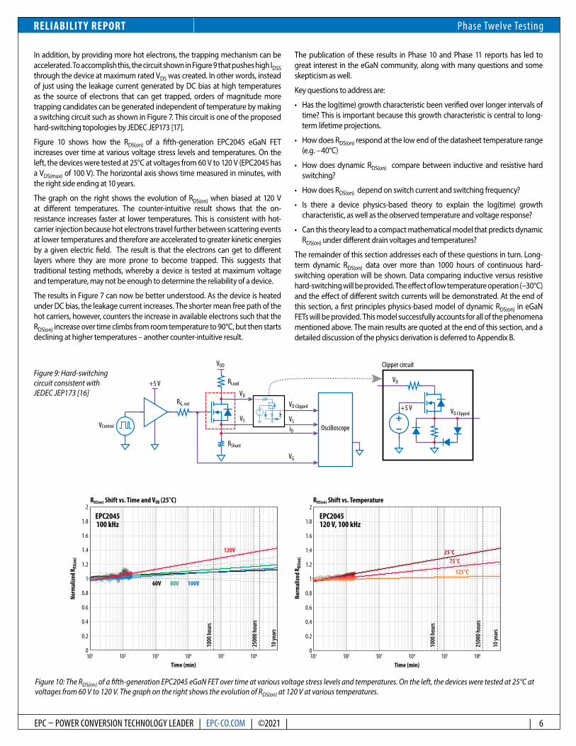
In addition, by providing more hot electrons, the trapping mechanism can be accelerated. To accomplish this, the circuit shown in Figure 9 that pushes high IDSS through the device at maximum rated VDS was created. In other words, instead of just using the leakage current generated by DC bias at high temperatures as the source of electrons that can get trapped, orders of magnitude more trapping candidates can be generated independent of temperature by making a switching circuit such as shown in Figure 7. This circuit is one of the proposed hard-switching topologies by JEDEC JEP173 [17].
Figure 10 shows how the RDS(on) of a fifth-generation EPC2045 eGaN FET increases over time at various voltage stress levels and temperatures. On the left, the devices were tested at 25°C at voltages from 60 V to 120 V (EPC2045 has a VDS(max) of 100 V). The horizontal axis shows time measured in minutes, with the right side ending at 10 years.
The graph on the right shows the evolution of RDS(on) when biased at 120 V at different temperatures. The counter-intuitive result shows that the on-resistance increases faster at lower temperatures. This is consistent with hot-carrier injection because hot electrons travel further between scattering events at lower temperatures and therefore are accelerated to greater kinetic energies by a given electric field. The result is that the electrons can get to different layers where they are more prone to become trapped. This suggests that traditional testing methods, whereby a device is tested at maximum voltage and temperature, may not be enough to determine the reliability of a device.
The results in Figure 7 can now be better understood. As the device is heated under DC bias, the leakage current increases. The shorter mean free path of the hot carriers, however, counters the increase in available electrons such that the RDS(on) increase over time climbs from room temperature to 90°C, but then starts declining at higher temperatures – another counter-intuitive result.
Clipper circuit
+5 V
+5 VRG, ext
RLoad
RShunt
VS VS
VD
VD
VG
iD
VD ClippedVD Clipped
VDD
VControl Oscilloscope
Figure 9: Hard-switching circuit consistent with JEDEC JEP173 [16]
Figure 10: The RDS(on) of a fifth-generation EPC2045 eGaN FET over time at various voltage stress levels and temperatures. On the left, the devices were tested at 25°C at voltages from 60 V to 120 V. The graph on the right shows the evolution of RDS(on) at 120 V at various temperatures.
Nor
mal
ized R
DS(o
n)
101 102 103 104 105 106
Time (min)
RDS(on) Shift vs. TemperatureRDS(on) Shift vs. Time and VIN (25°C)
1000
hour
s
2500
0 hou
rs
10 ye
ars
125°C
25°C75°C
2
1.8
1.6
1.4
1.2
1
0.8
0.6
0.4
0.2
0
1000
hour
s
2500
0 hou
rs
10 ye
ars
Nor
mal
ized R
DS(o
n)
101 102 103 104 105 106
Time (min)
2
1.8
1.6
1.4
1.2
1
0.8
0.6
0.4
0.2
0
120V
100V80V60V
EPC2045100 kHz
EPC2045120 V, 100 kHz
The publication of these results in Phase 10 and Phase 11 reports has led to great interest in the eGaN community, along with many questions and some skepticism as well.
Key questions to address are:
• Has the log(time) growth characteristic been verified over longer intervals of time? This is important because this growth characteristic is central to long-term lifetime projections.
• How does RDS(on) respond at the low end of the datasheet temperature range (e.g. −40°C)
• How does dynamic RDS(on) compare between inductive and resistive hard switching?
• How does RDS(on) depend on switch current and switching frequency?
• Is there a device physics-based theory to explain the log(time) growth characteristic, as well as the observed temperature and voltage response?
• Can this theory lead to a compact mathematical model that predicts dynamic RDS(on) under different drain voltages and temperatures?
The remainder of this section addresses each of these questions in turn. Long-term dynamic RDS(on) data over more than 1000 hours of continuous hard-switching operation will be shown. Data comparing inductive versus resistive hard-switching will be provided. The effect of low temperature operation (−30°C) and the effect of different switch currents will be demonstrated. At the end of this section, a first principles physics-based model of dynamic RDS(on) in eGaN FETs will be provided. This model successfully accounts for all of the phenomena mentioned above. The main results are quoted at the end of this section, and a detailed discussion of the physics derivation is deferred to Appendix B.

RELIABILIT Y REPORT Phase Twelve Testing
EPC – POWER CONVERSION TECHNOLOGY LEADER | EPC-CO.COM | ©2021 | | 7
2.1 Continuous Hard Switching Beyond 1000 HoursThe resistive hard-switching system was used to test six samples of EPC2218 eGaN FETs simultaneously for over 1000 hours of continuous operation. The purpose of this test is to show that the charge trapping mechanism responsible for a long-term increase of RDS(on) follows a log(time) trend. If this trend is maintained over the long-term, then data from the first few hours can be used to project the expected RDS(on) after 10 or 15 years. Figure 11 shows the normalized RDS(on) over time of all the samples under test, and Figure 12 shows the difference between the line fits using either the first five hours of data, or the full 1150 hours.
The main source of error in the five-hour line fits are small temperature changes in the ambient temperature. These (random) temperature fluctuations tend to cancel out as the length of the test increases. Nevertheless, the short duration and long duration tests agree to within 10% on the projected RDS(on) after 15 years. This lends credence to the idea that short-term data collects (over a few hours) can be used to accurately project long-term dynamic RDS(on) behavior.
Note that the RDS(on) values shown in Figures 11 and 12 were calculated from captured oscilloscope waveforms taken periodically over the entire duration of the test, as previously described in EPC’s Phase 10 report [10]. While this approach generates an immense amount of data, it also offers the opportunity to look back at the high-speed voltage waveforms at any point in time throughout the test.
Figure 13 shows such a waveform, taken after 1000 hours of continuous hard switching. Referring to this figure, the device is switched on at time t0, and RDS(on) is measured by averaging over the period from t2 to t3, which are 0.5 – 1.0 μs after the switching transition. The interval from t0 to t1 is excluded because it contains a spurious transient signal while the clipper circuit settles. Note from the waveform, however, that there is essentially no difference in the RDS(on) between 0.3 μs and 1.0 μs after the transition. This, and a host of other data, demonstrates that eGaN technology does not suffer from a short-term recovery effect
Figure 11: Long-term dynamic RDS(on) for six samples of EPC2218 eGaN FETs under continuous resistive hard-switching operation for over 1000 hours at ambient temperature and a bias of 100 V. The graph on the top shows RDS(on) versus Time, while the bottom graph shows RDS(on) normalized to its value after the first 10 minutes. Note that even over 1000 hours of operation, RDS(on) does not deviate from a simple log(time) growth dependence.
Figure 12: Comparison of log(time) fits to the RDS(on) data, where the dashed line represents the fit over the first 5 hours, while the solid line represent the fit over the full 1150 hours. Data for two samples of EPC2218 are shown. Note that the short-term fit has a similar projection to the long-term fit, with small random differences of ± 10% on the 15 year projection.
Figure 13: High time resolution oscilloscope waveform of the RDS(on) in the first 1−2 μs after a switch on transition. This waveform was taken on an EPC2218 after 1000 hours of continuous resistive hard-switching. Note that there is no evidence of the “fast dynamic RDS(on)” recovery seen in other GaN technologies.
(or “fast dynamic RDS(on)”) during the first microsecond after the switch. This fast effect, however, has been reported in different GaN HEMT technologies. In eGaN, dynamic RDS(on) manifests only as a slow, secular rise following a log(t) dependence.
Different clipper solutions with shorter reaction times may be used to capture RDS(on) within less than 500 ns of turn-on. For instance, in [27] RDS(on) was captured after 50ns of turn-on for the same product, EPC2045, using a Double Pulse Test circuit. No “fast dynamic RDS(on),” was reported under inductive hard switching at 100 V and 20 A.
0.010
0.009
0.008
0.007
0.006
0.005
0.004
0.003
0.002
0.001
010-1 100 101 102
Time (hours)
R DS(o
n) (Ω
)
103 104 105
2.0
1.8
1.6
1.4
1.2
1.0
0.8
0.6
0.4
0.2
010-1 100 101 102
Time (hours)
Norm
alize
d R DS
(on)
103 104 105
Completed 1150 hours of continuous, uninterrupted operation
Completed 1150 hours of continuous, uninterrupted operation
15 ye
ars
15 ye
ars
0.010
0.009
0.008
0.007
0.006
0.005
0.004
0.003
0.002
0.001
0
0.010
0.009
0.008
0.007
0.006
0.005
0.004
0.003
0.002
0.001
0
10-1 100 101 102
Time (hours)
R DS(o
n) (Ω
)R DS
(on)
(Ω)
103 104 105
10-1 100 101 102
Time (hours)103 104 105
Projection calculated from data t ε [0.1,5] hours
Projection calculated from data t ε [0.1,5] hours
Sample 1
Sample 2
Projection calculated from data t ε [0.1,1150] hours
Projection calculated from data t ε [0.1,1150] hours
15 ye
ars
15 ye
ars
0 0.2 0.4 0.6 0.8 1 1.2 1.4 1.6 1.8 2-2
0
2
4
6
8
10
12
-1
0
1
2
3
4
5
6
Time (μs)t0 t1 t2 t3
R DS(o
n) (m
Ω)
V GS (V
)
Gate to Source voltage, VGS
On-resistance, RDS(on)
t0 DUT turn-on
t0 → t1Clipper circuit reaction time
t2 → t3
Average window for long term plots

RELIABILIT Y REPORT Phase Twelve Testing
EPC – POWER CONVERSION TECHNOLOGY LEADER | EPC-CO.COM | ©2021 | | 8
2.2 Inductive vs. Resistive Hard Switching and the Effect of Switch CurrentSeveral customers have raised concerns that resistive hard switching is not truly representative of the kind of hot-carrier stress that occurs during inductive hard switching. These concerns have also been voiced in the academic literature, at conference proceedings, and by other GaN manufacturers. The argument centers on the loci in current-voltage space the part traverses during an on-transition. For an inductive transition, the FET experiences higher current during the critical interval of time when both voltage and current are high, precisely the conditions that lead to hot-carrier effects. Though plausible, these arguments are mostly hand-waving, and are never supported by hard data or solid theory.
To address this question, EPC developed a custom test fixture to measure both inductive and resistive hard switching. A key feature of this system is the ability to alternate from inductive to resistive modes (and back) on the same device under test. For inductive mode, the test circuit is a boost converter operating in Continuous Conduction Mode (CCM). In both modes, the part is switching continuously at 200 kHz, and oscilloscope traces are captured periodically, allowing us to monitor both short term and long term dynamic RDS(on).
Figure 14 shows data for an EPC2204 eGaN FET switching at 80 V. For the first four hours, the part was operated in inductive mode. After that, it was operated in resistive mode for the ensuing four hours. To guarantee a fair comparison, the off-state voltage across the device, frequency, duty cycle, and current at turn-on were kept the same for the resistive and inductive cases. As can be seen in the figure, there is no discernable difference in the slope or intercept of the log(t) growth characteristic: resistive and inductive hard-switching are essentially indistinguishable in terms of dynamic RDS(on). The same is true of short-term effects within the first microsecond of the transition; for neither mode displayed any “fast” recovery effects.
This surprising result implies that the mechanism responsible for RDS(on) shifts in eGaN FETs is either independent or weakly dependent on the detailed loci of current-voltage traversed during a transition. In both switching cases, there is simultaneous voltage and current during turn-on. While in resistive switching, the voltage across the transistor decreases as the current rises; whereas, in a purely inductive turn-on, the current rises before the voltage collapses. The fact that dynamic RDS(on) is so similar between the modes suggests that the electron current has a weak influence on hot-carrier trapping.
To explore this hypothesis more, resistive hard-switching measurements on an EPC2206 device at two different switch currents was conducted. Figure 15 (top) shows the results. One part was tested at 12.8 A and another was tested at 25.6 A,
double the switch current. To account for the distinct device heating in each case, RDS(on) is normalized to its value at 10 minutes. Here, as before, a surprising result is obtained – the switching current has no discernible effect on either the slope or intercept of the log(t) growth characteristic. Similarly, the effect of switch current on the slope was also evaluated under inductive hard-switching.
Figure 15 (bottom) shows the same EPC2204 device operated in a boost converter under inductive hard switching at different currents and 80 V output voltage. Starting with 1 A switch current for the first 1.5 hours, followed 3.5 hours with 5 A, and finishing with 10 A for 20 additional hours. For an easier interpretation of the results, the RDS(on) measurements were normalized to the thermal steady state RDS(on) at the beginning of each interval.
As discussed below, EPC’s physics-based model of dynamic RDS(on) explains the results above. This model predicts that switch current (or the switching loci) has no impact on slope of the log(t) growth line, as observed. Furthermore, the model predicts that switch current does affect the intercept of the line, but only weakly. In fact, the intercept (or additive vertical offset) of the line will increase like the logarithm of the switch current. For the same reason, the fine details of the switching loci have almost no impact, and inductive and resistive hard switching are equally valid methods to characterize dynamic RDS(on).
While equally valid to an inductive test circuit, a resistive circuit presents several practical advantages when it comes to evaluating dynamic RDS(on). For one, the circuit is simpler and more compact, allowing it to be integrated on probe cards for wafer-level characterization. For another, the lack of voltage overshoot during turn off allows for testing at voltages closer to the breakdown voltage, achieving operating points in the switching loci even more severe than possible with an inductive switching circuit. For these reasons, EPC will continue using a resistive switching circuit as the primary method for device characterization.
Figure 14: Comparison of inductive versus resistive hard switching on an EPC2204 FET switching at 80 V, 200 kHz. The same part was tested under inductive mode for the first four hours, followed by resistive mode for the next four hours. Both modes are essentially indistinguishable in terms of dynamic RDS(on).
Figure 15: Effect of switch current on dynamic RDS(on). (top) Two EPC2206 devices were tested under resistive hard switching at 64 V, 200 kHz. (bottom) The same device was tested under inductive hard switching and three different currents at 80 V, 200 kHz. No discernible difference was found in the slope or intercept of the log(t) growth characteristics.
2.0
1.8
1.6
1.4
1.2
1.0
0.8
0.6
0.4
0.2
0100 102
Time (min.)
EPC2204 under Hard Switching at 80 V, 3.2 A, 200 kHz
Norm
alize
d R DS
(on)
104 106
Resistive
Inductive
15 ye
ars
Norm
alize
d R DS
(on)
2.0
1.8
1.6
1.4
1.2
1.0
0.8
0.6
0.4
0.2
0101 102
Time (hours)103 104 105 106
Norm
alize
d R DS
(on)
2.0
1.8
1.6
1.4
1.2
1.0
0.8
0.6
0.4
0.2
0101 102
Time (hours)
EPC2206 under Resistance Hard Switching at 64 V, 200 kHz
EPC2204 under Resistance Hard Switching at 80 V, 200 kHz
103 104 105 106
15 ye
ars
15 ye
ars
12.5 A
5 A 10 A1 A
25 A

RELIABILIT Y REPORT Phase Twelve Testing
EPC – POWER CONVERSION TECHNOLOGY LEADER | EPC-CO.COM | ©2021 | | 9
2.3 Alternating Hot/Cold Switching TestEPC has performed additional hard-switching reliability tests at lower temperatures than reported previously [10]. Using a specially designed thermoelectric module attached to the backside (case) of the device under test, it was possible to achieve temperatures as low as −30°C while the part is switching. (Note that this condition is academic in nature; even in very cold ambient conditions, the device would not stay at this low temperature owing to self-heating).
A typical result is shown in Figure 16, where an EPC2059 device was operated under continuous hard switching while the case temperature was modulated between 80°C and −30°C for two complete cycles. As can be seen, when the temperature drops to −30°C, RDS(on) drops as well, owing to increased channel mobility. However, it begins to rise in time following a log(t) growth characteris-tic with a distinctly higher slope than it had at 80°C. As the temperature is cycled again, RDS(on) ratchets back and forth between these two distinct lines.
This data provides even more evidence that the slope of the log(t) growth law has a negative temperature coefficient, which is explained in the model to follow. Though the slope is indeed higher at −30°C (close to datasheet minimum of −40°C), even if the part were operated non-stop for 10 years in this unrealistic condition, RDS(on) would still be lower than had it operated at 80°C for the same time.
Figure 16: Effect of alternating hot-cold conditions on dynamic RDS(on) for an EPC2059. (Top) Case temperature versus Time, as controlled by a thermoelectric cooler. (Bottom) RDS(on) versus Time. Switching is continuous throughout at 100 V and 100 kHz.
R DS(o
n) (Ω
) T Ca
se (°C
)
80
40
0
-40
0.015
0.01
0.005
0101100 102
Time (hours)103 104 105 106
15 ye
ars
10 ye
ars
80°C
-30°C
100 kHz, 80°C
100 kHz, -30°C
2.4 Physics-Based Dynamic RDS(on) and Lifetime ModelsEPC has developed a first-principles mathematical model to describe the dynamic RDS(on) effect in eGaN FETs from the basic physics of hot carrier scattering into surface traps. The model successfully predicts all of the following phenomena:
• RDS(on) grows with time as log(t)
• The slope of RDS(on) over time has a negative temperature coefficient (i.e., lower slope at higher temperature)
• Switching frequency does not affect the slope, but causes a small vertical offset
• Switching current does not affect the slope, but causes a small vertical offset
• Negligible difference between inductive and resistive hard switching
In this section, the model equations are summarized without explanation. The theoretical derivation of these equations appears in Appendix B.
2.4.1 Normalized RDS(on) Shift EquationEquation 2 models RDS(on) as a function of time, temperature, and drain voltage. It involves five device-dependent parameters. The values of the parameters listed in the table below are appropriate for an EPC2045 or other 100 V, 5th Generation, FETs listed in Appendix B. Natural log (base e) was used for fitting. While the general form of this equation applies to all eGaN FETs, please consult EPC for parameter values specific to other eGaN products.
Independent Variables:
VDS = Drain voltage (V)T = Device temperature (K)t = Time (min)
Parameters:
a = 0.00 (unitless)b = 2.0E-5 (K-1/2)ћωL0 = 92 meVVFD = 100 V (appropriate for Gen5 100 V products only)α = 10 (V)
2.4.2 Switching Frequency/Current Scaling Relation Equation 3 allows users to quantify the effect of changing switching frequency (f) or switching current (I) from one set of conditions (f1,I1) to another set (f2,I2). The effect of these changes on RDS(on) is merely a vertical offset in the log(t) growth characteristic from one condition to the other. The slope of the characteristic does not change, only the vertical offset does. Note that this offset is dependent on the logarithm of the frequency or current and is therefore weakly influenced by these variables.
2.4.3 Hard-Switching Lifetime Model Equation 4 models the expected lifetime of an eGaN FET based on operating conditions of drain voltage and temperature. This equation is useful for customers needing lifetime estimates under specific mission profiles to fulfill certain quality or reliability requirements. It is derived in a straightforward way from Equation 2 by solving for the time at which RDS(on) increases by 20%. It can be readily adapted to other definitions of lifetime.
log 1 exp √ exp log
⟨ ⟩ exp .
√ (min)
; , ; , log log
Eq. 2
Eq. 4
Eq. 3
RELIABILIT Y REPORT Phase Twelve Testing
EPC – POWER CONVERSION TECHNOLOGY LEADER | EPC-CO.COM | ©2021 | | 10
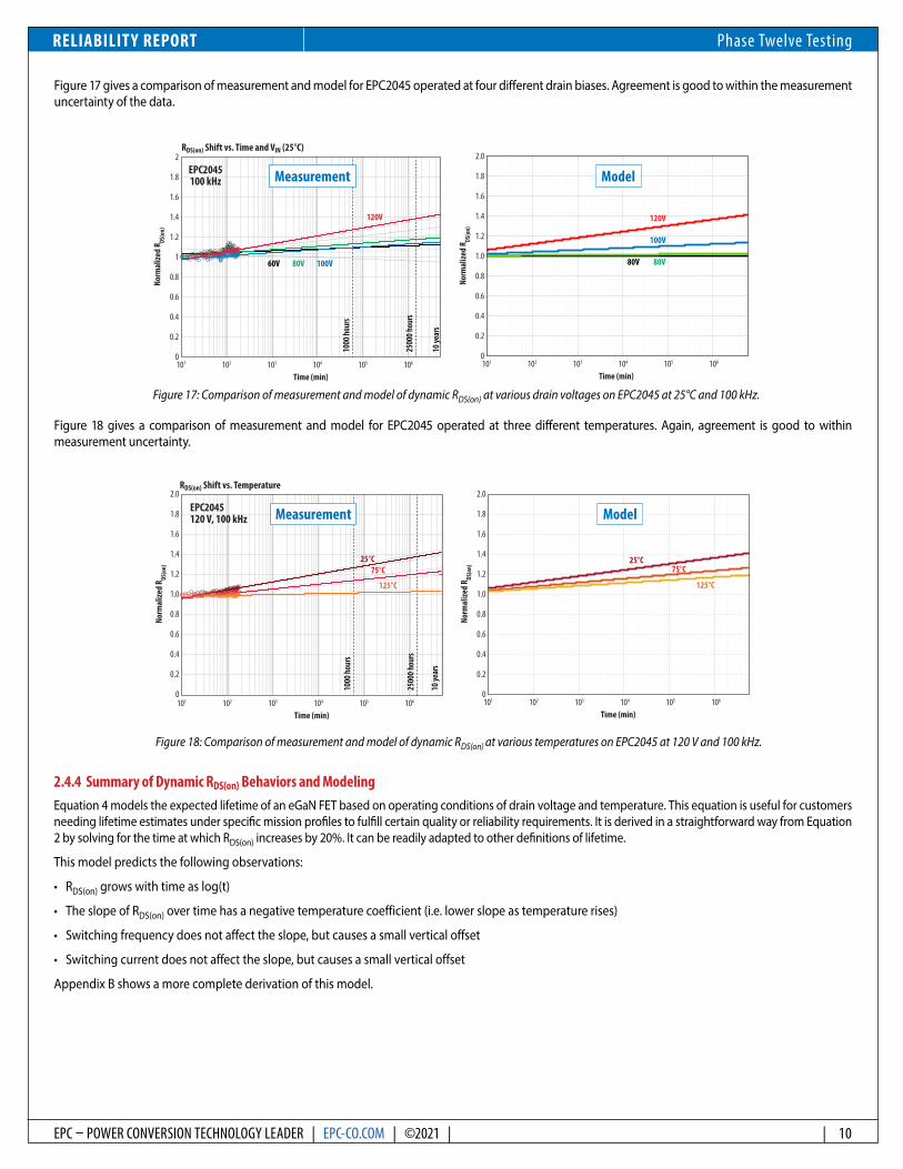
Figure 17 gives a comparison of measurement and model for EPC2045 operated at four different drain biases. Agreement is good to within the measurement uncertainty of the data.
Figure 18 gives a comparison of measurement and model for EPC2045 operated at three different temperatures. Again, agreement is good to within measurement uncertainty.
Nor
mal
ized
R DS(o
n)
101 102 103 104 105 106
Time (min)
2.0
1.8
1.6
1.4
1.2
1.0
0.8
0.6
0.4
0.2
0
120V
100V
80V80V
RDS(on) Shift vs. Time and VIN (25°C)
1000
hou
rs
2500
0 hou
rs
10 ye
ars
Nor
mal
ized
R DS(o
n)
101 102 103 104 105 106
Time (min)
2
1.8
1.6
1.4
1.2
1
0.8
0.6
0.4
0.2
0
120V
100V80V60V
EPC2045100 kHz Measurement Model
Nor
mal
ized
R DS(o
n)
101 102 103 104 105 106
Time (min)
RDS(on) Shift vs. Temperature
1000
hou
rs
2500
0 hou
rs
10 ye
ars
25°C75°C 75°C
EPC2045120 V, 100 kHz
Nor
mal
ized
R DS(o
n)
101 102 103 104 105 106
Time (min)
2.0
1.8
1.6
1.4
1.2
1.0
0.8
0.6
0.4
0.2
0
2.0
1.8
1.6
1.4
1.2
1.0
0.8
0.6
0.4
0.2
0
Measurement Model
125°C 125°C
25°C
Figure 17: Comparison of measurement and model of dynamic RDS(on) at various drain voltages on EPC2045 at 25°C and 100 kHz.
Figure 18: Comparison of measurement and model of dynamic RDS(on) at various temperatures on EPC2045 at 120 V and 100 kHz.
2.4.4 Summary of Dynamic RDS(on) Behaviors and Modeling Equation 4 models the expected lifetime of an eGaN FET based on operating conditions of drain voltage and temperature. This equation is useful for customers needing lifetime estimates under specific mission profiles to fulfill certain quality or reliability requirements. It is derived in a straightforward way from Equation 2 by solving for the time at which RDS(on) increases by 20%. It can be readily adapted to other definitions of lifetime.
This model predicts the following observations:
• RDS(on) grows with time as log(t)
• The slope of RDS(on) over time has a negative temperature coefficient (i.e. lower slope as temperature rises)
• Switching frequency does not affect the slope, but causes a small vertical offset
• Switching current does not affect the slope, but causes a small vertical offset
Appendix B shows a more complete derivation of this model.

RELIABILIT Y REPORT Phase Twelve Testing
EPC – POWER CONVERSION TECHNOLOGY LEADER | EPC-CO.COM | ©2021 | | 11
Figure 19: EPC2034C SOA plot. The “Limited by RDS(on)” line is based on data sheet maximum specification for RDS(on) at 150°C. Measurements for 1 ms (purple triangles) and 100 µs (green dots) pulses are shown together. Failures are denoted by red triangles (1 ms) or red dot (100 µs). Note that all failures occur outside the data sheet SOA region.
100
10
1
0.10.1 1
Limited by RDS(on)
100 μs pulse (pass)100 μs pulse (fail)1 ms pulse (pass)
1 ms pulse (fail)
10VDS - Drain-Source Voltage (V)
EPC2034C 200 V
100
I D - Dra
in Cu
rrent
(A)
SECTION 3: SAFE OPERATING AREA Safe operating area (SOA) testing exposes the eGaN FET to simultaneous high current (ID) and high voltage (VDS) for a specified pulse duration. The primary purpose is to verify the FET can be operated without failure at every point (ID, VDS) within the datasheet SOA graph. It is also used to probe the safety margins by testing to fail outside the safe zone.
During SOA tests, the high-power dissipation within the die leads to a rapid rise in junction temperature and the formation of strong thermal gradients. For sufficiently high power or pulse duration, the device simply overheats and fails catastrophically. This is known as thermal overload failure.
In Si MOSFETs, another failure mechanism known as secondary breakdown (or Spirito effect [14]) has been observed in SOA testing. This failure mode, which occurs at high VD and low ID, is caused by an unstable feedback between junction temperature and threshold VTH. As the junction temperature rises during a pulse, VTH drops, which can cause pulse current to rise. The rising current, in turn, causes temperature to rise faster, thereby completing a positive feedback loop that leads to thermal runaway and ultimate failure. A goal of this study is to determine if the Spirito effect exists in eGaN FETs.
EPC designed and built a custom Safe Operating Area test system for eGaN FETs. The system is described in detail in Appendix D. In brief, the circuit works similar to a curve tracer. The gate bias on the device under test (DUT) is set before the pulse and is used to modulate the ultimate pulse current. The drain voltage is then pulsed onto the drain by means of a p-channel control FET for a specified pulse duration.
For DC, or long-duration pulses, the SOA capability of the FET is highly dependent on the heatsinking of the device. This can present a huge technical challenge to assess the true SOA capability, often requiring specialty water-cooled heatsinks. However, for short pulses (< 1 ms), the heatsinking does not impact SOA performance. This is because on short timescales, the heat generated in the junction does not have sufficient time to diffuse to any external heatsink. Instead, all of the electrical power is converted to raising the temperature (thermal capacitance) of the GaN film and nearby silicon substrate. As a result of these considerations, SOA tests were conducted at two pulse durations: 1 ms and 100 µs.
Figure 19 shows the SOA data of 200 V EPC2034C. In this plot, individual pulse tests are represented by points in (ID, VDS) space. These points are overlaid on the datasheet SOA graph. Data for both 100 µs and 1 ms pulses data are shown together. Green dots correspond to 100 µs pulses in which a part passed, whereas red dots indicate where a part failed. A broad area of the SOA was interrogated without any failures (all green dots), ranging from low VDS all the way to VDS(max) (200 V). All failures (red dots) occurred outside the SOA, indicated by the green line in the datasheet graph. The same applies to 1 ms pulse data (purple and red triangles); all failures occurred outside of the datasheet SOA.

RELIABILIT Y REPORT Phase Twelve Testing
EPC – POWER CONVERSION TECHNOLOGY LEADER | EPC-CO.COM | ©2021 | | 12
Figure 20: SOA results for EPC2045, EPC2212, EPC2014C. Measurements for 1 ms (purple triangles) and 100 µs (green dots) pulses are shown together. Failures are denoted by red triangles (1 ms) or red dot (100 µs). Note that for all parts, all failures occur outside the data sheet SOA region.
100
10
1
0.1
100
10
1
0.1
100 μs pulse (pass)100 μs pulse (fail)1 ms pulse (pass)
1 ms pulse (fail)
100 μs pulse (pass)100 μs pulse (fail)1 ms pulse (pass)
1 ms pulse (fail)
100 μs pulse (pass)100 μs pulse (fail)1 ms pulse (pass)
1 ms pulse (fail)
EPC2045 100 V
EPC2212 100 V AEC
I D - Dra
in Cu
rrent
(A)
I D - Dra
in Cu
rrent
(A)
I D - Dra
in Cu
rrent
(A)
0.1 1 10VDS - Drain-Source Voltage (V)
100
0.1 1 10VDS - Drain-Source Voltage (V)
100
100
10
1
0.1
EPC2014C 40 V
0.1 1 10VDS - Drain-Source Voltage (V)
100
Limited by RDS(on)
Limited by RDS(on)
Limited by RDS(on)
Figure 20 provides SOA data for three more parts, AEC EPC2212 (4th generation automotive 100 V), EPC2045 (5th generation 100 V), and EPC2014C (4th generation 40 V). In all cases, the datasheet safe operating area has been interrogated without failures, and all failures occur outside of SOA limits, often well outside the limits.
The datasheet SOA graph is generated with finite element analysis, using a thermal model of the device including all relevant layers along with their heat conductivity and heat capacity. Based on transient simulations, the SOA limits are determined by a simple criterion: for a given pulse duration, the power dissipation must be such that the junction temperature does not exceed 150°C before the end of the pulse. This criterion results in limits based on constant power, denoted by the 45° green (100 µs) and purple (1 ms) lines in the SOA graph. This approach leads to a datasheet graph that defines a conservative safe operating zone, as evidenced by the extensive test data in this study. In power MOSFETs, the same constant power approach leads to an over-estimate of capability in the high voltage regime, where failure occurs prematurely due to thermal instability (Spirito effect).
However, from the perspective of the physics of failure, it is evident from Figure 20 that in certain cases the eGaN FETs can survive well outside of the nominal safe zone, but the operating margin decreases at higher drain-source bias and longer pulse durations. To gain deeper knowledge of the mechanisms at play, EPC plans to conduct further test-to-fail studies at higher VDS (beyond datasheet maximum) and longer pulse durations. These studies will require the addition of device heatsinking to get meaningful results. The measurement technology is continuing to be refined and failed devices are being dissected to look for intrinsic failure mechanisms.
While the exact physics of failure may still be unknown, the main outcome of this study is clear − eGaN FETs will not fail when operated within their datasheet SOA.

RELIABILIT Y REPORT Phase Twelve Testing
EPC – POWER CONVERSION TECHNOLOGY LEADER | EPC-CO.COM | ©2021 | | 13
Figure 21: EPC2203 fault under load test waveforms for a series of increasing drain voltages. Drain pulse is 10 µs and VGS = 6 V. The device did not fail for this pulse width. (top) VDS vs. time. VDS is Kelvin sensed directly at the device terminals. (bottom) IDS vs. time. Note that IDS decreases over time due to self-heating. (middle) Resulting output curve for this test sequence. Drain current is reported as the average current during the pulse. Drain current rolls over in the saturation region owing to device heating at higher VDS.
70
60
50
40
30
20
10
0
100
80
60
40
20
0
60
50
40
30
20
10
0
0 5 10 15 20 25
Drain-Source Voltage Pulses
Drain Current Pulses
Output I-V of EPC2203
Drai
n-So
urce
Volta
ge (V
)Dr
ain
Curre
nt (A
)Dr
ain
Curre
nt (A
)
Time (μs)
0 5 10 15 20 25Time (μs)
10-1 100 101 102
Drain-Source Voltage (V)
SECTION 4: SHORT CIRCUIT ROBUSTNESS TESTING Short-circuit robustness refers to the ability of a FET to withstand uninten-tional fault conditions that may occur in a power converter while in the ON (conducting) state. In such an event, the part will experience the full bus voltage combined with a current that is limited only by the inherent saturation current of the transistor and the circuit parasitic resistance, which varies with the application and location of the fault. If the short-circuit state is not quenched by protection circuitry, the extreme power dissipation will ultimately lead to thermal failure of the FET. The goal of short-circuit testing is to quantify the “withstand time” the part can survive under these conditions. Typical protection circuits (e.g. de-saturation protection for IGBT gate drivers) can detect and react to over-current conditions in 2-3 µs. It is therefore desirable if the eGaN FET can withstand unclamped short-circuit conditions for about 5 µs or longer.
The two main test circuits used for short-circuit robustness evaluation are [18]:
• Hard-switched fault (HSF): gate is switched ON (and OFF) with drain voltage applied
• Fault under load (FUL): drain voltage is switched ON while gate is ON
For this study, EPC tested parts in both fault modes and found no significant differences in the withstand time. Therefore, the focus will be on FUL results for the remainder of this discussion. However, it is important to note that from HSF testing, eGaN FETs did not exhibit any latching or loss of gate control that can occur in silicon-based IGBTs [18]. This result was expected given the lack of parasitic bipolar structures with the eGaN devices. Until the time the FETs fail catastrophically, the short-circuit can be fully quenched by switching the gate LOW, an advantageous feature for protection circuitry design. Full details of the test methodology are provided in Appendix D.
Two representative eGaN FETs were tested:
1. EPC2203 (80 V): 4th generation automotive grade (AEC) device
2. EPC2051 (100 V): 5th generation device
These devices were chosen because they are the smallest in their product families. This simplified the testing owing to the high currents required for short-circuit evaluation. However, based on simple thermal scaling arguments, the withstand time is expected to be identical for other in-family devices. EPC2203 results cover EPC2202, EPC2206, EPC2201 and EPC2212; EPC2051 covers EPC2045 and EPC2053.
Figure 21 shows fault under load data on EPC2203 for a series of increasing drain voltages. With VGS at 6 V (the data sheet max), and a 10 µs drain pulse, the device did not fail all the way up to VDS of 60 V. Under these conditions, over 3 kW is dissipated in a 0.9 mm x 0.9 mm die. At the higher VDS, the current is seen to decay over time during the pulse. This is a result of rising junction temperature within the device and does not signify any permanent degradation.

RELIABILIT Y REPORT Phase Twelve Testing
EPC – POWER CONVERSION TECHNOLOGY LEADER | EPC-CO.COM | ©2021 | | 14
The lower rows in Table 2 provide pulse power and energy relative to die size. To gain insight into the relationship between these quantities and the time to failure, time-dependent heat transfer was simulated to determine the rise in junction temperature ΔTJ during the short-circuit pulse. The results are shown in Figure 23.
Using a longer pulse duration (25 µs), the parts eventually fail from thermal overload. Representative waveforms are shown in Figure 22. The time of failure is marked by the abrupt rise in drain current. After this event, the devices are permanently damaged. The withstand time is measured from the beginning of the pulse to the time of failure.
To gather statistics on the withstand time, cohorts of eight parts were tested to failure using this approach. Table 2 summarizes the results. EPC2203 was tested at both 5 V (recommended gate drive) and 6 V (VGS(max)), with mean withstand time of 20 µs and 13 µs respectively. Note that the part survives less time at 6 V because of the higher saturation current. EPC2051 exhibited a slightly lower time-to-fail (9.3 µs) compared with the EPC2203 at 6 V. This is expected because of the more aggressive scaling and current density of 5th generation products. However, in all cases, the withstand time is comfortably long enough for most short-circuit protection circuits to respond and prevent device failure. Furthermore, the withstand time showed small part-to-part variability.
100
80
60
40
20
0
200
150
100
50
0
200
150
100
50
0
100
80
60
40
20
0
0 5 10 15 20 25 30
Unclamped Short-Circuit EPC2203
Unclamped Short-Circuit EPC2051
Drai
n-So
urce
Volta
ge (V
)
Drai
n Cu
rrent
(A)
Drai
n Cu
rrent
(A)
Drai
n-So
urce
Volta
ge (V
)
Time (μs)
0 5 10 15 20 25 30Time (μs)
Figure 22: Fault under load test waveforms for a typical EPC2203 (top) and EPC2051 (bottom) at VDS = 60 V, VGS = 6 V and a 25 µs drain pulse. The abrupt rise in drain current marks the time of catastrophic thermal failure.
Short-circuit pulseVDS = 60 V
EPC2203 (Gen 4) EPC2051 (Gen 5)VGS = 6 V VGS = 5 V VGS = 6 V VGS = 5 V
Mean TTF (μs) 13.1 20.0 9.33 21.87Std. dev. (μs) 0.78 0.37 0.21 2.95Min. TTF (μs) 12.1 19.6 9.08 18.53Avg pulse power (kW) 3.211 2.554 5.516 3.699Energy (mJ) 43.36 50.24 50.43 77.34Die area (mm2) 0.9025 1.105Avg power/area (kW/mm2) 3.558 2.830 4.99 3.35Energy/area (mJ/mm2) 48.05 55.67 45.64 69.99
Table 2: Short-circuit withstand time statistics for EPC2203 and EPC2051. Statistics derived from eight parts in each condition. Withstand times are tightly distributed around mean value. Average pulse power and energy correspond to a typical part within the population.
1200
1000
800
600
400
200
00 5 10 15 20 25
ΔTJ = k · P · t 1/2
EPC2051 (6 V)
Short-circuit Time (μs)
Junc
tion T
empe
ratu
re Ri
se (°
C)
EPC2203 (6 V)
EPC2051 (5 V)
EPC2203 (5 V)
Figure 23: Simulated junction temperature rise vs time during the short-circuit pulses for both EPC2051 and EPC2203 at both 5 V and 6 VGS. Measured failure times are indicated by red markers. Note that EPC2203 fails catastrophically at a ΔTJ of around 850°C, whereas EPC2051 fails around 1050°C. The simulated ΔTJ is well fit by a simple square root dependence on time (heat diffusion), as shown in the equation. P denotes the average power per unit area, and k = 6.73 x 10⁻⁵ K/W s1/2.
The intense power density during the pulse leads to rapid heating in the GaN layer and nearby silicon substrate. Because the pulse is short and heat transfer is relatively slow, only a small thickness of semiconductor (<~100 µm in depth) can help to absorb the energy. The temperature grows as the square root of time (characteristic of heat diffusion), and linearly with the pulse power. As can be seen in Figure 23, for EPC2203, both the 5 V and 6 V conditions fail at the same junction temperature rise of ~850°C. The same is true for EPC2051, where both conditions fail at the same ΔTJ of ~1050°C. Three important conclusions stem from these results:
1. For a given device, the time to failure is inversely proportional to the power dissipation squared (P-2). This applies for short-circuit and SOA pulses of duration < ~1 ms.
2. The intrinsic failure mode resulting from high power pulses is directly linked to the junction temperature exceeding a certain critical value.
3. Wide bandgap eGaN devices can survive junction temperatures (> 800 °C) that are totally inaccessible to silicon devices owing to free-carrier thermal runaway.
Further analysis is required to determine the exact mechanism of failure. Nonetheless, the experimental results presented in this study demonstrate the outstanding short-circuit capability of eGaN FETs, allowing users to design their systems and short-circuit protection schemes with ample safety margins.

RELIABILIT Y REPORT Phase Twelve Testing
EPC – POWER CONVERSION TECHNOLOGY LEADER | EPC-CO.COM | ©2021 | | 15
SECTION 5: SHORT CURRENT PULSE RELIABILITY (LIDAR APPLICATION)eGaN FETs are widely adopted in lidar circuits for autonomous vehicles, where they offer several key benefits:
• Faster switching for shorter pulses and better range resolution
• Smaller footprint which enables high power density, low inductance and compact solutions
• Higher efficiency at higher pulse repetition rate
In a lidar application, the GaN device experiences short high current pulses, on the order of 1−5 ns, which drive a laser diode to generate narrow optical pulses [19]. The peak currents are usually substantially greater than 50% of the FET pulse current rating. The pulse duty cycle is typically low, and the pulse repetition frequency (PRF) is in the range of 10 to 100 kHz. When not being pulsed, the part is in the OFF state, exposed to a certain drain bias.
This stress condition is somewhat unusual for a power device, making it difficult to predict lifetime in operation by projecting conventional DC reliability tests such as HTGB or HTRB. Even GaN-specific tests, like the hard-switching reliability testing discussed in Section 2, do not effectively emulate the stress conditions in a lidar circuit. From the standpoint of physics of failure, the simultaneous high current and voltage during a pulse raises concerns about hot-carrier effects, potentially leading to VTH or RDS(on) shifting within the device. In addition, the cumulative effect of repetitive high current pulses raises the specter of electro-migration leading to degradation of the solder joints.
To address these concerns in this developing market, EPC initiated a novel test method in collaboration with key lidar customers. This lidar reliability testing is part of EPC’s Beyond AEC Initiative [20], a series of GaN specific stress tests that go beyond the conventional reliability tests developed for MOSFETs as part of AEC-Q101 standard.
5.1 Long-Term Stability Under High Current PulsesThe concept is to stress parts in an actual lidar circuit for a total number of pulses commensurate with their ultimate mission profile. The mission profiles for automotive lidar vary from customer to customer. A typical automotive profile would call for a 15-year life, with two hours operation per day, at 100 kHz pulse repetition frequency (PRF). This corresponds to approximately four trillion total lidar pulses. Some worst-case scenarios might call for 10−12 trillion pulses in service life. By testing a population of devices to the end of their full mission profile, this test method directly demonstrates the lifetime of eGaN devices in a lidar mission. Note that this direct approach obviates the need for an acceleration factor or activation energy of dubious validity. It also removes the need to somehow project lifetime estimates from standard reliability tests to the unique stress conditions of lidar.
Figure 25: Long-term stability of RDS(on) and VTH during lidar reliability testing. These parameters are measured at six-hour intervals on every part by briefly interrupting the lidar stress. Note that VTH is inferred by measuring RDS(on) at a series of gate voltages. Data for four EPC2202 (red) devices and four EPC2212 (blue) devices are overlaid in the plots. Note the excellent stability of these key parameters over total number of pulses corresponding to a typical automotive lifetime.
Drain voltage
Gate voltage
Current
100
80
60
40
20
0
3
2
1
0
0 2 4 6 8 10 12 14
0 2 4 6 8 10 12 14
Pulses
Pulses
Peak
Curre
nt (A
)Pu
lse W
idth
(ns)
x 1012
x 1012
EPC2202
EPC2212
AEC-Q101 series of discrete FETs
8 samples (>7000h)
0 failures and perfect pulse stability
13 Tr
illio
n13
Trill
ion
EPC2202
EPC2212
EPC2202
EPC2212
0.025
0.020
0.015
0.010
0.005
00 2 4 6 8 10 12
0 2 4 6 8 10 12
Pulses
Pulses
R DS(o
n) (Ω
)
5
4
3
2
1
0
V TH (V
)
EPC2212
EPC2202
EPC2212
EPC2202
5.2 Test Methodology and ResultsTo achieve the large number of pulses, parts are stressed continuously at a PRF much higher than in typical Lidar circuits. The test circuit is based on EPC’s popular EPC9126 lidar application board. Experimental details are provided in Appendix C. For this study, two popular AEC grade parts were put under test: EPC2202 (80 V) and EPC2212 (100 V). Four parts of each type were tested simultaneously. During the stress, two key parameters are continuously monitored on every device: (i) peak pulse current and (ii) pulse width. These parameters are both critical to the range and resolution of the lidar system.
Figure 24 shows the results over the first 4.2 trillion pulses. The cumulative number of pulses corresponds to a typical automotive lifetime. While this is an indirect monitor of the health of the eGaN device, it indicates that no degradation mechanisms have occurred that would adversely impact circuit performance.
Figure 24: Long-term stability of pulse with (bottom right) and pulse height (top right) over 4.2 trillion lidar pulses. Data for four EPC2202 (red) devices and four EPC2212 (blue) devices are overlaid in the plots. Note the excellent stability of these key parameters over total number of pulses corresponding to a typical automotive lifetime. Oscilloscope image of pulses in upper left.

RELIABILIT Y REPORT Phase Twelve Testing
EPC – POWER CONVERSION TECHNOLOGY LEADER | EPC-CO.COM | ©2021 | | 16
6.2 Backside Pressure Test Another critical aspect of the mechanical robustness of eGaN devices is how well they handle backside pressure. This is an important consideration for applications that require backside heatsinking to the die. It is also important to determine the safe “pick-and-place” place force during assembly.
EPC performed backside pressure tests up to 400 psi, where the pressure is calculated by the force applied divided by the die area. Figure 27 shows the laboratory pressure tester that was employed. The pressure was applied directly to the backside of the die using a loading speed of 0.6 mm/min. Before and after the pressure test, parametric testing was performed to determine pass or fail. Subsequently, the parts were exposed to humidity-bias testing (H3TRB) at 60 VDS, 85°C, and 85% relative humidity for 300 hours. H3TRB is effective to determine if there were any latent failures caused by mechanical damage (internal cracking) from the pressure test.
EPC2212 (100 V, LGA) and EPC2034C (200 V, BGA) were tested and both passed 400 psi. The data is included in Table 3. These results show that eGaN FETs have enough margin to handle backside pressure that is normally used at a PCB assembly house. Though these parts survived 400 psi, EPC recommends limiting maximum backside pressure to 50 psi or less.
1.0E+05
1.0E+04
1.0E+03
1.0E+02
Die S
hear
Stre
ngth
(Gra
ms)
EPC2203(0.9 x 0.9 mm)
EPC2212(2.1 x 1.6 mm)
EPC2034C(4.6 x 2.6 mm)
EPC2206(6.1 x 2.3 mm)
Measured Die Shear Strength
Recommended Min. Failure Force
Figure 26: Various die sizes and solder configurations of eGaN FETs were tested to failure while measuring the shear strength. The results are shown with black dots. The red stars show the minimum recommended die shear strength under MIL-STD-883E, Method 2019.
Figure 27: Pressure test instrument. The tester head lowers to the backside of the devices using a constant loading speed of 0.6 mm/min until the predetermined force is sensed by the gauge. The DUTs are surface mounted on a FR4 test coupon that is secured on the testing stage.
Product Sample Size Die Area Backside
PressureForce
Applied
Failures in Parametric Test after
Pessure Test
Failures after 300
hours H3TRB
test
EPC2212 (LGA) 16 2.1 x 1.6 mm 400 psi 9.3 N (2.1 lbs) 0/16 0/16
EPC2034C (BGA) 16 4.6 x 2.6 mm 400 psi 33.0 N (7.4 lbs) 0/16 0/16
Table 3: eGaN device shear test results. Small and relatively large eGaN devices were tested under high backside pressure with no mechanical failures, and no failures after stress testing under temperature, humidity, and bias.
SECTION 6: MECHANICAL STRESSThe ultimate lifetime of a product, or its suitability in a given application, may be limited by the mechanical stresses encountered. In this section, some of the most common mechanical stressors, die shear, backside pressure, and bending force are characterized and chip-scale package is demonstrated to be robust under normal assembly or mounting conditions.
As a new addition, in section 6.3, the question of whether a bending force could change the electrical characteristics of an eGaN device by modulating the piezoelectric polarization that is responsible for the device’s high conductivity is addressed. The conclusion is that the maximum theoretical impact to device conductivity of bending forces that are just less than the failure point of the solder connections is much less than 1%.
6.1 Die Shear Test The purpose of die shear test is to evaluate the integrity of the solder joints used to attach eGaN devices to PCBs. This determination is based on the in-plane force at which, when applied to a mounted device, the die shears off from the PCB. All testing followed the military test standard, MIL-STD-883E, Method 2019 [21].
Figure 26 shows the test results of four selected EPC eGaN FETs. Ten parts were tested for each product. The smallest die tested is EPC2036/EPC2203, which only has four solder balls with a diameter of 200 µm and a die area of 0.81 mm2. As expected, this product turned out to have the least shear strength, however, it exceeds the minimum force requirement specified by the MIL standard, as shown in Figure 26. The largest die tested was EPC2206, a land grid array (LGA) product with die area of 13.94 mm2. EPC2206 exceeds the minimum force requirement more than a factor of ten. Within the size spectrum, two additional products were tested: EPC2212 (100 V LGA) and EPC2034C (200 V BGA). Both products surpassed the minimum force significantly.
In Figure 26, the results show that all wafer-level-packaged EPC products are mechanically robust against environmental shear stress under the most stringent conditions.

RELIABILIT Y REPORT Phase Twelve Testing
EPC – POWER CONVERSION TECHNOLOGY LEADER | EPC-CO.COM | ©2021 | | 17
6.3 Bending Force TestThe purpose of the bending force test is to determine the ability of an eGaN FET to withstand flexure of the PCB which might occur during handling, assembly, or operation. Though this test standard was developed for passive surface mount components (AEC-Q200) [22], many customers have concerns about bending forces on eGaN FETs for two main reasons: (1) robustness of the wafer level chip-scale package (WLCSP) solder joints; and (2) piezoelectric effects within the FET that may alter device parametrics and disrupt circuit operation.
To address these concerns, EPC conducted bending force testing on four EPC2206 devices following the AEC-Q200-005A test standard [23]. Figure 28 shows a schematic of the test setup. Devices are assembled near the center of a FR4 PCB (100 mm long x 40 mm wide x 1.6 mm thick). With ends rigidly clamped, a force is applied on the opposite side from the device, leading to an upward deflection of the PCB. After a 60 second dwell in this flexed state, all device electrical parameters are measured.
The Q200-005A test standard calls for the force to be applied only once, with a 2 mm deflection of the PCB. However, as part of EPC’s test-to-fail philosophy, devices were tested at four progressively increasing deflections: 2 mm, 4 mm, 6 mm, 8 mm. An extreme force of 240N (25 kg) is required to achieve 4 mm deflection. At each force level, all device parameters were measured (while flexed) following a 60 second soak period.
Table 4 shows normalized RDS(on) versus Board Deflection for all four devices under test. All devices passed the 2-mm test requirement. Two devices failed at 6-mm deflection, while the remaining two survived all the way to 8 mm. Postmortem analysis revealed that the failure mode was solder joint cracking, leading to an open gate connection. Up until failure, RDS(on) did not show any appreciable response to board flexure. The same was observed in other electrical characteristics like VTH and IDSS.
To gain further insight into the failure mode and electrical response under bending forces, we performed finite element (FEA) simulations using a full mechanical model of the EPC2206 mounted on the PCB. These simulations calculate the mechanical deflection, stress/strain, and piezoelectric response inside the device.
Figure 29 shows the longitudinal stress in the EPC2206 solder joints for a bending force corresponding to a 6-mm deflection. (Stress is measured along the axis perpendicular to the PCB). As can be seen, the outer edges of the solder bars experience high tensile stress, while the inner edges are under compression. The peak tensile stress reaches ~6 x 10⁸ N/m2, which is beyond the quoted tensile yield stress limit for SAC305 solder (~3 x 10⁸ N/m2). This explains the observed solder joint cracks in the two parts failing at 6-mm deflection.
Edges rigidlyclamped
PCB (1.6 mm thick)
EPC2206
Bending force100 mm
0-8 mm
Figure 28: Schematic depiction of bending force (AEC-Q200-005A) test for EPC2206. Force is applied on the bottom of the board. Force is adjusted to attain a set of prescribed center point deflections ranging from 0−8 mm.
0 mm 2 mm 4 mm 6 mm 8 mm
DUT1 1.00 1.01 1.00 0.98 0.98
DUT2 1.00 1.02 1.01 Failed -
DUT3 1.00 1.01 1.03 Failed -
DUT4 1.00 0.99 0.99 1.03 1.04
Table 4: Normalized RDS(on) versus board deflection for four devices during bending force test. Values are normalized to the RDS(on) in the unflexed case. Two of four devices failed at 6-mm deflection, while the remaining two devices survived 8 mm. No significant stress response was seen in any device parameter.
Piezoelectric and spontaneous polarization in AlGaN/GaN HEMTs has a first order impact on device operation. In fact, the polarization sheet charge (~1.0 x 10¹³ e-/cm2) at the AlGaN/GaN interface is directly responsible for the high electron density in the 2DEG channel of eGaN FETs. This charge has a direct (linear) impact on VTH and RDS(on). As a result, many customers have concerns about the impact of piezoelectrically induced changes in device parameters when the part is under mechanical stress, such as in the bending test.
To address this concern, FEA was used to calculate the change in polarization sheet charge at the AlGaN/GaN heterojunction as a result of the extreme strain induced by the board bending experiments. The change in sheet charge is calculated via:
where εz refers to strain along the (wurtzite) c-axis, and єx and єy refer to strain in the plane of the 2DEG. The effective piezoelectric constants ezz and ezx are derived from considering the difference in piezoelectric coefficients between GaN and AlGaN, as provided from ab-initio calculations in Bernardini et al. [24] (Units are Coulombs/m2).
Solder Joint Stress Perpendicular to PCB (N/m2)
Tensile
Compressive
Figure 29: FEM simulations of the longitudinal stress in EPC2206 solder joints along the direction perpendicular to the plane of PCB (6 mm deflection bending force). Outer edges of the solder bars experience high tensile stress near yield stress limit for the solder joint.
Eq. 5
0.183 /
0.0275 /

RELIABILIT Y REPORT Phase Twelve Testing
EPC – POWER CONVERSION TECHNOLOGY LEADER | EPC-CO.COM | ©2021 | | 18
Figure 30: Fractional change in piezoelectric sheet charge for an EPC2206 under strain from 4 mm board deflection. The area averaged change in piezoelectric charge is less than −0.3%, while the peak change is around 0.8% in the immediate vicinity of solder bars. These changes in piezoelectric polarization are too small to create observable changes in device parameters VTH or RDS(on).
SECTION 7: SOLDERABILITYeGaN FETs and ICs are offered in wafer level chip-scale (WLCPS) packages, with exposed solder pads (balls or bars) to enable direct surface mount assembly onto a PCB. In this regard, the WLCPS package is similar to a standard package in which the solder leads are “pre-tinned.” Many customers have inquired about the long-term reliability of these solder terminations, particularly when dies have been stored for an extended period before assembly. The main concern is that oxidation or other corrosion of the exposed solder surfaces may inhibit proper solder flow or whetting during final assembly.
To assess this risk, EPC conducted extensive solderability testing on three discrete eGaN FETs and one IC. Both ball grid array (BGA) and land-grid (LGA) array devices were represented. The testing was conducted in accordance with J-STD-002E Test Method S1 (November 2017) [25]. The basic test sequence is:
1. Initial visual inspection
2. Steam pre-conditioning at high temperature and humidity to accelerate aging of the solder finish
3. Air dry to ambient temperature
4. Surface mount (reflow) onto a ceramic substrate
5. Die removal from substrate and final visual inspection
Figure 30 shows the fractional change in polarization sheet charge inside the EPC2206 as a result of an extreme (4 mm) board deflection. At this level of mechanical stress, the solder joints are just below the threshold of failure for cracking. Polarization is normalized to the built-in (zero strain) sheet charge of 1.0 x 10¹³ e-/cm2. The area averaged change in piezoelectric charge is less than −0.3%, while the peak change is around 0.8% in the immediate vicinity of solder bars. These changes in piezoelectric polarization are too small to create observable changes in device parameters VTH or RDS(on). This explains why these parameters were not observed to change in any of the bending stress states. While piezoelectricity plays an important role in the device physics of eGaN FETs, it is practically impossible to create sufficient mechanical strain inside the FET to cause significant changes in device operation. As a result, typical stresses caused by vibration or board flexure do not present any circuit issues to the FET in operation.
Fractional Change in Piezoelectric Sheet Charge
ΔPZ
PZ
= –0.3%
For the accelerated aging step (Step #2), dies were subjected to 93°C and 100% relative humidity for a duration of eight hours. This corresponds to the second most stringent pre-conditioning stress (“Category C”) in the J-STD-002E standard. Dies are subsequently air dried at ambient temperature for a minimum of 15 minutes.
For the surface-mount step (Step #4), the test substrate was an unmetallized block of ceramic (100 mm x 100 mm x 0.635 mm thick) with no tracks or lands. SAC305 solder paste (Senju Metal Industry M705-S70G) was squeegeed onto the substrate using a laser-machined stencil (100 μm thick) following recommended datasheet drawings for each product. The solder flux was low-activity rosin type (ROL0). Dies were positioned on the substrate using a pick-and-place tool, and subsequently reflowed using a multi-zone reflow oven. Peak temperature during reflow was 250°C, with a 60-second dwell above 230°C. After reflow, flux is completely removed using a suitable organic solvent. Figure 31 shows the surface mount process for the DUT3 eGaN IC.
Figure 31: (Left) Solder stencil pattern squeegeed onto ceramic substrate. (Right) DUT3 after reflow onto substrate.
Figure 32: Solder pads for EPC2206 and EPC2214 before and after solderability test. Note that solder paste has been incorporated, leaving a smooth and uniform finish absent of visual defects.
In the final step (Step #5), dies were removed from the substrate by exploiting the low solder adhesion to the ceramic substrate. At this point, the solder terminals on the die are inspected under a 30x optical microscope. To pass, all solder balls/bars must have incorporated the solder paste, leaving uniform, smooth solder with no de-whetting, non-whetting, or pin holes. Figure 32 shows the solder pads for EPC2206 and EPC2214 before and after the solderability test.
Before Test After Test

RELIABILIT Y REPORT Phase Twelve Testing
EPC – POWER CONVERSION TECHNOLOGY LEADER | EPC-CO.COM | ©2021 | | 19
Table 5 provides solderability results for three discrete eGaN FETs (EPC2206, EPC2214, and EPC2001) and one IC (DUT3). All testing was conducted independently at an accredited test facility (IST Taiwan). In the case of EPC2001, eleven non-sequential device lots were tested to check for variability in the solder bump process for eGaN WLCS packages. In all cases, no rejects were encountered during solderability test. Based on this test matrix, we conclude that all eGaN WLCSP products to provide excellent long term solderability.
Table 5: Solderability test matrix on eGaN FETs and ICs.All products pass J-STD-002E Test Method S1.
eGaN FET/IC Solder Footprint Type Quantity
Tested Rejects
EPC2206(Discrete)
LGA(2 x 15) 10 0
EPC2206(Discrete)
BGA(3 x 3) 10 0
DUT3 BGA(4 x 6) 10 0
EPC2001(Discrete)
LGA(1 x 10)
77(11 die x 7 lots) 0
SECTION 8: THERMO-MECHANICAL STRESSeGaN FETs have excellent thermo-mechanical reliability when tested according to AEC or JEDEC standards. This is because of the inherent simplicity of the “package,” the lack of wire bonds, dissimilar materials, or mold compound. In summary, all eGaN FETs are capable of −55°C to 150°C in bare die form.
In addition to the component-level reliability, there are other industry specific standards like IPC-9592, or OEM environmental requirements that impose system or board-level tests for components mounted on a PCB. Among these, there is always a subset that induces severe thermo-mechanical stress on surface-mounted parts such as eGaN FETs, and especially on the solder joints between the parts and the board. For instance, the most stringent temperature cycling requirement (Class II Category 2) from the IPC-9592 standard calls for 700 cycles at −40°C to 125°C without failure in a sample size of 30 units.
The reliability of the solder attachments depends on several factors that are independent of the device, including the PCB layout, design and material,
the assembly process, the heatsinking solution in operation, and the nature of the application. Therefore, providing a precise model to predict time to failure in a particular application becomes infeasible and impractical. Nevertheless, in the past, EPC published a model to predict time to failure of solder joints based on the correlation between strain energy density and fatigue lifetime [9].
In this report, more Temperature Cycling, and Intermittent Operating Life (also known as Power Temperature Cycling) results will be presented under different conditions. In addition, this section will provide data and analysis on how to improve solder joint reliability with the use of underfill materials. Underfills are commonly used in applications that may expose surface-mount devices to the harshest environmental conditions.
It is important to emphasize that underfill is not required to ensure proper operation of eGaN FETs. In fact, EPC conducts most of the reliability tests during product qualification with the devices under test mounted on FR4 boards with no underfill. The list of tests includes HTRB, HTGB, H3TRB, uHAST, MSL1, IOL, HTOL, ELFR, HTS and in many cases TC. That being said, underfill may be used for improved board-level reliability, since it reduces the stress on the solder joints resulting from coefficient of thermal expansion (CTE) mismatches between the die and PCB. Moreover, underfill provides pollution protection and additional electrical isolation in those cases with strict creepage and clearance requirements. Finally, underfill also helps in reducing the junction-to-board thermal impedance since the materials used have higher thermal conductivity than air, although lower than typical thermal interface materials. Note that the incorrect choice of an underfill material could also worsen solder joint reliability. Therefore, this section will provide guidelines based on simulation and experimental results.
8 .1 Criteria for Choosing a Suitable UnderfillThe selection of underfill material should consider a few key properties of the material as well as the die and solder interconnections. Firstly, the glass transition temperature of the underfill material should be higher than the maximum operating temperature in application. Also, the CTE of the underfill needs to be as close as possible to that of the solder since both will need to expand/contract at the same rate to avoid additional tensile/compressive stress in the solder joints. As a reference, typical lead-free SAC305 and Sn63/Pb37 have CTEs of approximately 23 ppm/°C. Note that when operating above the glass transition temperature (Tg), the CTE increases drastically. Besides Tg, and CTE, the Young Modulus is also important. A very stiff underfill can help reduce the shear stress in the solder bump, but it increases the stress at the corner of the device, as it will be shown later in this section. Low viscosity (to improve underfill flow under the die) and high thermal conductivity are also desirable properties. Table 6 compares the key material properties of the underfills tested in this study.
Manufacturer Part NumberCTE (ppm/C) Storage Modulus (DMA)
@ 25°C (N/mm2)Viscosity
@ 25°CPoisson’s
RatioVolume
ResistivityThermal
ConductivityDielectric StrengthTg (TMA) Below Tg Above Tg
HENKELS LOCTITE ECCOBOND UF 1173 160 26 103 6000 7.5 Pa*S
NAMICS U8437-2 137 32 100 8500 40 Pa*S 0.33 >1E15 Ω-cm 0.67 W/mK
NAMCIS XS8410-406 138 19 70 13000 30 Pa*S
MASTERBOND EP3UF 70 25-30 75-120 3400 10-40 Pa*S 0.3 >1E14 Ω-cm 1.4 W/mK 450 V/mil
AI TECHNOLOGY MC7885-UF 236 20 7500 10 Pa*S >1E14 Ω-cm 1 W/mK 750 V/mil
AI TECHNOLOGY MC7885-UFS 175 25 7500 10 Pa*S >1E14 Ω-cm 2 W/mK 1000 V/mil
Table 6: Underfill Material Properties

RELIABILIT Y REPORT Phase Twelve Testing
EPC – POWER CONVERSION TECHNOLOGY LEADER | EPC-CO.COM | ©2021 | | 20
8.2 Underfill Study under Temperature CyclingThis section provides Temperature Cycling (TC) results of various eGaN FETs under two different conditions, with and without the underfill materials listed earlier. Two temperature cycle ranges were tested: (i) −40°C to 125°C; and (ii) −55°C to 150°C. For all cases, the parts were mounted on DUT cards or coupons consisting of a 2-layer, 1.6 mm thick, FR4 board. SAC305 solder paste and water-soluble flux was used, followed by a flux clean process prior to the underfill. Some tests are still on-going at the present time; these results will be updated as failures accumulate. Temperature Cycling data for EPC2001C and EPC2053 are provided in Tables 7 through 10 and results for EPC2206 are provided in the Weibull plot in Figure 33.
For both temperature ranges, the Namics underfills (U8437-2_N and 8410-406B) provide a large lifetime advantage compared to no underfill. The same applies to the Henkels (UF1137_H). On the other hand, Masterbond EP3UF was found to degrade the reliability. It is thought that this was primarily the result of the low Tg, which meant that the underfill was exercised well beyond its glass transition temperature in all our studies. However, based on material properties, it is suspected that Masterbond EP3UF may be a suitable candidate for applications staying below 70°C.
Table 7: −40°C to 125°C Temperature Cycling results for EPC2001C
Table 8: −40°C to 125°C Temperature Cycling results for EPC2053.
Table 9: −55°C to 150°C Temperature Cycling results for EPC2001C
Table 10: −55°C to 150°C Temperature Cycling results for EPC2053
Figure 33: Weibull plots of Temperature Cycling results of EPC2206
Product/DOE EPC2001CStress condition: -40°C to 125°C Status 300
cycles550
cycles850
cycles1000 cycles
1250 cycles
1550 cycles
1750 cycles
1950 cycles
2150 cycles
2450 cycles
No UnderfillCompleted 0/32 fail 0/32 fail 0/32 fail 0/32 fail 2/32 fails 5/32 fails 8/32 fails 15/32 fails 20/32 fails 26/32 failsOn-going 0/32 fail 0/32 fail 0/32 fail 0/32 fail
Henkels UF1137_H On-going 0/40 fail 0/40 fail 0/40 fail 0/40 fail 0/40 failMasterbond EP3UF_M On-going 0/40 fail 0/40 fail 14/40 fails 31/40 failsMC7685-UFS Completed 0/32 fail 0/32 fail 0/32 fail 0/32 fail 1/32 fails 2/32 fails 2/32 fails 3/32 fails 6/32 fails 14/32 failsMC7885-UF Completed 0/32 fail 0/32 fail 0/32 fail 0/32 fail 0/32 fail 0/32 fail 0/32 fail 0/32 fail 1/32 fails 4/32 failsNamics 8410-406B Completed 0/32 fail 0/32 fail 0/32 fail 0/32 fail 0/32 fail 0/32 fail 0/32 fail 0/32 fail 0/32 fail 0/32 fail
Namics U8437-2_NCompleted 0/32 fail 0/32 fail 0/32 fail 0/32 fail 0/32 fail 0/32 fail 0/32 fail 0/32 fail 0/32 fail 0/32 failOn-going 0/80 fail 0/80 fail 0/80 fail 0/80 fail 0/80 fail
Product/DOE EPC2053Stress condition: -40°C to 125°C Status 300
cycles550
cycles850
cycles1000 cycles
1250 cycles
1550 cycles
1750 cycles
1950 cycles
2150 cycles
2450 cycles
No Underfill Completed 0/32 fail 0/32 fail 0/32 fail 0/32 fail 0/32 fail 0/32 fail 2/32 fails 3/32 fails 3/32 fails 3/32 failsHenkels UF1137_H On-going 0/40 fail 0/40 fail 0/40 fail 0/40 fail 0/40 failMasterbond EP3UF_M On-going 1/40 fails 7/40 fails 15/40 fails 25/40 fails 39/40 fails MC7685-UFS Completed 0/32 fail 0/32 fail 0/32 fail 1/32 fails 17/32 fails 32/32 fails 32/32 failsMC7885-UF Completed 0/32 fail 0/32 fail 0/32 fail 0/32 fail 0/32 fail 0/32 fail 0/32 fail 1/32 fails 1/32 fails 1/32 failsNamics 8410-406B Completed 0/32 fail 0/32 fail 0/32 fail 0/32 fail 0/32 fail 0/32 fail 0/32 fail 0/32 fail 0/32 fail 0/32 fail
Namics U8437-2_NCompleted 0/32 fail 0/32 fail 0/32 fail 0/32 fail 0/32 fail 0/32 fail 0/32 fail 0/32 fail 0/32 fail 0/32 failOn-going 0/40 fail 0/40 fail 0/40 fail 0/40 fail 0/40 fail
Product/DOE EPC2001CStress condition: -55°C to 150°C Status 300
cycles600
cycles900
cycles1100 cycles
1300 cycles
No Underfill Completed 0/16 fail 0/16 fail 1/16 fails 1/16 fails 2/16 failsHenkels UF1137_H On-going 0/20 fail 0/20 fail 0/20 fail 1/20 failsMasterbond EP3UF_M On-going 0/20 fail 0/20 fail 4/20 fails 6/20 failsMC7685-UFS Completed 0/16 fail 0/16 fail 0/16 fail 1/16 fails 1/16 failsMC7885-UF Completed 0/16 fail 0/16 fail 0/16 fail 0/16 fail 0/16 failNamics 8410-406B Completed 0/16 fail 0/16 fail 0/16 fail 0/16 fail 0/16 fail
Namics U8437-2_NCompleted 0/16 fail 0/16 fail 0/16 fail 0/16 fail 0/16 failOn-going 0/20 fail 0/20 fail 0/20 fail 0/20 fail
Product/DOE EPC2053Stress condition: -55°C to 150°C Status 300
cycles600
cycles900
cycles1100 cycles
1300 cycles
No Underfill Completed 0/16 fail 0/16 fail 0/16 fail 0/16 fail 1/16 failsHenkels UF1137_H On-going 0/20 fail 0/20 fail 0/20 fail 0/20 failMasterbond EP3UF_M On-going 5/20 fails 15/20 failsMC7685-UFS Completed 1/16 fails 9/16 fails 13/16 failsMC7885-UF Completed 2/16 fails 1/16 fails 7/16 failsNamics 8410-406B Completed 0/16 fail 0/16 fail 0/16 fail 0/16 fail 0/16 failNamics U8437-2_N Completed 0/16 fail 0/16 fail 0/16 fail 0/16 fail 0/16 fail
Maste
rbon
d -55
°C to
150°
CNo
unde
r�ll
-55°
C to 1
50°C
No un
der�
ll -4
0°C t
o 125
°C
Nam
ics -4
0°C t
o 125
°C
Nam
ics -5
5°C t
o 150
°C99.00
30.0020.00
10.00
5.00
101 102
Time (Cycles)
Perc
ent F
ailu
re
103 104 105
3.002.00
1.00
0.50
0.300.20
0.10
95.0090.0080.0070.0060.0050.0040.00

RELIABILIT Y REPORT Phase Twelve Testing
EPC – POWER CONVERSION TECHNOLOGY LEADER | EPC-CO.COM | ©2021 | | 21
8.4 Finite Element AnalysisTo better understand the key factors influencing thermo-mechanical reliability when using underfills, finite element simulations of EPC2206 under temperature cycling stress were conducted. Figure 35 shows the simulation deck used for this analysis. The die is placed on a 1.6 mm FR4 PCB, and the temperature change is ΔT = +100°C above the neutral (stress free) state. Two key underfill parameters were varied: Young’s modulus and CTE. As shown in the figure, stress is analyzed along the cut line shown, providing visibility into the stress within the solder bars, die, and underfill.
Figure 36 shows the Von Mises [26], or peak shear stress, in the edge-most solder bar along the cutline. For clarity, only stress in the solder bar is shown. In addition, mechanical deformations are exaggerated by 20 times in order to illustrate the shear displacement in the joint. Four distinct underfill conditions are simulated by changing the Young’s modulus (E) or the CTE of the underfill.
As can be seen, the solder bar in the no underfill case has by far the most extreme shear stress and deformation. The addition of underfill significantly alleviates stress from the joint, with the higher the E, the less stress in the joint. For underfills with poor CTE matching to the solder joint, stresses can also build up in the joint.
8.3 Intermittent Operating Life StudyIn Temperature Cycling, both the device and PCB are placed inside a chamber that cycles the ambient temperature, leading to an isothermal temperature change across the assembly. In Intermittent Operating Life (IOL), temperature rise is realized by dissipating power inside the device. Therefore, in IOL only the device and the PCB in the vicinity of the die change in temperature. As a result, the stresses on the solder joints resulting from the CTE mismatch between the eGaN FETs and PCB are not as high as in Temperature Cycling. However, the time to complete a full cycle is much faster than in TC (Note that IOL may also be known as Power Temperature Cycling).
Figure 34 shows the results of a group of 32 samples of EPC2206 tested to failure under two different conditions. In all cases, each cycle consisted of a heating period of 30 seconds, followed by a cooling period of another 30 seconds. In Figure 34, information in blue shows the devices that were cycled between 40°C and 100°C, and in orange, the devices cycled between 40°C and 150°C. In both cases, solder fatigue is the only failure mechanism, so the slopes of the Weibull fits were almost the same. However, the Mean Time to Failure was strongly accelerated by the ΔT and Tmax reached during each cycle.
Figure 34: Weibull plots of Intermittent Operating Life results of EPC2206
Figure 35: Simulation deck for finite element analysis of stresses inside EPC2206 under temp cycling stress. Die with underfill sitting on 1.6 mm FR4 PCB. Stress is analyzed along cut line shown.
Figure 36: Von Mises (peak shear stress) in the edge-most solder bar under a temperature cycle change of ΔT = +100C. Four different underfill conditions are simulated, with changing Youngs modulus (E) of the underfill, and different CTE as well. Note that mechanical deformation has been exaggerated by 20x in all cases.
In addition, a third cohort of parts using underfill Namics U8437-2 was started cycling between 40°C and 150°C. After 53,000 cycles no failures were observed. The green line in Figure 34 assumes one failure after 53,001 cycles, and therefore can be viewed as a lower bound on the performance of this underfill. Clearly, as was found in the TC studies, the Namics underfill was found to affect a significant improvement (> 100x) in lifetime under cyclic temperature stress.
99.00
30.0020.00
10.00
5.00
101 102
Time (Cycles)
Note: The parts with under�ll (Namics U8437-2) are still under test with no failures after 53k cycles so the green Weibull “�t” represents a lower bound
EPC2206 in Intermittent Operating Life
Perc
ent F
ailu
re
103 104 105 106
3.002.00
1.00
0.50
0.300.20
0.10
95.0090.0080.0070.0060.0050.0040.00
No under�llTMAX = 150°CΔT = 110°C
No under�llTMAX = 100°CΔT = 60°C
(Lower bound) with under�llTMAX = 150°CΔT = 110°C
EPC2206
Under�ll
Solder bars
PCB
No Under�llE = 7 GPaCTE = 23E-6 /°C
E = 20 GPaCTE = 23E-6 /°C
E = 7 GPaCTE = 40E-6 /°C
ΔT = +100°C
Von Mises Stress in Edgemost Solderjoint

RELIABILIT Y REPORT Phase Twelve Testing
EPC – POWER CONVERSION TECHNOLOGY LEADER | EPC-CO.COM | ©2021 | | 22
Figure 37 shows the same four conditions, but this time the Von Mises stress is shown in the die and underfill as well. As can be seen, the high Young’s modulus cases show low stress in the solder joint, but high stress inside the die and underfill near the die edge. These high stresses can lead to cracking and ultimate failure inside the device.
FEA analysis shows that there is an optimal Young’s modulus in the range of ~6 to 13 GPa, providing a good compromise between protecting the solder joint and protecting the die edge. With regard to CTE, the analysis shows that high underfill CTE (> 32) should be avoided.
8.5 Guidelines for Choosing UnderfillThe main guidelines for choosing an underfill for use with eGaN FETs are listed below:
• Underfill CTE should be in the range of 16 to 32 ppm/°C, centered around the CTE of the solder joint (24 ppm/°C). Lower values within this range are preferred because they provide better matching to the die and PCB.
• Glass transition temperature (Tg) should be comfortably above the maximum operating temperature. When operated above Tg, the underfill loses its stiffness and ceases to protect the solder joint.
• Young’s (or Storage) modulus in the range of 6−13 GPa. If the modulus is too low, the underfill is compliant and does not relieve stress from the solder joints. If it is too high, the high stresses begin to concentrate at the die edges.
From the experimental results in this study, Henkels UF1137_H and Namics 8410-406B and U8437-2_N underfills provide excellent boost in thermo-mechanical reliability when used with eGaN FETs.
Figure 37: Von Mises (peak shear stress) in the edge-most solder bar under a temperature cycle change of ΔT = +100C. Four different underfill conditions are simulated, with changing Youngs modulus (E) of the underfill and different CTE as well. Note that deformation has been exaggerated by the same scale in each picture.
SECTION 9: FIELD RELIABILITY UPDATEAll the reliability testing and test-to-fail projects are intended to create a continuously improving family of products based on GaN-on-Si technology that are robust under a wide variety of actual field operating experience. Over a period of four years from January 2017 to December 2020, and 226 billion hours of operation, most of which are on vehicles or used in telecommunication base stations, only three parts failed. These three parts failed due to a manufacturing defect (extrinsic defect) that has since been eliminated. This result is unmatched by silicon power devices.
SECTION 10: CONCLUSION OF PHASE 12 RELIABILITY REPORTeGaN devices have been in volume production for over 11 years and have demonstrated very high reliability in both laboratory testing and customer applications, such as lidar for autonomous cars, 4G base stations, vehicle headlamps, and satellites to name just a few. EPC continues to pursue aggressive test-to-fail testing to isolate intrinsic failure mechanisms and their behavior over all stress conditions. This information is being used to build more robust, higher performance, and lower cost products for power conversion applications.
Von Mises Stress near Device Edge
EPC2206
Under�ll
EPC2206No Under�ll
E = 7 GPaCTE = 23E-6 /°C
E = 20 GPaCTE = 23E-6 /°C
E = 7 GPaCTE = 40E-6 /°C

RELIABILIT Y REPORT Phase Twelve Testing
EPC – POWER CONVERSION TECHNOLOGY LEADER | EPC-CO.COM | ©2021 | | 23
APPENDIX A: PHYSICS-BASED DERIVATION OF GATE LIFETIME MODELIn this Appendix, a theory and a corresponding lifetime model to explain the physics of failure of eGaN FETs under high gate bias is presented. The result is a practical equation for estimating reliability under various conditions. This equation is derived from and applicable to the unique device physics of eGaN gates, rather than borrowed from the generic reliability models for Si MOSFETs.
To lay the groundwork for this theory, EPC conducted a host of basic experiments aimed at clarifying the root cause of gate failure. For one, a more comprehensive gate acceleration study on EPC2212, employing larger sample sizes and stress durations was carried out. For the lowest voltage legs, the total stress period exceeded 2000 hours, allowing the generation of more failures and tighten statistical confidence intervals. In addition, the breakdown strength of the of Si3N4 dielectric layer was thoroughly characterized, using dedicated test structures and alternating field direction. Finally, electro-luminescence (EL) studies were conducted on devices to understand the dynamics in time leading up to catastrophic gate rupture.
A successful model of gate failure in eGaN FETs must account for the following key observations:
• Dielectric failure is observed in the Si3N4 straddling the sidewall of the p-GaN gate. The failure can occur on either the source or drain sidewall.
• The same Si3N4 film, when measured on test structures isolated from the p-GaN gate, does not fail until a field strength much larger (6x) than experienced during 10 V gate stress. This is true no matter the polarity of the field inside the dielectric.
• The gate failure rate shows a negative temperature coefficient. This is surprising because both gate leakage and TDDB typically show a positive temperature coefficient.
• The measured MTTF shows very high acceleration with gate bias. Furthermore, the marginal acceleration is not constant with gate bias, which is inconsistent with a simple exponential acceleration law. The acceleration is steepest at lower VGS, and levels off at high bias.
• High energy (> 2 eV) photon emission is seen at a localized point along the gate in the time interval leading up to gate failure. Subsequent failure analysis reveals dielectric rupture at the exact same location.
As a result of these collective observations, EPC theorized a multi-step process was responsible for gate failure at high VGS. This process is depicted schematically in Figure A1. In the first step, electrons are injected into the p-GaN gate layer from the 2DEG. They are injected via tunneling or thermionic emission over the AlGaN hetero-barrier [A1]. Once inside the p-GaN layer, the electrons gain energy rapidly from the electric field, with some gaining sufficient energy to cause impact ionization. This leads to the generation of electron-hole pairs, particularly in the high field region just under the gate metal.
In the second step of this process, holes move away from the gate metal under the influence of the field. Near the sidewall of the gate, a certain fraction of holes scatter into the Si3N4 dielectric, where they become trapped in deep states. This process is aided by the fact that the Si3N4/GaN interface has a Type II staggered band alignment [A2][A3], whereby the valence band maximum in Si3N4 is higher than in GaN. This means holes generated in GaN near the interface have no (or low) barrier for emission into the dielectric.
In the final step of this process, holes become trapped in the dielectric, leading to a growing positive charge density Qh. This charge, in turn, leads to an increasing electric field in the dielectric between the metal field plate and gate metal in the vicinity of the gate sidewall. Once this charge density reaches a critical density (Qc), the dielectric ruptures, leading to the kind of catastrophic damage near the sidewall observed in failure analyses of gate failures [A4].
The failure mode proposed here is a charge-to-failure type model of dielectric breakdown. However, the charge is accumulated from impact ionization in the neighboring p-GaN layer, not from leakage through the dielectric itself. Therefore, the dynamics of this multi-step process is mediated by the rate-limiting step of impact ionization in GaN. Consequently, the gate lifetime can be modeled by using the equations of impact ionization in GaN, which we develop in the sections to follow.
Figure A1: Schematic of gate failure mechanism in an eGaN FET. A small current of electrons tunneling through the AlGaN front barrier enter the p-GaN gate region, where they are accelerated in high fields toward the gate metal. A small percentage gain sufficient energy to cause impact ionization, particularly near the gate metal. The resulting holes are mostly swept away, but some trap and accumulate in the Si3N4 dielectric layer. Once sufficient trapped hole density, Qh, has accumulated, fields concentrate in the dielectric, ultimately leading to catastrophic rupture.
Q h
Trapped holes
AlGaN Barrier
u-GaN
p -GaN
Gate Metal
Si3 N4
2DEG
+
+
++
Impact Ionization
+
Field Plate Metal
Eventual Dielectric Rupture

RELIABILIT Y REPORT Phase Twelve Testing
EPC – POWER CONVERSION TECHNOLOGY LEADER | EPC-CO.COM | ©2021 | | 24
Figure A2 (left) shows a band-diagram of an eGaN gate under high forward bias (9 V). In this diagram, the far left corresponds to the gate metal, while the AlGaN barrier can be seen toward the right. Note that electron-hole pair production from impact ionization is depicted in the highest field region near the gate metal. Figure A2 (right) plots the corresponding electric field within the gate for the same conditions. Note that the field is not uniform, reaching a maximum near the gate metal. For 9 V gate bias, the peak field exceeds 2 MV/cm. This field strength is sufficient to allow for stable impact ionization (but not avalanche breakdown) in GaN [A5,A6]. This is particularly true in regions where fields might be slightly concentrated, such as near threading dislocations, stress concentrations, or small troughs in surface morphology.
Figure A2: (Left) Band-diagram of eGaN gate under high forward bias (9 V). Far left corresponds to the gate metal; AlGaN front barrier is seen toward the right. Note that electron-hole pair production is depicted in the high field region near the gate metal. (Right): Electric field in the gate for the same conditions. Note the field is not uniform, reaching a peak > 2 MV/cm
Figure A3: E-fields inside the p-GaN gate as a function of forward gate bias. Both the maximum (near the gate metal) and average E-fields are shown. Dashed line shows simple offset linear model for field F vs. VGS. The parameter V0 is the built-in voltage, and d is the effective gate thickness.
A.1: E-field Dependence on Gate VoltageFigure A3 shows the simulated E-field inside the p-GaN gate as a function of forward gate bias. Both the maximum (near the gate metal) and average E-fields are shown. The fields were calculated using a non-equilibrium 1-D Fermi-Poisson solver [A7]. At low bias, the field is dominated by built-in piezoelectric charges. At higher bias, the E-field grows linearly with VGS, where the proportionality constant is the gate thickness d. Note that d includes both the p-GaN thickness as well as the AlGaN thickness. The equation inset in Figure A3 gives a simple model for field F vs. VGS that will be used later.
In the development to follow, the average field as opposed to the maximum field is used. Even though impact ionization is strongly accelerated with electric field, the physics of impact ionization requires a certain mean free path (or dead space) for electrons to gain sufficient kinetic energy to cause electron-hole pair generation. This mean free path is on the order of the gate thickness. Therefore, the field throughout the gate (or average field) is a more appropriate input variable to calculate impact ionization.
-1
-0.5
0
0.5
1
1.5
2
2.5 106
-12
-10
-8
-6
-4
-2
0
2
2DEG
Inelastic Scattering Events
Impact Ionization
Pote
ntia
l (eV
)
Elec
tric
Fiel
d (V
/cm)
Distance from Gate Metal (AU) Distance from Gate Metal (AU)
Band Diagram of p-GaN Gate at VGS = 9 V E-�eld in p-GaN Gate at VGS = 9 V
uGan
EC
EV
AIGanpGan uGanAIGanpGan
106E-�eld vs. Gate Voltage
-2 0 2 4 6 8 100
0.5
1.0
1.5
2.0
Elec
tric F
ield
(V/cm
)
Gate Voltage (V)
Maximum
Average

RELIABILIT Y REPORT Phase Twelve Testing
EPC – POWER CONVERSION TECHNOLOGY LEADER | EPC-CO.COM | ©2021 | | 25
A.2: Models of Impaction Ionization in GaNThe electron-hole pair generation rate from impact ionization is modeled by the following equation [A14]:
where G 1/s is the electron-hole generation rate (#/cm3), Jn and Jp are the electron and hole currents (A/cm2), and αn and αp are the electron and hole impact ionization coefficients (#/cm). The ionization coefficient gives the number of electron-hole pairs created in a unit distance (1 cm) traveled by the electron/hole. These coefficients are strongly E-field and temperature dependent.
The field dependence of the ionization coefficients in GaN have been studied by several authors using either first principles full-band Monte Carlo simulations or via experimental measurement on avalanche photodiodes [A8]. All of these studies employed Chynoweth’s form [A10] for the electron ionization coefficient widely used in other semiconductors:
where F is the electric field, and an, bn, and m are parameters. This equation, which provides an excellent fit to both simulations and measurements, is strongly accelerated by the electric field, particularly in the intermediate range of field strength seen inside an eGaN gate. Table A1 compares Chynoweth’s parameter values for GaN from several references.
All parameter values yielded similar results when fit to our gate lifetime data. In the end, the form provided by Ooi [A10] is chosen for two reasons: (1) close agreement with several independent publications [A11,A12], and (2), as will be shown shortly, the parameters quoted provided a near exact match with our experimental data.
A.3: Temperature DependenceThe temperature dependence of avalanche breakdown in GaN has been disputed by various groups, with some reporting positive while others reporting negative temperature coefficients [A14]. More recently, a consensus in both theoretical (full-band Monte Carlo simulations) and experimental data has emerged that the impact ionization rates for both electrons and holes drop as temperature rises. This means that ionization (and avalanche breakdown) is more likely to occur at low temperature. The main reason for this is the role of phonon scattering on the mean free path of carriers. At high temperature, increased scattering reduces the mean free path, limiting the energy gained (from the electric field) between scattering events. With fewer high energy carriers, the rate of ionizing collisions (i.e. impact ionization) is reduced accordingly. Note that the increased MTTF at high temperature observed in our gate reliability data is somewhat unusual
in the physics of failure, and is strongly suggestive that impact ionization is playing a fundamental role.
Ozbek [A9] studied the temperature dependence of the impact ionization coefficients in GaN in the temperature range 300 K to 400 K using the electron beam induced current (EBIC) methodology. He found a clear monotonic (and negative) response. Ozbek found that the Chynoweth’s coefficients bn and m in Equation A2 did not change with temperature, whereas the coefficient an did change. He fit the measured response to a simple linear temperature dependence as shown in Equation A3.
where ΔT (in Kelvin) is the temperature rise above 300 K. This temperature dependence employed in the model to follow.
A.4: Final Lifetime EquationAt this stage, we have all the of the mathematical ingredients to derive a lifetime equation applicable to eGaN gates. As a first step, we note that the generation rate equation (Equation A1) can be simplified to:
where we have neglected the contribution from hole-initiated ionization.
This is valid because unlike electrons which tunnel through the AlGaN barrier under forward bias, no holes are injected into the gate region. There is no sustained source or injecting contact for holes in an eGaN gate. Furthermore, though holes are generated at a low rate via electron-initiated impact ionization, the corresponding current (and multiplication) of holes is orders of magnitude lower than the electron current.
Most of the generated holes are swept away toward the AlGaN barrier, but some trap in the Si3N4 dielectric layer in the vicinity of the gate sidewall. As the positive (hole) charge accumulates in the dielectric over time, the fields near the field plate edge grow as well (see Figure A1). Once a certain critical charge density has accumulated (denoted Qc with units of C/cm3), the fields in the dielectric will reach breakdown strength, and the Si3N4 will rupture from field plate to p-GaN gate (or gate metal).
If it is assumed that the hole generation rate (from electron-initiated impact ionization) does not vary with time as charge accumulates in the dielectric, the mean time to dielectric failure will simply be:
Eq. A1
Eq. A4
Eq. A2
Eq. A5
| | >>
/
Ref an (1/cm) bn (V/cm) m
Ji et al.[A8] 2.10E+09 3.70E+07 1
Ozbek [A9] 9.20E+05 1.70E+07 1
Cao et al. [A5] 4.48E+08 3.40E+07 1
Ooi et al. [A11] 7.32E+07 7.16E+06 1.9
Table A1: Comparison of Chynoweth’s parameters for impact ionization in GaN. Note: Information from several authors, employing either ab-initio simulations or direct measurements.
Eq. A3
Eq. A6
; 1
c = 6.5x10⁻³ K-1
,
By combining Equation A5 with Equations A2, A3, and A4, an expression for the MTTF as a function of temperature and field in the gate is obtained:
Note that the implicit assumption was made that the injection rate Jn and the vertical electric fields F do not change appreciably as trapped hole charge builds up in time.
| |

RELIABILIT Y REPORT Phase Twelve Testing
EPC – POWER CONVERSION TECHNOLOGY LEADER | EPC-CO.COM | ©2021 | | 26
Inserting the field dependence on gate voltage (from Figure A3), and lumping together parameters where possible, results in the final 5-parameter gate lifetime model:
Eq. A7
with parameters listed below:
m = 1.9 V0 = 1.0 V B = 57.0 V A = 1.7 x 10⁻⁶ s c = 6.5 x 10⁻³ K-1
In the last step resulting in Equation A7, the gate voltage and temperature impact on the injection current Jn were neglected, treating it as a constant. While gate leakage does increase monotonically with both VGS and ΔT, the measured dependence is weak in comparison with the large voltage acceleration caused by impact ionization (as captured by Chynoweth’s equation). While the voltage dependence of Jn could be added to the model at the expense of making it more complicated, the result would be to add only slightly to the already large acceleration in MTTF vs. VGS.
The lifetime equation (Equation A7) is plotted against measured acceleration data for EPC2212 in Figure 2 shown in the body of the report. Note that the non-uniform acceleration with voltage of the model matches the data well. This voltage acceleration appears as curved rather than linear when viewed in log-linear space. To produce this fit, we fixed all parameters in Equation A7 except A and B. The resulting best fit for B, (when converted into a field by dividing by the gate thickness d), resulted in a value of bn = 7.6 x 10⁶ V/cm, in very close agreement with Ooi’s value of 7.2 x 10⁶ V/cm [A11]. Figure 5 shows the temperature dependence of the lifetime equation at -75°C, 25°C, and 125°C. The temperature dependence (contained in the parameter c) is taken directly from Ozbek without fitting to data. Note that at higher temperature, the MTTF is slightly higher, as observed in the measurements shown in Figure 2.
A.5: Conclusions for Physics-Based Derivation of Gate Lifetime ModelThe impact ionization model of gate lifetime in eGaN FETs (Equation A7) successfully accounts for a host of observed factors:
• Positive temperature coefficient of MTTF (which is unusual in semiconductor physics of failure)
• Very high acceleration with gate bias, and acceleration that is steeper than exponential at decreasing gate bias
• Dielectric rupture thru a high quality Si3N4 film at a nominal field strength well below breakdown (as a result of hole injection and trapping from the adjacent p-GaN region).
This lifetime equation is not simply borrowed from the body of standard reliability models developed for MOSFETs. Instead, it represents the first gate lifetime model, built up from the root physics of failure, specifically applicable to eGaN FETs.
Figure A4 shows a comparison of: (red) our original gate acceleration data and simple exponential acceleration fit; (blue) recent acceleration data and impact ionization lifetime model. Note that the recent data shows improved measured lifetimes at every voltage, attributable to steady improvements in uniformity and process controls in manufacturing. The impact ionization model (Equation A7) projects longer time to fail at lower VGS within the datasheet range. In particular, the expected time to 1 ppm failure at 6 V (datasheet maximum) exceeds 10 years.
Customers have the option to use either lifetime model for reliability prediction: either the impact ionization model or the more conservative exponential equation. Both produce excellent long term failure rate predictions for devices operated within datasheet limits.
While further validation of Equation A7 at low VGS is difficult owing to the long times required to generate failures, EPC is currently conducting more experiments to add confidence to the new model. These include measurements at even higher VGS and lower temperatures.
Time to Failure vs. VGS
5 5.5 6 6.5 7 7.5 8 8.5 9 9.5 10
0
5
10
15
20
Phase 12 Data + ModelPhase 10 Data + Model
Tim
e to F
ailu
re (s
)Gate Voltage (V)
MTTF
1 ppm
Figure A4: Comparison of: (red) Original gate acceleration data and simple exponential acceleration fit with (blue): Recent gate acceleration data along with impact ionization model fit. Dashed lines correspond to 1 ppm projections for each case.

RELIABILIT Y REPORT Phase Twelve Testing
EPC – POWER CONVERSION TECHNOLOGY LEADER | EPC-CO.COM | ©2021 | | 27
APPENDIX B: PHYSICS-BASED DYNAMIC RDS(on) MODEL
In this appendix, a physics-based model to explain the characteristics of dynamic RDS(on) in eGaN FETs under hard-switching operation is developed. As summarized in section 2.4, the main characteristics of the resulting model are:
• RDS(on) grows with time as log(t)
• The slope of RDS(on) over time has a negative temperature coefficient (i.e., lower slope at higher temperature)
• Switching frequency does not affect the slope, but causes a small vertical offset
• Switching current does not affect the slope, but causes a small vertical offset
• Negligible difference between inductive and resistive hard switching
The model is predicated on the assumption that hot electrons inject over a surface potential into the conduction band of the surface dielectric. Once inside, the electrons quickly fall into deep mid-gap states, where they are assumed to be trapped permanently (no de-trapping). Hot electrons are created during the switching transition, where the transient combination of high injection current and high electric field leads to a significant number of high energy carriers.
Figure B1 shows a cross-section of an eGaN FET in the immediate vicinity of the drain contact. During a hard-switching transition, electrons rush toward the drain, and become highly accelerated by the electric fields there. Under the right conditions, some electrons gain sufficient kinetic energy to scatter into the conduction band of the dielectric above. To do so, they need kinetic energy > 2 eV. Once inside the dielectric, they trap in deep mid-gap states, and become permanently trapped. When the device is turned on, the trapped charge reduces the normal channel electron charge, leading to a rise in RDS(on).
By expanding on this simple dynamical picture of charge trapping in the discussion to follow, a model is derived that explains all of the observed characteristics above.
GaN
AlGaN
DielectricDrain Metal
Hot e -
Trapped e -
Scattering Event
QT
Figure B1: Schematic diagram showing hot electron scattering into the surface dielectric near the drain contact. To enter this dielectric, electrons must have sufficient energy to surmount the potential barrier. Once in this dielectric, they fall into deep electron trap states and are trapped effectively indefinitely.
B.1: Key Assumptions
• The hot electron energies follow an exponential (Maxwellian) distribution at the high energy tails.
• Hot electrons become trapped in the surface dielectric near the drain contact via a two-step process:
– Scattering and ballistic transport over the surface potential barrier into the conduction band of the dielectric
– Subsequent trapping in deep electron gap states within the dielectric
• To enter the dielectric, hot electrons need sufficient energy to surmount the surface potential barrier (conduction band offset + build-in field). Tunneling is ignored.
• Only electron trapping near the drain is considered (although this theory would extend equally well to other locations within the drift region).
– Trapping near the gate can occur also, leading to VTH shifts and an increase in RDS(on). However, gate side trapping is of minor practical concern in eGaN technology.
• Once electrons enter the dielectric, they become trapped near the surface, contributing to a growing surface trapped charge density denoted by QS.
– QS is modeled as a surface charge density, ignoring its distribution along the z-axis
• Once electrons are trapped, they never leave (no de-trapping or recovery in time).
– This is a conservative assumption leading to a worst-case dynamic RDS(on) growth.
B.2: Hot Electron Energy Distribution
Hot electron effects in AlGaN/GaN HEMTs have been studied extensively both experimentally and from first principles theoretical computations [B1−B5]. Hot electrons emit light (electroluminescence) with a spectrum characteristic of their energy distribution. By measuring the spectrum, Brazzini et al. [B6] was able to experimentally measure the hot carrier energy distribution in a HEMT under different bias states. This study found that the hot carrier distribution in the high energy regime tails is well fit by an exponential (Maxwell-Boltzman distribution) with a characteristic electron temperature Te (2000 K) well above the lattice temperature. However, these authors did not provide a straightforward way to model the electron temperature versus the electric field or lattice temperature.
For the purposes of this development, an analytical expression for the hot carrier temperature is unnecessary. It is sufficient to know that at high energies, the fraction of carriers decreases exponentially with energy. Meneghini et al. [B7], based on the lucky-electron model of Tam et al. [B8], proposed that the fraction of high energy carriers f(E) over energy range dE scales with electric field as
where E is the electron energy (above the conduction band minimum), F is the electric field, and λ is the electron mean free path between scattering events. The term in the denominator of the exponential represents the energy gained by an electron from the electric field over a mean free path. We adopt this formalism in the analysis to follow.
Eq. B1 /

RELIABILIT Y REPORT Phase Twelve Testing
EPC – POWER CONVERSION TECHNOLOGY LEADER | EPC-CO.COM | ©2021 | | 28
B.3: Surface Trapping Rate Equation
The top portion of Figure B2 provides a schematic band diagram showing band alignment vertically near the drain contact. A surface barrier exists for electrons to enter the conduction band of the Si3N4 surface dielectric. The overwhelming majority of channel electrons have insufficient kinetic energy to surmount the barrier. But a small percentage of hot electrons do gain sufficient energy and become trapped in the dielectric via a three-step process: (1) gain enough kinetic energy from the field in the channel to surmount the surface barrier (2) scatter and travel ballistically across the AlGaN front barrier into the conduction band of the Si3N4 (3) fall into deep mid-bandgap trap states in the insulator.
The bottom portion of Figure B2 shows the same situation, but now the surface electrostatic barrier (red dashed lines) has been enhanced by the trapped surface charge Qs. This increase in the barrier makes it exponentially more unlikely for electrons to scatter into the Si3N4. As we will see shortly, this dynamic leads to a rapidly self-quenching charge trapping rate, resulting in the (slow) logarithmic growth of RDS(on) in time.
The trapping rate is proportional to the number of hot electrons with energy sufficient to cross the surface potential barrier. This number can be calculated by integrating the hot-carrier distribution for all energies above the barrier height. The barrier height will consist of two contributions: (1) a constant built-in barrier, Φbi, and (2) a dynamically changing component due to the electrostatics of the trapped surface charge. We denote this dynamic component by β x QS, where β is merely a geometric (electro-static) factor relating QS to the change in barrier height.
Eq. B2
Eq. B3
Eq. B5
Eq. B6
Eq. B4
Carrying out this integral, we find that:
This approach leads to the fundamental surface charge rate differential equation:
where we have lumped some temperature and electric-field dependence into the parameter B. Note also that the pre-factor B will increase linearly with current and switching frequency.
The solution to this differential equation is:
Here we have obtained a fundamental result that the trapped surface charge grows with log(t). This will reverberate thru the development to follow and is the basis of the observed log(t) growth characteristic in RDS(on).
B.4: Impact on RDS(on)
At this point, we have found an expression for the trapped charge QS(t) in the surface dielectric near the drain vs time. This surface charge causes in increase in the channel resistance of the device when the drain bias has been removed and the device is in the on-state. To first order, the surface charge will lead to a commensurate decrease in the 2DEG channel charge density. If we denote QP the normal (piezoelectrically induced) electron density for a virgin device, we can calculate the total device resistance via:
In this equation, R0 represents the resistance of the device away from the drain region, including channel and drift resistance. The second term represents resistance from the immediate vicinity of the drain where the channel 2DEG density QP has been reduced via the trapped surface charge QS, where C is a constant relating this resistance to charge. The value of C will change with temperature, e.g., due to the access region mobility, but this temperature dependence will cancel out during normalization later.
For typical operating conditions, surface charge injection will remain small in comparison to the built in 2DEG piezoelectric charge (QS << QP). In this regime, it is appropriate to use the Taylor expansion 1/(1-x) = 1 + x to simplify Equation B5 further:
Figure B2: (Top) Emission over a surface barrier. Schematic band diagram showing band alignment vertically near the drain contact. A surface barrier exists for electrons to enter the conduction band of the Si3N4 surface dielectric. The overwhelming majority of channel electrons have insufficient kinetic energy to surmount the barrier. But a small percentage of hot electrons do have the energy and enter the insulator via a three-step process described in the text. (Bottom) Surface electrostatic barrier has now been enhanced by Qs, as depicted by dashed red lines.
/
/ /
Si3N4 AlGaN GaN
f(E)
E
-
Hot Electron Energy Distribu�on
Electron Trapped in Deep State within Dielectric
Ballis�c Transport into CB of Dielectric
Si3N4 AlGaN GaN
f(E)
E-
--
exp
log 1
log 1
1 log 1

RELIABILIT Y REPORT Phase Twelve Testing
EPC – POWER CONVERSION TECHNOLOGY LEADER | EPC-CO.COM | ©2021 | | 29
B.5: Temperature Dependence
For temperatures > 250 K, high field electron transport in AlGaN/GaN HEMT is dominated by longitudinal-optical (LO) phonon scattering. In GaN, the LO-phonon energy ℏωLO is around 92 meV based on first-principles band structure type calculations [B9]. The momentum relaxation time (or scattering time) under LO-phonon scattering will vary with temperature as:
Eq. B7
Eq. B10
Eq. B8
Eq. B9
Eq. B11
The temperature dependence of the mean free path can be therefore modeled as:
Note that the mean free path increases as temperature is reduced, because electrons can travel farther between phonon collisions.
Substituting Equation B8 into Equation B6, and re-arranging slightly to calculate fractional change in RDS(on), we obtain:
Note that we have subsumed many constants in Equation B6 into parameters a and b in order to simplify the notation, but we have retained the explicit temperature and field dependence of the model. Note that we have also invoked a long-time approximation,
allowing us to neglect the additive constant inside the logarithm and and up with a simple log(t) time dependence.
B.6: Dependence of E-field on Drain Voltage
To make a practical model of RDS(on) growth, there remains one last task, which is to relate the electric field F near the drain contact to the (off-state) drain bias VDS just before the switching transition. In general, this relationship is very complicated, involving a host of design parameters and semiconductor device physics to model accurately. Typically, finite element simulations are employed to tackle this task, and the results do not lend themselves to a practical user equation.
At low drain biases, the 2DEG has not depleted near the drain contact, causing there to be no channel electric field. As VDS increases, the 2DEG eventually depletes all the way to the drain contact, after which the E-field rises linearly with increased VDS. A simple two parameter equation which captures this qualitative behavior is:
VFD is a device dependent offset parameter corresponding to the voltage at which the 2DEG has fully depleted to the drain contact. Roughly speaking, this value is close to the datasheet VDS(max) rating for the FET (i.e. VFD = 100 V for 100 V products like EPC2045 or EPC2053). The parameter α is a sharpness (or curvature) parameter, representing how quickly the E-field grows after full depletion. Equation is plotted in Figure B3 for the case of EPC2045.
105
0 50 100 150
Drain Voltage (V)
2DEG not depleted0
0.5
1
1.5
2
2.5
3
3.5
Drai
n Si
de E-
�eld
(V/cm
)
Full D
eplet
ion
Figure B3: Simple mathematical model for the drain-side E-field versus drain voltage. The E-field smoothly transitions from constant (zero) to a linear regime with an onset voltage corresponding to full depletion of the 2DEG at the drain contact. The parameters VFD and α are device dependent; the values chosen here apply to EPC2045 and related 5th Generation 100 V FETs.
B.7: Final RDS(on) and Lifetime Equations
Substituting the expression for F from Equation B10 into Equation B9 results in the final mathematical model for RDS(on) growth as a function of time, temperature, and drain voltage :
Independent Variables: VDS = Drain voltage (V)T = Device temperature (K)t = Time (min)
Parameters:a = 0.00 (unitless)b = 2.0E-5 (K-1/2)ћωL0 = 92 meVVFD = 100 V (appropriate for Gen5 100 V products only)α = 10 (V)
As shown above, the model has three independent variables, and five (device dependent) parameters. Note that time must be inserted in units of minutes. The dominant LO-phonon energy for GaN (92 meV) was taken from first princi-ples calculations [B9], and is not expected to vary with different eGaN FETs. The remaining four parameters were fit to hard-switching dynamic RDS(on) data from EPC2045 over a range of temperatures and drain bias. This parameter set is also directly applicable to the following 5th Generation 100 V eGaN FETs: EPC2053, EPC2218, and EPC2204. In general, some parameters may vary for devices from different product families. Please consult EPC for parameter values appropriate to other eGaN products.
∝ √
00
exp √ log
1
ln 1 exp
log 1 exp √ exp log

RELIABILIT Y REPORT Phase Twelve Testing
EPC – POWER CONVERSION TECHNOLOGY LEADER | EPC-CO.COM | ©2021 | | 30
Many customers require lifetime estimates under specific use conditions to fulfill certain quality or reliability requirements. By defining the lifetime (under hard-switching conditions) as the time <t> at which RDS(on) will rise 20% from its initial value, Equation B11 can be inverted in a straightforward manner to obtain:
Eq. B12
Eq. B13
This equation gives the expected MTTF under hard-switching conditions as a function of operating voltage and temperature. Typically, worst case values (highest voltage, lowest temperature) are used to provide a lower bound. As before, the lifetime will be in units of minutes. Other definitions of lifetime can be applied and extracted from Equation B11 as well.
B.8: Effect of Switching Frequency and Switching Current
In the analysis so far, the effects of switching frequency f and switch current I on the RDS(on) growth characteristics have been ignored. The current directly impacts the number of electrons injected into the high field region during the hard-switching transition, and therefore has a linear effect on the hot carrier density. Likewise, the switching frequency determines the number of hot carrier pulses seen at the drain in a given time interval, and therefore also has a linear effect on the surface trapping rate.
In our surface trapping rate Equation B3, the effects of frequency and switch current are subsumed into the constant B. If we make the intuitive assumption that B is linearly proportional to both f and I, and carry the math through to our final expression in Equation B8, we derive a simple scaling result that relates the RDS(on) growth in one switching condition (f1,I1) to that in another (f2,I2):
Mathematically, the effect of changing the switching frequency or current is to simply offset the RDS(on) growth curve vertically by a small amount. The offset depends on the logarithm of f and I, and therefore has a fundamentally weak dependence on these variables. Furthermore, the offset depends on the overall slope b of the log(t) growth characteristic. Therefore, if the FET is operated under conditions with low RDS(on) rise (low slope b), the effect of changing frequency or current will be negligible.
Figure B4 compares the modeled RDS(on) vs. time for an EPC2045 at three different switching frequencies, from 10 kHz to 1 MHz. Note that the curves are simply offset from each other vertically. The same would be true had we compared different switch currents. Because the offset changes as the logarithm of f (or I), even a 10x increase in switching frequency (or current) would be difficult to observe experimentally owing to ±10% noise in the measurement and projection.
The logarithmic scaling relationship explains several of the experimental results discussed earlier. In the measurements of EPC2206 at two different switch currents in Figure B2, even a 2x increase in the switching current did not register as a perceptible change in the RDS(on) growth curves. In the comparison of resistive versus inductive hard-switching, the locus of current-voltage points traversed during the transition is thought to be more punishing in the case of inductive switching. This assumption is discussed at length in the academic literature [B10], and is often invoked as an argument
(without evidence) against the use of resistive hard-switching to characterize GaN HEMTs. However, the weak (logarithmic) dependence of RDS(on) on switch current explains why we observed no significant differences when we compared inductive and resistive hard-switching on the same device. Given this combination of data and theory to back it up, EPC will continue using the simpler and more accurate resistive hard-switching test method to characterize GaN devices.
B.9: Conclusions for Physics-Based Dynamic RDS(on) Model
EPC has developed a first principles physics-based model to explain RDS(on) rise in eGaN FETs under hard-switching conditions. The model is predicated on the assumption that hot electrons inject over a surface potential into the conduction band of the surface dielectric. Once inside, the electrons quickly fall into deep mid-gap states, where they are assumed to be trapped permanently (no de-trapping). Hot electrons are created during the switching transition, where the transient combination of high injection current and high fields leads to a hot carrier energy distribution with long tails into the high energy regime.
This model predicts the following observations:
• RDS(on) grows with time as log(t)
• The slope of RDS(on) over time has a negative temperature coefficient (i.e. lower slope as temperature rises)
• Switching frequency does not affect the slope, but causes a small vertical offset
• Switching current does not affect the slope, but causes a small vertical offset
The log(t) dependence results from a rapidly self-quenching charge trapping dynamic that involves two inter-twined effects: (1) a hot electron energy distribution that is exponential in energy; and (2) an accumulating surface charge QS that steadily raises the barrier for electron injection into the dielectric. The combination of these effects leads to a trapping rate that becomes exponentially slower as charge accumulates, leading to a slow (logarithmic) time dependence.
The negative temperature dependence results from the effect of LO-phonon scattering on the hot carrier energy distribution. At lower temperature, decreased scattering improves the mean free path, allowing electrons to gain higher energy in an electric field.
Time (min)
Norm
alize
d R DS
(on)
102 104 1060
0.5
1
1.5
2
EPC2045120 V25°C
Figure B4: Modeled RDS(on) vs. Time at three different switching frequencies, covering two orders of magnitude. Note that the effect of frequency change is a small vertical offset in the growth characteristic. The same offset would occur at different switch currents.
⟨ ⟩ exp .
√ (min)
; , ; , log log

RELIABILIT Y REPORT Phase Twelve Testing
EPC – POWER CONVERSION TECHNOLOGY LEADER | EPC-CO.COM | ©2021 | | 31
Key parameters in the mathematical model were fit to measured results for the EPC2045 across a range of drain voltages and temperatures. The model allows users to project long-term RDS(on) growth as a function of four key input variables: drain voltage, temperature, switching frequency, and switching current. The model was adapted to provide a simple MTTF equation, allowing users to predict lifetime under arbitrary conditions.
APPENDIX C: LIDAR RELIABILITY TEST SYSTEM
Figure C1 shows a picture of the lidar reliability test system. Devices are assembled onto a specialized lidar daughterboard. These boards are loaded into a motherboard which can stress up to eight parts simultaneously. Pulse height and width are recorded in the oscilloscope by means of relay switching each individual part in a round robin manner. Data is logged using a PC.
SMUs forParametricMode
EPC2202
Oscilloscope forcurrent pulsemonitoring
Function generator
Power suppliesfor lidar mode
Motherboard withpower distribution,mode control,signal mux, etc.
EPC2212
Figure C1: Lidar reliability test system
5 V
80 VV RShunt
RCH1 RCH2RL
C
C
UCC27611
tON = 25 ns500 kHz
DUT
5 V
80 VV RShunt
RCH1 RCH2RL
C
C
UCC27611
tON = 25 ns500 kHz
DUT
Figure C2: Lidar test circuit: (Top-left) Lidar mode (Bottom-left) Parametric mode. Daughterboard picture (Right).
Figure C3: Typical lidar mode pulse waveforms.As shown in Figure C2, the test circuit on the daughterboard operates in two distinct modes: (i) lidar mode and (ii) parametric mode.
The lidar-mode circuit is based on EPC’s EPC9126 lidar application board. The gate is pulsed for about 25 ns, discharging capacitor C through RL, which emulates the impedance of a laser diode in an actual lidar circuit. After the gate pulse, the part is switched off and capacitor C is re-charged to the bus voltage, holding there until the next gate pulse. The operating conditions were as follows:
• Bus voltage: 80 V (drain voltage when part is not pulsed)• Current pulse height: > 50 A peak• Pulse width: ~2 ns• Pulse repetition rate: 500 kHz
Note that these conditions were set to be achieve maximum stress on the eGaN FET. Typical commercial lidar circuits operate at lower PRF and typically with lower bus voltage or current pulse height.
Figure C3 shows typical switching waveforms. The combined high current and high voltage set the stage for hot carrier dynamics, which can lead to VTH shift or dynamic RDS(on). However, the switching locus in lidar is milder than in a typical hard-switching convertor owing to the inductance of the laser diode which throttles the current rise.
The lidar mode of the test system runs continuously in blocks of six-hour duration. Between blocks, the circuit is briefly switched into parametric mode as depicted in the bottom of Figure C2. During parametric mode, the RDS(on) of each part is measured at a series of gate voltages from 4 V up to 6 V. This allows the system to regularly monitor the RDS(on) at 5 VGS directly. Also, by fitting the dependence of RDS(on) on VGS, the high current VTH of the part can be extracted. Note that this definition of VTH differs from the datasheet definition which measures VTH at low drain current. Both VTH and RDS(on), along with the lidar pulse width and pulse height, could provide valuable insight into possible degradation mechanisms during long term lidar stress.

RELIABILIT Y REPORT Phase Twelve Testing
EPC – POWER CONVERSION TECHNOLOGY LEADER | EPC-CO.COM | ©2021 | | 32
APPENDIX D: SAFE OPERATING AREA (SOA) TEST SYSTEM
Figure D1 shows the circuit schematic and timing signals for the safe operating area test system. Drain (VD) and gate (VGS) biases are set at the beginning of the test and allowed time for settling. The gate voltage is set (typically in the range of 1−3 V) to achieve a desired ID during the subsequent pulse. The drain pulse is applied to the device under test (DUT) by means of a 44 mΩ p-channel FET triggered through a capacitively-coupled gate biasing network. The bias network is tuned to provide soft transitions to prevent high di/dt and inductive over-shoot on the DUT. During the pulse, drain current (ID) is monitored through a small current sense resistor. The drain and source voltages at the DUT are Kelvin sensed to remove the effects a parasitic resistance in the test circuit. A gate-to-source capacitor is installed close to the DUT to maintain nominal VGS during the high current pulse. All signals are captured in an oscilloscope and post processed for analysis.
Owing to the high-gain bandwidth product of eGaN FETs, special care had to be taken to avoid oscillations in the test circuit during the pulse. In particular, common source inductance was found to be detrimental, which necessitated the use of special low inductance current sense resistors.
In addition, a small ferrite bead installed in series with the gate close to the DUT was found to reduce oscillation significantly.
APPENDIX E: SHORT-CIRCUIT TEST SYSTEM
Figure E1 shows the circuit schematic and timing signals for the short-circuit (fault under load) test system. Drain (VD) and gate (VGS) biases are set at the beginning of the test and allowed time for settling. The drain pulse is applied to the DUT by means of a 4 mΩ n-channel FET triggered by an isolated high-side gate driver. During the pulse, drain current (ID) is monitored through a small current sense resistor. The drain and source voltages at the DUT are Kelvin sensed to remove the effects a parasitic resistance in the test circuit. A gate-to-source capacitor is installed close to the DUT to maintain nominal VGS during the high current pulse. All signals are captured in an oscilloscope and post-processed for analysis.
IXTX90P20P
100 nF
VD
VD: Drain bias (DC voltage)VGS: Gate bias (DC voltage)VControl: P-channel FET control (Pulsed)
VGS
t
t
t
t
t
vDS
iD
iTest
DUT
RShunt = 0.005 Ω
Desired voltage
O V
VD
VGS
VControl
vDS(t)
iD (t)
-1O V
Pulsed width
VD - iD · (RStray + RShunt)
Based on current desired voltage
This delay is a result of the 100 nF and 360 Ω RC circuit.
VControl
1 kΩ
360 kΩ
10 μF
Figure D1: Safe operating area test system: (Left) Schematic of the SOA test circuit (Right) Waveforms showing bias settings and pulse timing.
IXFX240N25X3
+10 V
VD
VD: Drain bias (DC voltage)VGS: Gate bias (DC voltage)VControl: N-channel FET control (Pulsed)iD: Current Kelvin-sensed across RShunt
vDS: Drain-Source voltage Kelvin-sensed
VGS
t
t
t
t
t
vDS
iD
iTest
DUT
RShunt = 2 mΩ
Desired drain voltage
VD
VGS
VControl
vDS(t)
iD (t)
VD - iD · (RStray + RShunt)VControl
Figure E1: Short-circuit test system: (Left) Schematic of the fault under load test circuit (Right) Waveforms showing bias settings and pulse timing

RELIABILIT Y REPORT Phase Twelve Testing
EPC – POWER CONVERSION TECHNOLOGY LEADER | EPC-CO.COM | ©2021 | | 33
References:
[1] Yanping Ma, “EPC GaN transistor application readiness: phase one testing,” EPC Corp., El Segundo, CA, USA, Reliability Report, Copyright 2019. [Online]. Available: https://epc-co.com/epc/Portals/0/epc/documents/product-training/EPC_Phase_One_Rel_Report.pdf
[2] Yanping Ma, “EPC GaN transistor application readiness: phase two testing,” EPC Corp., El Segundo, CA, USA, Reliability Report, Copyright 2019. [Online]. Available: https://epc-co.com/epc/Portals/0/epc/documents/product-training/EPC_Phase_Two_Rel_Report.pdf
[3] “EPC GaN transistor application readiness: phase three testing,” EPC Corp., El Segundo, CA, USA, Reliability Report, Copyright 2019. [Online]. Available: https://epc-co.com/epc/Portals/0/epc/documents/product-training/EPC_Phase_Three_Rel_Report.pdf
[4] Yanping Ma, “EPC GaN transistor application readiness: phase four testing,” EPC Corp., El Segundo, CA, USA, Reliability Report, Copyright 2019. [Online]. Available: https://epc-co.com/epc/Portals/0/epc/documents/product-training/EPC_Phase_Four_Rel_Report.pdf
[5] Yanping Ma, “EPC GaN transistor application readiness: phase five testing,” EPC Corp., El Segundo, CA, USA, Reliability Report, Copyright 2019. [Online]. Available: https://epc-co.com/epc/Portals/0/epc/documents/product-training/EPC_Phase_Five_Rel_Report.pdf
[6] Robert Strittmatter, Chunhua Zhou, and Yanping Ma, “EPC GaN transistor application readiness: phase six testing,” EPC Corp., El Segundo, CA, USA, Reliability Report, Copyright 2019. [Online]. Available: https://epc-co.com/epc/DesignSupport/eGaNFETReliability/ReliabilityReportPhase6.aspx
[7] Chris Jakubiec, Robert Strittmatter, and Chunhua Zhou, “EPC GaN transistor application readiness: phase seven testing,” EPC Corp., El Segundo, CA, USA, Reliability Report, Copyright 2019. [Online]. Available: https://epc-co.com/epc/DesignSupport/eGaNFETReliability/ReliabilityReportPhase7.aspx
[8] Chris Jakubiec, Rob Strittmatter, and Chunhua Zhou, “EPC GaN transistor application readiness: phase eight testing,” EPC Corp., El Segundo, CA, USA, Reliability Report. [Online]. Available: https://epc-co.com/epc/DesignSupport/eGaNFETReliability/ReliabilityReportPhase8.aspx
[9] Chris Jakubiec, Rob Strittmatter, and Chunhua Zhou, “EPC GaN transistor application readiness: phase nine testing,” EPC Corp., El Segundo, CA, USA, Reliability Report. [Online]. Available: https://epc-co.com/epc/DesignSupport/eGaNFETReliability/ReliabilityReportPhase9.aspx
[10] Alejandro Pozo, Shengke Zhang, and Rob Strittmatter, “EPC GaN transistor application readiness: phase ten testing,” EPC Corp., El Segundo, CA, USA, Reliability Report. [Online]. Available: https://epc-co.com/epc/DesignSupport/eGaNFETReliability/ReliabilityReportPhase10.aspx
[11] Alejandro Pozo, Shengke Zhang, and Rob Strittmatter, “EPC GaN transistor application readiness: phase eleven testing,” EPC Corp., El Segundo, CA, USA, Reliability Report. [Online]. Available: https://epc-co.com/epc/DesignSupport/eGaNFETReliability/ReliabilityReportPhase11.aspx
[12] A. Lidow, M. de Rooij, J. Strydom, D. Reusch, J. Glaser, GaN Transistors for Efficient Power Conversion, 3rd ed., J. Wiley 2020.
[13] Handbook for Robustness Validation of Semiconductor Devices in Automotive Applications, Third edition: May 2015, Editor: ZVEI Robustness Validation Working Group, Eds. Published by ZVEI – Zentralverband Elektrotechnik – und Elektronikindustrie e.V. [Online]. Available: https://www.zvei.org/fileadmin/user_upload/Presse_und_Medien/Publikationen/2015/mai/Handbook_for_Robustness_Validation_of_Semiconductor_Devices_in_Automotive_Applications__3rd_edition_/Robustness-Validation-Semiconductor-2015.pdf
[14] P. Spirito, G. Breglio, V. d’Alessandro, and N. Rinaldi, “Analytical model for thermal instability of low voltage power MOS and S.O.A. in pulse operation,” 14th International Symposium on Power Semiconductor Devices &ICS; Santa Fe, NM; 4–7 June 2002; pp. 269–272.
[15]. Efficient Power Conversion Corporation, “EPC2212 – Enhancement-mode power transistor,” EPC2212 datasheet. [Online]. Available: https://epc-co.com/epc/Portals/0/epc/documents/datasheets/epc2212_datasheet.pdf
[16] “Real Statistics: Three-parameter Weibull Distribution,” [Online]. Available: https://www.real-statistics.com/other-key-distributions/weibull-distribution/three-parameter-weibull-distribution/
[17] Dynamic On-Resistance Test Method Guidelines for GaN HEMT Based Power Conversion Devices, Version 1.0, JEDEC Standard JEP173, 2019.
[18] S. Mishra, “Fault current limiting and protection circuit for power electronics used in a Modular Converter,” M.S. thesis, Univ. of Tennessee, 2008. [Online]. Available: https://trace.tennessee.edu/utk_gradthes/468
[19] J. Glaser, “An introduction to Lidar: A look at future developments,” IEEE Power Electronics Magazine, March 2017
[20] R. Strittmatter, “GaN reliability for automotive: testing beyond AEC-Q”, IEEE APEC Conf., PSMA Industry Session, Anaheim, 2019.
[21] Department of Defense Test Method Standard: Mechanical Tests − Die Shear Strength, Mil-Std-883e (Method 2019), May 3, 2018. [Online]. Available: https://landandmaritimeapps.dla.mil/Downloads/MilSpec/Docs/MIL-STD-883/std883.pdf
[22] AEC-Q200 REV D: Stress Test Qualification for Passive Components (base document), Automotive Electronics Council, June 1, 2010, [Online]. Available: www.aecouncil.com
[23] AEC-Q200-005 Rev A: Board Flex Test, Automotive Electronics Council,” June 1, 2010, [Online]. Available: www.aecouncil.com
[24] Fabio Bernardini, et al., “Spontaneous polarization and piezoelectric constants of III-V nitrides,” Physical Review B Volume 56, Number 16, October 15, 1997
[25] Solderability Tests for Component Leads, Terminations, Lugs, Terminals and Wires, EIA/IPC/JEDEC J-STD-002E, [Online]. Available: https://www.ipc.org/TOC/J-STD-002E.pdf
[26] R. von Mises, “Mechanik der festen Körper im plastisch-deformablen Zustand”. Nachrichten von der Gesellschaft der Wissenschaften zu Göttingen. Mathematisch-Physikalische Klasse. 1913 (1): 582–592

RELIABILIT Y REPORT Phase Twelve Testing
EPC – POWER CONVERSION TECHNOLOGY LEADER | EPC-CO.COM | ©2021 | | 34
References (continued):
[27] Edward A. Jones, Alejandro Pozo, “Hard-Switching Dynamic RDS(on) Characterization of a GaN FET with an Active GaN-Based Clamping Circuit”, 2019 IEEE Applied Power Electronics Conference and Exposition (APEC).
Appendix A References
[A1] Sreenidhi Turuvekere, et al., “Evidence of Fowler–Nordheim Tunneling in Gate Leakage Current of AlGaN/GaN HEMTs at Room Temperature,” IEEE Transactions on Electron Devices, Volume: 61, Issue: 12, Dec. 2014.
[A2] T. E. Cook Jr., C. C. Fulton, W. J. Mecouch, and R. F. Davis, “Band offset measurements of the Si3N4/GaN (0001) interface,” Journal of Applied Physics 94, 3949, 2003.
[A3] Basanta Roul et al., “Binary group III-nitride based heterostructures: band offsets and transport properties,” J. Phys. D: Appl. Phys. 48 423001, 2015.
[A4] Arnost Neugroschel and Lingquan Wang, ”Trapped charge induced gate oxide breakdown,” Journal of Applied Physics 96, 3388, 2004.
[A5] Cao et al., “Experimental characterization of impact ionization coefficients for electrons and holes in GaN grown on bulk GaN substrates,” Applied Physics Letters, 112, 262103, 2018.
[A6] Francesco Bertazzi, Michele Moresco, and Enrico Bellotti, “Theory of high field carrier transport and impact ionization in wurtzite GaN: Part I: A full band Monte Carlo model,” Journal of Applied Physics 106, 063718, 2009.
[A7] Xujiao (Suzey) Gao, et al., “Semiclassical Poisson and Self Consistent Poisson-Schrodinger Solvers in QCAD,” [Online]. Available: https://cfwebprod.sandia.gov/cfdocs/CompResearch/docs/Gao_Banff_Talk.pdf
[A8] Dong Ji, Burcu Ercan, and Srabanti Chowdhury, “Experimental determination of impact ionization coefficients of electrons and holes in gallium nitride using homojunction structures”, Appl. Phys. Lett. 115, 073503 (2019)
[A9] A.M. Ozbek, “Measurement of Impact Ionization Coefficients in GaN,” Ph.D. thesis, North Carolina State University, 2012.
[A10] Chynoweth, A. G. and McKay, K. G., “Threshold Energy for Electron-Hole Pair Production by Electrons in Silicon,” Phys. Rev., 108:29, 1957.
[A11] T. L. W. Ooi, et al., “Mean multiplication gain and excess noise factor of GaN and Al0.45Ga0.55N avalanche photodiodes,” Eur. Phys. J. Appl. Phys. 92, 10301, 2020.
[A12] I. H. Oguzman, et al., “Theory of hole initiated impact ionization in bulk zincblende and wurtzite GaN,” J. Appl. Phys. 81 (12), June 15, 1997.
[A13] P.L. Cheang, E.K. Wong, L.L. Teo, “Avalanche characteristics in thin GaN avalanche photodiodes,” Jpn. J. Appl. Phys. 58, 082001, 2019.
[A14] S.M. Sze, “Semiconductor devices, physics and technology,” Wiley, 2002.
Appendix B References
[B1] U. V. Bhapkar and M.S. Shur, “Monte Carlo calculation of velocity-field characteristics of wurtzite GaN,” Journal of Applied Physics, 82, 1649, 1997.
[B2] N. Braga, et al., “Simulation of hot electron and quantum effects in AlGaN/GaN heterostructure field effect transistors,” Journal of Applied Physics Volume 95, Number 11, June 1, 2004.
[B3] S. Chen and G. Wang, “High-field properties of carrier transport in bulk wurtzite GaN: A Monte Carlo perspective,” JOURNAL OF APPLIED PHYSICS 103, 023703 2008.
[B4] F. Bertazzi, et al., “Theory of high field carrier transport and impact ionization in wurtzite GaN. Part I: A full band Monte Carlo model,” Journal of Applied Physics 106, 063718, 2009.
[B5] M. Moresco, et al., “Theory of high field carrier transport and impact ionization in wurtzite GaN. Part II: Application to avalanche photodetectors,” Journal of Applied Physics 106, 063719, 2009.
[B6] T Brazzini, et al., “Mechanism of hot electron electroluminescence in GaN-based transistors,” J. Phys. D: Appl. Phys. 49, 435101, 2016.
[B7] Matteo Meneghini, et al., “Time- and Field-Dependent Trapping in GaN-Based Enhancement-Mode Transistors With p-Gate,” IEEE Electron Device Letters, vol. 33, no. 3, March 2012.
[B8] S. Tam et al., “Lucky-electron model of channel hot-electron injection in MOSFET’s,” IEEE Transactions on Electron Devices, vol. ED-31, no. 9, September 1984.
[B9] J. Fang, et al., “Electron transport properties of AlxGa1-xN/GaN transistors based on first-principles calculations and Boltzmann-equation Monte Carlo simulations,” Phys. Rev. Applied 11, 044045, April 15, 2019.
[B10] T Ueda, “GaN power devices: current status and future challenges,” Japanese Journal of Applied Physics 58, SC0804, 2019.

![EPC eGaN® FETs Reliability Testing: Phase 11 · This Phase 11 reliability report adds to the growing knowledge base published in the first ten reports [1-10] and covers several key](https://img.dokumen.tips/doc/110x75/600ecf4ef05456550666946e/epc-egan-fets-reliability-testing-phase-11-this-phase-11-reliability-report-adds.jpg)