Embed Size (px)
Citation preview
Energ
y Harvestin
g in
Wireless Sen
sor N
etwo
rks
Department of Electrical and Information Technology, Faculty of Engineering, LTH, Lund University, June 2014.
Energy Harvesting in Wireless Sensor Networks
Magnus AltgårdAnnica Eriksson
http://www.eit.lth.se
M.A
ltgård
& A
.Eriksso
n
Master’s Thesis

Master’s Thesis Energy Harvesting in Wireless Sensor Networks - Evaluation of the possibilities and design of a prototype
Magnus Altgård and Annica Eriksson 6/5/2014
Department of Electrical and Information Technology
Faculty of Engineering, LTH, Lund University
SE-221 00 Lund, Sweden

1
Abstract This thesis evaluates the concept of Energy Harvesting as a power source for a Wireless Sensor Node. Included is a background study of possible energy harvesters and relevant electronics, design of a physical proof of concept and performance measurements of the design. A wireless sensor node with a minimum power consumption of 1 mW was designed as a proof of concept. The design utilizes an ARM Cortex M0+ microcontroller and relevant software together with a self-developed radio protocol.

2
Acknowledgements We would like to direct special thanks to our supervisor Filip Skarp for guidance and support, representatives from Texas Instruments who supplied us with free samples to evaluate, our examiner Erik Lind who patiently took us through the administration, the company SolChip who provided us with a novel solar panel and finally we would like to thank all employees at Verisure Innovation AB who have given us advice and support throughout the whole project.

3
Introduction With everyday usage of wireless techniques, the demand for long-lived self-sufficient systems is increasing. Almost all wireless systems today use batteries, both rechargeable and non-rechargeable as its energy source, but with the environmental impact from exploiting lithium, transports and low reuse-rate of batteries, the need for other sustainable energy sources is increasing. In cooperation with Verisure Innovation AB we have investigated the possibility of energy harvesting as the power supplier in a wireless node that needs to be able to transmit and receive data in a wireless sensor network used in home automation. The development of such a system is in the company’s interest both from an environmental point of view as well as economical due to the high cost for personnel to change batteries in nodes in a wireless network.
In this project the entire chain from an energy source, such as solar-, radio frequency- and thermal-energy, via an energy harvester, for example a solar cell, and power manager to the microcontroller and transceiver has been investigated and a proof of concept has been developed. The desired specifications from Verisure Innovation AB were to design a node including a Cortex ARM-microcontroller capable of two way communication without any use of batteries.
The report is divided in five parts beginning with a background study of energy sources, power manager-circuits, energy storage possibilities, microcontrollers and radio modules. The second part describes the design phase of a proof of concept circuit with soft- and hardware as well as test-setups. The third and fourth parts contain the results from the measurements and a discussion of the project. Last is a brief conclusion with suggestions for improvements of the device, both in software and hardware.

4
Contents Abstract ........................................................................................................... 1
Acknowledgements......................................................................................... 2
Introduction .................................................................................................... 3
Theory ............................................................................................................. 6
Wireless Sensor Network ........................................................................... 6
Communication .......................................................................................... 6
Wireless Sensor Node ................................................................................. 7
Solar Energy and Solar Cells ...................................................................... 8
Physics of a conventional Solar cell ....................................................... 8
Characteristics....................................................................................... 10
The three generations ............................................................................ 11
Heat as an Energy Source ......................................................................... 13
Thermoelectric generators .................................................................... 13
Pyroelectric generators ......................................................................... 17
Radio Frequency ....................................................................................... 18
Rectenna ............................................................................................... 18
State of the art in RF-collection ............................................................ 19
Other sources ............................................................................................ 21
Mechanical solutions ............................................................................ 21
Piezoelectricity ..................................................................................... 21
Magnetic energy surrounding appliance cords ..................................... 22
Summary of Energy Harvesters ................................................................ 23
Power management ................................................................................... 25
DC-DC converters ................................................................................ 25
Maximum Power Point Tracking .......................................................... 30
Storage elements ....................................................................................... 34
Rechargeable Batteries ......................................................................... 34
Lithium based batteries ......................................................................... 36
Supercapacitors ..................................................................................... 38
Summary of Energy Storage ................................................................. 39
Microcontrollers ....................................................................................... 40
Wireless connectivity................................................................................ 43
Design Phase ................................................................................................. 44
Software .................................................................................................... 44
Data ....................................................................................................... 46

5
Texas Instruments CC1201 RF Transceiver ......................................... 46
HopeRF RFM69CW RF Transceiver ................................................... 48
Hardware .................................................................................................. 49
Power management circuitry ................................................................ 49
Energy Storage...................................................................................... 49
Schematic .............................................................................................. 50
Printed circuit board ............................................................................. 51
Measurements and Results ........................................................................... 53
Discussion ..................................................................................................... 59
Challenges ................................................................................................ 60
Suggestion for further research ................................................................. 61
Summary of discussion ............................................................................. 61
References .................................................................................................... 62
Appendices ................................................................................................... 69
Appendix 1 ............................................................................................... 69
SPI ........................................................................................................ 69
Appendix 2 ............................................................................................... 71
A collection of microcontrollers ........................................................... 71
Appendix 3 ............................................................................................... 73
Basics of digital wireless communication ............................................ 73
Appendix 4 ............................................................................................... 76
Appendix 5 ............................................................................................... 77

6
Theory
Wireless Sensor Network A Wireless Sensor Network (WSN) is usable in various applications such as home automation, animal-, vegetation-, machine- and car-monitoring. The home automation applications stretch from alarm systems and damage-monitoring to ventilation control and sprinkler systems. A WSN often contains a bridging unit, a gateway, to which all information is sent from control- and/or sensor-nodes. The main function of the nodes is to monitor and measure the environment as well as control electronics that interfere with the environment, for instance heat-, motion- or smoke detectors, cameras and lamp controllers. From the gateway the retrieved data is sent via a wireless communication link to an external controlling unit, for example a Central Monitoring Station (CMS), a server and/or another collector/distributor of information, such as a user mobile phone or tablet, see Figure 1 for an overview.
Today the functions that need to be met by a WSN-product in home automation is ease of installation, self-identification and diagnosis in the nodes as well as reliability, communication, digital signal processing, needed software functions, standard control protocols and network interfaces [1]. The handling of data in the WSN can be divided into four categories: processing, storing, communication and power supply.
Communication Between the gateway and the nodes, a good two-way communication is desirable. If one gateway has a number of nodes connected to it, the requirement of good multiple access control is crucial. There are numerous kinds of access control, for example Frequency Division Multiple Access (FDMA), where the nodes send their data with different carrier frequencies. This leads to an increased bandwidth, a need for additional hardware and intelligence at each node. Another access control is Code Division Multiple Access (CDMA) where each node uses a unique code to encode their
Figure 1: A Wireless Sensor Network with data communication between the nodes, gateway and the external controlling unit.

7
messages. This is a good strategy, even though it increases the complexity of the transmitter and the receiver. A third access control is the Time Division Multiple Access (TDMA) where the RF-link is divided on a time axis, giving each node a specific time when it can communicate. A drawback of the TDMA is that all the nodes need an accurate and synchronized clock, but the advantage is that the TDMA can be implemented in software. The TDMA is also good from a power point-of-view since the nodes can be in a less-power consuming mode until it wakes up for a short communication-time before it can go back to the less-power consuming mode.
Another important aspect of the communication is the distance between the source, a node or the gateway, and the destination-node. The required transmission power increase with the square of this distance and to lower the power needed for transmission, a multiple short message transmissions between nodes may be advantage to a long distance transmission from the source to the destination [1]. It is regular to use Listen Before Talk (LBT) or Listen After Talk (LAT) when communicating wirelessly. In LBT the node checks if the frequency spectrum is occupied to not interfere with other data streams in the air. In LAT the source sends a message and immediately after goes into receiver mode to listen for a recognition message to verify that the data was received.
Wireless Sensor Node A node in a WSN often contains a power supply, a processor, memories, one or more sensors and a radio-module for communication [2]. The aim for a low-power device with long life-time without maintenance suggests that the often used battery should be replaced with another energy source. Furthermore the circuit should draw less power without affecting the performance. One approach is to use the energy present in the environment, such as solar-, RF- and thermal energy and convert it to usable power to supply a node in a WSN. Energy harvesters like these requires some kind of energy-storage, such as a super capacitor or a rechargeable battery. A typical wireless node with an energy harvester can be seen in Figure 2.
Figure 2: A wireless node in a wireless sensor network with an energy harvester as the power supply

8
Solar Energy and Solar Cells In average the input power from the sun is equal to 1000 W/m2, on a sunny day [3]. The solar hours and irradiated energy per square meter under a year in Sweden during a normal period1 can be seen in Figure 3a respectively b.
A solar cell also called photovoltaic cell (PV-cell) produces electricity by converting energy from the sun in a photovoltaic process. The conventional solar cell, consisting of crystalline or amorphous silicon is the leading solar cell on the market today, but with the rapid developed in nanotechnology future insight in the structure of semiconductors can revolutionize the production and materials used in solar cells, making the so called third generation of solar cells a promising substitute for today’s energy sources.
Physics of a conventional Solar cell A conventional solar cell consists of two blocks of doped semiconductors, n- respectively p-doped, which are joined together by a p/n-junction. Without any external interactions the cell will go to equilibrium, meaning that a potential is created over the p/n-junction due to diffusion of charge carriers (electrons and holes) caused by the abundance of holes and electrons in the p-doped respectively n-doped side [4].
1 A normal period defined by world meteorological organization
Figure 3: a) Solar hours in Sweden under a year during a normal period1 (1961-1990)b) The global irradiation of solar energy in Sweden under a year during a normal period1 (1961-1990) [87]
Hours kWh/m2

9
Due to the p/n-junction the solar cell acts as a rectifier, allowing the two charge carriers to move easily in one direction each. In equilibrium the cell has almost no free electrons in the p-type material, and no free holes in the n-type, see Figure 4a. If a photon with enough energy to excite an electron over the bandgap (Eg) is absorbed in the depletion region, it can excite an electron to a higher energy state, making it a free electron. Now the electron can either recombine with a hole inside the cell or move over the energy barrier and be collected by the external circuit and thereby produce a voltage over an external load, see Figure 4b [5].
Figure 4: a) A solar cell in equilibrium b) An irradiated solar cell with an external circuit and load
The main problem with solar cells is their low efficiency, which is caused by recombination of electrons and holes inside the solar cells as well as low absorption- and high reflection rate. The absorption rate can be increased by combining different types of materials, and the reflection rate can be lowered with antireflection-coating of the solar cell surface or by focusing the incoming light with optics [4]. In addition to the problem with the efficiency of the solar cells, they are also expensive to produce.
a)
b)

10
Characteristics To characterize the solar cells a few parameters are of importance:
Open Circuit Voltage (Voc): The voltage appearing over the solar cell when no load is connected
Short circuit current (Isc): When the terminals of the solar cell are short circuited, this is the current flowing between them
Maximum power (Pmax): The maximum power output from the solar cell which depends on the maximum voltage and current. The point where the output power is at its maximum is called the maximum power point, defined by the area A. This point can be found using a maximum power point tracking (MPPT) system.
Efficiency: The efficiency of a solar cell is defined by the ratio of maximum power and the light irradiated power.
Figure 5: The IV-characteristics of a solar cell
As Figure 5 shows, a solar cell has the diode IV-characteristics but with the one difference that the IV-curve for the solar cell is shifted downwards due to light illumination [6].
The best way to compare different kinds of solar cells is by calculating or measuring their efficiency, η. The efficiency is defined as the ratio of the maximum power output from the solar cell, Pmax to the input power from the sun, Pin, see Equation 1.
The maximum output power can be calculated by multiplying the open-circuit voltage, the short-circuit current and the fill factor2 of the solar cell.
2 The fill factor is defined as the ratio between the maximum obtainable power and the product of the open- circuit voltage and the short-circuit current
Voc
Isc

11
The three generations As mentioned earlier there are a lot of different kinds of solar cells. One way to divided them is in the following three generations depending on materials and structure of the solar cell [7].
First generation The first generation referees to doped single crystal silicon or germanium. Dopants used for these materials are often phosphorus and boron. This generation is leading on the market in efficiency with the highest reported efficiency for single crystal silicon of about 25.0 ± 0.5 % under a radiation of 1000 W/m2 at 25º C [8]. Despite the relatively high efficiency, the time to pay off is long relative to the energy required to produce the solar cells, since pure silicon or germanium is needed [9]. The operation of these solar cells is described in the Physics of a conventional Solar cell.
Second generation Solar cells from the second generation include amorphous silicon and thin films solar cells of other semiconductors. The amorphous solar cell can be doped with boron and phosphorus in the same way as crystalline silicon, by introducing hydrogen. Most well-known II-VI-materials are cadmium telluride (CdTe) and copper indium gallium diselenide (CIGS). The efficiencies of the second generation under a radiation of 1000 W/m2 at 25º C is 10.1 ± 0.3 % for amorphous silicon, 19.6 ± 0.4 % for the CdTe and 18.7 ± 0.6 % for the CIGS [8]. Apparently these materials are less efficient then the crystalline silicon in direct sunlight but the production cost, especially for large area production, is far lower as compared to pure silicon. Another advantage for the amorphous silicon is that it is more efficient than crystalline silicon in a low amount of radiation, such as indoor office or a winter day. For crystalline silicon the incident light needs to be absorbed with a specific angle relative to the crystal lattice whereas in amorphous, where there is no crystal structure, the light can be absorbed from various angles [7] [9]. The operation of these solar cells is described in the Physics behind a conventional Solar cell.
Third generation The third generation includes, among others, dye-sensitized – (DSSC), quantum-dot- (QD) and multi junction solar cells, which are promising for the future development of low-priced and large-scale production of solar cells [7].
The DSSC consists of a porous layer, for example titanium dioxide nanoparticles. This layer is covered with a molecular dye that absorbs the sunlight, as chlorophyll does in green leaves. With the titanium dioxide working as an anode, a platinum-based catalyst working as a cathode and a liquid conductor in between them makes the DSSC functions as an ordinary alkaline battery. When the DSSC is exposed to radiation electrons can be excited from the dye layer into the titanium dioxide and then be collected for the purpose of powering an external load. In the end of the external circuit the electron is re-introduced to the electrolyte via the cathode [7]. Under

12
irradiation of 1000 W/m2 at 25ºC an efficiency of 11.9 ± 0.4 % has been measured for a DSSC [8].
The QD solar cell operates much like the DSSCs, with quantum dots acting as the light absorber instead of a molecular dye. They are produced by depositing nanocrystals, usually made of direct band gap semiconductors, such as InP, CdSe, CdS, and PbS, with a diameter of a few nanometers, on the surface of titanium dioxide. The deposition can be performed with low-cost chemical reaction or spin-coating, making the QD solar cells a promising low-cost energy resource in the future. Other advantages of the QD solar cells are their ability of multiexcitation as well as their capability to be tuned for different wavelength simply by changing their size and shape. The multiexcitation means that an absorbed photon with energy far greater than the semiconductor band gap can induce more than one excitation. An average number of three excitations per absorbed photon have been reported in numerous studies. Yet the practical efficiency has not reached the theoretical efficiency of 63.2 %, but with research and development of optimized sizes and shapes the efficiency will likely increase for the QD solar cell [7].
Multi junction solar cells utilize stacked pn-junctions with different bandgaps, letting them absorb a broader spectrum of the incoming light. The solar cells are implemented as nanowires with the pn-junctions grown along the axis. Reported efficiency of a device built from galliumarsenide and indiumphosphide (GaAs/InP) has reached 38.8 ± 1.9 % under the conditions of an irradiation of 1000 W/m2 and 25ºC [8].
An overview of the three generations of PV-cells can be found in Table 1.
Table 1: Comparison of the three generations of PV-cell under the radiation of 1000 W/m2 [8]
Photovoltaic cells Efficiency (%)
Power/Area (mW/cm2)
First Generation Single crystal silicon 25.0 ± 0.5 24.96 Second generation Amorphous silicon 10.1 ± 0.3 10.06 CdTe 19.6 ± 0.4 19.61 CIGS 18.7 ± 0.6 18.70 Third generation DSSC 11.9 ±0.4 11.90 GaAs/InP 38.8 ± 1.9 38.83

13
Heat as an Energy Source Almost all energy produced today comes from some sort of heat sources. The most common way is to boil water and use the resulting steam to spin a turbine which in turn drives an electric generator. Another way to generate electricity from heat would be through the use of a Sterling engine which utilizes a hot and cold end to expand and compress a gas, respectively, in order to create motion. This motion can then be used to drive a generator. Both these techniques involve bulky solutions with moving parts and high temperatures to function. Hence it will not be suitable for powering small wireless nodes within an ordinary household.
Thermoelectric generators When it comes to wireless nodes the so called thermoelectric generators (TEG) are quite a promising power source for extracting energy out of waste heat. TEG:s are built from thermocouples connected in series and one thermocouple is a construction of two different materials, most commonly n-doped and p-doped semiconductors with one side joined through a conductor, see Figure 6.
Figure 6: Schematic image of a thermoelectric generator
As the figure above implies there is one side where heat is added to the thermocouple and one side where heat is transferred away. As the materials are heated the charge carrier diffusion in both materials is increased close to the hot junction relative to the cold side. This will push charges towards the cold side, causing a flow of electrons in the n-doped material and a flow of holes in the p-doped material, from the hot side to the cold side. This will in turn lead to a collection of negative charges at the n-doped cold side and a buildup of positive charge at the p-doped cold side resulting in a potential difference between the cold sides of the two semiconductors. This phenomenon is referred to as the Seebeck effect, named after Thomas Johann Seebeck who observed this in 1821 [10]. The opposite is also true, if voltage is applied to the element a temperature difference will be seen between the hot and the cold side and this is referred to as the Peltier effect. In this context, only the ability to convert heat into electric energy will be considered.
Cold side Cold side
V
Hot side
n-doped p-doped

14
The efficiency for TEG:s is dependent on a figure of merit denoted Z expressed in Equation 2.
S is the material specific Seebeck coefficient, σ is the electric conductivity of the material and κ is the thermal conductivity [10]. Since all parameters are dependent on temperature it is common to expand this figure of merit to ZT where T is the absolute temperature, resulting in a dimensionless figure of merit.
As can be seen in the Equation 2, the electric conductivity competes with thermal conductivity hence a good thermal generator must conduct electricity well while not conducting heat.
The thermal conductivity, κ of a material consists of two parts, heat transferred by charge carriers, κc and phonon scattering, κp see Equation 3.
In metals where electrons have a high contribution to heat transfer the overall ZT would remain fairly constant due to the Wiedemann–Franz law discovered in 1853, stated in Equation 4.
Where L is the so called Lorenz number, named after Ludvig Lorenz in 1873, which is constant for a specific material at the temperature T.
In other materials, such as semiconductors the influence on the total thermal conduction is mainly dictated by the amount of phonon scattering making it possible to separate the thermal conduction from the electric conduction by means of material engineering.
The electric conductivity can be found in Equation 5.
It is expressed in units of Siemens per meter, where n is the carrier density, q is the carrier charge, τ is the mean free time between collisions and m is the carrier mass. When a material is heated the time between scattering event reduces due to an increase in lattice vibrations from phonons, resulting in a reduced electric conductivity.
The Seebeck coefficient S is a material property describing the ability to generate voltage in response to applied temperature difference; hence the unit is Volt per Kelvin (V/K). Commercially available TEG:s are most often built up of doped Bismuth Telluride (Bi2Te3) due to its good performance in room temperature. The Seebeck coefficient is dependent on many factors

15
such as temperature, dopant material and doping concentration but for Bi2Te3 the number would be around |150| μV/K for both n-doped and p-doped compounds [11]. (The absolute value is used since an n-doped material by convention is denoted with a negative sign, indicating the electrons flowing opposite to the current). The total Seebeck coefficient for a Bi2Te3 thermocouple is thus the sum of the two different materials coefficients. The resulting ZT for such TEG is around 1 [10].
The overall efficiency η, of which a TEG can turn heat into electric power, can be expressed as Equation 6 [10].
Where TH is the temperature of the hot side, TC is the temperature of the cold side and is the average temperature of the element. The first term in the equation is related to the Carnot cycle efficiency which is the upper limit of all thermodynamic system [12]. As can be seen from the formula the efficiency is dependent on a high temperature difference to achieve a high number. For temperatures around 300 K and a TEG with ZT = 1 the efficiency is around 15 % of the Carnot cycle efficiency.
For a home installed WSN using a Bi2Te3 - TEG with ZT = 1 and with its hot side in connection with the heated inside air at 25 ̊C = 298 K and the cold side facing an outside temperature of 15 ̊C = 288 K the resulting efficiency η is 0.58%. For such low temperature differences the Carnot cycle efficiency will limit the efficiency to a maximum of 3.3 % but if the temperature difference is ten folded like for instance between 100 ̊C = 373 K and 0 C̊ = 273 K the upper limit would be 27 %. If ZT could reach 3.1, the overall efficiency would be 10 %, making TEG:s somewhat comparable to PV-cells.
From the equivalent circuit in Figure 7, Equation 7 and 8 can be derived for voltage and power respectively, with SΔT = VTEG.
RL
RTEG I
VTEG
VL
Figure 7: Equivalent circuit of a TEG connected to a resistive load

16
Table 2 consists of device parameters for two commercially available TEG:s. Table 2: Commercially available thermoelectric generators
Device name S
[mV/K] RTEG [Ω] (300 K)
Κ [WK-1]
Size (cm x cm)
Micropelt TGP-751 [13] 110 300 0,056
0.24 x 0.33
Thermalforce TEG 017-150-29 [14] 4 0,21 0,034
1.5 x 1.5
Both units use Bi2Te3 as the fundamental material and it can be seen that the one from Micropelt generates a fairly large voltage compared to the one from Thermalforce, but on the other hand the internal resistance is much higher, which has to do with the number of thermocouples being connected in series. Micropelt does not give a specific number but states that they pack in around 100 thermocouples per square millimeter, compared to the one from Thermalforce which uses 17 thermocouples. From the equations above and at same conditions as for the efficiency calculation (ΔT = 10 K) the power delivered to a matched load (RL = RTEG) is:
In reality the number will be lower due to the need of supporting material on both the hot and cold side in order to keep the thermocouples in place.
To further expand the possibilities of TEG:s, the use of nanotechnology is one approach to increase the performance. By stacking layers with a thickness less than 100 nm of bismuth telluride and antimony telluride respectively, a so called superlattice is formed. This superlattice will reduce the atomic vibration causing thermal conduction, and the resulting ZT have been shown to reach up to 2.4 [15]. Other methods include the growing of nanowires which constrains the electron transport to movement along the axis, increasing the electric conductivity and also the ZT. Comparing bulk silicon with nanowires of silicon the increase in Seebeck coefficient is on the order of 100 and with optimized doping the ZT could reach about 1 [16].
17
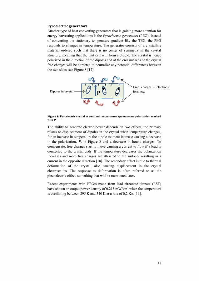
Pyroelectric generators Another type of heat converting generators that is gaining more attention for energy harvesting applications is the Pyroelectric generators (PEG). Instead of converting the stationary temperature gradient like the TEG, the PEG responds to changes in temperature. The generator consists of a crystalline material ordered such that there is no center of symmetry in the crystal structure, meaning that the unit cell will form a dipole. The crystal is hence polarized in the direction of the dipoles and at the end surfaces of the crystal free charges will be attracted to neutralize any potential differences between the two sides, see Figure 8 [17].
Figure 8: Pyroelectric crystal at constant temperature, spontaneous polarization marked with P
The ability to generate electric power depends on two effects, the primary relates to displacement of dipoles in the crystal when temperature changes, for an increase in temperature the dipole moment increase causing a decrease in the polarization, P, in Figure 8 and a decrease in bound charges. To compensate, free charges start to move causing a current to flow if a load is connected to the crystal ends. If the temperature decreases the polarization increases and more free charges are attracted to the surfaces resulting in a current in the opposite direction [18]. The secondary effect is due to thermal deformation of the crystal, also causing displacement in the crystal electrostatics. The response to deformation is often referred to as the piezoelectric effect, something that will be mentioned later.
Recent experiments with PEG:s made from lead zirconate titanate (PZT) have shown an output power density of 0.215 mW/cm3 when the temperature is oscillating between 295 K and 340 K at a rate of 0,2 K/s [19].
P Dipoles in crystal Free charges - electrons, ions, etc.

18
Radio Frequency With today’s usage and future development of wireless connectivity, such as mobile phones, WIFI-distributors and television, the air is filled with electromagnetic energy. For example the frequency bands around 2.1 GHz is occupied with 3G radio signals which are radially spread from mobile phones all around. By collecting this energy it is possible to create self-sustaining technology that can be used in wireless networks such as nodes in an alarm system [20]. For a schematic overview refer to Figure 9.
Rectenna By collecting the radio frequencies with an antenna, the energy can be converted into DC power using a rectifier. The amount of power given to the storage element and the load, Pdc is dependent on the available RF power in the environment, PRF and the conversion efficiency of the rectifier, ηRF/DC see Equation 9 [21].
In free space the energy from a transmitted signal decreases with the distance according to Equation 10 where Pr is the available power at the output terminal of the receiving antenna, Pt is the power fed into the transmitting antenna at its input terminal. Ar and At is the effective area of the receiving respectively the transmitting antenna, λ is the wavelength and d is the distance between the antennas [22].
Equation 10 is only valid for free space transmissions. In reality multi-path fading such as reflections from water and terrestrial objects like buildings and mountains, will have a significant negative effect on the received power.
Figure 9: Highly occupied frequency bands in Sweden a) outdoor b) indoor [86]

19
The available power at the output terminal depends mainly on the incoming power to the antenna, but also on the shape and size of the antenna as well as the impedance matching between the antenna and the rectifier. A typical antenna and rectifier circuit can be seen in Figure 10. The antenna to rectifier part of the circuit is often referred to as a rectenna [23].
Figure 10: Model of a rectenna
Since the location of the ambient RF-transmitter is unknown it is advisable to use an omnidirectional antenna to gather power in all directions, even though this choice of antenna decreases the gain. The antenna also has to be able to handle very low input power since the ambient radio electromagnetic energy is low. As already mentioned, the next step in the receiver chain that has an impact on the output power from the rectenna is the impedance matching between the antenna and the rectifier. An optimized impedance matching ensures the maximum power transfer, although it introduces some energy-losses [21].
State of the art in RF-collection Examples of available RF energy in the environment for specific frequency bands can be seen in Table 3 [24]. The values are measured at the Imperial Collage in central London and the values indicate that the power extracted with radio electromagnetic energy harvesting is not high enough for practical use today.
Table 3: RF energy in the air at the Imperial Collage in London [24]
Frequency bands Effect (nW/cm2) GSM900 48 GSM1800 50 3G 3

20
But with optimization of rectennas Piñuela et. Al. [24] shows in their recent work that RF-energy harvesting is capable of competing with known energy harvesting sources like thermal elements and PV-cells in the future. Piñuela et. Al. [24] also shows the possibility to extract energy from different frequency bands simultaneously by connecting rectennas via separate power manager connected to the same wireless microsystem. Another thing to study more in the future is the power/area- ratio. It has been shown that an increase of 83% in the area of the antenna results in a 300 % increase in power [25].

21
Other sources
Mechanical solutions Nearly all conventional methods to generate electricity involve a step where kinetic energy is converted into electric energy. Oil-, coal-, gas- and nuclear power plants all heat water to produce steam which in turn drives a generator. The same goes for wind and hydro power plants that utilize kinetic energy of flowing fluids to generate electric power. On a smaller scale there is a lot of kinetic energy being generated in everyday life that goes to waste as heat or sound, that includes vibrations from machines, opening of doors, humans in motion and cars braking to name a few.
As with the power plants, some kind of conversion is needed to be performed in order to turn this kind of kinetic energy into electrical energy. One problem when converting between these energy forms is how to do it without affecting the source in a noticeable manner. If clothes designed to harvest energy from human limb motions are heavy or stiff, it would be very tiresome to wear them.
The following chapter is intended to give a brief presentation of methods and techniques to turn motion into electricity.
Piezoelectricity Piezoelectric materials have the ability to generate electric current when subjected to mechanical force. The mechanism behind piezoelectricity is similar to pyroelectricity, and in fact all pyroelectric materials are also piezoelectric (the opposite is not true, there are piezoelectric materials that are not pyroelectric). Like in pyroelectric materials, the crystal unit cells form dipoles and when subjected to mechanic force the dipoles will line up and a voltage is built up along the dipoles in the crystal.
In energy harvesting applications several suggestions for implementations of piezoelectric materials have been proposed, for instance: scavenging heel impact of humans in motion [26] [27], vibrational monitoring [28] and flapping “leafs” that harvest wind energy by stretching and deforming thin films of piezoelectric material [29].
Recent advances in nanotechnology have enabled the manufacturing of piezoelectric structures that can be made flexible and a research group in Korea has developed a piezoelectric generator based on PZT nanowires deployed on a plastic substrate. The generator is paper thin and measures 3.5 cm x 3.5 cm, still they claim to output around 200 Volt of open circuit peak voltage from one bending cycle, resulting in a power density of 17.5 mW/cm2 [30].

22
Doors The energy needed to open or close an ordinary door at home is in most cases negligible but the movement reassembles a rotation, which easily can be converted to electrical energy by use of a standard generator. In a situation where the user can accept to put more effort in maneuvering the door such generators can be installed.
Experiment found in literature indicates that with a non-optimized generator, driven by the door movement, managed to extract 0.79 J of energy from one single opening [31]. On the other hand the effort to open the door went from 0.4 N applied force without the generator installed to 8.8 N with the generator attached. According to the study users started fell strain when more than 2 N of force was needed to open a door.
Water flow in domestic pipes The water flow in ordinary household pipes holds a potential source of energy that can be harvested by letting the water drive a generator. To not impair with the main function, to supply water, the generator must be designed such that it do not reduce the water flow substantially leading to a trade of between power generation and available water flow after the generator.
One example of such generator intended for domestic use, shows a maximum power generation of 720 mW at a flow rate of 20 l/min. Without generator the static pressure in the water pipe was 4 bar and with the generator installed the pressure dropped 2.2 bar at a flow rate of 20 l/min [32]. By careful design such generator could be useful for powering a wireless senor node that monitors water consumption.
Magnetic energy surrounding appliance cords Some home appliances demands almost constant power supply in order to function, mainly the fridge and the freezer. Surrounding a power supply conductor carrying an AC-current a magnetic field will be present and by inserting an inductor into this magnetic field a voltage can be generated over the inductor.
The voltage generated is proportional to the rate of change of magnetic flux acting on the inductor and it can be expressed as shown in Equation 11.
If an inductor with N turns, and cross sectional area A is placed perpendicular to the magnetic field the resulting magnetic flux will be equal to Equation 12.

23
For an infinite conductor the magnetic flux density B in a point at the distance r from the conductor can be expressed as in Equation 13.
Where μ0μr is the magnetic permeability, I0 is the peak current going through the conductor, ω the frequency of which the current alternates.
The induced voltage can then be stated as Equation 14.
From the Equation 14 it is seen that the larger the inductor, placed as close as possible to the conductor, the higher the induced voltage will be.
One of the main problems when trying to implement this technique is that almost all power cords have one active conductor and one return conductor running in parallel, meaning that at one given point on the cord there will exist two magnetic fields with opposite directions, canceling each other out. Despite this, experiments have still been conducted in order to examine the possibilities of this energy harvesting methods [33].
If the two parallel conductors are separated far apart, it has been shown that a 4.5H inductor placed 2.5 cm from a cord carrying 8.4 A of current can generate a power equal to 0.4 mW [33].
Another research group has constructed a wireless sensor node intended to monitor the current level in a conductor, which get all its power from the magnetic field surrounding the cord [34].
Summary of Energy Harvesters From a WSN point of view and in the scope of this project some harvesters may be excluded for use in this project due to very low output powers or practical issues. RF harvesting is promising, but the technique is still on a research level. The amount of energy that can be extracted is also very location dependent and hard to define. The harvesters mentioned in Other sources are all very conceptual and would require effort in developing the harvester rather than implementing energy harvesting in a WSN. The only harvester from this chapter that could be of interest is the piezoelectric harvester, which is commercially available. But the requirement of constant mechanical action to generate energy, make them hard to fit into a WSN designated for households. The two remaining harvesters to work with in this project are the PV-cell and the TEG, where the PV-cells seams more suitable due to higher efficiency compared to a TEG. But since the PV-cells lose their energy source during the night, the ability to buffer energy is crucial. With a strategic positioning the TEG could potentially produce energy continuously reducing the circuit complexity and cost for such

24
implementation. Table 4 summarize the three main sources considered in this project
Table 4: Summary of considered harvesters in this project.
Harvester Potential
power available
Reported efficiencies Pros Cons
Solar 100 mW/cm2 Up to ~40% Unlimited
during daylight
Intermittent supply
TEG Dependent on temperature difference
10-15% of Carnot
efficiency with ZT = 1
Possibility of
supplying constant power if placed
strategically
Require high
temperature gradients to be efficient.
RF
Dependent on location and frequencies
in use, Typically
around 50 nW/cm2
Up to 70 % [35]
Possibility of
supplying constant power if placed
strategically
Power decrease rapidly
with distance
from transmitter

25
Power management In a WSN, the sensor node typically alternates between different states, such as: read and process sensor data, transmit the data to central node or listen for incoming data. To keep the overall power consumption down the module can also go into various sleep modes where unnecessary units are switched off. Depending on the application, the time spent in the various states will vary and the power demand will change accordingly.
In an energy harvesting system the power source will have a varying ability to supply electricity depending on the environmental conditions. At some point the generated voltage may be too low for the system to run at all and at other times the input voltage may be higher than demanded, which may lead to surplus energy being wasted.
Just connecting the wireless sensor node directly to the harvester is hence an ineffective solution. Instead some kind of buffering solution between the generator and the consumer that can make the most out of the energy harvested would be more appropriate. Useful techniques to accomplish this will be presented in this chapter.
DC-DC converters
Step up Boost converter: principle of operation Today a typical microcontroller and radio module requires at least an input voltage of around 2 volts. This means that if the voltage generated from a harvester is below this required voltage it needs to be stepped up in order to be useful. One way of doing this is by using a boost converter, which in its simplest form could look like the circuit in Figure 11 [36].
The Pulse Width Modulation (PWM) unit generates a square wave which turns on and off the MOSFET Q with a duty time D, given in Equation 15.
The MOSFET Q in Figure 11 will act as a switch responding to the output from the PWM unit and alternate the circuit between two states. One state, in which the switch is closed, thus drawing current through the inductor down to ground, charging the inductor, a second state where the switch is open,
Q1
Vout Vin
PWM
VL
Figure 11: A simple DC-DC Boost converter

26
discharging the inductor through the diode towards the load. The purpose of the diode is to prevent current from flowing back to ground when the switch turns on again. When the switch is closed the capacitor on the output will make sure that the output voltage is held. The two states are illustrated in Figure 12 and Figure 13 respectively.
If the current IL is constantly kept above zero the boost converter is said to operate in continious mode and the circuit analysis will be as follows.
When the switch conducts the voltage over the inductor will be as in Equation 16.
The change in current IL can then be expressed like in Equation 17.
The current will increase linearly and peak just before the switch opens and the energy stored in the inductor will be as expressed in Equation 18.
Rl
L
IL
Vout Vin L
VL
IL
Rl
L IL
Vout Vin L VL
IVL
Figure 12: Simplified circuit of the boost converter with the switch closed
Figure 13: Simplified circuit of the boost converter with the switch opened

27
As the switch opens the current will be forced to make its way through the diode (which for now is assumed to have no voltage drop) and down to ground via the capacitor and the load. The change in current IL can then be derived from the expression for the voltage drop VL over the inductor formulated in Equation 19.
The resulting changes during one cycle must be zero, yielding the following expression stated in Equation 20.
As can be seen in the equation above, for a boost converter operating in continuous mode, the output voltage will go towards infinity as the off-time approaches zero which is the same as having the duty cycle approach 1.
If the current through the inductor is allowed to drop to zero during the time when the switch is open, the boost converter operates in discontinuous mode. To analyze this circuit, the off-time must be divided in two periods, one where the current drops from the peak value down to zero, toff1 and one period that starts as the current has reached zero and ends as the switch changes state, toff2. See sketch in Figure 14.
Red: switch timing Black: inductor current
toff1 toton
k: indu
f1 toff2
time
Figure 14: Timing diagram when operating in discontinuous mode

28
The overall expression for the output voltage will be slightly different in this mode. The current through the inductor will rise from and fall to zero hence the current increase will also be the peak current. Using the same equation as in the continuous case we know that the output voltage will be equal to Equation 21.
The only difference is that the fall time is now slightly shorter and is hence denoted toff1.
For a complete switching period Ts (Ts = ton + toff1 + toff2) the average current being consumed at the output can also be expressed as Equation 22.
Where Ipk is the peak current generated in the inductor and the expression is essentially the integral of the current during the period toff1 divided by the whole switching period. Using Ohms law and the previous expression for the peak current, the expression can be rewritten as Equation 23.
Where Rl is the load resistance and the two expressions containing Vout can both be solved for toff1 and then be set to be equal to each other, resulting in Equation 24.
Where f is the switching frequency being the inverse of the switching period Ts. Solving this for Vout result in Equation 25.
The output voltage in discontinuous mode will be a function of not only the duty time and input voltage but also the load resistance, the switching frequency and the inductance at the input.
Choosing what mode to operate in is more of a design issue and depends on the application. Discontinuous mode tend to require a larger inductor in order to provide the same current at the output compared to a converter operating in continuous mode. On the other hand in continuous mode the transfer function will contain a right half plane zero which can cause instability and also limits bandwidth [37]. Small loads also tend to make it

29
hard to operate in continuous mode and since the current will decrease very rapidly this can cause a very high voltage to be generated over the inductor.
Step down Buck-converter: principle of operation It may seem a bit on the contrary to mention step down converters in the scope of energy harvesting, since mostly the voltages generated are small, but during the occasional times when more energy is being harvested than what is being consumed, instead of just dissipating it as heat in the circuits, storing it for later use would be a much more efficient strategy. One way to do this is to have the boost converter, described previously, to charge a capacitor with as high voltage as possible. The motivation for doing this is the fact that the energy stored in a capacitor, expressed in Equation 26, is proportional to the voltage squared.
Since the voltage stored in the capacitor then can reach levels well above the microprocessors maximum input voltage, hence a way of reducing the voltage without significant losses is now needed. A common method of doing this is to use a so called Buck-converter; the circuit of a simple one can be found in Figure 15 [38] and compared to the boost-converter it uses similar components, but they are laid out differently.
Like the boost converter, the buck converter can also be operated in continuous and discontinuous mode and the approach to derive the expression for the final output voltage follows the same procedure as for the boost converter, the detailed steps are therefore omitted. For continuous operation the output voltage is expressed in Equation 27.
And in discontinuous mode, Equation 28 states the output voltage.
As can be seen from the expression the output voltage is again a function of the inductor size L, the load resistance Rl and the switching frequency f [38].
RL
Vout VL
Vin
PWM
L
Figure 15: Buck converter circuit diagram

30
Efficiency of DC-DC converters It is important to keep in mind that the described circuit cannot generate power itself, so in an ideal converter the available power at the output is the same as the power going in. If the voltage is higher at the output the current must decrease in order for energy equilibrium to be maintained. In a practical realization of a boost converter the components will be associated with certain losses that will affect the overall efficiency. The efficiency, η can be expressed as the ratio between the output power and the input power, see Equation 29.
In both converters there are losses caused by the diode forward voltage drop and internal resistance, the inductors equivalent serial resistance, transistor on-resistance, and parasitic capacitance from various sources in the circuit mainly from the diode and the transistor. Also the PWM-module needs to be powered in order to generate its output signal. The converters are also most likely used in an application where both input and output voltages are known, at least within what range. In order to regulate the output the PWM-unit takes a feedback sample as input and adjusts the duty time and/or switching frequency.
Due to the principle of operation of the converters, where they charge and discharge the inductor relative to the switching frequency, the voltage drop over the inductor will not be constant and the output voltage will vary accordingly. To counter this effect a capacitor is put in parallel to the output and the size of the capacitor is usually a design issue, depending on the frequency and desired output voltage.
Various methods exist to increase the efficiency of DC-DC converter; one way is to not only vary the pulse width of the PWM-unit but to also change the frequency of the pulse train. This is called to operate in Pulse Frequency Modulation mode (PFM). For both the buck and the boost converter this technique shows improved efficiency over a wider range and a well optimized converter can reach levels above 90% when implementing this method [39] [40].
Maximum Power Point Tracking Another important consideration is to make sure that as much power from a harvester is being transferred to the input of the power management circuit as possible. The maximum power transfer theorem states that maximum power is being transferred when the load resistance is exactly equal to the source resistance. This theorem can effectively be used when the source is a thermoelectric generator (TEG) since it can be modelled as an ideal voltage source in series with an internal resistance [41]. Refer to Figure 16.

31
Figure 16: Equivalent circuit of TEG
The power being transferred to the load, for instance the input of a power management circuit, is equal to Equation 30.
The derivative with respect to load resistance Rl when keeping the voltage constant will result in Equation 31.
The extreme value for Equation 31 is found when Rl is equal to Rs and when this condition is fulfilled the maximum amount of power is transferred from the source to the load and the system is said to be operating at the Maximum Power Point (MPP).
From simple voltage division the voltage present at the load then, is equal to half the TEG’s open circuit voltage. In the case with the TEG the open circuit voltage depends on difference in temperature and so does the internal resistance Rs. To keep maximum amount of power present at the load when the source resistance varies the resistance at the load must be able to vary accordingly.
Many algorithms to track the power point exists for instance the Open Circuit (OC) method [42]. This algorithm starts by disconnecting the load from the source and measure the open circuit voltage being generated at the source, hence the algorithm name. The sampled open circuit voltage is stored in a high performance capacitor and the load is connected again as quickly as possible. If the source is known to be a TEG the algorithm should be set to adjust the input resistance in such way that the resulting input voltage is equal to half the sampled open circuit voltage. When done the algorithm waits for a preset time period before it repeats. The drawback of this algorithm is mainly that it disconnects the load from the source allowing no power at all to be delivered to the input and it does so at repeated time period regardless if the voltage has changed or not.
Rl
RS I
VTEG
Vl

32
This algorithm also needs to take into account what source that is currently supplying the power. The TEG equivalent model is simple whereas the PV-cell requires a more complex model and the maximum power point depend on more factors. An equivalent circuit of a PV-cell that yields sufficient accuracy, is a current source in parallel with a diode and a resistance all together in series with a resistance, compare with Figure 17 [43].
Figure 17: Equivalent circuit for a PV-cell
Using Kirchhoff’s Current Law (KCL) it can be seen that the resulting current I, going into the load is equal to Equation 32
Where Ipv is the current being generated from incoming light, Id is the current through the diode and Ish is the current through the shunt resistance. The diode current in the circuit can be expressed as in Equation 33.
The current I0 is the reverse bias current and is dependent on physical properties of the pn-junction, Vd is the applied voltage and will in this case be the sum of the voltage over the load and the voltage over the serial resistance, n is the diodes ideality factor, k is the Boltzmann constant and T is the temperature in Kelvin. The shunt current is simply the same voltage as over the diode divided by the shunt resistance, using Ohm’s law.
The current being supplied to the load can then be rewritten like Equation 34.
As can be seen the ability to supply current is nonlinearly dependent on the output voltage V. A generic sketch of how the current with respect to output voltage looks can be seen in Figure 18. The figure assumes a constant light radiation and constant temperature.
V
I
Rs
Rl Rsh D
Ish Id
Ipv
Id h

33
Figure 18: Illustrative plot of an IV-curve for a PV-cell
Figure 19: Power delivered to load attached to a PV-cell
Figure 19 depicts the resulting power being consumed at the load under the same conditions as in Figure 18 and as can be seen it reaches a maximum power, marked MPP in the figure, below the open circuit voltage.
Compared to the TEG the photovoltaic cell exhibits a more complicated IV-curve demanding more from the power point tracking algorithm. Though experiments has shown that the maximum power point will be positioned around 73-80% of the open circuit voltage [44], hence the OC-algorithm may still be used for PV-cells if the load resistance is set to be around 80% of the sampled open circuit voltage. The OC-algorithm is easy to implement but due to the fixed division ratio it may not always hit the exact MPP. Using more advanced algorithms efficiencies of up to 97% can be achieved [45].
Current Curre
Voltage
Voltage
Power Pow
V
MPP

34
Storage elements From time to time there will most certain be situations when there is no energy to harvest. For solar powered applications this problem will arise every night and depending on geographical location the length of one night will vary with season. To overcome this problem, there is a need for an energy buffer that can supply power when there is no energy to scavenge from the environment. An ideal storage element is one that could store a high amount of energy without being bulky, can be charged with low currents, show no leakage discharge when not in use and last for an infinite number of charge-discharge cycles without losing capacity.
Today there are mainly two different elements to choose from, namely the rechargeable battery and the supercapacitors. The following chapter will describe their function, advantages and disadvantages.
Rechargeable Batteries Rechargeable batteries store its energy in an electrochemical nature using a construction called an electrochemical cell, consisting of an anode, a cathode and an electrolyte. Several topologies for making a rechargeable battery exist, and the most common includes: Lead-Acid, Nickel Cadmium, Nickel Metal Hydride, Lithium Ion, Lithium Polymer and Lithium Iron Phosphate [46].
The voltage generated from a cell is determined by the ability of the anode to emit electrons through an oxidation reaction and the cathodes ability to attract electrons via a reduction reaction. When defining these abilities, they are always stated as reduction reactions with reference to a hydrogen electrode and is called standard electrode potential or standard reduction potential (E0) and it is given in Volts. For a given cell the theoretical voltage generated is stated in Equation 35.
Some standard electrode potentials for common battery technologies are listed in Table 5 [47].

35
Table 5: Standard reduction potentials for common battery technologies
Battery technology Reactions (formulated as reductions) E0 (V)
Li -3.05
Ni-Cd +0.48
Ni-Cd -0.82
Lead-Acid +1.70
Lead-Acid -0.35
When measuring the actual voltage from such cell it will deviate slightly from the theoretical value. This deviation can be calculated using Nernst’s equation which takes the concentrations of the electrochemical components into account, and since these change during discharge the voltage will vary over time. An indication of how the voltage varies with respect to the remaining capacity for various technologies is found in Figure 20.
Figure 20: Cell Voltage as a function of capacity discharged for various cell chemistries [48]

36
It can be seen in this diagram that rechargeable batteries generates a nonlinear output voltage during discharge, with an initial drop when first connected, followed by an almost constant output voltage, and when the capacity is about to run out the voltage rapidly decreases again. The ability to supply an almost constant voltage, not directly proportional to the capacity is a highly desirable property of batteries.
Lithium based batteries As can be seen in Table 5, lithium has a high standard reduction potential making it a very suitable component of a battery, as can be seen in Figure 20, the output voltage is almost twice as high compared to other topologies. From the periodic table it is also known to be the lightest of all metals, resulting in high energy content per unit weight.
The working principle for lithium ion batteries is the flow of positive lithium ions through an electrolyte when an external circuit is connected to the anode and cathode electrodes. The positive electrode is often made of lithium cobalt oxide (LiCoO2) [49] and the negative is made from graphite. When charging the battery, that is applying an external voltage to the battery cell, lithium ions will start to migrate from the positive electrode via the electrolyte (often made from lithium hexafluorophosphate ( LiPF6) dissolved in ethylene carbonate) and intercalate3 in between the graphite sheets, increasing the potential energy of the lithium ions. When a load is connected to the cell, electrons will start to flow in that external circuit from the negative electrode to the positive due to the potential difference and electric field, this will cause lithium ions to return to the positive electrode via the electrolyte in order to even out any free charges caused by electrons [50].
The number of charge-discharge cycles a lithium ion cell can undergo is limited and one of the main limitations is the degradation of the graphite anode. When the cell is charged for the first time the electrolyte will form a film around the graphite that functions as a permeable layer for lithium ions but is non permeable for electrons [51]. This layer is fundamental for the function of the cell but will grow thicker over time and increase the internal resistance of the cell. The intercalation of lithium ions will also cause deformation of the graphite lattice and eventually cracks may form resulting in lower ability to hold ions resulting in a loss of overall capacity.
Due to the high reactivity of lithium there is risk of rapid increase in temperature if not handled appropriately. Several manufacturers recalled products containing lithium ion batteries when the technology was new in mid-1990 due to thermal runway and cells catching fire [52]. Despite advances in safety mechanisms to prevent excessive heat, and a deeper insight in the cells inner workings, accidents with lithium ion still occurs.
3 Intercalate: when particles is reversibly inserted into a layered compound.

37
To safely and effectively charge lithium ion batteries additional circuitry is needed. The theoretical charge profile diagram for lithium ion batteries, Figure 21, states how to safely charge the cell without degrading the performance.
The first period called trickle charge is only applicable when the cell has been deeply discharged, below 3 V [53]. If the cell voltage start to reach 2.5 V, irreversible damage may occur [54] hence protection circuitry is needed to shut off the load in time. The charge current is normally given as a percentage of the cells maximum capacity denoted C, for a 1000 mAh cell 1C corresponds to a charge (or discharge) current of 1000 mA. A trickle charge current of 0.1C is advisory for lithium ion cells [53].
Current
Voltage
End of charg
Trickle charge
Constant current Constant voltage
Figure 21: Theoretical charge profile for Lithium ion batteries [53] [55]
Time

38
In most cases the charging start with a constant current around 1C [55] where the cell voltage is rising to its maximum value (4.2 V) [53] and when reached the charger should go into a constant voltage phase while decreasing the charge current. The constant voltage needs to be very accurate (within 1 %) since overcharging risks to cause damage to the cell and undercharging will reduce the maximum capacity at a more rapid rate than normal ageing [53].
From the datasheet of two commercially available lithium ion cells, it can be found that after 300-500 charge-discharge cycles the maximum capacity has dropped almost 30 % [56] [57].
The need for a special charging circuit when dealing with lithium ion batteries increases the overall complexity and cost of the final application. There will also be a reduction in the charging efficiency since some of the supplied power will be dissipated in the additional charge components.
Supercapacitors Traditional capacitors store energy in an electrostatic way by the buildup of an electric field between two conductive plates separated by an insulating layer. The capacity of such device can be expressed as in Equation 36.
The capacity is given in Farads, F and is a measure of stored charge Q with respect to applied voltage V. The amount of energy, E, that can be stored in such capacitor can be derived by integrating the amount of charges stored for a given voltage, using the expression 36 the energy will be as follows in Equation 37.
These expressions are also valid for supercapacitors, a subclass of capacitors with significantly higher capacity than traditional capacitors. Their principle of operation can be divided into three categories, electrochemical double layer capacitance, pseudocapacitance and a hybrid of them both [58]. Commercially available supercapacitors can have an energy density of around 5 Wh/kg [59] compared to lithium ion batteries that can have more than 200 Wh/kg [60].
Electrochemical double layer capacitors uses porous carbon based electrodes (often made from burnt coconut shell [61]) placed in an electrolyte separated by a membrane. When a voltage is applied to the carbon electrodes, charges in the electrolyte will be attracted to them, no recombination occurs as for batteries, instead a double layer is formed. The main reason for the increase in capacity is due to the porosity of the electrodes giving them a very large surface (reports claim 1640 m2/g [62]) and hence a large amount of charges can be held. Also since no materials are physically affected the reverse

39
reaction is easy to perform and the number of charge-discharge cycles could reach well above 100 000.
Pseudocapacitance arises when ions in the electrolyte reacts with surface atoms on the electrode. For pseudocapacitors the electrodes are made from conducting polymers or metal oxides [58]. The mechanical stress seen on conductive polymers during charge and discharge limits their lifetime and for metal oxide electrodes the most potential material is ruthenium oxide, a limited and thus very expensive material.
In hybrid solutions, capacities well above the double layered types can be achieved while still maintaining mechanical stability.
The main disadvantages for supercapacitors are their limited maximum voltages and linear discharge profile. Supercapacitors using organic electrolytes the maximum applicable voltage before breakdown is 2.7 Volts. To counter this, four capacitors can be used, two pairs of series connected capacitors, connected in parallel, resulting in a maximum capacity of 5.4 Volts and with the capacity maintained, trading of space and cost.
Summary of Energy Storage Lithium ion batteries main advantage is the ability to supply a constant voltage, not directly dependent on capacity left as opposed to supercapacitors, which shows a linear discharge profile. But charging lithium ion batteries requires more care to be taken in terms of controlling the charge voltage and current. This is something that could be difficult to maintain in an energy harvesting application, where a constant supply of power not can be guaranteed. Charging and discharging will also reduce the maximum capacity at a higher rate for lithium ion batteries compared to supercapacitors. Based on this, supercapacitors were chosen as the energy storage element in this project.

40
Microcontrollers In electronic circuits used to send and receive data in any way, the need for a controlling unit and data storage is of essence. Since Intel released their first microprocessor, the 4004 in 1971, the microprocessor industry has grown fast. When Intel released their first microcontroller in 1974, the 8080, which had all functions of a computer on one chip, and new era of low cost electronics began [63]. In a wireless microsystem such as a node in an alarm system the requirement of a low-power consuming microcontroller with sufficient performance is desirable.
The power consumed by a microcontroller is the product of the operating voltage and the consumed current. To be able to decide which microcontroller to use in a wireless microsystem, the power consumption is a key parameter, and a suitable strategy to compare microcontrollers is to make a power budget. Since wireless microsystems are used in situations where the system is put in a low power mode most of the time, it is important to make a good approximation of the time spent in different modes and then make a power. In a typical application the wireless microsystem is in its active mode 10 % of the time which gives a power budget as in Figure 22.
To lower the power consumption both the consumed current and the operating voltage should be considered. The consumed current is closely related to the system clock frequency and the current external peripherals may consume. Higher system clock frequency and peripherals, such as oscillators and memories, increases the overall current consumption. In addition to this, the current consumption can increase due to leakage current in the circuit, which often is a product of temperature, supply voltage or process technologies. Operation voltage can also be lowered for power reduction [64].
In excess of the power consumption, there are other factors to consider when choosing a microcontroller to be used in a wireless microsystem; microprocessor capability, memory sizes, peripherals and their interfaces, number of input/output-pins as well as the interrupts handling [65].
Figure 22: A typical power budget for a wireless microsystem
Active mode (10% of the time)
Average current Low-power mode

41
The central processing unit (CPU) is the heart of the microcontroller. It is common to compare the clock frequencies of CPUs, with the highest frequency giving the fastest processor. But one should be aware that some CPUs can execute more than one instruction per cycle making them faster or slower than their frequency shows. The CPU also has another important aspect when it comes to power-consumption. In the active mode, the CPU can complete the designated task fast, in expense of more power consumption than if it runs slower. But in the fast mode the microprocessor can go to a less power-consuming mode faster, which may lower the overall power consumption of the microcontroller. The CPU can also have a Reduced Instruction Set Architecture (RISC) which means that the cycles per instruction are reduced in consequence of increased number of instructions per program. Often this leads to an overall decreased operating time for the CPU, which in turn decreases the overall power-consumption [66]. The operating time for a CPU is given in Equation 38.
When the microcontroller is used in specific applications, the sizes of memories such as ROM (read-only), RAM (random-access) and flash-memories are of importance. If a large amount of data and instructions are going to be used, the memories should be bigger than if the application only requires small amount of stored data and instructions.
The next step is to decide the required peripherals such as the capability and number of oscillators, timers, analog-to-digital converter and also which interfaces their data transfer is compatible with. One common way of interfacing external devices to the microcontroller is via the protocol Serial Peripheral Interface (SPI), which is explained in Appendix 1.
The number of I/O-pins is also crucial for communication and integration of the microcontroller into a microsystem. Furthermore the interrupt handling is of importance since the microcontrollers often are used in low power-devices, where it takes too much power to constantly check what is happening on pins or bits. Instead, a part of the microcontroller works as a specialist, with the main function to react when something happens and at that time send a signal to the microprocessor which can react correctly on the specific interrupt. Last but not least the price and physical size of the microcontroller are also of significance [67].
There are great amount of microcontrollers suitable for usage in a wireless microsystem. In Appendix 2 a selection of low power-consuming microcontrollers, available on the market today, is described. Table 6 summarizes the relevant properties serving as material for the choice of the microcontroller to be used in this project.

42
Table 6: Performances and prices of four microcontrollers [68]
Run-mode (mW)
Low-power mode (μW)
GPIO-pins
Flash (kB)
RAM(kB)
Price (sek/500
-999 pieces)
MSP430G2xxx 9.56 0.22 8-24 1-16 0.256
-0.512
17.32
LPC81xM 4.62 0.561 6-18 4-16 1-4 7.38
AT32UC3Axxx 29.7 46 69-109 0.128
-0.512
32 or 64 71.15
STM32L100x 14.04 0.90 37-51 32-128
4-10 13.06

43
Wireless connectivity The main energy consumer in a Wireless Senor Node is the transceiver part; some exceptions do exist such as cameras and other units performing heavy signal processing. A short summary of the basics in wireless digital communication can be found in Appendix 2 where concepts as Modulation, Bit Error Rate and Energy and Bandwidth efficiency are explained.
In Table 7 a comparison between commercially available radio modules for low power applications operating at the ISM-bands around 900 MHz (center frequency at 868 MHz in Europe and at 915 MHz in USA) is found, and it can be seen that they all support binary FSK, also called 2-FSK. One method to decrease frequency spreading when the transmitter changes between the symbols is to output the frequency in a Gaussian pulse instead of a square pulse, this modulation is then denoted 2-GFSK
Table 7: Comparison of commercially available radio modules
Supp. Volt. (V)
Tx. curr. 868 MHz (mA)
Rx. curr. (mA)
Sleep curr. (μA)
Max. Out. power (dBm)
Max. data rate (kbps)
Modulation supported
TI CC1201
[69]
2,0 - 3,6
46 (14
dBm) 23,6 0,3 16 1250
2-(G)FSK, 4-(G)FSK,
MSK, OOK
HOPE RF RFM69C
W [70]
1,8 – 3,6
45 (13
dBm) 16 0,1 13 300
(G)FSK, (G)MSK,
OOK
HOPE RF RFM12B
[71]
2,2 – 3,8
23 (7
dBm) 12 0,3 7 115,2 2-FSK
Analog devices
ADF7021-NBCPZ
[72]
2,3 - 3,6
32,3 (10
dBm) 22,7 0,1 13 24
2FSK, 3FSK, 4FSK, MSK
ST SPIRIT1 QTR [73]
1,8 – 3,6
44 (16
dBm) 9,7 0,85 16 500
2-(G)FSK, (G)MSK,
OOK, ASK
To decrease the overall power consumption of the WSN one can increase the time between transmissions and listening events. During transmission the main power consumer is the power amplifier delivering the signal to the antenna and also decides the range of the communication link.

44
Design Phase
Software The software developed for the project made use of the Serial Peripheral Interface- protocol, to communicate with the radio module, for details regarding SPI see appendix 1. With the LPCXpresso LPC810 code base, available free of charge from NXP:s homepage, we developed a code written in the language C, suitable for low power management of a microcontroller as well as firmware for a transceiver radio module. The goal was to produce a transceiver capable of two-way communication, with focus on fast change between different modes for the radio module.
Two code examples were developed with special features for the two radio modules. For the TI CC1201 this meant implementation of the enhanced Wake up Radio-mode (eWOR), where the radio module alternates between receive mode and sleep mode without interactions from the microcontroller. For the RFM69CW a corresponding mode, called ListenON, where used. The two modes are further on referred to as the listen-modes. While the radio modules are in their listen-modes the microcontroller is put in a low power-consuming mode where the Windowed Watchdog Timer (WWDT) and the Brown Out Detector (BOD) are disabled. From this mode the wake-up is triggered by the Wake Up Timer (WKT).
Due to the listen-modes the microcontroller can stay in power-down mode until it gets an interrupt from the radio module to wake it up when there is a message in the FIFO-register to be read or until the WKT has timed out. This leads to a decrease in the overall power consumption in the system. When a message has been read the system transmit a message telling, for example the gateway, that it has received data. To create a more realistic two-way communication the system applies a LAT-segment.
After power up the microcontroller initializes the radio module and a message is transmitted. Then the system enters the eternal loop which starts with a power-down of the microcontroller while the radio module enters the listen-mode. If the radio does not receive a message while in listen-mode the microcontroller is woken up by the WKT after three minutes and a message is transmitted. Thereafter a LAT-segment is run before the microcontroller puts the radio module in listen-mode again and then goes back to power-down mode.
If however the microcontroller is woken up by the radio module due to a received message in the listen-mode the system will read the received message and then transmit an answer (resend). After this the microcontroller uses the LAT-segment before it restarts the eternal loop. The stages of the developed code can be seen in Figure 23.

45
Figure 23: Stages of the microcontroller and the radio module.
A power-budget for the system can be seen in Figure 24.
Figure 24: Power budget for the radio module and microcontroller.
Before the stages in Figure 23 were developed we made use of deeper power-down methods, but due to instability they were excluded in the final system.

46
Data A typical packet to be sent or received in a WSN contains a preamble word, sync word, address to a specific node, the actual data and last a cyclic redundancy Check (CRC). The preamble is used to make it easier for the receiver to know when to start listening for a sync word, which in turns are the bytes of data telling the receiver that the message is intended for the specific node. An address word can also be used to target a specific receiver in a big net of nodes that are listening for a packet. The length of the data to be transmitted can either be incorporated in the data as the first byte/bytes if the system is using variable packet length. If, on the contrary, the system is using a fixed packet length both the transmitter and the receiver know how many bytes the data contains and there is no need for a length byte. Last is the CRC-byte which is an algorithm to detect bit-errors in the packet.
A process that can be used to improve the packet quality is whitening. In the whitening process the data and CRC are exclusive-or’d (XOR) with a pseudo-random sequence before transmission. When the packet is received by the receiver the data is XOR’d with the same pseudo-random sequence which results in the original data. This operation makes the data bits that are transmitted random and DC-free which improves the transmission since the power is distributed over the occupied bandwidth as well as it prevents the possibility of data decencies in the receiver control loop [74].
In this project all parts of a packet described above is included except the address bytes. The packet is configured to contain 3 bytes of preamble, 4 bytes syncword, 10 bytes of data and 2 bytes of CRC, which can be seen in Figure 25.
Figure 25: The packet structure used for transmitting and receiving data in this project
Texas Instruments CC1201 RF Transceiver After discussions with Verisure Innovation AB we decided to incorporate the transceiver CC1201 from Texas Instruments in our design to make it more compatible with the product line of the company. CC1201 is a well-documented transceiver operating at sub gigahertz frequencies. The correct configurations in respect of frequencies, deviation, output power and other important settings for transmitting and receiving data can be collected from the windows application SmartRF Studio from Texas Instruments. SmartRF Studio lets the user configure the radio module in use and the register settings can then be exported and implemented for use in source code of the device. The settings used in this project are stated in table 8.

47
Table 8: Settings for radio module CC1201
The mode that the CC1201 is currently in, is easily changed with the single byte command strobes and in this project four modes is used: transmit-, receive-, listen- and idle mode. In transmit-mode the current-consumption should be typically 46mA at 3 V of supply-voltage, 25 ºC and an output power of +14dBm. In receive-mode the current-consumption is nearly the same as in transmit-mode with the same conditions. The Idle-mode current consumption is typically 1.5 mA. In listen mode the current-consumption is the sum of the consumptions in the idle-, sleep- and receive-state with the percentage of each in respect to the time spent in each mode.
A photo of the test-setup using the CC1201 radio can be found in Figure 26.
Figure 26: One of our prototypes equipped with a Texas Instruments CC1201 radio-module
Frequency (MHz)
Deviation (kHz)
RX BW- Filter (kHz)
Modulation format
Rb
(kbps) Output power (dBm)
868.0 20.0 104.2 2-GFSK 38.4 7

48
HopeRF RFM69CW RF Transceiver The modes used for the transceiver RFM69CW are the same as for CC1201: transmit-, receive-, listen- and idle mode. According to the datasheet the current consumption is 45 mA in transmit-mode with the output power set to 13 dBm, 16 mA in receive-mode and 1.2 μA in idle-mode. The current consumption in listen mode is equal to the sum of the consumptions in the idle- and receive state. The settings we used in the final implementation can be seen in Table 9.
Table 9: Settings for radio module RFM69CW
Unfortunately we could not get the listen mode for the RFM69CW to work properly since the transceiver got stuck in the receive-stage. To be able to do realistic and comparable measurements anyway we programmed the microcontroller to put the RFM69CW in receive-mode for 200 milliseconds once every 30 seconds and transmits a message each third minute. A typical test set-up for our PCB with the RFM69CW and a solar cell as the power source can be seen in Figure 27.
Figure 27: Test set-up with the radio module RFM69CW and microcontroller LPC812
In the beginning of the project we used a predecessor to the RFM69CW, namely the RFM12B, also from HopeRF. The plan was to use the RFM12B for the final prototype, but it went out of stock during the project. Due to this we only used the RFM12B in transmit mode to make some initial tests.
Frequency (MHz)
Deviation (kHz)
RX BW Filter (kHz)
Modulation format
Rb (kbps)
Output power (dBm)
867.9 20.0 100 2-FSK 38.4 7

49
Hardware
Power management circuitry After reading other reports about energy harvesting in WSN, we soon realized that we would need some sort of power management circuitry. Texas Instruments provided us with free samples of the BQ25570 integrated circuit evaluation board. The BQ25570 is marketed as an “Ultra Low Power Harvester Power Management IC with Boost Charger, and Nanopower Buck Converter”. The IC features an Open Circuit MPPT algorithm sampling every 16 seconds, supports input voltages down to 100 mV while still outputting up to 5.5 V, to charge for instance a supercapacitor or a lithium ion battery. From the storage element the IC has the ability to provide a regulated output voltage via a buck converter. The current consumed by circuit itself is rated to be 488 nA.
The BQ25570 also features a pin where one can select either 50% or 80% MPPT, by pulling the pin low respectively high. After some successful testing with an evaluation board we decided to use BQ25570 as the power management circuit in our project programmed to output a constant voltage of 2 V.
Energy Storage We were convinced from the very beginning that we wanted to utilize supercapacitors as our storage solution. If carried out correctly with respect to charging, a lithium ion battery would probably be more reliable during times of low or no input power, but its limited life time related to the limited number of charge-discharge cycles would potentially result in costly service issues of the nodes at shorter intervals compared to supercapacitors.
We picked three different supercapacitors with a maximum voltage of at least 5 Volts and they can be found in Table 10 [75] [76] [77].
Table 10: Supercapacitor used in this project
Manufacturer Capacity (F)
Max. Volt. (V)
Internal Resistance
(Ω) @ 1kHz
Capacity Tolerance
(%)
Price (SEK)
Cooper Bussmann
1.5 5.0 0.31 -10 to +30 66.78
Kemet 2.2 5.5 35 -20 to +80 84.20
Cooper Bussmann
5.0 5.4 0.065 -10 to +30 92.22

50
Schematic From our tests with evaluation boards we constructed a schematic for our final prototype, the whole schematic can be found in Appendix 1. The software we used to generate it is called “CadSoft EAGLE PCB Design”, a program we had previous experience from and felt comfortable to work with.
As can be seen in the schematic it consists of two major parts, the left side contains the power management circuitry and the right side the microprocessor and radio modules. The power management circuitry was to a large extent laid out with inspiration from the reference design, featured in the datasheet of BQ25570 with some adjustments for our needs and available stock from the electronic component supplier. Additionally, we added the possibility to update the flash memory of the microprocessor through a six pin header. But since the USB to serial cable uses an output voltage of 5 V which is too high for our chosen microcontroller, a low drop out voltage regulator was installed to bring down the voltage to 3.3 V when updating the firmware.
Built into the BQ25570 is a feature to monitor if the storage element is above a certain voltage level, programmable by the user. The pin that governs this feature is called VBAT_OK and can be found on the right side of the BQ25570. Our intention was to feed this to our microprocessor to safely turn it off when voltage dropped to critical levels and wake up the processor when there was enough energy in the storage element to power the system up again without risking ending up in an oscillating state where the system load would just drain the storage element when charging with small amounts of power. The designated wake-up pin on the microcontroller required an inverse of the output from VBAT_OK to function as we desired, hence we inserted an inverter in form of a pulled up N-MOSFET where VBAT_OK was feed to the gate and the inverse signal was taken from the drain of the N-MOSFET. Unfortunately we did not manage to realize this function in a way where we saw a significant performance gain. Since this part of the circuitry has no function in the final prototype the signal path has been cut off.
We had two radio modules to benchmark and since we wanted to reuse as many signal paths as possible to save space on the final PCB the signals to the CC1201 are fed through the pads of the RFM69CW via zero ohm jumpers, clearly outlined in Figure 28. The zero ohm jumpers allow us to cut off the signals to the CC1201 connector if we want to build a board with the RFM69CW module. When the board was mounted we run into problems regarding the enable signal and it turned out that we had routed it to an input-only pin on the microprocessor. To solve this we inserted a patch cable to reroute this signal path to another pin. The solution is visible in some of the photos of the final prototype.
For verification purpose we installed test points for the input voltage (Vin), capacitor voltage (Vbat) and the regulated output voltage (Vout).

51
Printed circuit board From the schematic we used the same software to generate a layout for a final printed circuit board. To fit everything in we used both the top- and the bottom layer for routing but only the top layer was used for the placement of components. It is a common strategy to use one layer for horizontal signal traces and one layer for vertical, something we tried to follows as far as possible. The final layout can be found in Figure 28 and 29.
Figure 28: Top layer of our circuit board
Figure 29: Bottom layer of our circuit board
This design was then submitted to the PCB manufacturer Cogra Pro AB and after a week we received six copies of our design.
The components was hand soldered with hot air, a new experience for us, and the first assembled prototype might have suffered some damage during the soldering since it broke down after some use for no apparent reason. Especially the BQ25570 which came in a five by five millimeter Quadrature Flat No-Lead package (QFN) required some practice before we got it in place.
CC1201 RFM69CW

52
Apart from the breakout headers, input- and storage connectors all components was chosen to be surface mounted and the complete bill of materials (BOM) for the prototype can be found in Appendix 2.
A schematic of our final prototype, with the chosen components can be seen in Figure 30.
Figure 30: Our final prototype
Load
BQ25570
PV-cell Boost
converter Buck
converter LPC812
Supercapacitor
CC1201 / RFM69CW c
BQ 0
Buck 2
SPI

53
Measurements and Results To get an insight of available energy during a day a test was run overnight with a large PV-cell rated at 800 mW supplying power to a BQ25570. This in turn distributed the energy to charge the supercapacitor of 1.5 F, and supplied the node, using the RFM12B radio module, with power. The result from this measurement is seen in Figure 31.
Figure 31: An overnight test between February 26 and February 27 using PV-cell as harvester, BQ25570, Cooper Bussmann 1.5F supercapacitor, LPC810 and RFM12B in transmit only mode.
The initial test reveals that such large PV-cell is more than sufficient for supplying power; hence we decided to focus on smaller PV-cell in further tests. We used two small and cheap PV-cells with the characteristics as found in Table 11. The ripple seen in the Vin voltage in Figure 31 originates from the MPPT-algorithm.
Table 11: The two PV-cells used in the experiment
Name Size
(cm x cm) VOC (V)
ISC
(mA)
Velleman Sol1 4.6 x 7.2 0.5 400
Velleman Sol4 6.6 x 9.5 2 200
To find out what power they were able to supply we connected the PV-cells to various resistors of increasing values and the voltage was measured over this load. They were tested under two different light conditions. The light intensities was measured to 500 lux indoors and 25 000 lux in direct sunlight behind a window. The resulting Power versus Voltage curves from this test can be found in Figure 32.

54
Figure 32: Performance characterization of two of our PV-cells that were used in this project (Note that the difference between the y-axis scales is on the order of a factor 100 between indoor and direct sunlight conditions).
From this test the maximum output power per square centimeter, for indoor lightning were found to be:
In sunlight the maximum power per square centimeter were found to be:
To find the input power, where our two different prototypes are fully functional and the capacitor voltage neither charge nor discharge, we used a Power Supply Unit (PSU). We adjusted the input power until we reached equilibrium between the input power and the power being consumed. For our prototype using the Texas Instruments radio, it turned out to be 2.3 mW and with the RFM69CW radio the equilibrium power was 1.0 mW.
Due to the significant difference in equilibrium power we wanted to compare the range when transmitting in order to make sure that the TI module is not far superior when it comes to propagation. We set up the modules next to each other and placed a receiver approximately 100 meter away in an office environment. This simple test revealed that the received messages had about equal signal strengths and hence the results from each module can be compared to each other, but keep in mind that they use different antennas something that may affect both range and power consumption.

55
We wanted to benchmark our two prototypes under same conditions hence we chose an input power where both would have a surplus of power to charge the capacitor and the input power was set to 3.5 mW. See Table 11 for all test circuit values.
Table 11: Settings for the charging measurements
Open-circuit
Voltage
MPPT VIN (V)
Input Current
(mA)
Input power (mW)
R1 (ohm)
R2 (ohm)
0.7 50 % 0.35 10 3.5 39 0.1
There were two scenarios of interest to be measured on our proof-of-concept node; the charge time and time to failure without input power for the three super capacitors mentioned in the previous chapter. The measurements where made with the super capacitors connected as the energy storage to our prototypes and the radio modules working as described in the Software part of the design phase chapter. In the charge part of the measurements we used a PSU to be able to make comparable tests with a continuous constant input power.
A simple schematic of our measurement arrangement can be seen in Figure 33. To simulate a typical energy harvester we used a PSU with resistance connected in series with the input. We set the PSU to an open circuit voltage of 0.7 Volts which is a reasonable value compared to our chosen PV-cells. By varying the series resistance, R1 we were able to regulate the current going in, and by that also the power. To measure the current we installed a low ohmic precision resistor, R2 in series with the PSU. Since the power source now is mainly resistive we set the MPPT-algorithm on our prototype to 50 %. The symbols marked VIN, VBAT, VOUT, and GND represents the test points mentioned in the PCB-chapter that we connected our measuring equipment to.
Figure 33: Test setup for charging the super capacitor
Since we were to deal with quite lengthy tests we needed measuring equipment that could supervise the voltage levels of interest over a long

56
period of time. We did not find any reasonably priced solution to this so we decided to develop our own. Using the microcontroller prototyping board from Arduino we wrote a firmware that samples the voltages of interest using the microprocessor’s 10 bit Analog to Digital converter (ADC) and sends the sampled values serially over USB to a host application that writes these to a text file along with the current time. This text file could then be analyzed in MATLAB. The host application was develop using the programming language C# and features a Graphical User Interface (GUI) where we could live monitor our test. A screenshot from this application in action can be seen in Figure 34.
Figure 34: Screenshot from our log-application
Since a final product must be designed from the intended harvester and with the available power over time in consideration we found no point in making tests with other input power levels instead the charging and discharging behaviors are intended to be used more as guidelines when designing a final devices. These tests were performed with our two different prototypes configured and running as described in the software part
For the test with 3.5 mW of input power we defined the rise time as the time it takes to charge a supercapacitor from 2 volts to 4 volts, starting on 2 volts because only above that level will we have our desired output voltage and stopping at 4 mainly to save some time due to the exponential charging behavior of a capacitor. Following charts, Figure 35 and 36 show the charging behavior with the three different supercapacitors connected to the prototype with the radio module from TI respectively Hope RF.

57
Figure 35: Charging the prototype with the TI CC1201 radio attached, with three different supercapacitors at 3.5 mW of input power.
Figure 36: Charging the prototype with the Hope RF RFM69CW radio attached, with three different supercapacitors at 3.5 mW of input power.
To determine the time to failure when all inputs is disconnected the time to discharge the supercapacitor from 5 to 2 volts was measured. Figure 37 and 38 shows the discharging behavior of the two prototypes and the time to failure, for each capacitor.

58
Figure 37: Test to find the time to failure when input power is lost for the three different supercapacitors with the TI CC1201 radio module attached.
Figure 38: Test to find the time to failure when input power is lost for the three different supercapacitors with the Hope RF RFM69CW radio module attached.
We also wanted to run our prototypes using TEG:s as the energy harvester hence we did some measurements with a small TEG (1.5 cm x 1.5 cm) its hot side attached to a radiator and its cold side fitted with aluminum cooler fins. We used an Infrared- camera (IR-camera) and measured the radiator surface to be 32 ̊C and the cooler fins to 24 ̊C. This temperature gradient of 8 ̊C yielded an open circuit voltage of 0.09 Volt and a short circuit current of 64 μA which would result in too low power to be useful for our prototypes.

59
Discussion Throughout the whole project we have worked from a very broad perspective regarding the concept Energy Harvesting, in an attempt to make the best possible proof of concept. We wanted to try at least three types of harvesters: a rectenna for RF-, a TEG for thermal- and a PV-cell for solar - harvesting, preferably in combination with each other to have a constant energy supply. After studies in the literature we realized that RF-harvesting is not a practical option at the present time. The basic experiment we did with the TEG indicated that we would need many of them to get a reasonable amount of energy. Due to their high cost per unit, together with the need for additional mechanics to carry the heat away and support the elements we ruled them out for further testing. The only source left was the PV-cell and hence we shifted our proof of concept design towards operating with them as the energy source.
Our test with the RFM12B seen in Figure 31, shows how the available solar power will vary during a typical February day and with this in mind, we chose the components to account for fluctuations of energy over time. This turned out to be our only design limit and in retrospect it would have been more useful to have set up further specification regarding the intended node. If one decides to use PV-cell as harvesters a power budget would be suitable to establish in advance to both make sure that the energy stored will last and that the charging is complete before sunset. Further specifications could be a defined radio protocol including what information and at what intervals the nodes shall communicate.
From Figure 32 it is found that the incoming light in indoor conditions for a reasonably sized PV-cell is not yet sufficient for powering our prototypes, however close to a window there is more than enough during daylight. Looking further at the graphs in Figure 32 it can be found that all of them have a peak power at around 73 - 80 % of the open circuit voltage as mentioned in the theory, supporting the use of the MPPT-algorithm set to 80%. When comparing the shapes of the power-voltage curves between indoor and sunlight conditions, it is seen that when the incoming intensity is high the generated power increases more linear up to the maximum power point. This corresponds well with the theory behind Equation 34 in the MPPT-chapter. From the equation it can be seen that if the Ipv is large, the ability to supply current will be stronger and can withstand the opposing diode and shunt resistor currents longer.
When designing a node to be powered by a PV-cell it is important to account for the lack of input power during nights. From the Figures 37 and 38 we can see how the time to failure for the two radio modules depends on the attached supercapacitor. From these various times one can get an indication of how large the supercapacitor needs to be in terms of capacity. This states how much energy that is needed to be input during the charging period, for example during daylight for solar harvesters. The results from the charging experiments, see Figure 35 and 36, gives a good indication if it will be

60
possible to reach this amount of energy when charging with a fairly low power.
When comparing the discharge Figures 37 and 38, it can be seen that even if the initial voltages differs slightly in favor for the TI CC1201 radio, the Hope RF RFM69CW outperforms TI with approximately three times longer time to failure. This performance factor holds for the charging times as well except for the smallest supercapacitor. Reasons for this variation could be from the various starting voltages which impacts smaller capacitors more due to a higher charging rate related to the RC-constant of capacitors. Also there is a plateau in the RFM69CW charging curve for unknown reasons resulting in a longer charging time.
When charging and discharging the prototype using the 2.2 F supercapacitor, one finds sudden drops in the capacitor voltage. Our theory to this behavior is based on the higher internal resistance of said capacitor compared to the other two as seen in Table 10. When the supercapacitor is connected to the prototype there will be a smaller capacitor of 100 μF connected in parallel. The smaller capacitor will probably discharge quicker than the supercapacitor during system loads, which shifts the voltage in the storage node until the supercapacitor can level out the difference. With higher internal resistance in a capacitor the charge/discharge time will increase hence it seems like a plausible explanation for the voltage drops.
Challenges One obstacle was the lack of documentation for the Hope RF radios leading to a lot of trial and error programming making us spend quite some time when trying to interface them. None of us had experience of writing C code directly to a microcontroller and the provided user manual was overwhelming and took some time to get used to. Another obstacle was the implementation of the third radio module, the TI CC1201, which our supervisor strongly suggested us to use quite late into the project something that increased the workload and the need for even more software to be developed.
When testing our final prototype, we ran into a problem where the output voltage from the BQ25570 dropped as soon as the supercapacitor reached the target voltage, while still having input power present to the BQ25570. Due to this we could not do any tests over a long period of time with our prototype connected to a solar cell. We think one reason for this behavior could be that when we did tests with the evaluation board we did not consider one part of the circuit named V_STOR, which is the input node to the buck-converter. According to the datasheet of BQ25570 there should be capacitors placed close to the V_STOR pin. Unfortunately we missed this part and the capacitors ended up far from the pin in our layout. Another datasheet miss was the SPI-enable signal path that ended up on an input only pin on the microcontroller. Lesson learned: “Read datasheets twice!”

61
Suggestion for further research From a software point-of-view there are a few developments that could be done to make the proof-of-concept node and the tests more realistic. For starters, the proof-of-concept node should be developed with a specific application in mind, and the timings and packet length should correspond exactly to the ones used in a specific area of the WSN. Additional low power-modes, such as the deep-power down-mode for the microcontroller LPC812 described in the design-phase, should be investigated and integrated to extend the life-time of the node when the input-power is low or zero. The input power could also be monitored and be used as an indicator for the microcontroller to enter different stages of low power-consuming modes or regulate the time spent in high power-consuming modes. Another software implementation could be an energy harvester specific control, for example a node driven by a solar cell could use a mode selector linked to the amount of hours of sunshine regulating the system load based upon this.
To further expand WSN to include sensors with need for heavy signal processing, the possibility to send the sensors raw data to be processed by the central node should be evaluated. For this it may be necessary to investigate other modulation schemes to reduce transmit time while maintaining a low power consumption without losing performance.
When designing our proof of concept we worked from the requirements of using a microprocessor with a core from ARM to ease the integration with Verisures Innovation AB product line. By broadening the perspectives and evaluating other architectures a more suitable processor might be found. Same goes with the radio solution and power management; we were very biased towards Texas Instruments and due to their well-established business relation with Verisure we got a lot of free samples to work with, limiting us from further comparisons with competitors on the market.
One of the motivations to the project was to reduce the amount of battery replacements in an installed node and if one successfully does so it would be of interest to find out how much actually could be saved in terms of real money.
Summary of discussion Overall we are satisfied with the outcome of this project; we have effectively shown that it is possible to power a wireless sensor node with an input power that is possible for an energy harvester to achieve. But there is still a lot of further testing to do in order to make a final product, especially one must specify the application and perform long running test with the intended harvester as power supply. From the test we did it seems like that Hope RF RFM69CW is the go to solution but one should keep in mind the lack documentation and support which is far better for the TI CC1201.

62
References
[1] F. Lewis, "Wireless Sensor Networks," The University of Texas at Arlington, Texas, 2004.
[2] B. M. D. G. Jennifer Yick, "Wireless sensor network survey," Computer Networks, no. 52, pp. 2292-2330, 2008.
[3] S. B. Christiana Honsberg, "PV EDUCATION," [Online]. Available: http://pveducation.org/pvcdrom/solar-cell-operation/efficiency. [Accessed 08 05 2014].
[4] O. C. O. Alireza Khaligh, Energy Harvesting : Solar, Wind, and Ocean Energy Conversion Systems, CRC Press Inc, 2009.
[5] G. P. Smestad, Optoelectronics of solar cells, Bellingham, Wash.: SPIE, 2002.
[6] N. Sridhar, "Understanding Photovoltaics and the Market Forces Behind Them," Texas Instruments, 2011.
[7] V. P. J. S. Rupesh Manak, "Nanomodules - Solar Energy Harvesting Devices," International Journal of Current Engineering and Technology, vol. 3, no. 5, pp. 1672-1678, 2013.
[8] K. E. Y. H. W. W. E. D. D. Martin A. Green, "Solar cell efficiency tables," Progress in Photovolatics: Research and Applications, no. 22, pp. 1-9, 2014.
[9] R. N. O. S. D. S. E. R. H. Lund, "Solar Cells," Norwegian University of Science and Technology, 2008. [Online]. Available: http://org.ntnu.no/solarcells/pages/generations.php. [Accessed 08 05 2014].
[10] G. C. M. D. Zhifeng Ren, THERMOELECTRICS AND ITS ENERGY HARVESTING: MODULES, SYSTEMS,AND APPLICATIONS IN THERMOELECTRICS, Boca Raton, FL: CRC Press, 2012.
[11] H. J. Goldsmid, Introduction to Thermoelectricity, Springer, 2009.
[12] M. Li, "Thermoelectric-Generator-Based DC-DC Conversion Network for Automotive Applications," KTH Information and Communication Technology, Stockholm, 2011.
[13] Micropelt GmbH, Datasheet: TGP-751 / TGP-651, Freiburg, Germany, 2013.

63
[14] Thermalforce, Datasheet: Thermo Electrical Generator TEG 017-150-29, Berlin, Germany.
[15] S. E. C. T. O. B. Venkatasubramanian Rama, "Thin-film thermoelectric devices with high room-temperature figures of merit," Nature, vol. 413, no. 6856, pp. 597-602, 2001.
[16] J.-S. L. M. M. Keivan Davami, "Nanowires in Thermoelectric Devices," Transactions on Electrical and Electronic Materials, vol. 12, no. 6, pp. 227-233, 2011.
[17] S. B. Lang, "Pyroelectricity: From Ancient Curiosity to Modern Imaging Tool," Physics Today, vol. 58, no. 8, pp. 31-36, 2005.
[18] J. H. J. ,. B. K. Y. ,. F. Z. ,. K. C. P. ,. W. G. ,. Z. L. W. Ya Yang, "Flexible Pyroelectric Nanogenerators using a Composite Structure of Lead-Free KNbO3 Nanowires," Advanced Materials, vol. 24, no. 39, pp. 5357-5362, 2012.
[19] S. W. Y. Z. Z. L. W. Ya Yang, "Pyroelectric Nanogenerators for Driving Wireless Sensors," Nano Letters, vol. 12, no. 12, pp. 6408-6413, 2012.
[20] M. H. Cohen.Patent US7400253 B2, 2008.
[21] F. D. M. L. L. D. BOUCHOUICHA, "Ambient RF Energy Harvesting," International Conference on Renewable Energies and Power Quality, Granada, 2010.
[22] H. T. FRIIS, "A Note. on a Simple Transmission Formula," Proceedings of the I.R.E. and Waves and Electrons, vol. May, 1946.
[23] K. M. T. F. Triet Le, "Efficient Far-Field Radio Frequency Energy Harvesting for Passively Powered Sensor Networks," IEEE JOURNAL OF SOLID-STATE CIRCUITS, vol. 43, no. 5, pp. 1287-1302, 2008.
[24] P. D. M. S. L. Manuel Piñuela, "Ambient RF Energy Harvesting in Urban and Semi-Urban Environments," IEEE TRANSACTIONS ON MICROWAVE THEORY AND TECHNIQUES, vol. 61, no. 7, 2013.
[25] A. Harb, "Energy harvesting: State-of-the-art," Renewable Energy, vol. 36, pp. 2641-2654, 2011.
[26] D. Fourie, "Shoe-Mounted PVDF Piezoelectric Transducer for Energy Harvesting," Massachusetts Institute of Technology, Massachusetts, 2012.

64
[27] D. B. L Moro, "Harvested power and sensitivity analysis of vibrating shoe-mounted piezoelectric cantilevers," Smart Materials and Structures, vol. 19, no. 11, 2010.
[28] N. K. D. S. H. D. J. I. Dao Zhoua, "A Self-powered Wireless Sensor Node for Structural Health Monitoring," Health Monitoring of Structural and Biological Systems, vol. 7650, 2010.
[29] H. L. Shuguang Li, "VERTICAL-STALK FLAPPING-LEAF GENERATOR FOR WIND ENERGY HARVESTING," in Proceedings of the ASME 2009 Conference on Smart Materials, Adaptive Structures and Intelligent Systems , Oxnard, California, USA, 2009.
[30] J. H. S. ,. G.-T. H. ,. C. K. J. ,. J. R. ,. M. K. ,. I. C. ,. S. H. L. ,. M. B. ,. Z. L. W. ,. a. K. J. L. Kwi-Il Park, "Highly-Effi cient, Flexible Piezoelectric PZT Thin Film Nanogenerator on Plastic Substrates," Advanced Materials, vol. 26, no. 16, pp. 2514-2520, 2014.
[31] X. Zhu, "Human Power Door Opening Harvester," Department of Electrical and Computer Engineering, Urbana, IL, 2008.
[32] A. W. R. G. P. B. B. F. Y. M. D Hoffmann, "Energy Harvesting from Fluid Flow in Water Pipelines for Smart Metering Applications," in The 13th International Conference on Micro and Nanotechnology for Power Generation and Energy Conversion Applications (PowerMEMS 2013), London, UK, 2013.
[33] A. K. R. R. Vikram Gupta, "Energy Harvesting from Electromagnetic Energy Radiating from AC Power Lines," Carnegie Mellon University, Pittsburgh, PA, 2011.
[34] Y. W. P. L. S. P. Z. Z. D. Lu, "Self-contained Self-powered Wireless Sensing Node for AC Power Supply Cords Monitoring," in Progress In Electromagnetics Research Symposium Proceedings, Stockholm, Sweden, 2013.
[35] H. Ostaffe, RF Energy Harvesting: From Theory to Deployment, Powercast Corporation, 2011.
[36] Texas Instruments, Application Report: SLVA061, 1999.
[37] H. Yao, "Modeling and Design of a Current Mode Control Boost Converter," Colorado State University, Fort Collins, Colorado, 2012.
[38] Texas Instruments, Application Report: Understanding Buck Power Stages in Switchmode Power Supplies, SLVA057, Texas Instruments, 1999.

65
[39] X. W. Bi Zhuo, "A PWM/PFM switch technique of dual-mode buck converter," in Wireless Mobile and Computing (CCWMC 2009), Shanghai, 2009.
[40] P.-H. C. J.-C. T. Wan-Rone Liou, "A synchronous boost regulator with PWM/PFM mode operation," in ASIC, 2009. ASICON '09, Changsha, Hunan, 2009.
[41] V. C. N. W. M. H. B. O. C. O. Wensi Wang, "Thermoelectric Energy Harvesting for Building Energy Management Wireless Sensor Networks," International Journal of Distributed Sensor Networks, vol. 2013, 2013.
[42] R. F. S. L. A. DOLARA, "Energy Comparison of Seven MPPT Techniques for PV Systems," JEMAA, vol. 1, no. 3, pp. 152-162, 2009.
[43] Z. K. D. N. Dominique Bonkoungou, "Modelling and Simulation of photovoltaic module considering single-diode equivalent circuit model in MATLAB," International Journal of Emerging Technology and Advanced Engineering, vol. 3, no. 3, pp. 493-502, 2013.
[44] M. H. M. S. J. Ali Reza Reisi, "Classification and comparison of maximum power point tracking techniques for photovoltaic system: A review," Renewable and Sustainable Energy Reviews, vol. 19, no. March 2013, pp. 433-443, 2013.
[45] R. M. Hohm D.P, "Comparative study of maximum power point tracking algorithms using an experimental, programmable, maximum power point tracking test bed," in Photovoltaic Specialists Conference, 2000. Conference Record of the Twenty-Eighth IEEE, Anchorage, AK, 2000.
[46] N. Kularatna, "Rechargeable Batteries and Their Management," IEEE Instrumentation & Measurement Magazine, pp. 20-33, 2011.
[47] S. A. H. R. V. K. Katerina E. Aifantis, High Energy Density Lithium Batteries: Materials, Engineering, Applications, Wiley-VCH Verlag GmbH, 2010.
[48] B. Lawson, "Electropedia," [Online]. Available: http://www.mpoweruk.com/performance.htm. [Accessed 09 05 2014].
[49] B. Scrosati, "Recent advances in lithium ion battery materials," Electrochimica Acta, vol. 2000, no. 45, pp. 2461-2466, 2000.
[50] Panasonic, Overview of Lithium Ion Batteries, Panasonic, 2007.
[51] I. R. Mattson, "Stability of the Graphite Electrode for Li-ion Batteries," NTNU - Trondheim, Trondheim, 2013.

66
[52] R. R. T. P. K. P.G. Balakrishnan, "Safety mechanisms in lithium-ion batteries," Journal of Power Sources, vol. 2006, no. 155, pp. 401-414, 2006.
[53] B. D. C. T. W. R. S. Valle, "An ultra-compact and efficient Li-ion battery charger circuit for biomedical applications," in Proceedings of 2010 IEEE International Symposium on Circuits and Systems, Paris, France, 2010.
[54] F. Hoffart, "Proper Care Extends Li-Ion Battery Life," Power Electronics Technology, vol. 2008, no. April, pp. 24-28, 2008.
[55] H. Grewal, Li-Ion Battery Charger solution using the MSP430, Texas Instruments, 2005.
[56] Panasonic, Datasheet: Lithium Ion UR18650A, Sanyo Energy, 2012.
[57] Varta Microbattery GmbH, Datasheet: LIC 18650-22 FC, Ellwagen, Germany: Varta Microbattery GmbH, 2010.
[58] J. C. E. Marin S. Halper, "Supercapacitors: A Brief Overview," MITRE, McLean, Virginia, USA, 2006.
[59] Illinois Capacitor, inc, DCN Super Capacitors, Lincolnwood, Il: Illinois Capacitor, inc.
[60] Panasonic, Datasheet: NCR18659F, Panasonic, 2012.
[61] R. D. Lawrence Weinstein, "Supercapacitor carbons," Materials Today, vol. 16, no. 10, pp. 356-357, 2013.
[62] S. T. Amrita Jain, "Fabrication and characterization of energy storing supercapacitor devices using coconut shell based activated charcoal electrode," Materials Science and Engineering: B, vol. 183, no. April 2014, pp. 54-60, 2014.
[63] Intel, "Intel Timeline: A History of Innovation," Intel, [Online]. Available: http://www.intel.com/content/www/us/en/history/historic-timeline.html. [Accessed 08 05 2014].
[64] A. S. Arne Martin Holberg, "Innovative Techniques for Extremely Low Power Consumption with 8-bit Microcontrollers," Atmel Corporation, Tiller, Norway, 2006.
[65] Instructables, "Instrucables: How to choose a MicroController," [Online]. Available: http://www.instructables.com/id/How-to-choose-a-MicroController/. [Accessed 08 05 2014].

67
[66] P. Jain, "Engineers Garage ...inspiring creations," [Online]. Available: http://www.engineersgarage.com/articles/risc-and-cisc-architecture. [Accessed 08 05 2014].
[67] V. Soffel, "MicroController Pros Corporation," MicroController Pros Corporation, 01 05 2003. [Online]. Available: http://ucpros.com/work%20samples/Microcontroller%20Communication%20Interfaces%201.htm. [Accessed 08 05 2014].
[68] Farnell Element 14, "Farnell," [Online]. Available: http://se.farnell.com/?CMP=KNC-GSE-FSE-GEN-PFB&mckv=s6F3Mfprv|pcrid|20131908040|kword|farnell|match|e|plid|. [Accessed 20 03 2014].
[69] Texas Instruments, Datasheet: CC1201 Low-Power, High-Performance RF Transceiver, Texas Instruments, 2014.
[70] Hope RF, Datasheet: RFM69CW ISM TRANSCEIVER MODULE V 1.1, Shenzhen,China: Hope RF, 2013.
[71] Hope RF, Datasheet: RFM12B Universal ISM, Shenzhen,China : Hope Rf, 2011.
[72] Analog Devices, Datasheet: ADF7021-N, Norwood, MA, USA: Analog Devices, Inc, 2008.
[73] ST, Datasheet: SPIRIT1 Low data rate, low power sub-1GHZ transceiver, ST, 2013.
[74] G. Christiansen, "Data Whitening and Random TX Mode," Texas Instruments incorporated, Dallas, Texas, 2010.
[75] Cooper Bussmann, Datasheet: Supercapacitors PHV Series, Cooper Bussmann, 2011.
[76] Cooper Bussmann, Datasheet: Supercapacitors PHB Series, Cooper Bussmann, 2011.
[77] NEC/TOKIN, Datasheet: Supercapacitors, NEC/TOKIN, 2013.
[78] Diolan, "SPI Bus Interface," Diolan, [Online]. Available: http://www.diolan.com/dln_doc/spi-bus-interface.html. [Accessed 09 05 2014].
[79] Texas Instruments, "Mixed Signal Microcontroller," Texas Instruments Incorporated, 2013.
[80] NXP Semiconductors, "LPC81xM: Product data sheet," 2014.

68
[81] ATMEL, "AT32UC3A," Atmel Corporation, 2009.
[82] STMicroelectronics, "Ultralow power 32-bit MCU ARM®-based Cortex™-M3," ST Microelectronics, 2013.
[83] G. Lindell, Introduction to Digital Communications, Lund, Sweden: Lund University, 2006.
[84] J. R. T. Sasilatha, "Comparative Studies on the Performance of Low Power Transmitters for Wireless Sensor Nodes," Journal of Computer Science, vol. 5, no. 2, pp. 140-145, 2009.
[85] M. Padmavathy, "Performance Evaluation of Energy Efficient Modulation Scheme and Hop Distance Estimation for WSN," International Journal of Communication Networks and Information Security, vol. 2, no. 1, pp. 44-49, 2010.
[86] PTS Inriktningsplan för spektrumhantering, 2012.
[87] SMHI, "Strålning," SMHI, 05 2009. [Online]. Available: http://www.smhi.se/klimatdata/meteorologi/stralning. [Accessed 27 05 2014].

69
Appendices
Appendix 1
SPI Serial to Peripheral Interface, most known as SPI, is an easy to learn and well-known master-slave protocol for fast data transfer over short wired distances. Even though the SPI protocol is a widely used serial communication tool it does not have a formal standard, which gives the user an opportunity to configure it according to the components in use. The most important thing to take into consideration is the clock frequencies and the type of valid transitions of data for the components. There are four different modes of transitions where data can be latched. These are decided by combinations of CPOL and CPHA, refereeing to the SPI clock polarity respectively phases. With CPOL equal to one the data is latched at the clock falling edge, and with CPOL equal to zero the data is instead latched on the clock rising edge. This is true as long as CPHA is equal zero, but with CPHA equal to one the CPOL is reversed. See Figure 1 for a schematic description.
Figure 1: The function of the SPI clock polarity (CPOL) and phase (CPHA) [78]

70
In Figure 2 the four signal lines of the SPI protocol are outlined. MISO and MOSI stands for Master In Slave Out respectively Master Out Slave In. SCLK signifies the SPI Clock which drives the whole system, making synchronization easy. SSEL stand for Slave Select, which also can be named nSEL or Chip Select (CS). It is the slave select that indicates to the slave that the master wants to start communicating with this specific slave. This feature makes it is possible to have more than one slave connected to a master, all sharing the same signal paths for MOSI, MISO and SCLK [78].
Figure 2: The four communication lines of the SPI

71
Appendix 2
A collection of microcontrollers
MSP430G2xxx Texas Instruments popular MSP430G2xxx has been on the market for a long time, but it is still competing with new-comers with its low power consumption and architecture. The CPU in the microcontroller is a 16-bit RISC with 62.5 ns instruction cycle time, which corresponds to a 16 MHz clock frequency. The MSP430xx has five low-power modes with a power consumption of 0.22 μW in the deepest power-down mode, and 0.56 mW in active mode. The microcontroller supports UART, SPI and I2C and among the peripherals an A/D-converter, two 16-bit timers, an internal low-power oscillator and an internal digital oscillator can be found. The MSP430G2xxx can be purchased in a great amount of different packages with number of GPIO-pins ascending from 8-24 and a flash memory that spans from 1-16 kB with RAM in the sizes of 256-512 byte. There are some different interrupts that can be used to wake-up the microcontroller from low-power modes as well as indicate occurrences [79].
LPC81xM The LPC81xM is a microcontroller family presented by NXP. They contain the 32 bit RISC microprocessor ARM-Cortex™-M0+ running at frequencies up to 30 MHz The microcontroller has four low power modes with a typical power consumption of 0.561 μW at the deepest power-down mode and 4.62 mW in active mode. Some of the included peripherals in the LPC81xM are a Cyclic Redundancy Check (CRC) engine, a multi-rate- and a wake-up timer, a low-power oscillator as well as a comparator. The microcontroller also supports one I2C-bus, up to three USARTs and up to two SPI-interfaces. Flash memory from 4-16 kB is available for the different packages of the microcontroller, along with 1-4 kB of SRAM. The number of GPIO-pins varies from 6-18 and in the peripheral Switch matrix they are configurable in a very flexible way. In the microcontroller each peripheral has their own interrupt line which is connected to the Nested Vectored Interrupt Controller (NVIC). Each line can have several interrupt flags, giving the microcontroller a rich control over the processes. From low-power modes the LPC81xM may be woken by internal clocks or by an external interrupt on the wake-up GPIO-pin [80].

72
AT32UC3Axxxx This microcontroller from ATMEL is a low power AVR®32-Bit RISC microcontroller running at frequencies up to 66 MHz It has six less power-consuming modes where it can reach 46 μW in the lowest power-consuming mode is and in active mode the power consumption is around 29.7 mW. All these current- and power- consumption is measured with a system clock frequency of 12 MHz Some of the peripherals in the microcontroller are an A/D-converter, oscillators and timers, and the supported interfaces are SPI, USART and I2C among others. The internal flash memory spans from 128-512 bytes and the SRAM having sizes of 32 kB or 64 kB with the different packages, having 69-109 GPIO pins. The microprocessor can be woken by interrupts via the Interrupt Controller (INTC), which gets an interrupt signal from the peripherals or GPIO-pins and order them in levels before it alerts the microprocessor [81].
STM32L100xx The STM32L100xx-microcontroller is presented by STMicroelectronics. It has a RISC ARM-Cortex™-M3 microprocessor operating at frequencies from 32 kHz up to 32 MHz at maximum. The microcontroller has six low power modes with a power consumption of 0.9 μW in stand-by mode and 14.04 mW in active mode. Supported interfaces are three USART, two SPI and two I2C, and some of the peripherals in the microcontroller are a real-time clock (RTC), an A/D-converter and oscillators. The microcontroller has a flash memory of 32-128 kB, SRAM in the span of 4-10 kB and 37 or 51 GPIO-pins depending on the package. Analogous to the LPC81xM with an ARM-Cortex™-M0+, the STM32L100xx has a NVIC [82].

73
Appendix 3
Basics of digital wireless communication For a transceiver to send information to the network, it generates a pure analog carrier signal which it manipulates using a specific modulation scheme in accordance with the data being sent. A sinusoidal electromagnetically waveform has essentially three properties that can be affected in order for the signal to carry information that is the amplitude, frequency and phase. When digital information in form of binary bits is to be sent together with an analog carrier it is common to use modulation based upon the concept of keying, the word originates from the Morse code key used in telegraphs. Similarly to Morse code, where a sequence of sound pulses of two different lengths make up a symbol that can be deciphered using a key, digital modulation rely on skewing the analog carrier signal in discrete manner. The most basic modulation principles are called: Frequency Shift Keying (FSK), Phase Shift Keying (PSK), Amplitude Shift Keying (ASK) and Quadrature Amplitude Modulation (QAM). The methods modulates the carrier in the way the name indicate except QAM, which is more like a combination of PSK and ASK. It is then up to the receiver to decide what information that was sent by demodulating the received signal and recreate the sequence of bits that the transmitter sent.
Other types of modulation that most commercially available radio modules support is Minimum Shift Keying (MSK) with optional Gaussian pulse shape (GMSK) and On-Off Keying (OOK). MSK is basically a form of FSK, but where transitions between frequencies are done in the zero-crossing, eliminating discontinuousness in the carrier phase which otherwise will cause frequency spreading. OOK is a very simple modulation method similar to Morse code, where the bit value is represented with either presence of carrier wave or no presence of carrier wave. While being very simple to implement, OOK has a drawback in its susceptibility to noise
One problem in communications is to counter the effects of noise and disturbances along the communication path. When information is sent digitally there is a risk that the received signal is interpreted faulty, on a bit level this means that a sent 0 will be received as a 1 or the other way around. The bit error probability, Pb is a number describing the average number of incorrectly received bits per detected bit. The lower the Pb the less likely the receiver is to make a faulty decision. For instance if the transmitter outputs information with the bit rate, Rb = 100 kbps and the bit error rate is, Pb = 10-5 then for a constant bit stream during the time, t = 60 s the receiver will detect RbtPb = 105 ∙ 60 ∙ 10-5 = 60 bit errors. Depending on the application it may be an acceptable level of bit errors, but for really critical applications the bit error rate has to be decreased even further [83].
One parameter that has a strong influence on the bit error rate is the amount of energy that is used to describe the information, the more power that is used to output one bit or the longer the time one bit is sent the easier it will be for the receiver to separate the sent signal from noise and thus make a

74
proper decision. The bit error rate will then decrease if all other conditions remain the same. But increasing the power in one bit will also increase the total power consumption which is something that is particularly undesired in an energy harvesting system. If one modulation method can achieve a desired bit error rate while consuming less power than another method for same bit error rate, the first method is said to be more energy efficient.
Another important design consideration is to keep the occupied bandwidth, W at minimum, since there is a limited frequency spectrum available [83]. How effectively a signal constellation use the bandwidth can be expressed as in Equation 1 as the bandwidth efficiency, with the bitrate Rb.
Equation 1 indicates how many bits that can be sent per occupied Hertz of bandwidth, given in the unit bit/Hz. The more information a system can send per unit time while keeping the bandwidth as low as possible the more bandwidth efficient the system will be.
The simplest case of modulation is the binary case where one signal alternative, or symbol represents a “0” and another signal alternative represents a “1”. This principle can be extended further and instead of only two symbols each representing one bit, more alternatives can be used to represent a multiple of bits, if considering a 4:ary FSK constellation, one frequency would represent “00”, the second would be “01”, the third would be “10” and the fourth frequency would result in “11”. In this particular example, more information is sent per signal alternative. If the frequency separation is kept constant more bandwidth is occupied but if the separation is reduced to fit in a given bandwidth there will be a smaller margin between two consecutive signal alternatives, making such communication system more sensitive to noise. On the other hand, every sent symbol will consume the same amount of power in comparison with amplitude modulation where the transmitter has to increase the amplitude of the sent signal to represent various symbols and the average power consumption will increase when expanding the modulation scheme, assuming all symbols are equally likely to be sent. If instead PSK is used, the same energy per symbol is consumed, since only the phase is varied between the signal alternatives but the more symbols that are squeezed in, the closer they will be located to each other and more output power is needed to overcome noise disturbances. Comparing FSK and PSK there is also a difference in transceiver circuitry and PSK tend to use more components which in turn consumes more power [84].
For wireless sensor nodes that only transmit a small amount of data there is no need for high data rates. It is not until the transmit time, depending on the data length, reaches the time it takes for the radio module to wake up from sleep mode it will be of concern to use a higher order of modulation to decrease the overall transmit time [85]. With that said, it is most often

75
sufficient to use binary signaling which also keeps the circuit complexity down. If it is possible to trade off some bandwidth it is further beneficial to the power consumption to choose FSK.

76
Appendix 4
Figure 1: Schematic of or prototype

77
Appendix 5
Table 1: Bill of Materials
pric
e p.
u. (S
EK)
101,
53
13,7
7
- -
8,17
7,81
0,07
1
0,06
2
0,06
6
0,04
9
0,06
3
0,06
3
0,06
3
0,05
9
0,17
4
0,51
2,46
0,52
0,26
27,5
7
2,1
2,46
3,77
11,5
4,42
0,34
9,43
51,3
9
89,3
9
Art
icle
nbr
.
2373
545
2320
694
2287
688
2287
655
2140
980
2141
155
2141
123
2141
013
2141
130
2141
148
2141
129
2141
151
1469
661
1650
866
1886
132
9227
857
8819
980
9527
834
2112
852
1886
132
1845
739
1841
250
1608
281
1510
761
2100
300
1876
520
1801
742
Supp
lier
Farn
ell
Farn
ell
Idee
tron
TI
Farn
ell
Farn
ell
Farn
ell
Farn
ell
Farn
ell
Farn
ell
Farn
ell
Farn
ell
Farn
ell
Farn
ell
Farn
ell
Farn
ell
Farn
ell
Farn
ell
Farn
ell
Farn
ell
Farn
ell
Farn
ell
Farn
ell
Farn
ell
Farn
ell
Farn
ell
Farn
ell
Farn
ell
Farn
ell
Man
ufac
ture
r
TI NX
P
Hop
e R
F
TI
Coi
lcra
ft
Coi
lcra
ft
Vis
hay
Dra
loric
Vis
hay
Dra
loric
Vis
hay
Dra
loric
Vis
hay
Dra
loric
Vis
hay
Dra
loric
Vis
hay
Dra
loric
Vis
hay
Dra
loric
Vis
hay
Dra
loric
Vis
hay
Dra
loric
Kem
et
Joha
nson
Die
lect
rics
Kem
et
Mur
ata
Mur
ata
Taiy
o yu
den
Joha
nson
Die
lect
rics
Mur
ata
Wür
th
Om
ron
NX
P
Mic
rel
3M
Sam
tec
Size
QFN
-20
TSS
OP
-16
- -
3.9m
m x
3.9
mm
3.9m
m x
3.9
mm
402
402
402
402
402
402
402
402
402
805
603
805
603
1812
805
603
805
3.5
mm
pitc
h
6 m
m x
6 m
m
sot2
3
sot2
23
Valu
e
- - - -
22 u
H
10 u
H
330
Koh
m
8.2
Moh
m
4.7
Moh
m
590
Koh
m
5.23
Moh
m
7.15
Moh
m
5.11
Moh
m
7.68
Moh
m
0 oh
m
0.1
uF
0.1
uF
4.7
uF
0.01
uF
100
uF
4.7
uF
0.1
uF
22 u
F
- -
3.3
Vou
t
Des
crip
tion
Pow
er M
anag
er
mic
roco
ntro
ller
Rad
io
Radi
o
Indu
ctor
Indu
ctor
Res
isto
r
Res
isto
r
Res
isto
r
Res
isto
r
Res
isto
r
Res
isto
r
Res
isto
r
Res
isto
r
Jum
per
Cap
acito
r
Cap
acito
r
Cap
acito
r
Cap
acito
r
Cap
acito
r
Cap
acito
r
Cap
acito
r
Cap
acito
r
Term
inal
Blo
ck
Res
et S
witc
h
MO
SFE
T
Vol
t. re
gula
tor
Sili
cone
feet
,
Boa
rd to
boa
rd c
onn.
Circ
uit r
efer
ence
BQ
2557
0
LPC
812M
101J
DH
16
RFM
69C
W
TI C
C12
01
L1 L2
R1,
R9,
R10
, R11
, R12
, R15
R2
R3
R4
R5
R6
R7
R8
R13
, R14
, R16
, R17
, R18
, R19
, R20
, R21
, R22
C1,
C2
C3
C4
C5
C6
C7
C8
C9
Term
inal
1 &
2
SW
1
N-M
OS
FET
LDO
VO
LT R
EG
Qua
ntity
1 1 1 1 1 1 6 1 1 1 1 1 1 1 9 2 1 1 1 1 1 1 1 2 1 1 1 4 2

Energ
y Harvestin
g in
Wireless Sen
sor N
etwo
rks
Department of Electrical and Information Technology, Faculty of Engineering, LTH, Lund University, June 2014.
Energy Harvesting in Wireless Sensor Networks
Magnus AltgårdAnnica Eriksson
http://www.eit.lth.se
M.A
ltgård
& A
.Eriksso
n
Master’s Thesis