Embed Size (px)
Citation preview


BenchX™
Express Logic’s BenchX™ Integrated Development Environment (IDE) is a full–featured, Eclipse-based development tools solution for embedded systems. The Eclipse community’s efforts have ushered in a new generation of IDEs and tools that can be adapted for use with embedded systems. Express Logic’s BenchX, its own new Eclipse-based IDE, is tailored for embedded development, and supports the ARM, PowerPC, ColdFire, and MIPS processor architectures. Best of all, BenchX is very affordable, and requires no license keys.
• Eclipse-based IDE for Embedded Development• GNU C/C++ Compilers and Libraries• GDB Debugger With Graphical Interface• Project Builder, Editor, Browser, Simulator• Hardware Debug Probe• ThreadX Kernel-aware Debug• New Project Wizard• Easy-to-Learn Tutorials• No License Keys
ThreadX is a registered trademark, and BenchX is a trademark of Express Logic, Inc. All other trademarks are the property of their respective owners.Copyright © 2008, Express Logic, Inc.
For a free evaluation copy, visit www.rtos.com • 1-888-THREADX
Eclipse-Based IDE for ARM, ColdFire, MIPS, and PowerPC
LOAD TO GOIN JUST 4 MOUSE CLICKS!
Express Logic’s new, complete, cost-effective development tools solution for embedded systems
NEW!
For Single Print Only

Columns
4 \ July 2008 Embedded Computing Design
UNITUNDERTEST
24 OVP makes system-level virtual prototyping a reality
By Brian Bailey, Imperas
28 Modeling techniques maximize value of virtual platforms
By Andy Ladd, Carbon Design Systems
Software 14 Building trust through strong
digital identityBy Thomas Hardjono, Wave Systems Corporation
20 FPGAs with built-in AES: The key to secure system designs
By Altera Technical Staff
Special Feature
7 Editor’s Foreword Feeling secure
By Jerry Gipper
8 Technology PassportMOST effective multimedia networking
By Hermann Strass
10 Consortia ConnectionAddressing security, software, and test system needs
12 Ingenuity @ workSpeedy, flexible firmware configuration
Features
32 New LXI standards in development: It’s about your time
By David Owen, Bob Stasonis, and Elizabeth Persico, LXI Consortium
35 Designing the RF test instruments of tomorrow
By Mark Elo, Keithley Instruments
Departments
37 Editor’s Choice ProductsBy Jerry Gipper
Cover/Web Resources/Events
© 2008 OpenSystems Publishing © 2008 Embedded Computing DesignAll registered brands and trademarks in Embedded Computing Design are property of their respective owners.
OpenSystemsPubl sh ng™
Volume 6 • Number 5 www.embedded-computing.com
On the cover Current technologies equipped with advanced encryption capabilities are helping designers embed higher levels of security in today’s devices.
E-casts Archived at: www.embedded-computing.com/ecast
Ready for Takeoff: Using advanced development technologies to accelerate deployment of safe and secure systems
E-letter www.embedded-computing.com/eletter
Packing heat … into reusable energyBy John Lin, VIA Technologies
Web ResourcesSubscribe to the magazine or E-letter at:www.opensystems-publishing.com/subscriptions
Industry news:Read: www.embedded-computing.com/newsSubmit: www.opensystems-publishing.com/news/submit
Submit new products at:www.opensystems-publishing.com/np
EventsFlash Memory SummitAugust 12-14 • Santa Clara, CAwww.flashmemorysummit.com
Intel Developer ForumAugust 19-21 • San Francisco, CAwww.intel.com/idf
For Single Print Only

ISSN: Print 1542-6408, Online 1542-6459
Embedded Computing Design is published 8 times a year by OpenSystems Pub lish ing LLC., 30233 Jefferson Ave., St. Clair Shores, MI 48082.
Subscrip tions are free to persons interested in the design or promotion of embed-ded computing systems. For others inside the US and Canada, sub scriptions are $56/year. For 1st class delivery outside the US and Canada, subscriptions are $80/year (advance payment in US funds required).
Canada: Publication agreement number 40048627Return address: WDS, Station A, PO Box 54, Windsor, ON N9A 615
POSTMASTER: Send address changes to Embedded Computing Design16872 E. Avenue of the Fountains, Ste 203, Fountain Hills, AZ 85268
OpenSystemsPublishing™
Embedded and Test & Analysis Group n Embedded Computing Design n Embedded Computing Design E-letter n Embedded Computing Design Resource Guide n Industrial Embedded Systems n Industrial Embedded Systems E-letter n Industrial Embedded Systems Resource Guide n Unit Under Test n Unit Under Test E-letter
Editorial Director Jerry Gipper [email protected]
Contributing Editor Don Dingee
Senior Associate Editor Jennifer Hesse [email protected]
Assistant Editor Robin DiPerna
European Representative Hermann Strass [email protected]
Special Projects Editor Bob Stasonis
Art Director David Diomede Senior Designer Joann Toth
Senior Web Developer Konrad Witte Web Content Specialist Matt Avella Circulation/Office Manager Phyllis Thompson [email protected]
OpenSystems PublishingEditorial/Production office:16872 E. Avenue of the Fountains, Ste 203, Fountain Hills, AZ 85268Tel: 480-967-5581 n Fax: 480-837-6466Website: www.opensystems-publishing.com
Publishers John Black, Michael Hopper, Wayne Kristoff
Vice President Editorial Rosemary Kristoff
Communications Group Editorial Director Joe Pavlat Managing Editor Anne Fisher Senior Editor (columns) Terri Thorson Technology Editor Curt Schwaderer European Representative Hermann Strass
Military & Aerospace Group Group Editorial Director Chris Ciufo Associate Editor Sharon Schnakenburg Senior Editor (columns) Terri Thorson Senior Associate Editor Jennifer Hesse European Representative Hermann Strass
For Single Print Only

Embedded Computing Design July 2008 / 7
Editor’sForeword
Jerry GipperFeeling secure
While preparing for this month’s special feature on security, I had the opportunity to talk to Benjamin Jun, vice president of technology for Cryptography Research, a company that special-izes in solving complex data security problems. He asserts that embedded designers know that security is important; however, in the embedded world, it is not always clear what is meant by “secure.” The amount of effort required to make systems secure varies depending on the particular threat risk.
Jun points out that there are three levels of security with escalat-ing degrees of importance:
1. Application security refers to applications authorized to run on specific devices. We see this on our PCs when we are requested to enter a key code that enables the application license. This can also be observed on wireless mobile devices, which require authorization to run on networks such as Verizon or T-Mobile.
2. Operating platform security is built into the device to prohibit malware from running. Organizations such as the Trusted Computing Group provide guidance on how to implement this level of security, and many embedded processor suppliers incorporate these safeguards in their products. For example, Intel has Trusted Execution Technology, ARM has TrustZone, and the list continues.
3. Tamper resistance offers additional safeguards, usually in the form of tamper-resistant hardware that prevents unauthorized access and cloning. Service providers such as cable companies typically subsidize tamper resistance to protect access to their content. Jun remarks that interest in this level of security is increasing noticeably.
To improve security in embedded devices, Jun recommends that designers consider the following guidelines:
Look at your protocols for exchanging keys and certificates. fKeys enable something to happen, but software does not have access to them.Develop a strong specification for how the device should fmanage risk and the security steps that should be taken. Most security problems develop because someone used the wrong security tools or did not clearly specify how exchanges should take place at the junction between systems, where many security attacks occur.
Implement a recovery mechanism if possible so that devices fcan be updated with the latest security patches. Devices become more susceptible to intrusions over time and cannot always readily update with new security patches.
Jun has received feedback from embedded developers indicat-ing that they are primarily worried about providing a safe and secure boot environment for their devices as well as safe and secure compartments to protect code. During the boot process, they don’t want software modifying the device’s original intent; the code must be verifiable before the processor begins execut-ing. Developers previously built their own solutions until now, as tools to accomplish this are becoming commercially available. Trust zones are the most widely used method today due to cost.
Hypervisors and virtualization techniques, which enable small compartments to operate with very safe and secure code, are start-ing to become common. Most operating system suppliers have some mechanism to provide secure virtualization. It is expected that many new devices deployed in coming months will include security schemes leveraging hypervisors or virtualization.
Jun reinforces the reality that security is a continuum and encour-ages designers to understand the requirements and changes that might impact security. Designers must be able to adapt to chang-ing conditions and advancements made in security technology.
And just when you might be starting to feel secure, along come companies like InfoGard (www.infogard.com) that can conduct simple and differential power analysis (SPA and DPA) on your electronic devices and make power measurements to generate usage models. Monitoring reveals software loops that can make it possible to clone the device and breach its security protection. Fortunately for us, InfoGard works with device builders to find these power patterns and recommends ways that the device can be modified to make it more secure.
Feel free to share your thoughts through e-mail or visit our blog at www.embedded-computing.com to add your comments.
Jerry Gipper, Editorial [email protected]
For Single Print Only

8 \ July 2008 Embedded Computing Design
Technology Passport
Hermann Strass
City of science and technologyKarlsruhe, a quaint city on the northern edge of the Black Forest, houses Germany’s oldest technical university, which was recently recognized as one of the top three elite universities in Germany. Heinrich Hertz, the physicist who discovered Hertzian waves and laid the foundation for telecommunications technology, was a professor at the University of Karlsruhe from 1885 to 1889. His nephew, Gustav Hertz, and fellow German physicist James Franck received the Nobel Prize in Physics in 1925 for their work confirm-ing the Bohr model of the atom.
The city is home to many world-class scientific institutes as well as several embedded electronics organizations and companies such as Siemens Automation. Some of Germany’s largest Internet ser-vice providers’ computer centers and the German national Internet domain management agency are located in Karlsruhe.
Faster digital content transmissionThe organization that develops and promotes Media-Oriented System Transport (MOST), a multimedia interconnect used in automobiles, is also based in Karlsruhe. MOST Cooperation recently introduced the third generation of MOST standards, which features faster data rates of 150 Mbps and uses the well-known MOST25 1 mm step index polymer optical fiber. Diagnostic capabilities, such as ring-break, sudden signal off, and failure mode effects analysis are significantly enhanced in this release of the specification. More than 100,000 variations of test suites were simulated and tested to fine-tune these capabili-ties. Figure 1 illustrates a MOST configuration in a car.
Using MOST, audio and video signals can be transported effi-ciently without any overhead for addressing, collision detection/recovery, or broadcast. MOST150 offers a transfer capacity that packet-switched networks can only achieve with much higher gross bandwidth. The multimedia interconnect can transmit mul-tiple HD video streams and multichannel surround sound with premium quality of service while simultaneously transmitting high loads of unmodified TCP/IP packet data.
MOST150 enables direct isochronous transport without bit stuffing or transcoding. It supports approved content protection schemes and thus enables DVD audio, DVD video, and Blu-ray digital content transmission. MOST was the first network to be fully approved by the DVD Copy Control Association to carry content compliant with the Digital Transmission Content Protection speci-fication. Many embedded electronic devices and systems, such as hard disks, DVD players, Ethernet gateways, SDTV, and HDTV video screens participate in a MOST system network.
Carmakers BMW and Daimler collaborated with Harman/Becker Automotive Systems and SMSC more than 10 years ago to define and design MOST technology. Audi joined the effort shortly thereafter. In 2001, BMW introduced the 7 Series as the first MOST-enabled automobile. The following year, 13 more models implemented the MOST infotainment backbone.
Today, MOST is inte-grated in more than 55 models from the 16 MOST automaker members, including the first Asian mod-els from Toyota and Hyundai Kia Auto-motive Group. NV Melexis SA, Belgium, produces MOST150 transceivers for the new standard (see Figure 2). Many other companies, including Altera, Fujitsu, SMSC, and GOEPEL electronic offer chips, test equipment, hardware, and software for MOST applications. To download the MOST specification and find information on MOST Forum 2008 and other events, visit www.mostcooperation.com.
MOST effective multimedia networking
Figure 2
Figure 1
For Single Print Only

10 \ July 2008 Embedded Computing Design
Trusted Computing Group www.trustedcomputinggroup.orgThe Trusted Computing Group (TCG) is an industry organiza-tion that develops and promotes open, vendor-neutral, industry-standard specifications for trusted computing building blocks and software interfaces across multiple platforms. In an effort to enable more secure computing, TCG offers a portfolio of specifi-cations implemented by vendors that manufacture PCs, servers, networking gear, applications and other software, hard drives, and embedded devices.
In April, TCG members demonstrated products based on the Trusted Network Connect (TNC) architecture, an open solution for network security. TCG also introduced a new TNC protocol, the Interface for Metadata Access Point (IF-MAP), which defines a publish/subscribe/search protocol that enables a wide range of systems to share data about network devices, policies, status, and behavior in real time. By integrating network and security components, IF-MAP can strengthen networks beyond simple admission control and endpoint integrity assurance to continuous post-admission assessment and control.
Object Management Group www.omg.orgStringent performance is required in a broad range of computer applications, from enterprise-scale systems handling bookings and online financial transactions to compact systems embedded in software radios, cell phones, medical equipment, and vehicles. Whether their code is running on enterprise servers or embed-ded within devices, companies that design these mission- and time-critical systems tackle their shared challenges using similar design approaches.
The Object Management Group’s (OMG’s) modeling standards, including the Unified Modeling Language (UML) and Model-Driven Architecture (MDA), give designers powerful visual tools to build, execute, and maintain software and other processes. The group’s middleware standards and profiles are based on the Common Object Request Broker Architecture (CORBA).
OMG can submit specifications directly into ISO’s fast-track adoption process. The group’s UML, MetaObject Facility (MOF), and Interface Definition Language (IDL) standards are already ISO standards and ITU-T recommendations. OMG’s ninth annual Distributed Object Computing for Real-time and Embedded Systems Workshop slated for July 14-16 will provide a forum for engineers to learn about new design approaches, share their experiences, and explore emerging standards.
LXI Consortium www.lxistandard.orgLXI is the LAN-based successor to the General-Purpose Interface Bus (GPIB). The LXI standard goes beyond GPIB to provide addi-tional capabilities that reduce the time it takes to set up, configure, and debug test systems. LXI also helps integrators leverage the time and effort invested in system software and architecture. The LXI Consortium, a nonprofit corporation comprised of leading test and measurement companies, aims to develop, support, and pro-mote the LXI standard.
LXI’s flexible packaging, high-speed I/O, and prolific use of LAN address the needs of various commercial, industrial, aerospace, and military applications. The LXI standard creates capabilities that optimize test throughput, overall system performance, and cost efficiency in a way that allows engineers to build powerful, Web-enabled test systems in less time.
Last November, the LXI Consortium approved the latest version of the LXI standard (Version 1.2). To date, almost 500 products have been certified as LXI compliant, and annual LXI-equipped test and measurement system sales now exceed $200 million.
Addressing security, software, and test system needs
For Single Print Only

Rethink cool.
Intel embedded processor/chipset with TDP of less than 5 watts*. Way cool.For your fanless applications, design in Intel. Our new Intel® Atom™ processor, built from the ground up, delivers robust performance while keeping its cool. How? 45nm Hi-k next generation Intel® Core™ microarchitecture and Deep Power Down Technology. How cool is that? Go to intel.com/go/rethink
* The TDP specifi cation should be used to design the processor thermal solution. TDP is not the maximum theoretical power the processor can generate. Intel, the Intel logo, and Atom are trademarks of Intel Corporation in the U.S. and other countries. © 2008 Intel Corporation. All rights reserved.
For Single Print Only

pro
blem
solutio
n
BIOS targets diverse marketsConsumer electronics devices pose reliability problems when they hang, display blue screen errors, and require reboot. These high-performance devices also consume a great deal of power and often generate too much heat.
With quick boot times as low as 85 milliseconds, high-performance wire-speed disk I/O services built into the firmware, and power management expertise in confined spaces such as those encountered by electronic entertainment centers, General Software’s Embedded BIOS with StrongFrame Technology can improve consumer elec-tronics devices’ behavior and extend battery life.
General Software’s ability to selectively enable code paths within the BIOS eases the certification process by removing unused code paths during the build, reducing the code coverage burden, and eliminating automatic functionality in POST that might otherwise run unnecessarily on systems that do not use the functionality.
While the purpose of a BIOS in a desktop or notebook computer is to make the system look the same and provide the same behaviors
across the industry, the purpose of a BIOS in an embedded or targeted IT computer design is to implement specific behavioral policies. As products shift from generalized PCs to more targeted devices, BIOS is moving away from offering the generic set of PC architecture building blocks to application-specific building blocks, such as continuous health monitoring, security, and provisioning functions previously relegated to the operating systems’ domain.
General Software’s perspective on BIOS is unique because the company handles many different designs with various behavioral requirements. Its primary market segments include large systems like Networked Attached Storage (NAS)/Server Attached Storage (SAN) servers and telecommunications equipment, scaling all the way down to Ultra-Mobile PCs (UMPCs).
pro
blem
solutio
n
Speedy, flexible firmware
configuration
General Software, Inc.
Founded: 1990
Management: Craig Husa, president and CEO, and Steve Jones, founder and CTO
Headquarters: Bellevue, Washington
URL: www.gensw.com
12 \ July 2008 Embedded Computing Design
Quick
facts
Ingenuitywork
Consumers have little patience for device unresponsiveness – they want gadgets to start instantly when they flip the switch. Designers also desire quick results in terms of configurable and verifiable base designs that allow fast time to market.
Implementing quick-booting firmware that can Power-On Self-Test (POST), set up I/O devices, and quickly launch the operating system or application code minimizes development time. Design teams can easily configure and verify this type of modular firmware.
For Single Print Only

Security in embedded applications
14 \ July 2008 Embedded Computing Design
Specia
l Featu
re
Building trust through strong digital identityBy Thomas Hardjono
The most common approach to securing com-
puters and the networks that connect them is
to use various forms of software security. But
software by its very nature is prone to attacks.
Conversely, implementing hardware regulated
by industry standards such as those defined
by the Trusted Computing Group (TCG,
www.trustedcomputinggroup.org) can achieve
higher levels of security.
Attacks on computers and networks continue to proliferate in spite of extensive software approaches designed to prevent these attacks. Establishing a strong digital identity for both the user and the com-puter system through hardware-based security is a significant step beyond software-only strategies. To provide users the tools for improved security, the computer industry has expended consider-able effort to implement a standards-based hardware security mod-ule known as the Trusted Platform Module (TPM). The TPM can enable network administrators to employ higher levels of security, especially as its presence in computers becomes ubiquitous.
The root of trustRecognizing that products and services require an improved level of trust, several companies formed the TCG to develop industry standards that protect information assets such as data passwords, keys, and more from external software attacks and physical theft. Today, TCG consists of more than 140 member companies involved in hardware, components, software, services, network-ing, and mobile phones. The basis of establishing trust was a speci-fication for a TPM, which was approved in 2000 with subsequent TPM shipments for installation in computers. As a result, more than 100 million of today’s enterprise-class PCs have a TPM.
TPM availability has not necessarily led to its implementation for improved security. A February 2008 report by the Aberdeen Group found that enterprise awareness about trusted computing and the TPM is still relatively low despite a high percentage of trusted computing-ready devices and infrastructure available today. Study
respondents estimated that more than half of existing desktop and laptop PCs already have support for trusted computing and that more than three-fourths of existing network endpoints and policy enforcement points could support trusted computing.
The report recommended that “to achieve best-in-class perfor-mance, companies should increase their awareness about the trusted computing model and security solutions that leverage TPMs and identify applications that take advantage of the trusted computing-ready devices and infrastructure that already exist within their enterprise.”
With this recommendation in mind, the following discussion becomes even more relevant. The basis of trusted computing as defined by TCG is a collection of one or more security devices that can be embedded within a trusted computing platform. The foundation or root of trust is the TPM, typically a microcon-troller unit (MCU) that provides security services and mounts on the motherboard. However, the TPM can also embed functional-ity within another IC. The TPM provides protected storage for keys and certificates, unambiguous identity, shielded locations for operations free from external interference, and a means for reporting its status. Difficult to attack virtually or physically, a good TPM implementation uses tamper-resistant hardware to safeguard against physical attacks.
In contrast to alternative proprietary hardware security systems, the TPM is a flexible, standards-based turnkey solution based on internal firmware that does not require programming. The mod-ule possesses strong security from third-party certification that can be quantifiably measured (for example, Common Criteria EAL, 3+, 4+, 5+).
Essential TPM features include asymmetrical key pair generation using a hardware random number generator, public key signature, and decryption to securely store data and digital secrets. Hash storage, an endorsement key and initialization, and management capabilities provide further security and user capabilities. The
For Single Print Only

Embedded Computing Design July 2008 / 15
latest version of the TPM, called TCG 1.2 or TPM version 1.2, adds transport sessions, a real-time clock, locality, save and restore context, direct anonymous attestation, volatile store, and delega-tion to the TPM’s capabilities.
The TPM does not control events; it merely observes and tracks system activity and communicates with the system CPU on a nonsystem bus. The TPM’s key and certificate features are essen-tial for strong identification.
Learning from other industriesThe need for a strong identity has been addressed successfully in other applications. For example, the cable modem industry resolved the problem of illegitimate cable modems by mandating that a cable modem compliant to the DOCSIS 1.2 specification must be assigned a unique RSA key pair and X.509 certificate by its manufacturer. The cable modem certificate is then used as a device identity in the authentication handshake with the cable modem termination system or head-end device upstream.
As the governing cable operator orga-nization, Louisville, Colorado-based CableLabs has established a certificate hierarchy rooted at CableLabs itself. Each cable modem manufacturer obtains a Manufacturer Certificate Authority from CableLabs, which is used to issue (sign) the unique modem certificates. The modem key pair and certificate are “burned” into the modem’s hardware.
Using strong device identities in the form of device certificates has enabled the industry to sell cable modems to the retail market, allowing individual con-sumers to buy and own cable modems. This has eliminated the need for cable operators to serve as the distribution channel for cable modem products. As testament to the success of this approach, the IEEE 802.16 community is considering adopting the cable modem authentication protocol for WiMAX wireless broadband.
TPM functionsFrom a network identity perspective, the benefits of integrating TPM hardware into network devices are best demonstrated by understanding the TPM’s role in keys and certificates. Five spe-cific areas provide a more detailed explanation of the TPM’s capa-bilities: cryptographic functions, platform configuration registers, TPM-resident keys, TPM key life-cycle services, and initialization and management functions.
The TPM has several symmetric and asymmetric key crypto-graphic functions, including on-chip key pair generation (using a hardware random number generator), public key encryption, digital signatures, and hash functions. The TPM version 1.2 uti-lizes current standard algorithms, including RSA, Data Encryp-tion Standard (DES), Triple DES (3DES), and Secure Hash
Algorithm (SHA). In addition, efforts are currently under way to include Suite B cipher suites in the next TPM specification revision.
A Platform Configuration Register (PCR) is typically used to store a hash-and-extend value, in which a new hash value is com-bined with an existing one (in the PCR) before the combination is passed through the TPM’s hash function. The result of the hash-and-extend operation is placed in the same PCR. The TPM includes at least eight registers that can be used to store hash values and other data.
The TPM allows certain cryptographic keys to be defined as TPM-resident. For example, an RSA key pair is considered TPM-resident if the private key operations for a particular key pair are always executed within the TPM.
Because a computer platform with a TPM could experience hardware failures and other catastrophes, it is crucial that copies
of relevant keys and certificates are secure and confidentially backed up. As part of the TPM key life-cycle ser-vices, TCG has developed a backup and recovery specification that can ensure business continuity services in the event of a failed platform or unavail-able employee. TCG specifies a key migration protocol for keys defined as migratable. The migration specifica-tion allows certain types of keys and certificates under proper owner autho-rization to transfer from one platform to another while restricting accessibility
to the original TPM and destination TPM (without human access or the migration authority). These backup, recovery, and migration services can operate with or without a trusted third-party escrow service.
Initialization and management functions allow the owner to turn functionality on and off, reset the chip, and take ownership with strong controls to protect privacy. The system owner is trusted and must opt in, while the user, if different from the owner, can opt out if desired.
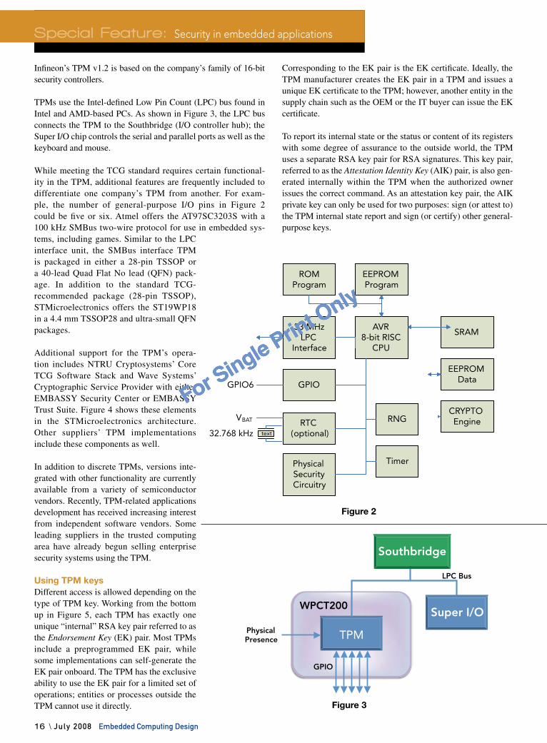
Available TPMsCompanies that develop MCU-based TPMs include Winbond Electronics, STMicroelectronics, Infineon Technologies, and Atmel. As shown in Figure 1, the microcontroller is typically packaged in an industry-standard 28-pin Thin-Shrink Small Outline Package (TSSOP). Atmel, which developed the first TPM to meet the TCG specification, uses an AVR 8-bit RISC CPU in its TPM. Figure 2 (page 16) shows the block diagram of common components integrated in a TPM IC.
Another TPM that uses an 8-bit core is STMicroelectronics’ ST19WP18, which is based on an MCU from a family initially developed for smart card and other secure applications. In contrast,
Figure 1
For Single Print Only
16 \ July 2008 Embedded Computing Design
Special Feature: Security in embedded applications
Infineon’s TPM v1.2 is based on the company’s family of 16-bit security controllers.
TPMs use the Intel-defined Low Pin Count (LPC) bus found in Intel and AMD-based PCs. As shown in Figure 3, the LPC bus connects the TPM to the Southbridge (I/O controller hub); the Super I/O chip controls the serial and parallel ports as well as the keyboard and mouse.
While meeting the TCG standard requires certain functional-ity in the TPM, additional features are frequently included to differentiate one company’s TPM from another. For exam-ple, the number of general-purpose I/O pins in Figure 2 could be five or six. Atmel offers the AT97SC3203S with a 100 kHz SMBus two-wire protocol for use in embedded sys-tems, including games. Similar to the LPC interface unit, the SMBus interface TPM is packaged in either a 28-pin TSSOP or a 40-lead Quad Flat No lead (QFN) pack-age. In addition to the standard TCG-recommended package (28-pin TSSOP), STMicroelectronics offers the ST19WP18 in a 4.4 mm TSSOP28 and ultra-small QFN packages.
Additional support for the TPM’s opera-tion includes NTRU Cryptosystems’ Core TCG Software Stack and Wave Systems’ Cryptographic Service Provider with either EMBASSY Security Center or EMBASSY Trust Suite. Figure 4 shows these elements in the STMicroelectronics architecture. Other suppliers’ TPM implementations include these components as well.
In addition to discrete TPMs, versions inte-grated with other functionality are currently available from a variety of semiconductor vendors. Recently, TPM-related applications development has received increasing interest from independent software vendors. Some leading suppliers in the trusted computing area have already begun selling enterprise security systems using the TPM.
Using TPM keysDifferent access is allowed depending on the type of TPM key. Working from the bottom up in Figure 5, each TPM has exactly one unique “internal” RSA key pair referred to as the Endorsement Key (EK) pair. Most TPMs include a preprogrammed EK pair, while some implementations can self-generate the EK pair onboard. The TPM has the exclusive ability to use the EK pair for a limited set of operations; entities or processes outside the TPM cannot use it directly.
Corresponding to the EK pair is the EK certificate. Ideally, the TPM manufacturer creates the EK pair in a TPM and issues a unique EK certificate to the TPM; however, another entity in the supply chain such as the OEM or the IT buyer can issue the EK certificate.
To report its internal state or the status or content of its registers with some degree of assurance to the outside world, the TPM uses a separate RSA key pair for RSA signatures. This key pair, referred to as the Attestation Identity Key (AIK) pair, is also gen-erated internally within the TPM when the authorized owner issues the correct command. As an attestation key pair, the AIK private key can only be used for two purposes: sign (or attest to) the TPM internal state report and sign (or certify) other general-purpose keys.
ROMProgram
EEPROMProgram
33 MHzLPC
Interface
AVR8-bit RISC
CPU
GPIO
RTC(optional)
PhysicalSecurityCircuitry
SRAM
EEPROMData
CRYPTOEngineRNG
Timer
text
GPIO6
VBAT
32.768 kHz
Figure 2
WPCT200Super I/O
TPM
LPC Bus
PhysicalPresence
GPIO
Southbridge
Figure 3
For Single Print Only

Embedded Computing Design July 2008 / 17
For strong digital identity, the external world can use the AIK pair to identify one TPM from another. To guard the user’s pri-vacy on a platform with a TPM, a given TPM can generate and operate multiple AIK pairs at any time. This allows the user to direct the TPM to use different AIK pairs for different transac-tions, making it difficult for an eavesdropper to track and cor-relate transactions.
Corresponding to the AIK pair is the AIK certificate. An AIK certificate is only issued by an entity that can be trusted to view the EK certificate and not disclose its details. Such an entity is referred to as the Privacy Certificate Authority in trusted comput-ing terminology because it issues AIK certificates and maintains the privacy of the EK certificate information.
The TPM allows general-purpose RSA key pairs like those used for encryption and signing to be generated and used. A general- purpose key pair is considered a Certified Key (CK) when the private key is digitally signed by the AIK private key (a TPM-resident key). Depending on the TPM resources, any number of CK pairs is available.
Using the appropriate protocol, an external entity can verify that a given CK pair is TPM-resident. The ability to prove TPM-resident keys represents one of the TPM’s attractive features because a TPM-protected key is more difficult to steal or modify compared to a software-protected key. The provability feature allows a soft-ware application on a platform with a TPM to transact with an external entity and prove (to that external entity) that the keys it is using reside in the TPM and are operated by the TPM, thereby increasing that external entity’s trust.
To prove that a CK pair is TPM-resident, TCG has specified a special attestation extension for the X.509 v3 certificate standard. An X.509 v3 certificate carrying the TCG-specified attestation extension for a CK public key is referred to as a CK certificate. To support broad deployment and compatibility with existing certificate authority products and services, a certificate authority (compliant to the RFC3280 standard) does not need to view the EK certificate in order to issue the CK certificate.
Protecting entry pointsToday, worldwide testing to find vulnerabilities and the onslaught
Figure 4
Systemprocesses
Userprocesses
Wave
NTRU
Application 1 Application 1 Application 1
PKCS# 11CSP
MS CAPICSP
TSS Service Provider - TSP
TSS Core Services - TCS
TPM Device Driver Library - TDDL
TPM Device Driver - TDD
ST19WP16 + Embedded TPM Firmware
MemoryAbsentDriver -MAD
MemoryPresentDriver -MPD
TPM BIOSDrivers
CryptographicInfrastructure Interface
TSP Interface
TCS Interface
TDDL Interface
OS UserMode
OS KernelMode
Hardware andFirmware
Figure 5
For Single Print Only

18 \ July 2008 Embedded Computing Design
Special Feature: Security in embedded applications
of attacks by hackers and thieves continually expose weaknesses in software, hardware, and overall protection strategies. In one recent report, researchers from Princeton University thought they discovered a weakness in the TPM when they froze a comput-er’s DRAM. On the contrary, the testing process itself made the system susceptible to attack.
Once decrypted keys are passed from the TPM to main system memory (DRAM), the keys might still be intact. Removing power from DRAM memory instead of suspending the system in a sleep mode provides an easily implemented strategy to avoid unauthor-ized access. This simply requires using the hibernate mode or shutting the computer down. However, the testing in this exam-ple demonstrated that improper use can reduce a security tool’s effectiveness.
When used properly, the TPM can add several higher-level security functions through its key and certificate capabilities. Recognizing the TPM’s potential to provide increased security, many companies are including the module in their products. Market research firm IDC anticipates that the TPM market will increase to more than 250 million units in 2010. If achieved, this equals an attach rate of more than 90 percent of all notebooks and desktops. Taking advantage of the TPM to establish strong device identity in locations that provide entry points to the
network, such as cell phones and PDAs, will add further protec-tion and close the back doors to hackers and thieves.
Thomas Hardjono is Principal Scientist at Wave Systems Corporation, based in Lee, Massachusetts. Thomas has 15 years of experience in security, including roles as Principal Scientist and security architect at VeriSign, Inc. and Bay Networks, Inc. (Nortel Networks). In addition to writing
more than 50 technical papers and three books on security and cryptography, he has authored a number of key specifica-tions in various standards organizations, such as the Trusted Computing Group (TCG), Internet Engineering Task Force (IETF), and Organization for the Advancement of Structured Information Standards (OASIS). Thomas has a PhD in Com-puter Science from the University of New South Wales and a BS (Honors) in Computer Science from the University of Sydney.
Wave Systems [email protected]
For Single Print Only

Security in embedded applications
20 \ July 2008 Embedded Computing Design
Specia
l Featu
re
FPGAs with built-in AES: The key to secure system designsBy Altera Technical Staff
FPGAs that conform to the National Institute of Standards and Technology (NIST) Federal Information Processing Standard (FIPS) 197 support configu-ration bitstream encryption using the 256-bit Advanced Encryption Standard (AES) and a nonvolatile key. AES is the most advanced encryption algorithm available today. A user-defined AES key can be programmed into the 256-bit non-volatile key stored in an FPGA device.
Choosing the correct encryption algorithm and selecting the appropriate key storage are two important design considerations. AES supports key sizes of 128, 192, and 256 bits and replaces the Data Encryption Standard (DES), which has 56-bit key and 64-bit data block sizes. Larger key sizes like AES equate to increased security and encrypt data faster than Triple DES (3DES). In effect, 3DES encrypts a docu-ment three times with three keys.
Encryption converts electronic data into an unintelligible form commonly referred to as ciphertext; decrypting the ciphertext converts data back into its original form or plaintext. The AES algorithm is a symmet-ric block cipher that encrypts/enciphers
and decrypts/deciphers electronic data in 128-bit blocks. In this algorithm, sym-metric keys are used for both encryp-tion and decryption, and the block cipher processes data in blocks. Symmetric key block cipher encryption algorithms are used in many industries because they provide high security protection and effi-ciency, ease of implementation, and fast data processing speed.
The choice of key storage is the second most important design consideration. The key is stored in either volatile or non-volatile storage, depending on the chip vendor. Once power for volatile storage is off, the key is lost unless an exter-nal battery is connected to the chip as a backup power supply. On the other hand, nonvolatile key storage gives the designer greater flexibility.
For example, the embedded nonvolatile key in an FPGA can be programmed either on or off-board. The security key is stored in poly fuses inside the FPGA. Poly fuses are nonvolatile and one-time programmable, meaning this storage approach is more reliable because no external backup battery is needed.
Poor reliability is the biggest problem bat-teries pose for volatile storage. Battery life is affected by temperature and moisture levels. When the battery dies, the key is lost. As a result, the device can no longer be configured, and the equipment must be returned to the vendor for repairs and key reloading. Also, battery backup cost is higher because it is more difficult to manu-facture, requiring more components, board space, and engineering work.
Batteries usually cannot stand the high temperature reflow process and must be soldered onto the board afterwards, which incurs an additional manufacturing step. Volatile key storage also requires the key to be programmed into the device after it is soldered on the board.
Because nonvolatile storage is one-time programmable, the key is tamperproof. That’s not possible in volatile storage because the battery can be removed and the FPGA can be configured with a regu-lar encrypted configuration file.
Designing security into a systemFigure 1 shows how security is imple-mented in Altera’s Stratix III FPGA using
Embedded systems can easily fall prey to hackers, security breaches, and malicious attacks
unless effective security is incorporated into the system design. Security is an even greater
issue today because new, proprietary technologies and valuable IP are used as competitive
barriers. Up until now, the technology for implementing conventional security has been
cumbersome, outdated, and costly. However, current trends are encouraging designers to
embed the highest level of security in FPGAs for more efficient and less costly designs.
For Single Print Only

Quartus II design software. The first step is programming the security key into the FPGA. The design software requires 256-bit user-defined keys (Key 1 and Key 2) to generate a key programming file. Then the file with the information from Key 1 and Key 2 is loaded into the FPGA through the JTAG interface.
Next, the AES encryption engine built into the FPGA generates the real key used to decrypt configuration data later in step three. The real key, created by encrypting Key 1 and Key 2, is then processed by a proprietary function before being stored in the 256-bit nonvolatile key storage.
In step two, the configuration file is encrypted and stored in external mem-ory. The design software requires the two 256-bit keys (Key 1 and Key 2) to encrypt the configuration file. The Quartus II AES encryption engine generates the real key by encrypting Key 1 with Key 2. The real key is used to encrypt the con-figuration file, which is then loaded into external memory, such as a configuration or flash device.
Thirdly, the FPGA is configured. At sys-tem power-up, the external memory device
sends the encrypted configuration file to the FPGA. The 256-bit nonvolatile key in the FPGA is processed by the inverse of the proprietary function to generate the real key. The AES decryption engine then uses the real key to decrypt the configura-tion file and configure itself.
Security break-insAs part of the design process, system designers must identify and understand the different types of security breaches, including copying, reverse engineering, and tampering, as shown in Table 1.
Copying involves making identical copies of a design without understanding how it works. Copying can be accomplished by either reading the design out of the memory device or capturing the configu-ration file when it is sent from the memory device to the FPGA at power-up. The sto-len design can then be used to configure other FPGAs. This approach constitutes a primary form of IP theft and can lead to significant revenue loss.
Reverse engineering entails analyzing the configuration file to re-create the origi-nal design at the register transfer level or in schematic form. The re-created design
Concerns Attacks
Copying
Black box attackReadback attackConfiguration bitstream probingProgramming state probing
Reverse engineeringReverse-engineering deviceReverse-engineering configuration bitstream
Tampering Reprogramming
Table 1
Config File
FPGA
Design Software
Key 1Key 2
Key 1Key 2
Real Key
Real Key
Real Key
Memory orConfiguration
Device
Key ProgrammingFile Generator
AES Encryptor
AES Encryptor
Function
Function-1
256-bit KeyStorage
AES Encryptor
AES Decryptor
Figure 1
For Single Print Only

22 \ July 2008 Embedded Computing Design
Special Feature: Security in embedded applications
can then be modified to gain a competi-tive edge. This is a more complex form of IP theft than copying and usually requires significant technical expertise. It is also time- and resource-intensive and some-times requires more work than creating a design from scratch.
Tampering involves modifying the design stored in the device or replacing it with a different design. The tampered device might contain harmful design code capa-ble of causing a system to malfunction or steal sensitive data.
Most nonvolatile FPGAs have a feature that permits configuration data to be read back for debugging purposes, as shown in Figure 2. Designers can usually set secu-rity bits for the device. When security bits are not set, readback is allowed and obtaining configuration data is straight-forward. But when security bits are set, readback is disabled. One way to conduct a readback attack when security bits are set is to detect where security bits are located in the FPGA and deactivate them to enable readback.
Setting up intrusion barriersSome FPGAs make it virtually impos-sible for attackers to steal IP from highly secured embedded designs. In particular, detecting and deactivating security bits can be difficult, thus providing designers greater defense against copying. The fol-lowing discussion explains how designers can set up those security defenses.
Poly fuses storing the security keys are hidden under layers of metal among hundreds of other poly fuses. It is nearly impossible to determine a particular fuse’s functionality by simple visual inspection. The programming status of the poly fuses used for other functions can be different from device to device.
This randomness makes it more difficult to identify which fuses store the security key. Also, even if the poly fuses storing the security key are identified, the real key used for decryption is not revealed because it is processed by the proprietary function prior to storage. Without knowing the real key, the design cannot be decrypted.
These FPGAs are thus secure against readback attacks because they do not support configuration file readback. This prevents attempts to read back the con-figuration file after it is decrypted within the FPGA. Furthermore, these designs cannot be copied by programming the security key into another FPGA and con-figuring it with an encrypted configura-tion file. Two 256-bit keys are required to program the security key into the FPGA. Because AES is used to generate the real key, it is virtually impossible to generate Key 1 and Key 2 from the security key.
Reverse-engineering a design from the configuration file is difficult and time-consuming as well, even without encryption. The FPGA configuration file contains millions of bits, and the con-figuration file formats are proprietary and confidential. To reverse-engineer a design requires reverse-engineering the FPGA or design software being used to reveal the mapping from the configuration file to the device resources.
Reverse-engineering these FPGAs is more difficult than reverse-engineering ASICs. Standard tools are not readily available to reverse-engineer these FPGAs, which are manufactured on a 65 nm advanced process technology node. In fact, reverse-engineering just one FPGA logic block can take a significant amount of time and resources. Configuration bitstream encryp-tion makes reverse engineering even more challenging. Finding the security
key to decrypt the configuration file is as complicated as copying it; thus, it might be easier and quicker to create a competi-tive design from scratch than attempt to reverse-engineer a secured FPGA design such as this.
Nonvolatile keys are one-time program-mable to guard against tampering. After the FPGA is programmed with the key, it can only be configured with configu-ration files encrypted with the same key. Attempts to configure the FPGA with an unencrypted configuration file or a config-uration file encrypted with the wrong key result in configuration failure. A configu-ration failure signals possible tampering, whether in the design’s external memory during transmission between the external memory and the FPGA or during remotely communicated system upgrades.
Design option comparisonsBesides the aforementioned FPGA secu-rity system, other design options avail-able to designers include SRAM-based FPGAs limited to 3DES encryption, flash-based FPGAs, and antifuse-based FPGAs. Table 2 describes the cost of attacks in each case.
Nonvolatile FPGAs retain their con-figurations when the power is off. One way to reveal device configuration is to probe or detect each nonvolatile cell’s programmable state. Two side-channel attacks on a flash-based FPGA are elec-tron emission detection and transistor threshold voltage change.
An attack via electron emission detection first involves removing the device’s pack-age to expose the die. Next, the device is placed in a vacuum chamber and powered up. The attacker then uses a transmission electron microscope to detect and display emissions. As for the second technique, a transistor’s threshold voltage changes over time because of electron accumulation in the floating gate. This causes the transis-tor’s threshold voltage to rise gradually.
In addition to these two side-channel attacks, another popular version, the power attack, involves measuring an FPGA’s power consumption to determine which function the device is performing. As for Figure 2
Readback Configuration Data
… 01101000001110010 … Nonvolatile
ReprogrammableFPGASecurity Bits
For Single Print Only

a readback attack on flash-based FPGAs, the amount of effort required varies from vendor to vendor and depends on how well security bits are protected in the device. Moreover, probing each flash-based FPGA’s floating gate takes a great deal of time and effort because the gate does not physically change after programming. The state, which is isolated by oxide, is determined by the existence or amount of electrons on the floating gate between the select gate and substrate (see Figure 3).
Furthermore, reverse-engineering a flash FPGA configuration file is not easy because the configuration file must first be obtained. This is a difficult task to accom-plish because the attacker must perform copying before reverse engineering. It is also important for designers to know that tampering with a flash-based FPGA is easy because the device is reprogramma-ble. A tamperproof mechanism therefore must be used if tampering is a concern.
Programming state probing is also used for attacking antifuse-based FPGAs. Techniques include Focused Ion Beam (FIB) technology and Scanning Electron
Microscope (SEM). FIB is used for micro-scope imaging and cross-sectioning the device, while SEM involves microscope imaging using raster-type scanning to detect secondary electrons emitted from the surface. Analyzing an antifuse-based FPGA’s programming state is extremely time-consuming, given the millions of antifuse links and the small percentage programmed.
Improved risk management strategiesDesigners must estimate total security costs and make trade-offs to determine the level of security that is right for the device under design. To achieve a high level of security, designers must analyze potential threats, consider the probability of attack given a particular set of vulnerabilities, and set up effective and appropriate defenses. FPGAs offer several reliable security schemes that enable designers to implement less costly strategies for managing risks.
Altera [email protected]
Select GateFloating
Gate Oxide
DrainSource
Substrate
Erase(Remove Electrons)
Program(Inject Electrons) e-
Figure 3
Attack typeFlash-based
FPGAsAntifuse-based
FPGAsSRAM-based
FPGAs
SRAM FPGAs with on-chip configuration
Readback attack Medium Medium - Medium
Programming state probing
Medium to high High - Medium
Reverse-engineering configuration data
Medium to high Medium to high High Medium to high
Device reprogramming
Low - Low Low
Table 2
For Single Print Only

24 \ July 2008 Embedded Computing Design
Designing with EDA and virtual simulation toolsSoftw
are
Electronic Design Automation (EDA) flows are built on the fundamental prem-ise that models are interoperable and freely interchangeable among vendors, meaning that models can be written or obtained from anywhere and be accepted by any vendor’s tools. These features have been elusive for the abstract models nec-essary to support high-performance pro-totypes. Because of this, EDA has failed to deliver a system-level virtual prototype that provides the right levels of capability and speed of execution.
Major changes happening in both the hardware and software worlds will soon make it impossible to construct systems without an abstract model. By adopt-ing reuse, designers are now essentially assembling complex embedded systems like LEGO systems. Processor complex-ity has hit a wall created by diminishing performance gains at the expense of huge power increases, such that most systems today utilize multiple heterogeneous
processors rather than one central proces-sor. As system functionality continues to grow, it must cope with the transition to a multiprocessor world. With all of these changes, designers cannot continue build-ing systems without a viable system-level model on which this functionality and architecture can be designed and verified.
Historical perspectiveHardware/software coverificationSome companies have attempted to bring the hardware and software communities together by providing virtual hardware models that can be used for software development. For example, Seamless from Mentor Graphics substituted Instruction Set Simulator (ISS) models for each processor and integrated them into a conventional Register Transfer Level (RTL) simulation environment[1]. This model aided driver debugging but lacked sufficient performance for any-thing else. The Seamless product also included several performance boosters
that virtualized the host memory system, which extended its usage into some low-level operating system areas[2].
In later years, faster models replaced the RTL models, such as C or SystemC mod-els[3]. Although these models provided better performance, complex systems still operated too slowly, making them unsuit-able for mainstream software usage.
SystemC prototypesThe industry has spent considerable time and effort constructing virtual platforms based on SystemC. Examples include platforms created and proliferated by CoWare[4] and the proposed work proj-ect under the Eclipse Virtual Prototyping Platform (VPP)[5]. These prototypes pro-vide a flexible and adaptable platform on which bus traffic, power, performance, and many other implementation attributes can be analyzed. While much faster than the RTL prototypes discussed, these pro-totypes perform at levels that keep them
OVP makes system level virtual prototyping a realityBy Brian Bailey
As software content continues to grow in importance and
complexity, the industry is facing challenges presented
by multiple heterogeneous processors with much tighter
communications than in the past. To ensure quick time to market for high-quality software,
developers need a high-performance, system-level virtual prototype of the hardware, on which
software can be designed, implemented, and tested. While previous prototypes have been
too slow or arrived too late in the development cycle, the recently announced Open Virtual
Platforms (OVP) initiative enables both early and fast virtual prototype availability.
Ph
oto
cou
rtes
y of
LE
GO
For Single Print Only

in the domains of hardware verification and firmware development.
In addition, SystemC has failed to solve the model interoperability problem, an issue that the Open SystemC Initiative (OSCI) Transaction-Level Modeling (TLM) group is trying to rectify. The group’s lat-est attempt has not impressed many in the industry, as some have called the effort “too little too late.” Furthermore, this pro-posed standard only addresses memory-mapped interfaces, limiting its ability to define a complete system-level prototype.
Other companies such as Virtutech and VaST Systems[6] have forsaken the stan-dards arena and used custom languages and tools to create faster models of pro-cessors, memory systems, and some aspects of hardware. While these compa-nies have successfully created prototypes with higher performance, they suffer from the problems of model availability and proprietary formats.
Changing needs and increasing complexityMost prototypes today include timing, which is essential for hardware and archi-tecture verification as well as low-level driver testing. But timing information slows down the prototype. For the soft-ware team handling applications devel-opment, timing information is unneces-sary. Time advances as each processor is clocked, and events advance in the correct order for each thread.
To work reliably, multiprocessor applica-tions must perform synchronization that does not depend on timing. Thus, a system-level model for the software community can dispense with timing altogether, rely-ing instead on sequential order of execu-tion and proper synchronization between threads. Synchronization is performed using semaphores, handshakes, or other mechanisms that ensure the two software threads that need to communicate are both in the necessary state for exchanging data.
As time progresses, developers are not as concerned about how a single block or an isolated algorithm functions as they are about controlling and coordinating blocks and algorithms to form a complete
For Single Print Only
26 \ July 2008 Embedded Computing Design
Software: Designing with EDA and virtual simulation tools
multifunction system. This additional capability leads to increased complexity. Total system complexity is proportional to the square of the number of independent nodes that communicate. These nodes can communicate with each other and col-laborate to perform the total function. By implication, each of those nodes performs an independent task or coordinates with others to fulfill a more complex task. With the advent of multiprocessor Systems- on-Chip (SoCs), software has now become truly multinodal because threads can execute in a fully concurrent manner and interact with each other in real time.
Multiprocessor software demandsIn the past, cross-compiling the code onto the host was quick and easy; however, this does not hold true for multiprocessor soft-ware. Even though current desktops now have two or four processors, they provide a less reliable view into how software will operate or perform on the actual embed-ded hardware, which might have special communications between the processors or require heterogeneous processors. Mul-tiprocessor software needs a more accurate prototype to investigate application com-munications and synchronization.
At the other end of the scale, many com-panies utilize physical prototypes to con-duct software verification. While these prototypes operate at near real-time speeds and have accurate timing, they are available too late in the develop-ment cycle, given that problems found in the software cannot be reflected by
necessary changes in the hardware. With the introduction of multiprocessor systems, it is more difficult to see what each processor is doing in real time, and operations such as single-stepping are almost impossible. Designers need a plat-form that provides the same level of per-formance but is available earlier in the design cycle.
OVP overviewOSCI maintains the SystemC language and provides a free simulator. While these offerings appear beneficial, they have in fact stifled commercial advancements. In addition, SystemC has failed to solve the model interoperability problem discussed earlier.
Imperas recently launched the OVP initiative to promote the open virtual platform concept. OVP encourages developers to adopt the new way of developing embedded software, especially for SoC and multiprocessor SoC plat-forms. The company took a different approach with OVP and OVPsim by first making the interface available to the public, thus addressing the model interoperability prob-lem. The company offers sev-eral models that demonstrate the interface’s capabilities as well as a Windows platform simulator for developers to build and debug models.
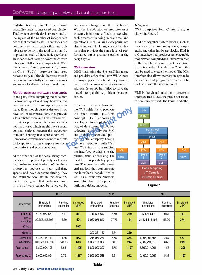
InterfacesOVP comprises four C interfaces, as shown in Figure 1.
ICM ties together system blocks, such as processors, memory subsystems, periph-erals, and other hardware blocks. ICM is a C interface that produces an executable model when compiled and linked with each of the models and some object files. Given that it is standard C code, any C compiler can be used to create the model. The ICM interface also allows memory images to be defined so that programs or data can be preloaded into the system model.
VMI is the virtual machine or processor interface that allows the processor model to communicate with the kernel and other
Beh
BHM
BHM
Peripheral Model
PPM
ICM ICM
ICM ICM ICM ICM
Mem Proc
1 Proc
2 Mem
VMI VMI
Code Morphing
JIT Compiler
Simulation Kernel
Figure 1
OR1K ARM MIPS
Benchmark Simulatedinstructions
Runtime (seconds)
Simulated MIPS
Simulatedinstructions
Runtime (seconds)
Simulated MIPS
Simulatedinstructions
Runtime (seconds)
Simulated MIPS
LINPACK 5,783,952,671 13.11 441 1,110,694,547 3.70 299 97,571,640 0.51 191H.264
encoding 20,655,155,698 48.60 424 6,967,978,843 37.76 184 21,324,418,192 56.99 374
uClinux 395*
Queens 1,303,321,123 4.84 269
Dhrystone 6,498,118,119 14.36 453 1,214,070,280 3.75 324 1,096,094,508 2.57 427Whetstone 140,023,166,816 228.36 613 8,084,138,084 33.06 244 2,589,794,515 8.65 299
Peak speed 1 6,800,004,105 5.68 1,195 5,600,003,303 4.75 1,177 5,600,014,901 4.55 1,228
Peak speed 2 7,600,010,964 5.76 1,317 7,600,003,529 8.31 912 6,400,015,068 5.37 1,187
Table 1
For Single Print Only

components. VMI is essentially the heart of the high-performance execution pro-vided by OVP. OVP uses a code-morphing approach with a just-in-time compiler to map the processor instructions into those provided by the host machine. In between is a set of optimized opcodes into which the processor operations are mapped. OVPsim provides interpretation or com-pilation into the native machine capabili-ties. This differs from the traditional ISS approach, which interprets every instruc-tion. VMI also enables a form of virtu-alization for capabilities such as file I/O, which allows direct execution on the host using the standards libraries provided.
PPM, the peripheral modeling interface, is similar to the fourth interface, BHM, which is intended for more generalized behaviors. These models run in a second portion of the simulator called the Periph-eral Simulation Engine. OVPworld states that “this is a protected runtime environ-ment that cannot crash the simulator.” It does this by creating a separate address space for each model and restricting com-munications to the mechanism provided by the API. The principal difference between the two interfaces is that the PPM interface understands buses and net-works. It is thus similar to the OSCI TLM interface proposal in terms of functional-ity. The BHM more closely resembles a traditional behavioral modeling language with process activation and the ability to wait for time or a specific event.
Performance benchmarksSeveral different processor models and prepackaged demos are available at the OVPworld website (http://ovpworld.org). A free simulator is available for develop-ers to create their own platforms. Table 1 shows the performance results obtained for each of the cores running various benchmarks.
The cornerstone of hardware/software virtual prototypesOVP has the potential to provide a true system-level virtual prototype for both hardware and software development. It is poised to become the first general- purpose abstract modeling system that will form the cornerstone of complete flows into the hardware and software
communities. While this has been accom-plished before in specialized areas such as DSP designs, it has never been solved in the more general case. OVP has enabled the commercial market for these proto-types, meaning that it could garner more commercial attention than SystemC. If successful, OVP will address the model interoperability problem and thus benefit the entire industry.
Brian Bailey is an in-dependent consultant for ESL, verification, and system design companies, such as Imperas. Previously, he worked at Mentor Graphics for 12 years
in roles such as chief technologist for verification. Brian, who has published four books and several technical pa-pers, graduated from Brunel University in England with a first class honours degree in Electrical and Electronic Engineering.
1.800.665.5600www.tri-m.com [email protected]
tel: 604.945.9565 fax: 604.945.9566HEAD OFFICE: VANCOUVER
100Mhz PC/104 Module
Featuring the new edition ZFx86FailSafe® Embedded PC-on-a-Chip
Dual watchdog timers, PhoenixBIOS and FAILSAFE Boot ROM
Extended temperature -40°C to 85°C
MZ104
75 Watt High Efficiency PC/104
The VT104 VersaTainer is a rugged aluminumenclosure that can be used as either a PC/104,
PC/104+ or EBX enclosure.
The solid one-piece extruded body provides dualinternal shock and vibration protection.
PC/104 VersaTainer
75 Watt output
+5V, +12V, -12V outputs
6V to 40V Dc input range
PC/104 compliant
VT-104
HE104-75W
ReferencesKlein, Russ. “Hardware Software co-[1] verification.” Mentor Graphics white paper. www.mentor.com/products/fv/techpubsHarris, David; Stokes, DeVerl; and Klein, [2] Russ. “Executing an RTOS on simulated hardware using co-verification.” Mentor Graphics white paper. www.mentor.com/products/fv/techpubsAndrews, Mike. “Managing design [3] complexity through high-level C-model verification.” Mentor Graphics white paper. www.mentor.com/products/fv/techpubsSerughetti, Marc. “Virtual Platforms [4] for Software Development – Adapting to the Changing Face of Software Development.” CoWare white paper. www.coware.com/news/techpapers.phpEclipse Virtual Prototyping Platform [5] (VPP) – www.eclipse.org/proposals/vppHellestrand, Graham. “Systems [6] Architecture: The Empirical Way – Abstract Architectures to ‘Optimal’ Systems.” VaST white paper. www.vastsystems.com/docs/EmpiricalSystemsArchitecture 20050722Pub.pdf
For Single Print Only

28 \ July 2008 Embedded Computing Design
Designing with EDA and virtual simulation toolsSoftw
are
Modeling techniques maximize value of virtual platformsBy Andy Ladd
Over the past several years, development teams and methodology groups have placed greater emphasis on platform-driven design techniques. Shorter product life cycles and heightened time-to-market pressures have forced companies to invest in system-level platforms available earlier in the design cycle. In addition, the tran-sition to System-on-Chip (SoC) design techniques leveraging legacy and third-party IP has provided better structure and methodology for modeling at the system level. Meanwhile, the increasing amount of embedded software and firmware content has repositioned the majority of resources required to produce a product into the software domain. In a traditional design flow, this means a larger portion of the development process is shifted later in the design flow, increasing schedule risk.
Virtual platforms help address these ever-increasing complexity issues, mar-ket pressures, and changes in content. Although some engineers have described the benefits of these platforms in detail, identifying appropriate modeling meth-ods is usually left as an exercise for the reader. To shed some light on this facet of virtual platforms, the following dis-cussion will analyze different aspects of proper modeling techniques.
Ironically, while models provide the back-bone for any system-level platform, the difficulties and expenses associated with developing these models have limited virtual platform adoption. In addition, modeling and support efforts consume the lion’s share of the costs for develop-ing and supporting these platforms.
Model abstraction levelsFor this discussion, models can be par-titioned into four distinct parts: timing, functionality, addressable state, and inter-faces. Each of the model’s four parts can vary at different abstraction levels, from high-level behavioral descriptions to the actual design implementation. Models cre-ated directly from design descriptions that reflect true design behavior are referred to as implementation-accurate models. The modeling stack in Table 1 shows the con-tinuum of abstractions between the high-est and lowest extremes.
As with most applications related to com-puting, increasing accuracy has a direct impact on reducing execution speed. This
is no different with modeling; boosting a model’s accuracy requires more process-ing and a reduction in execution speed.
In addition, increasing model accuracy directly correlates to the amount of effort and time required to create and support models. Finding the proper speed versus accuracy trade-off is paramount to achiev-ing a modeling paradigm that will meet virtual platform users’ needs and limit the amount of effort required to develop and maintain the platform.
At one end of the spectrum, hardware engineers need implementation-accurate models to validate their designs. At the other end, application software developers
System-level environments increase developer productivity
and bring products to market earlier, providing a
development platform for architectural analysis, hardware/
software codevelopment, and system validation. Models
provide the backbone for any system-level platform;
however, the difficulties and expenses involved in
developing these models have limited virtual platform
adoption. Andy describes the importance of an effective
modeling strategy for virtual platform development.
Abstraction Common names
Behavioral Programmer’s View (PV), Untimed (UT)
TimedPVT, Loosely Timed (LT), Approximately Timed (AT), cycle approximate
Cycle Accurate Clock Accurate (CA)
Implementation AccurateRegister Transfer Level (RTL), Design Simulation Model (DSM)
Highest
LowestTable 1
For Single Print Only

can get by with high-level behavioral mod-els. Between these two extremes lie lower levels of software, including the Operating System (OS), driver, firmware, and archi-tectural and performance analyses.
Application software engineers are most concerned about developing their applica-tions and having a productive debug envi-ronment. They don’t need the accuracy of a detailed model; their code rarely touches the actual hardware because it’s layered on other software. However, application soft-ware engineers in some cases might need to understand simple performance metrics that require more accuracy.
Unlike application code, OS and driver development touches the hardware; thus, those who develop these components need a higher degree of accuracy to understand how their software and the underlying hard-ware interact. They can exchange speed for higher accuracy because their code base is smaller than application software engineers’ code base. Untimed behavioral models might be useful for early develop-ment, but ultimately, OS and driver devel-opers must understand how their software works using more accurate models to ensure that the whole system (hardware and software) will work together.
Firmware engineers develop code – boot code, self-test, diagnostics, and console – that interacts with hardware. Given this high level of interaction with and dependency on hardware, these engineers have little use for inaccurate models. They can swap model speed for higher accuracy because their soft-ware is at the lowest level and is usually small compared to that of higher levels. Tuning low-level firmware and driver software performance also requires cycle-accurate models to understand timing dependencies on hardware as well as resource bottlenecks.
Architects need to know how their hard-ware/software partitioning, IP selection, bus architecture, memory architecture, and overall architectural decisions impact the system as they relate to performance, area, and power. They also must under-stand pipeline effects, latencies, through-put, bandwidth, and activity. A final design
For Single Print Only

30 \ July 2008 Embedded Computing Design
Software: Designing with EDA and virtual simulation tools
that doesn’t perform as architects planned could dramatically affect the product’s cost, performance, and schedule. There-fore, architects must validate their designs using highly accurate models that build confidence in their decisions. Hardware engineers must have implementation-accurate models; any other level of accu-racy is unsuitable for validating designs.
A single abstraction level for all models is not always appropriate in every case. For example, an architect considering memory architecture trade-offs might try to analyze each prospective memory sub-system’s memory latency and throughput. In this case, architects might need highly accurate models for memory controllers and memory interfaces to ensure that they fully understand the performance. The rest of the system can be modeled at more abstract levels because it isn’t critical to the analysis. Using a model methodology that supports mixing abstraction levels and enables plug-and-play for models of dif-ferent abstraction levels can help optimize execution speed and analysis accuracy.
Finally, when considering all possible use cases, engineers should note that a plat-form rarely targets only one type of user. It is more common that a virtual platform will be created to address the needs of many types of users, ranging from soft-ware developers to architects and, in some cases, hardware designers. There-fore, different abstraction levels must be supported within the platform.
Interoperability and compatibilityWhen creating a modeling methodol-ogy, developers should make sure models are interoperable with each other, spread across abstraction layers, and compatible with various platforms and third-party tools. Consistency is also important to guarantee that models created by differ-ent model developers are compatible with each other.
Though not perfect, standards help add consistency, compatibility, and interop-erability among models by supporting various model abstractions and providing compatibility with different platforms and third-party tools.
Modeling languages such as SystemC pro-vide a base platform to connect and exe-cute different models. SystemC provides the flexibility to support multiple abstrac-tion levels and communication interfaces. Combining SystemC with interface stan-dards, such as the proposed Transaction-Level Modeling (TLM) 2.0 specification in development by the Open SystemC Initiative (OSCI), provides an environment that maintains compatibility with various modeling elements and abstractions and makes them interoperable with each other and other platforms.
In addition, when refining models from different abstraction levels, develop-ers should reuse as much information as possible from one model to another and reuse modeling information from one revision of an IP block to another. Consistent methodology and standards provide the mechanisms to accomplish these tasks. Developers also can reuse interfaces, state access mechanisms, and timing from one model to another. Stan-dards such as Spirit IP-XACT, the IP metadata specification from the SPIRIT Consortium, can help developers import and export configuration information and check differences between model revi-sions and abstractions.
A modeling methodology that doesn’t guarantee interoperability among differ-ent models and abstractions or provide compatibility with other platforms and third-party tools is ill suited for most proj-ects. In fact, lack of interoperability and compatibility has slowed virtual platform adoption within the embedded industry.
Meeting supply chain needsThe growing need for providing models across the supply chain reinforces the importance of interoperability, compat-ibility, and standards. IP providers must supply early models of their IP because customers need the ability to select the appropriate IP for their products. Without proper models, customers have no way of knowing what IP will work best in their systems. Customers also need a platform for their own development (architecture, hardware, and software) to hit their mar-ket window with the correct product.
Any modeling methodology that sup-ports IP delivery across the supply chain must take this into consideration. IP must be compatible with end customers’ plat-forms and models, yet at the same time provide security and be impervious to reverse engineering.
Breaking down modeling barriersA well thought-out modeling methodol-ogy can overcome obstacles to virtual platform adoption as well as ensure that users attain all the value that a virtual platform can provide. Virtual platform modeling should support models of vari-ous abstraction levels, model plug-and-play, and standards for interoperability, compatibility, and reuse.
The industry needs to provide tools that automatically support model generation in a consistent manner across the vari-ous abstraction levels. These tools must incorporate standards and preserve the investment that developers put into their models. Requirements should:
Make the model developer more fproductiveReuse information from legacy fmodels or models of different abstractions levelsSupport standards to ensure finteroperability and a migration path for models to other virtual platformsProvide consistency checks to validate fmodels across abstraction levelsOffer configuration management and frevision control aid for model support and distribution
Andy Ladd is VP of applications and methodology at Acton, Massachusetts-based Carbon Design Systems, Inc., where he is responsible for
providing and supporting automatic system-level modeling and validation solutions.
Carbon Design Systems978-264-7300aladd@carbondesignsystems.comwww.carbondesignsystems.com
For Single Print Only

32 \ July 2008 Embedded Computing Design
UNITUNDERTEST
New LXI standards in development: It’s about your time
By David Owen, Bob Stasonis, and Elizabeth Persico
The LXI standard identifies three functional certification classes: Class C, Class B, and Class A. The class succession from C to A provides progressively more functionality and gives instrument designers the ability to incorporate the precise functionality required for their instruments and intended applications.
Classes of LXI productsFunctional Class C LXI Devices provide a standardized LAN and Web browser interface conformant with the LXI standard. These devices, which are not required to support either the wired trigger or IEEE 1588 timing aspects, are particularly suited to applications where non-LXI products have been adapted to the standard. This class includes physically small products (such as sensors) that use battery power or Power over Ethernet and devices with key attributes including a simple architecture, low cost, and small size.
Functional Class B LXI Devices provide a standardized LAN interface, synchronization API, and IEEE 1588 timing support. The Class B interface allows devices to execute triggered func-tions equivalent to those available over the General-Purpose Interface Bus (GPIB) with similar or better timing accuracy.
Functional Class A LXI Devices provide a standardized LAN interface, synchronization API, IEEE 1588 operation, and a wired trigger bus interface. The wired trigger bus provides a standard-ized capability for supporting trigger events between devices whose timing accuracy is limited by cables and LXI Device hard-ware. The trigger functionality is broadly equivalent to the back-plane triggers of modular instruments in card cages (though cable lengths might be longer than backplane trigger lengths) and the ad hoc point-to-point trigger systems used on bench instruments.
Since the release of the LXI standard, most instruments have been certified as Class C. These instruments incorporate the key fea-tures attributed to LXI-compliant instruments, built-in Web servers so that users can monitor and control the system using Ethernet, and any standard Web browser. All major instrument function-alities are accessible through the Web server, which simplifies
software development, system commissioning, troubleshooting, and maintenance. Some of these Class C instruments include fea-tures associated with Class B or Class A LXI Devices but not the complete set of features required to declare class compliance.
Web services are used to gain access to LXI Devices and achieve immediate control over their configuration, making them easy to set up, configure, and debug. These LXI Devices allow users to build quick and easy-to-manage test systems that can be remotely controlled, as shown in Figure 1.
Figure 1
Class B to the frontThe Consortium is now witnessing the emergence of Class B instruments. Class B instruments provide LAN and Web server functionality with the addition of a synchronization API and sup-port for the IEEE 1588 precision time protocol. These features allow devices to execute trigger functions and, for the first time, standardize a method for executing triggers in a system based on knowledge of common system time reference to an accuracy not achievable before the advent of IEEE 1588.
Recent activities, including the rise of Functional Class B LXI instruments and the
LXI Consortium-sponsored PlugFest and LXI Day events, demonstrate how more vendors are
adopting the LXI standard and thus stimulating LXI system sales growth. As LXI compliance
becomes a key component in Ethernet-enabled systems, the LXI Consortium is focusing on
ways to improve compliance testing procedures for the standard.
EthernetConnectivity
Devices
For Single Print Only

Class B LXI Devices provide timing and synchronization between the various components based on a common reference clock without requiring a controller (PC) to be the origin of time information. The IEEE 1588 scheme ensures that instru-ments agree on the correct current time, leveraging a master clock located within the system. Even if the time “known” by the system is wrong relative to the physical world, instruments still agree on the timing and perform the various functions required in the correct sequence at the correct interval.
In addition to this feature, the LXI standard introduces time-based triggers. Prior to LXI, test and measurement instruments typically relied on PCs and an active Internet connection for the time check, which created opportunities for inaccuracy. IEEE 1588 timing is more accurate and consistent and can avoid the message-based triggers issued from a controller at time-sensitive moments. This controller and its operating system can cause variable delay in the trigger because of latency and variable delays. Windows-based controllers commonly cause several milliseconds of variable delay. Though Real-Time Operating Systems (RTOSs) can improve tim-ing variability by limiting latency, they still introduce uncertainty, and delays are still present.
LXI Devices can circumvent network and controller latency. A typical local LXI test system with IEEE 1588 capability using a hardware PHY is accurate to approximately 50 nanoseconds. The test system has access to additional capabilities including peer-to-peer triggering, which enables the instrument to respond to an instruction from another instrument, also circumventing any controllers or other components in the system.
Certifying a productTo certify an LXI product, the manufacturer must be a member of the LXI Consortium, which ensures access to the documenta-tion and support needed to guarantee the device meets all the requirements for conformance. The documents include forms that must be filled out and submitted to the Conformance Work-ing Group. The Consortium also supplies a suite of conformance pre-test software that allows manufacturers to check if products conform to the LXI standard.
Members ready to submit instruments for testing can attend a PlugFest or hire one of several approved private testing ser-vices. Either way, a representative from the manufacturer who is familiar with the instrument must be present during testing. Test results are forwarded to the LXI Conformance Working Group Chairperson, who then forwards the application to the Board of Directors with a recommendation. After the Board votes, the Consortium notifies the manufacturer and, if the application is denied, explains the reasons why and recommends ways to resolve the issues.
During a PlugFest, the Consortium pays an independent lab to perform conformance testing on members’ early designs. If prob-lems are found, experts are available to help vendors improve their implementations. Applications and tutorial sessions at PlugFests help new members and integrators become familiar with LXI.
3rd Annual Flash MemorySummit & Exhibition
August 12-14, 2008Santa Clara, California
Details & Registration Online:FlashMemorySummit.com
Exhibit Space & Sponsorship Information:[email protected]
“The NAND market has grown fasterthan any technology in the history of
semiconductors, becoming a $16billion market in 2007, less than a
decade after introduction.” — Jim Handy, Objective Analysis
Attend Flash Memory Summit for thelatest practical information on flashmemory and the most recent develop-ments in flash memory applications.
Learn to make your products
Fast, Rugged and Mobileat the only conference
dedicated to flash memory!
For Single Print Only

34 \ July 2008 Embedded Computing Design
UNITUNDERTEST
Focus on LXI and RF test systems
Future improvementsLAN is ubiquitous, and more test systems are using it. LXI puts the power of Ethernet and the Web inside those systems, allowing users to create the system needed today and quickly move on to the next one. Figure 2 shows the many application options for LXI.
Figure 2
The next revision (1.3) will incorporate IEEE 1588-2008 into the LXI standard. Future revisions will concentrate on enhancing how LXI products communicate directly with each other and the user. New feature sets will include:
Improved Web support for trigger operations, allowing users fto initiate and test trigger operation through Web pages without using the programmatic interfaceResource management, which allows users to more easily fmanage multicontroller systemsState management, which handles common functions like fstore and recallEvent log and schema, which improve how LXI devices log fevents and report them so that logs from different devices can be combined more easilyPeer-to-peer communication that does not rely on a controller f
This work will likely take a year to prototype, test, and document before it is included in Revision 2. In the next six months, the Consortium will take major steps toward improving compliance test procedures for the standard.
More member companies are commenting on how customers will not accept a non-LXI version of an Ethernet-enabled prod-uct, insisting instead on an LXI version. This is helping boost LXI instrument sales and encouraging new vendors to adopt the standard.
Furthermore, many customers are insisting on LXI as more sys-tems are developed with LXI compliance as a key component. LXI-enabled instrument sales are increasing rapidly, making LXI the fastest adoption ramp of any I/O architecture. While the numbers are still small as a percentage of the overall multibillion
dollar test and measurement industry, this is largely dictated by the amount of legacy equipment available and the long lead times for military programs. Nevertheless, LXI system sales are rising rapidly as more products are being introduced, and the Consor-tium expects that growth to continue.
Face to face in TorontoThis year’s PlugFest held May 21-23 in Toronto concentrated on testing the latest version of IEEE 1588-2008, slated to be incor-porated in the specification later this year. During this PlugFest, the Consortium developed formal test procedures and tested proposed rules that expand standards coverage for system-level aspects of LXI test systems. These issues included resource and state management in a multicontroller environment, event logs, and peer-to-peer communication issues. Face-to-face meetings with experts in each area complemented the test work.
Also in May, the Consortium hosted its first LXI Day open to the general test and measurement community. This special event provided working LXI product demonstrations and showcased technical application presentations that explained LXI’s benefits, its importance to the future of test and measurement, and ways it can be implemented in various applications.
The PlugFest held in Newport Beach earlier this year made prog-ress in testing IEEE 1588 and starting the process to incorporate 1588-2008 into the standard.
The LXI Consortium has an active Development Group that reviews developing LXI products. The Consortium invites speak-ers to address the group, which includes many vendors who are not members of the Consortium, to provide those defining the LXI standard with comprehensive, objective viewpoints. As with any network, the value of the network increases with the number of nodes. LXI recognizes this and invests resources in helping mem-bers, integrators, and product vendors ascend the learning curve.
The LXI Consortium provides a venue for LXI vendors to work together, even though the companies involved might be competi-tors. This benefits end users by allowing systems integrators, engineers, and developers to influence the standard’s develop-ment. LXI is a true multivendor standard in the sense that a vari-ety of vendors are motivated to grow the standard for the test and measurement industry.
David Owen is Technical Committee Chair for the LXI Consortium. Bob Stasonis and Elizabeth Persico are Marketing Committee cochairs for the LXI Consortium.
LXI [email protected]@pickeringtest.comelizabeth_persico@agilent.comwww.lxistandard.org
LXISwitching
LXIGeneral-Purpose
MeasuringInstruments
LXIPower
Supplies
LXISignal
Generators
LXIAnalyzers
LXIWTB
Accessories
LXIBridges
LXIEthernetNetwork
LXISynthetic
Instruments
For Single Print Only

Embedded Computing Design July 2008 / 35
UNITUNDERTEST
Designing the RF test
instruments of tomorrowBy Mark Elo
The demand for wireless communication continues to increase with the number of new users and services continually expand-ing. Moreover, wireless communication traffic is migrating from mostly voice to mostly data, requiring faster data rates.
With limited frequency spectrum, digital wireless technology has progressed rapidly during the past two decades to address these market demands. More spectrally efficient modulation types and digital coding schemes are being used along with increased signal bandwidths from 300 kHz in the early 1990s to 40 MHz today. New transmission methods such as MIMO are being deployed to further increase data rates. This next generation of RF test equip-ment adds more layers of complexity, thus posing difficulties for test engineers.
MIMO test equipment complications MIMO is a growing RF technology that uses multiple radios for both transmitting and receiving data. In wireless communication devices, it can increase data throughput rates or improve trans-mission quality without requiring additional bandwidth.
In a typical MIMO approach, four independent Orthogonal Fre-quency Division Multiplexing (OFDM) carriers are placed atop one another, as shown in Figure 1. This MIMO technique allows
transmitting up to 3.5x as much information in the same band-width as a single carrier.
Testing MIMO presents several key challenges, including the amount of spatial streams that can be supported. For example, Wireless LAN (WLAN) and Long-Term Evolution (LTE) both support four-stream configurations, and current WiMAX tech-nology with Matrix A and B configurations supports two streams. Another issue is keeping costs per stream down without sacrific-ing performance. Costs for test equipment, especially MIMO systems, can multiply quickly. For instance, to get N inputs and M outputs, each I/O requires a separate transmitter and receiver or source and analyzer.
Bandwidth poses an additional problem. MIMO signals in partic-ular require test instruments with wide bandwidths. For example, WiMAX and LTE have a current 20 MHz bandwidth requirement, and 802.11n WLAN has a 40 MHz bandwidth. Instrumentation must be able to perform these measurements while maintaining exceptional Error Vector Magnitude (EVM) performance.
High sensitivity is another critical parameter. The noise floor affects modulation accuracy, measured as the EVM. Higher noise will increase the EVM, reducing communication quality. With
wide signal bandwidths, low noise in both the signal generator and the signal analyzer is important. Low-cost instruments have poorer noise performance than their more expensive cousins, which directly affects measurement accuracy. This in turn weakens product quality and production yields, which impacts product cost and competitiveness.
MIMO relies on channel distortion. Without it, MIMO as a transmission technique becomes redundant. Understanding how devices per-form under different channel conditions and calculating those conditions with mea-surements such as Channel Response or the Matrix Condition are important capabilities. Take WLAN as an example. A header is transmitted with a known symbol pattern.
Testing modern RF systems takes … well, a modern RF system. New types of Software-Defined
Radio (SDR)-based test instruments are coming to the forefront with the technology needed to
test new transmission methods such as Multiple Input/Multiple Output (MIMO).
Figure 1
For Single Print Only

36 \ July 2008 Embedded Computing Design
UNITUNDERTEST
Focus on LXI and RF test systems
The receiver uses this known signal to reveal what the channel distortion looks like and then determines the actual received data symbols.
Measuring wide bandwidth OFDM signals’ channel response, that is, the amplitude and phase changes across the channel, poses another challenge. To accu-rately characterize a transceiver unit under test, the test equipment must not only have wide bandwidth but also flat response with low amplitude and phase variation.
Next-generation RF test instrument innovationsWith the next generation of MIMO, beam-forming appli-cations will become more prevalent. Second-generation MIMO test systems will require that the RF carrier phase and amplitude be accurately controlled. This enables the transmitters to produce different antenna patterns, allow-ing the antenna beam to be steered to different locations. Steering the antenna beam to each user increases commu-nications efficiency. Most of today’s instrument platforms were designed for Single Input/Single Output (SISO) applications and cannot easily control RF carrier phase.
Some MIMO test system architectures only support balanced MIMO configurations such as 2x2, 3x3, or 4x4. Future instru-mentation must also support unbalanced MIMO configurations, especially for collaborative MIMO such as 1x2, 2x3, and 3x4 configurations. As more advanced beam-forming applications come online, 8x8 and 16x16 configurations could be required.
Time alignment between transmitters and receivers is also criti-cal. As MIMO relies on time discrepancies in the channel to function correctly (multipath), timing misalignment within the signal analyzer or sources will result in increased distortion from the test instruments, reducing measurement accuracy.
Next-generation capabilities will rely on several unique industry innovations. For instance, a DSP-based SDR architecture adapts to the dynamic wireless market’s quickly changing test require-ments, giving the instrument added longevity by making it easily upgradeable. SDR-based instruments can generate or demodu-late virtually any signal with up to 40 MHz of modulation band-width, which is important for many of today’s devices and for tomorrow’s new signal standards such as 4G LTE.
For example, new RF test instruments such as Keithley’s 4x4 MIMO RF Test System (Figure 2) use a DSP-based SDR archi-tecture. These instruments feature a precise and stable local oscillator locking system with peak-to-peak carrier phase jit-ter of less than 1 degree, making them ideal for beam-forming applications.
However, phase alignment isn’t the only important feature. For non-beam-forming MIMO applications, time alignment is imperative. Maintaining high synchronization (time align-ment) on more than two signal generators or signal analyzers is
difficult with most instrument architectures because they are not designed for MIMO applications. Some instruments are limited to two inputs and/or outputs. In contrast, Keithley instruments are scalable up to eight inputs and outputs with precision sample clocks locking the instrumentation to within a nanosecond of each other.
Thinking ahead a generationTest engineers will spend a great deal of money on their first- generation MIMO test systems. To ease the burden on test engi-neering budgets, test and measurement suppliers need to think ahead and design RF test instruments suitable for emerging and future wireless technologies. Test system vendors are address-ing this need with next-generation instrument platforms that use state-of-the-art RF and high-speed DSP SDR technology to reduce testing costs and shorten time to market.
Figure 2
Mark Elo is RF marketing director for Keithley Instruments, based in Cleveland, Ohio. He joined the company in 2006 after working for Agilent Technologies in market-ing and R&D management positions. Mark holds a Bachelor’s degree in Engineering (with honors) from the University of Salford, Lancashire, England, and an MBA from
Heriot-Watt University in Edinburgh, Scotland.
Keithley Instruments, [email protected]
For Single Print Only

HD graphics processing to the maxGaming, digital signage, and other multimedia-intensive embedded applications demand high-performance processors with maximum power efficiency.
Boasting a performance-per-watt ratio that purportedly outperforms other products by as much as 30 percent, the S3 Graphics 4300E is a discrete HD video and graphics processor specifically tailored to handle the embedded industry’s rigid thermal requirements. Designed for DirectX 10.1 and OpenGL 2.1, the 4300E helps system developers create an immersive 3D experience. The programmable video engine has media acceleration for H.264, VC-1, AVS, DivX, and MPEG-2 HD, plus display connectivity for HDMI with HDCP, dual-channel LVDS, and dual-link DVI.
Using 65 nm process technology with an energy-efficient architecture that scales from 300 MHz to 600 MHz, the 4300E has graphics and HD video cores that can be coupled with the latest DDR2 and DDR3 memories supporting up to 256 MB of local graphics memory. The multimedia processor also has a high-speed serial link PCI Express 2.0- compliant bus supporting x1, x4, x8, and x16 lane widths.
S3 Graphicswww.s3graphics.com RSC# 37289
Touch-screen controller lightens host processor loadAnything that reduces overall system power requirements and improves response times is bound to gain attention from the design community.
The new STMPE811 from STMicroelectronics is a four-wire resistive touch-screen controller featuring autonomous functionality to decrease demands on the host processor. For embedded designers, this frees valuable CPU cycles to relieve pressures on performance, power consumption, and response times.
Built-in features include an internal 12-bit ADC for high resolution and 128 x 32-bit FIFO data buffers for smooth position tracking. The controller is also equipped with accurate position identification and a window-masking function to support multiple sense windows. Special low-power design features achieve active current below 1 mA, idle current less than 1 microampere, and an ultra-low-power 150 nA hibernation mode. By combining these capabilities into a compact 3 mm x 3 mm QFN-16 package, the STMPE811 saves footprint and extends battery lifetime in portable applications such as PDAs, mobile phones, GPS receivers, game consoles, and Point-Of-Service (POS) terminals.
STMicroelectronicswww.st.comRSC# 37290
Button pushing gives way to touch sensingTouch interfaces are becoming more popular on many embedded devices as they eliminate the need for confusing buttons and complex manuals. Technology that improves the human experience is always welcome.
Synaptics’ ClearTouch product portfolio includes ClearPad and ClearArray sensors available for consumer electronics requiring transparent, touch-sensitive user interfaces. These sensors are designed for durability, low power consumption, and easy integration and can operate under glass or plastic, resulting in robust devices with slim form factors and sleek industrial designs.
ClearPad provides an intuitive, high-resolution touch-screen interface for today’s mobile devices, including cell phones, portable music players, and handheld GPS devices. The sensor can detect gestures such as single-finger tap, double tap, tap & hold/tap & slide, press, flick, and two-finger pinch.
ClearArray supports scrolling in fixed locations over a display and can be used in monitors and kiosk-style devices as alternatives to mechanical buttons. These transparent sensors enable manufacturers to differentiate their products according to their target price points, industrial design requirements, and desired end-user experiences.
Synapticswww.synaptics.comRSC# 37291
Editor’s Choice
Embedded Computing Design July 2008 / 37Editor’s Choice Products are drawn from OSP’s product database and press releases. Vendors may add their new products to our website at www.opensystems-publishing.com/np and submit press releases at www.opensystems-publishing.com/news/submit. OSP reserves the right to publish products based on editors’ discretion alone, and does not guarantee publication of any product entries.
For Single Print Only

Page # Advertiser Ad title 38 Advantech Corporation Reliability is built-in 13 AMAX When every second counts 9 Annapolis Micro Systems, Inc. WILDSTAR 5 39 United Business Media Embedded Systems Conference Boston 3 Express Logic, Inc. BenchX 33 Flash Memory Summit Flash Memory Summit 11 Intel Rethink cool 2 Jacyl Technology Inc. The mission workstation 5 Micro/sys, Inc. We’ve slashed slow boot-up 31 PLDA Why design from scratch? 18 Sensoray Co., Inc. Sensoray embedded electronics 21 Technobox, Inc. Your source for PMC solutions 6 Technologic Systems 7" touch panel computer 19 Toronto MicroElectronics, Inc. ECM401 25 Toronto MicroElectronics, Inc. Micro-P3 29 Toronto MicroElectronics, Inc. Embedded computer 23 Tri-M Systems Inc. PC/104 Can-Tainer 27 Tri-M Systems Inc. 100MHz PC/104 module 40 WinSystems, Inc. EPIC solutions
Advertiser Information OpenSystems Publishingm™
Advertising/Business Office30233 Jefferson Avenue St. Clair Shores, MI 48082 Tel: 586-415-6500 n Fax: 586-415-4882
Vice President Marketing & Sales Patrick Hopper [email protected]
Business Manager Karen Layman
Sales GroupDennis Doyle Senior Account Manager [email protected]
Tom Varcie Senior Account Manager [email protected]
Doug Cordier Account Manager [email protected]
Andrea Stabile Advertising/Marketing Coordinator [email protected]
Christine Long E-marketing Manager [email protected]
Regional Sales ManagersBarbara Quinlan Midwest/Southwest [email protected]
Ron Taylor East Coast/Mid Atlantic [email protected]
Ernest Godsey Central and Mountain States [email protected]
Denis Seger Southern California [email protected]
Sydele Starr Nothern California [email protected]
International SalesDan Aronovic Account Manager – Israel [email protected]
Sam Fan Account Manager – Asia [email protected]
Reprints and PDFsNan Lamade: 800-259-0470 [email protected]
For Single Print Only

The Embedded Systems Conference Boston was created specifically to meet the information needs of the system architects and design engineers who create these complex systems.
The technical program at ESC is the Fall’s largest industry conference offering in-depth and unbiased content, that delivers real world solutions from leading technology experts.
LEARN TODAY, DESIGN TOMORROWAt the fall’s largest embedded event and technical conference
Hynes Convention Center | Boston, MA
CONFERENCE OCTOBER 27-30, 2008EXPO OCTOBER 28-29, 2008
FOR EXHIBITING OPPORTUNITIES PLEASE CONTACT
SEAN RAMANEVENT SALES DIRECTOR, TECHINSIGHTS
[email protected]: 415-947-6622
FOR ATTENDEE INFORMATION, PLEASE VISIT OUR EVENT WEBSITE AT
www.embedded.com/esc/boston
TM
For Single Print Only