Embed Size (px)
Citation preview

Eindhoven University of Technology
MASTER
Electrical characterization of ferroelectric field-effect transistors
Zinnemers, S.E.
Award date:1997
DisclaimerThis document contains a student thesis (bachelor's or master's), as authored by a student at Eindhoven University of Technology. Studenttheses are made available in the TU/e repository upon obtaining the required degree. The grade received is not published on the documentas presented in the repository. The required complexity or quality of research of student theses may vary by program, and the requiredminimum study period may vary in duration.
General rightsCopyright and moral rights for the publications made accessible in the public portal are retained by the authors and/or other copyright ownersand it is a condition of accessing publications that users recognise and abide by the legal requirements associated with these rights.
• Users may download and print one copy of any publication from the public portal for the purpose of private study or research. • You may not further distribute the material or use it for any profit-making activity or commercial gain
Take down policyIf you believe that this document breaches copyright please contact us providing details, and we will remove access to the work immediatelyand investigate your claim.
Download date: 29. Jul. 2018

Master of Science Thesis Eindhoven University of Technology Faculty of Applied Physics Department of Semiconductor Physics
Electrical characterization of ferroelectric
field-effect transistors
S.E.Zinnemers
February 11, 1997
Research carried out from March 1996 to February 1997 at the department Microsystems Technology, Philips Research Laboratories Eindhoven Graduation Professor Dr. J.H. Wolter (Eindhoven University of Technology) Project under supervision of Dr. M.W.J. Prins (Philips)

Abstract
At the department Microsystems Technology of Philips Research Laboratories, the use of thin film oxidic materials for applications is investigated. As a demonstrator device, a ferroelectric field-effect transistor has been developed, using PbZr0 .2Ti0 .8 0 3 as material for the ferroelectric insuiator and Sn02 :Sb or In2 0 3 :Sn as material for the semiconductor channel. The device exhibits a memory effect due to the remnant polarization of the ferroelectric materiaL The goal of this report is to create a more physical understanding of the operation of the field-effect transistor with the use of an in-depth electrical analysis. Due to properly chosen semiconductor parameters, the transistor channel can he fully depleted, resulting in a difference in conductance of three orders of magnitude between the depleted and the non-depleted state. The presence of a contact resistance is limiting the maximum conductance. Charge injection has been observed but is nat of great influence on the channel conductance. Transistor characteristics as device speed, the changes due to repeated switching, the influence of light and temperature behaviour are well understood. The field-effect mobility has been determined as a function of the amount of charge in the transistor channel and is nat constant due to the presence of trap states. The mobility in the non-depleted state amounts roughly 2 cm2 /Vs.

Contents
Abstract
1 Introduetion
2 Theory 2 .1 Ferroelectrici ty 2.2 'Itansistor on- and off-state 2.3 Band-bending ....... . 2.4 Energy band-diagram and depolarization field 2.5 Channel conductance and field-effect mobility . 2.6 Subthreshold behaviour of the semiconductor channel 2.7 Charge injection .............. . 2.8 Requirements for good transistor behaviour 2.9 Device speed ................ .
3 Experimental 3.1 Device description ................. .
3.1.1 Pulsed laser deposition ........... . 3.1.2 Thin film ferroelectric field-effect transistor 3.1.3 Field-effect transistor with a bulk ferroelectric insuiator 3.1.4 Field-effect transistor using spin-deposited materials .. 3.1.5 Thin film field-effect transistor with a Si02 insuiator .. 3.1.6 Thin film field-effect transistor with a BaZr03 insuiator
3.2 Measurement techniques . . . . . . . . . . . 3.2.1 Measurement environment ..... . 3.2.2 'Itansfer characteristic measurement 3.2.3 Polarization hysteresis measurement 3.2.4 3.2.5 3.2.6 3.2.7
Pulse measurement . . . . Endurance measurement . . . . . . . Relaxation measurement . . . . . . . Measurement of gate capacitance and transconductance
1
3 3 4
4 5 5 6 7 8 8
11 11 11 12 14 14 14 15 15 15 15 16 16 17 17 17
4 Transistor characteristics 19 4.1 'Itansfer characteristics. . . . . . . . . . . . . . . . . . . . . . . . 19
4.1.1 Thin film transistors . . . . . . . . . . . . . . . . . . . . . 19 4.1.2 'Itansistors with a bulk ceramic PbZr0 .5Ti0 .50 3 insuiator 23 4.1.3 Thin film field-effect transistor with a Si02 insuiator . . . 24
4.2 'Itansistor with a spun Sn02 semiconductor and a bulk ferroelectric insuiator 25 4.3 Device speed . . . . . . . . . . . . . . . . 25 4.4 Contact resistance . . . . . . . . . . . . . . . . . . 27 4.5 Two-points and four-points measurements . . . . . 28 4.6 Increase in channel conductance due to structuring 30
iii

CONTENTS
5 Endurance experiments 5.1 Thin film transistors with a ferroelectric insuiator . 5.2
5.3
5.4
Transistors with a bulk ferroelectric insuiator 5.2.1 Charge displacement .. . 5.2.2 Transfer characteristic ........ . Wafers with a dielectric insuiator . . . . . . . 5.3.1 Thin film field-effect transistor with a BaZr03 insuiator 5.3.2 Thin film field-effect transistor with a Si02 insuiator . Summary and discussion . . . . . . . . . . . . .
33 33 35 35 36 37 37 38 38
6 Light dependenee and temperature behaviour 41 6.1 Light dependenee . . . . . . . . . . . . . . . . . . . . . . . . . . . . . . . . . . . . . 41 6.2 Temperature behaviour . . . . . . . . . . . . . . . . . . . . . . . . . . . . . . . . . 43
6.2.1 Low temperature behaviour of the thin film ferroelectric field-effect transistor 43 6.2.2 High temperature behaviour of charge displacement . . . . 44 6.2.3 High-temperature transfer characteristics . . . . . . . . . . 45 6.2.4 High temperature behaviour of the bulk ceramic transistor 47
6.3 Summary and discussion . . . . . . . . . . . . . . . . . . . . . . . . 48
7 Relaxation of the channel conductance 7.1 Thin film transistors with a ferroelectric insuiator . 7.2 Transistors with a bulk ferroelectric insuiator 7.3 Summary and discussion .............. .
8 Field-effect mobility and subthreshold behaviour 8.1 Thin film field-effect transistors with a ferroelectric insuiator 8.2 Field-effect transistors with a bulk ferroelectric insuiator . 8.3 Subthreshold slope .... 8.4 Summary and discussion . . . . . . . . . . . . . . . . . . .
9 Conclusions 9.1 Acknowledgments .
References
Appendices
A Developed Labview software A.1 Lab VIEW . . . . . . . . A.2 Hysteresis measurement A.3 Pulse measurement . . . A.4 Endurance measurement A.5 Relaxation measurement . A.6 Impedance measurement .
B Mask layout B.1 Mask set 1 . B.2 Mask set 2 .
C Presented posters and published artiele
iv
49 49 50 51
53 53 56 57 59
61 62
63
65
65 65 65 65 66 66 66
67 67 68
69

Chapter 1
Introduetion
A ferroelectric field-effect transistor is interesting to develop for memory applications. The main advantage of the ferroelectric component in this device is the memory effect, which the ferroelectric material exhibits due to the remnant polarization of the materiaL In the past, others have tried to develop a ferroelectric field effect device. A first proposal was made by Moll [1], followed by others in the sixties and seventies [2][3], who successfully fabricated a ferroelectric field effect transistor using ceramic ferroelectric materials and thin film semiconductors. A disadvantage of a bulk ferroelectric material is that large voltages (> 100 V) are required to switch the device.
In the group Microsystems Technology ( the former group Exploratory Physics) at Philips Research Laboratories, in which this graduation project is performed, a project group New Oxidic Thin Films was started in 1990 with the goal to investigate the use of oxidic thin films for applications. Pulsed Laser Deposition turned out to be a suitable method to produce oxidic thin films [4]. Oxidic materials can behave like an insulator, a semiconductor or a metal. To study these oxidic materials a field-effect transistor is developed as a demonstrator device, first with a dielectric insuiator and later with a ferroelectric insulator, using PbZr0.2Ti0.80 3 as the ferroelectric materiaL The use of materials, like PbZro.2Tio.s03, is widespread. For its ferroelectricity, it is mostly used in memory devices, and for its piezoelectricity, for example, in smallloudspeakers or in piezo-lighters.
The advantage of a thin film ferroelectric field-effect transistor is that the device is a !ow-voltage, programmable, non-volatile memory with a non-destructive read-out. The operating voltages are similar to standard IC voltages. Non-volatile means that a particular memory-state is stabie in time. These four characteristic properties of the ferroelectric field-effect transistor makes the device exceptional toother memory devices. For example, !ow-voltage programmabie memories, exist already like DRAM (Dynamic Random Access Memory). This memory cell consists out of a transistor (normally a MOSFET) and a capacitor in which charge is stored. The information on the capacitor leaks away in time, and causes the device to be volatile. Also after the read-out of the device, the information is lost. Programmabie non-volatile memories also exist, for example ROM's (Read Only Memory). These memories consist mostly out of an EEPROM (Electrically Erasable and Programmabie Read Only Memory). This is aso called :floating gate device. A disadvantage is that when programming the device, a high voltage is needed (>15 V). The memory-state is defined with a very long retention time (> years). The use of only oxide materials causes the device to be transparent due to the wide band gap of the materials. This is of interest for on-screen applications. An advantage of this particular application is the !ow-power consumption of the device, as there is no applied voltage necessary to maintain a certain state, due to the memory effect. Another advantage is the fact that the transistor can be placed in the light-way itself, in stead of silicon transistors which are placed out side of the light way.
In the past the project group New Oxidic Thin Films first successfully developed a field-effect transistor with a dielectric insulator, where after the insuiator was substituted by a ferroelectric
1

1. Introduetion
material [5, 6, 7]. First results were promising and showed a field-effect of three orders of magnitude. In this report we will give an in-depth electrical analysis. After presenting the theory necessary to understand the field-effect of the ferroelectric transistor, device fabrication and the experimental setup are given in chapter 3. In chapter 4 we will present transistor characteristics, including a discussion about the device speed and the presence of a contact resistance. For applications, the endurance or the life-time of a device is always of importance (chapter 5). External influences like light and environment temperature are discussed in chapter 6. In the next chapter the time relaxation will he investigated, as it is important to have knowledge about the life-time of a memorystate when the device is switched to it. The field-effect mobility as a function of the amount of charge carriers in the semiconductor channel is discussed in chapter 8. A few experiments are automized using LABVIEW (a graphical oriented programming language), which are described in appendix A. Posters presented during this graduation project, and a published artiele in Applied Physics Letters are given in appendix C.
2

Chapter 2
Theory
In this chapter we will discuss the operation of a ferroelectric field-effect transistor. The field effect in the semiconductor is caused by the charge displacement of the insuiator which dependsnot only on the applied voltage across the insuiator but also on the time evolution of the applied voltage. After introducing the principle of ferroelectricity, we will explain the operation of the transistor in a simple way, foliowed with a more physical treatment. Concluding the chapter we sum up requirements for good transistor behaviour and discuss the device speed.
2.1 Ferroelectricity
p
Pb .0 e Ti,Zr
Figure 2.1: (a) Crystal structure of PZT and (b) typical hysteresis curve
An example of a unitcellof a ferroelectric material (Pb(Zr,Ti)03 ) is depicted in figure 2.l(a). lt is energetically favourable for anion (Zr or Ti) to be positioned off-center and therefore two energetic states are possible which can cause a positive or negative dipole-moment, even in the absence of an external field. The total electrical dipole moment per volume unit, or polarization, is designated as P. A typical plot of polarization vs. electrical field is shown in figure 2.l{b). When applying an electrical field to the crystal, the dipole moments will line up to the field direction. When all of the dipole moments are lined up to the field, the ferroelectric material is saturated. lncreasing the field will only result in a dielectric behaviour of the ferroelectric material and therefore there is no hysteresis behaviour. After decreasing the electrical field to zero, there will be a remnant polarization, Prem· A coercive field Ec is necessary to reduce the polarization to zero. Note that there is hysteresis (P vs. E) which is similar to ferromagnetic hysteresis (M vs. H). Although PbZr03 or PbTi03 alone exhibit ferroelectricity, a combination of these two materials is often used to adjust the hysteresis behaviour. PbTi03 has a very rectangular hysteresis curve and adding Zr to the compound the curve will become more slim.
3

2. Theory
ON-state: channel accumulated
channel
ferroelectric insuiator
gate electrode gate electrode
Figure 2.2: Schematic representation of the ON- and OFF-state for an n-type semiconductor channel.
2.2 Transistor on- and off-state
Conesponding to a bottorn-gate thin film field-effect transistor our device has a semiconductive layer ( called the channel) separated from a metal (the gate electrode) by a ferroelectric insulator. By applying a voltage to the gate electrode with respect to the channel, we can change the direction of the polarization in the insulator. The polarization modulates the number of charge carriers in the channel. As the polarization can either be in the up or down direction, there are two memory states (see figure 2.2). If the polarization is directed upwards (indicated by the anow), the channel is accumulated with charge canies (defined as the ON-state) in case of an n-type semiconductor. When the direction of the polarization is reversed, charge carriers are repelled and the channel is depleted (the OFF-state). The mentioned accumulation and depletion involve bending of the energy bands in the semiconductor. First we will describe the band-bending in a semiconductor when it is brought into contact with an insulator, foliowed by an energy-band-diagram to explain the mentioned states.
2.3 Band-bending
When a metal and a semiconductor separated by an insulator, are brought into contact, the Fermi levels will line up in equilibrium. If the metal is brought to a certain potential, the bandstmeture in the semiconductor will bend conesponding with the creation of a sheet of charge at the semiconductor finsuiator interface. Suppose that there is a surface potential at the insulatorjsemiconductor interface, Vbb, such that the semiconductor is depleted over a thickness W. If we take the surface potential negative, the electrans in the semiconductor will form a charge sheet Q- at the metal/insulator interface. In the semiconductor a minor charge Q+ (i.e., the non-mobile positive ions) will he attracted.
(2.1)
with N D the doping concentration, under the depletion approximation that the donors are fully ionized, and neglecting grain-boundary states. An electric field E in the semiconductor is formed due to the positive charge, with Poisson's equation:
dE eNv (2.2)
fQfr dx with fo the permittivity of free space and fr relative dielectric constant of the semiconductor. Using ~ = - ~~, we find an expression for the potential distribution V:
V(x) =- eNv [x2 - wx] . fofr 2
(2.3)
The equation shows that if the distance to the interface increases, the potential also increases. Thus the band-bending at a position x decreases if the distance to the interface increases. If the total band-bending voltage is vbb, the depletion width w is given by:
4
w = ( 2fofr vbb) l/2
eNv (2.4)

2.4. Energy band-diagram and depolarization field
The band-bending in the transistor is similar. A surface potential at the interface caused by the ferroelectric polarization will bend the bandstructure in an identical way.
2.4 Energy band-diagram and depolarization field
VG<O, channel depleted
semiconductor
gfTt"cl rping ____ I\~_ II /1 ~ ____ n _ ~ 1 rll ----f n1 l n1 VG=O,
remnant off-state VG>O,
channel accumulated VG=O,
remnant on-state
Figure 2.3: Band diagram of four different state of the transistor.
The operation of the field-effect transistor can be described by means of an energy band-diagram (Fig. 2.3). In the figure the gate voltage is altered, resulting in four transistor states. In the figure a capping layer is also depicted to illustrate the finite thickness of the thin semiconductor film. When a negative gate voltage is applied, the conduction band edge of the semiconductor will bend upwards. Charge is repelled in this region. After removing the gate voltage, a remnant state will be present. This is defined as the OFF-state. Applying a positive gate voltage the conduction band will bend through the Fermi-level, accumulating charge. When no gate voltage is present, the band is bent less although accumulation is still noticeable. This state is defined as the ON-state. Note that the energy band of the ferroelectric insuiator has a different slope and opposite of sign when Vc=O than when a gate voltage is a applied. This is called the depolarization effect. When the corresponding depolarization field becomes too large, the system is unstable and the ferroelectric film will depolarize. When a ferroelectric capacitor is short-circuited, charge carriers in the electrodes will compensate the polarization charge. The screening-length of the compensating charge will be much smaller in a metal than in a semiconductor due to the large charge density of the metal. Therefore the band-bending of the semiconductor causes the depolarization field which becomes large as the insuiator thickness decreases. Thus, in bulk ferroelectric materials this depolarization field is smallas has been reported by others [8][9]. Using a differential form of Gauss's law, we findan expression for the field in the ferroelectric layer EFE:
(2.5)
with CT se the areal charge density in the semiconductor and PF E the polarization of the ferroelectric layer. This equation shows that when there is not enough charge inside the semiconductor, the field in the ferroelectric can become equal to PF E / fo and opposite of sign.
2.5 Channel conductance and field-effect mobility
Using a band-conduction model, the drain current is proportional to the amount of charge carriers in the conduction band, with a mobility J.L. The drain-current Iv increases as the polarization will induce more charge in the channel, under the assumption that there are no gap-states present:
w (- - ) Iv = yVvJ.L Qo + tlQc , (2.6)
5
2. Theory
with W and L the width and length of the channel, Vv souree-drain voltage, J-t the field-effect mobility, Q0 the available charge and fl.Qa the charge induced by the gate. The equation above can be expressed in a geometry independent way, by introducing the sheet conductance Go:
L Iv (- - ) Go = -- = J-t Qo + fl.Qa · WVv
(2.7)
This equation no longer holds when there are gap-states present. The charge fl.Qa induced in the semiconductor, can also fill gap-states with a mobility of zero. The field-effect mobility p, is defined as the increase of conductance due to the increase of charge carriers per unit area Q:
8Go ~-t= a{J. (2.8)
To find an expression for the mobility as a function of Va, we differentiate equation 2.6 with respect to fl.Qa, defined as the transconductance, gm:
8Iv W 9m = ---- = -Vvp,.
8fl.Qa L
fl.Qa depends on the gate voltage Va as follows:
- - Ca(Va) fl.Qa = Ca(Va) Va= Ac Va,
(2.9)
(2.10)
with Ca(Va) the differential capacitance of the insuiator per unit area, Ca(Va) the differential capacitance of the insulator, both as a function of gate voltage and Ac the area of the capacitor. For convenience Ca(Va) and Ca(Va) will further be denoted as Ca and Ca. Combining equations 2.9 and 2.10 we get:
8Iv W Ca gm = 8Va = yVv Aal-t· (2.11)
Wethen get a mobility p, (taking Ac =LW):
L2 9m p,= Vv Ca· (2.12)
When we change the charge displacement, the Fermi-level will shift through the energy bands. If, for example, the Fermi-level shifts upwards, more charge carriers are created in the conduction band with a certain mobility p,. This mobility is constant whether the Fermi-level is in the band or underneath the conduction band. We have to reconsider this statement if we assume the possibility of gap-states. Suppose the Fermilevel is situated below the conduction band. An increase of the Fermi-level would create charge carriers in the band with a mobility p, or charge in a gap-state with a very low mobility. If the Fermi-level would lie in the band, all of the created charge due to an increase of Fermi-level would have a constant mobility p,, for the gap-states are totally filled. We can conclude that the mobility is not constant as a function of the gate voltage if gap-states are present. In this section we discussed the operation of a field-effect transistor with a ferroelectric insuiator briefiy as the ferroelectric behaviour is not a clear function of the applied gate voltage, in contrast of transistors with a dielectric insuiator [10]. Modeling can give more insight as has been done by Rep [11].
2.6 Subthreshold behaviour of the semiconductor channel
Assuming a constant mobility p, in the conduction band, we can calculate the conductivity a:
a= n(Q) e p,, (2.13)
6

2.7. Charge injection
where n(Q) is the amount of charge carriers in the semiconductor channel as a function of the displaced charge in the insuiator and e the elementary charge. When the charge displacement is altered, the energy bands will bend and the Fermi-level is shifting through the conduction band. Suppose that the Fermi-level is positioned underneath the conduction band. Charge carriers are then thermally excited in to the conduction band, or, in other words, the amount of charge carriers n( Q) in the channel, are Boltzmann distributed with respect to the energy difference between conduction band and Fermi-level <I>( Q) (see figure 2.4 for a graphical definition):
n(Q) ,...._ e-~(Q)fkT,
where k the Boltzmann factor is, and T the temperature.
<I>{Q)
(2.14)
Figure 2.4: The potential <I> is defined as the difference between the conduction band energy Ec and the Fermi-level EF (Ec-EF).
The conductivity of the channel increases exponentially with the <I>( Q). When the Fermi-level is positioned above the conduction band, the charge displacement in the insuiator will directly induce charge carriers in the conduction band, according to Go = J.LÓ.Q ( equation 2. 7). The channel conductivity is now linearly related to the charge displacement. Neglecting initia! band-bending we can conclude that for a negative charge displacement the conductance depends exponentially on the displaced charge and fora positive charge displacement the conductance depends linear on the displaced charge. The exponential dependenee of conductance on Q is called the subthreshold behaviour [10]. In a field-effect transistor with a dielectric insulator, the subthreshold behaviour simplifies to an exponential dependenee of conductance on the gate voltage.
2.7 Charge injection
A common phenomenon in field-effect devices is charge injection into trap states in the insuiator [12]. Even devices have been developed which operate with the use of this principle (e.g., floating gate transistor [10]). When we apply a positive gate voltage, charge carriers are attracted to the ferroelectric layer and can even be trapped in the ferroelectric layer (i.e., charge injection). Removing the gate voltage, the injected charge will not immediately relax but it will take a certain time. The relationship between the electrical field in the semiconductor Esc due to the ferroelectric displacement D FE is given by a differential form of Gauss's law:
(2.15)
with Qinj the injected charge per unit area and esc the relative permittivity of the semiconductor. Note that Qinj and DFE can be of opposite sign (see figure 2.5), so injected charge causes a reduction of charge induction in the semiconductor film. In other words, the ON-state current will decrease and the OFF-state current will increase. In figure 2.6 the polarization P, and the injected charge Qinj, vs. the gate voltage are plotted. The form of the charge injection curve has been chosen similar to [12]. Note that the circulation direction of the two curves is different. In this
7

2. Theory
Gate FE SC
+- 0+ +- 0+ +- +-
Gate
+- +-VG> 0 + -I + - \ VG= 0
Charge injected into 1 Charge induced the insuiator in the se.
Charge displacement in the insuiator
+++-
FE SC
0 + + -+-
Figure 2.5: Schematic representation of charge injection
case, at Va = OV, Qinj equals P (as was reported in [3], for example). In a good device, the size of Qinj is smaller than P.
p
Figure 2.6: Polarization and injected charge vs. electrical field. Both axes are in arbitrary units.
2.8 Requirements for good transistor behaviour
For good transistor behaviour one should take two conditions into account for the total charge, Q se' in the semiconductor and for the band-bending potential, vbb.
• Qsc = eNDtso < Prem,
eND 2 • Vbb = --tsc < Vc. 2totr
The first condition is that the amount of charge in the semiconductor should be smaller than the remnant polarization, otherwise it will be impossible to deplete the channel. Secondly the bandbending potential should not become too large to cause depolarization effects. Taking Prem = 20 J.LC/cm2 , Vbb = 2 V we can draw the conditions into figure 2.7. The transistor can only be depleted if the parameters ( N D and tsc) are positioned to left-bottorn of the two lines. Using practical minimum values for film thickness (larger than 5 nm) and doping concentration (larger than 1018 cm-3 ), we can drawan area of most interest for the transistor. A maximum ON
state current will occur when N D is as large as possible (indicated with the black area). The figure shows that in this particular case the band-bending potential and not the remnant polarization, limits the parameters.
2.9 Device speed
The device speed depends on several time factors, namely the time that is needed for polarization switching ( < 1 ns [13]), the time for transport of charge through the interface layer, and the time
8

2.9. Device speed
lsc (nm)
Figure 2.7: Requirements for good transistor behaviour. The shaded triangle shows area for optimum performance.
for transport of charge through the semiconductor. The ferroelectric polarization switching has been measured at a capacitor with metal electrodes. We assume that interface layers, like Schottky harriers, are not present in the device. The device has a semiconductive channel through which the charge has to move, which has a much higher resistivity than that of a metal. Thus, when we assume that transport of charge through the semiconductor causes the dominant time factor, we can deduce an approximation of the switching time for the transistor. We have to know how fast the polarization can be switched from one direction to the opposite direction. Or, in other words, how fast can an amount of charge (Qswitch times the gate area LW) move from one side to the other. If we assume that when we apply a gate voltage, the voltage at the insulator/semiconductor interface will be the same, then a current will flow: I = R/Va, with R the maximum resistance of the channel. After a time T all charge is switched, and therefore the polarization has reversed direction.
flQ Q switchL W Rmax r---- I - Va (2.16)
where !lQ equals the switch charge, Rmax the maximum resistance in the circuit (i.e., the resistance of the channel when it is depleted) and Va the applied gate voltage. Or if we take the field-effect mobility constant (which can occur if there are no gap states or when the channel is not fully depleted), the minimum switching time yields:
L2 T=--.
Vatt (2.17)
It is also of interest, in what way the device will respond to gate voltage pulses smaller than the minimum switching time, T. The minimum switching time is proportional to (see equation 2.16):
T"' QswitchRmax = Qswitch/G, (2.18)
where G is the minimum conductance of the channel. In the section 2.6 we showed that with only a small change in the displaced charge the channel conductance changes exponentially. So in the case of partially switching, we can assume that when a voltage pulse is applied, the total switched charge is still roughly the same as in totally switching. Therefore the switching time T is proportional to the redprocal conductance:
(2.19)
This equation shows that when a voltage pulse is applied with a pulse width smaller than the minimum required pulse width, the channel conductance will end up to be larger than the minimum conductance of the channel.
9

2. Theory
10
Chapter 3
Experiment al
3.1 Device description
The fabricated wafers can he divided into 2 classes which are with respect to the insuiator film:
• Transistors with a ferroelectric insulator. Devices consist of a thin film ferroelectric insuiator (PbZro.2Tio.s03, thickness in the order of 100 nm) with a patterned gate electrode, or of a bulk ceramic ferroelectric insuiator (PbZr0.5Ti0.50 3, thickness in the order 100 J.Lm) with a common gate electrode. A preliminary study has been made to investigate the use of spun materials, using a spun semiconductor layer on a bulk ferroelectric insuiator (PbZr0.5Ti0.5 0 3, thickness in the order 100 J.Lm).
• Transistors with a dielectric insulator, consisting of a Si02 or BaZr03 insuiator with thicknesses in the order of 100 nm, and a common gate structure.
Although the purpose of the New Oxidic Thin Film project is to produce an operating transparent all-oxide transistor, other materials than thin films films or non-oxides have been used. However the semiconductor layer is always a thin film using Sn02:Sb or ln20 3:Sn. As most of the thin films are grown with pulsed laser deposition, we will first discuss the principle of this deposition method, foliowed with a description of the fabricated devices.
3.1.1 Pulsed laser deposition
substrata evaporent (plasma)
film
heater
pulsad laser beam
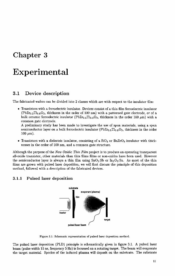
Figure 3.1: Schematic representation of pulsed laser deposition method.
The pulsed laser deposition (PLD) principle is schematically given in figure 3.1. A pulsed laser beam (pulse width 15 ns, frequency 3 Hz) is focussed on a rotating target. The beam will evaparate the target materiaL Species of the induced plasma will deposit on the substrate. The substrate
11

3. Experimental
is heated in order to obtain a high surface mobility. An oxygen partial pressure (0.2 mbar) is maintained in order to restare oxygen deficiencies. SrRu03 and PbZro.2Tio.s03 layers are grown at a deposition temperature of 600 oe c.q. 575 °C; as the semiconductor layers (Sn02:Sb or In20 3:Sn) are grown at a deposition temperature of approximately 500 °C. The advantage of PLD is that multiple layers directly and in-situ can be grown when the target materials are available. This is unlike other deposition methods, like MBE, where first effort has to be made to campose the right concentrations in the supply-containers. A disadvantage of PLD is the small deposition area, resulting in small wafers (smaller than one inch). Concluding, PLD is suitable for easy change of materials but not suitable for the production of devices.
3.1.2 Thin film ferroelectric field-effect transistor
A bottorn gate thin film device has been produced using all-oxide materials to obtain transparency. In order to grow an epitaxial gate and insuiator layer on the substrate, the gate layer is first deposited, whereafter insuiator and semiconductor layers are deposited. In IC technology it is common that the gate layer is deposited on top of the insuiator layer instead at the bottorn of the device. The semiconductor layer is a polycrystalline material as has been investigated by Grosse-Holzet al. [14]. The lithographic process to fabricate a device is as follows (a more detailed description is given in [15]):
• On a polished SrTi03 crystal (100) the gate material (SrRu03) is deposited. After a molybdenum layer is sputtered, a resist mask is spun. The desired pattern is defined with photolithography. The molybdenum layer is structured with reactive ion etching using a CF 4/02 plasma. The SrRu03 is etched away with a CHF3/ Ar plasma. The resist is removed with acetone whereafter the molybdenum leftovers are removed with an aqueous salution of K4Fe(CN)e/H202.
• After depositing (PLD) the PbZr0 .2Tio.s03 layer, semiconductive layer and its capping, a molybdenum mask is sputtered and patterned to define source, drain and the channel.
• In order to remave the semiconductor layer with its capping between the different devices at the wafer, the layers are etched away with CHF3/ Ar.
• To contact the gate, first aresist is spun, whereafter the PbZr0.2Tio.s03 layer is etched away with CHF3/ Ar.
• Finally, to separate souree and drain, a spun resist is patterned and molybdenum on top of the channel is removed with an aqueous salution of K4Fe(CN)6 jH202. The resist is removed with acetone.
This process results in a non-tatal transparent device as there are molybdenum contact pads. To obtain an all transparent device using highly doped In2 0 3:Sn as souree-drain contact material, two other process steps are used after making contactholes to the SrRu03 layer.
• After spinning resist, molybdenum on top of the contact pads is removed with an aqueous salution of K4Fe(CN)e/H202, whereafter an ln20 3:Sn layer is sputtered.
• After dry etching the ln203:Sn contact pads, molybdenum on top of the channel is removed to separate souree and drain.
Two kinds of masks ( called FET1 and FET2) are used, each containing several structures with different geometries, like metalfinsulatorjsemiconductor diodes, Hall bars, transistors and resistance test structures. In appendix B the layout of the two mask sets is given.
The layout and a cross-section of the device are depicted in figure 3.2 as well as a TEM picture and a photograph. In the photograph the text SOLID-STATE PHYSICS is placed under the wafer. Light shining through the wafer from the bottom, shows that the device is optically transparent. Table 3.1 gives a summary of the produced wafers with their characteristic parameters.
12

(a) The device layout.
{c) Photograph of the device, the text SOLID
STATE PHYSICS is placed under the wafer.
3.1. Device description
channel (JO nm Sn02:Sb) capping (JO nm BaZr03)
1250 nm
{b) Cross section of the device
(d) TEM picture of the device.
Figure 3.2: The thin film transparent field-effect transistor.
Transistor Wafer i gate tpzT tsc Sb doping tB zo nm nm nm cm-3 nm
Athin JC5376 140 250 10 4 1019 10 Bthin JC5404 35 350 25 8 1018 10 Cthin JC5375 110 250 10 4 1019 10 Dthin JC5383 50 225 5 4 1020 10 Ethin JC5386 20 250 12 4 1019 10 Fthin JC5401 35 350 10 4 1019 10 Gthin JC5463 35 350 15 4 1019 10 Hthin JC5385 20 250 7.5 4 1020 10
Table 3.1: Wafer number, thickness ofthe gate Jayer {tgate), the PbZro.2Tio.s03 insuiator (tpzT ), the semiconductor layer (tso), doping concentration, thickness of BaZrOa capping layer (tB zo) of all thin-film devices.
13

3. Experimental
3.1.3 Field-effect transistor with a bulk ferroelectric insuiator
Besides a thin film ferroelectric field-effect transistor, another field-effect transistor has been fabricated, containing a ceramic bulk ferroelectric insuiator (PbZro.sTio.s03), made with a sinter process (thickness is 0.18 mm). As a semiconductor, ln203:Sn has been used with two different doping-concentrations. After structuring the semiconductor layer with its capping, molybdenum contact pads are sputtered. The bottorn side of the bulk ceramic material contains a nickel-aHoy electrode. This sandwich is glued with a silver-powder suspension on a circuit board. The nickelaHoy electrode will function as the gate electrode (i.e., a common gate structure). In table 3.2 a summary of characteristic parameters is given.
Transistor Wafer tFE tsc Sn doping tB zo J.Lffi nm cm-3 nm
ABuLK JC5503 180 20 2 1020 10 BBULK JC5533 180 15 2 1018 25 CBULK JC5550 180 10 2 1018 25
Table 3.2: Wafer number, thickness of bulk ferroelectric insuiator (tFE), semiconductor thickness (tsc), doping concentration, thickness of BaZr03 capping layer (tBzo).
In the structuring processof wafers BB u LKand CBu LK an extra process step was inserted. Before sputtering molybdenum contact pads the wafers are dipped in HCl for 1 min. c.q. 3 min. in order to etch the BaZr03 layer. This has been done to investigate the possibility that the BaZr03 layer would form a contact resistance.
3.1.4 Field-effect transistor using spin-deposited materials
A Sn02 layer is spun upon a bulk ceramic PbZr0.5Ti0.5 0 3 layer, whereafter it is annealed at 500 °C for a few hours. The bottorn of the bulk ceramic material contains a nickel-alloy, which will function as the gate electrode. This sandwich is glued on a circuit board with a silver-powder solution. In table 3.3 characteristic parameters are given.
Transistor tpzr tsc Semiconductor doping nm cm-3
Aspun 180 J.Lffi 10 Sn02 -
Table 3.3: Ferroelectric insuiator thickness (tpzT), semiconductor thickness (tsc), semiconductor material, doping concentration. At the wafer, there is no capping layer present.
3.1.5 Thin film field-effect transistor with a Si02 insuiator
For the purpose of a possible gassensor, a Sn02:Sb layer without a BaZr03 capping layer is deposited on SijSi02 substrate (see table 3.4). Punching through the Si02 layer with a large voltage (>200 V) will contact the Si common gate. The thickness of the Si02 layer is 400 nm.
Transistor Wafer tsi02 tsc Sb doping tB zo nm nm cm-3 nm
As i JC5551 400 10 8 10111 -
Table 3.4: Wafer number, insuiator thickness (ts;o2 ), semiconductor thickness (tsc), doping concentration, thickness of BaZr03 capping layer (tB zO).
14

3.2. Measurement techniques
3.1.6 Thin film field-effect transistor with a BaZr03 insuiator
A Sn02:Sb layer without a BaZr03 capping layer is deposited on a BaZr03 layer which will function as the insulator. The SrRu03 layer is patterned and functions as the gate electrode. In table 3.5 a summary of the characteristic parameters is given.
Transistor Wafer tgate tazo tsc Sb doping nm nm nm cm-3
A a zo JC5184 88 300 100 8 10HS
Table 3.5: Wafer number, gate layer thickness (tgate), BaZr03 insuiator thickness (tBzo), semiconductor thickness (tsc ), doping concentration. No capping layer is present.
3.2 Measurement techniques
3.2.1 Measurement environment
The wafer to be characterized is placed in a closed compartment, which gives the possibility to insert a particular gas. Using micromanipulators with golden probes, contact can he made to the contact pads. To measure at higher temperatures than ambient, a hotplate (3 cm diameter) is used. This hotplate is mounted onto an adapted brick in which space has been made for supply wires as well as for a thermo-couple. The maximum temperature of this hotplate exceeds 1000 °C. For low temperature measurements a cryostat is used, where a helium flow cools the wafer down to temperatures of lOK. For the bulk ceramic wafers a voltage amplifier (gain factor = 100, max. 600 V) is used to apply a voltage to the gate electrode. The amplifier has been fabricated inside the laboratory.
3.2.2 Transfer charaderistic measurement
The relationship between In and Va is called the transfer characteristic. Using a HP Semiconductor Parameter Analyzer 4155A it is possible to set and measure current or voltage at the same time. In this case a voltage Va is applied to the gate electrode and a drain voltage to the drain electrode. The souree electrode is connected to the ground. In figure 3.3 the electrical circuit is depicted to measure the transfer characteristic.
G
Figure 3.3: Electrical circuit for the transfer charaderistic measurement.
15

3. Experimental
3.2.3 Polarization hysteresis measurement
Ferroelectric behaviour can be characterized with a Sawyer-Tower circuit (see figure 3.4) [16]. A reference capacitor Cref is placed in series with the ferroelectric capacitor. By applying an AC voltage (using a Philips PM5139 function generator) the displaced charge will cause a voltage drop over Cref. The applied voltage is monitored at the x-axis of a Tektronix TDS320 oscilloscope, while the reference voltage is monitored at the y-axis of the scope. To a good approximation, the polarization P is given by the amount of charge at the reference capacitor per unit area:
(3.1)
where Vref is the voltage drop over the reference capacitor and A the area of the ferroelectric capacitor. We have taken the polarization, P, equal to the displaced charge per unit area D using a differential form of Gauss's law: D = EoE + P, neglecting the term EoE. Taking typical values of a PbZro.zTio.sÜJ material for E (-106 V /m) and P (-0.2 C/m2 ), we get that EoE is much smaller than P (9 w-6 C/m2 ~ 0.2 C/m2
), causing equation 3.1 to be valid.
This measurement has been automatized with LABVIEW (see for a description appendix A.2). Note that insteadof a ferroelectric capacitor also a transistor can be used for this experiment. At the souree electrode the AC voltage is applied and the gate electrode is connected to the reference capacitor, while the drain electrode is ftoating.
x osc. y osc.
FE
Figure 3.4: Sawyer-Tower circuit
Three conditions have to be taken in account, fora correct measurement of the hysteresis:
• w ~ (RoscilloscoopCref )-1
: charge on the reference capacitor should not discharge over the oscilloscope,
• w ~ (RseriesCref )-1
: charge must be given a certain transfer time limited by a possible series resistance,
• Cref ~ Cterroelectric: the applied voltage must drop across the ferroelectric capacitor with a negligible drop across the reference capacitor.
3.2.4 Pulse measurement
Todetermine the switching speed of the deviceaso called pulse measurement has to be carried out. With the HP8161a pulse generator a positive voltage pulse with a pulse width and pulse height is applied to the gate. After a delay time of 5 seconds, the drain current is measured using the HP Semiconductor Analyzer HP4155A. Then a negative voltage pulse with the same height and pulse width is applied. The drain current is again measured. The ON-state and OFF-state currents are now determined at one specific voltage pulse. Varying the pulse width at a constant pulse height,
16

3.2. Measurement techniques
will give the minimum switching speed and varying the pulse height at a constant pulse width will give the minimum voltage needed to switch the transistor from one state to the other (see also appendix A.3).
3.2.5 Endurance measurement
Todetermine the endurance (i.e., the resistivity to repeated switching of the device), a squarewave is applied to the gate using a Philips PM6666 pulse generator. A programmabie counter counts the number of cycles (i.e., number of waves). At certain intervals the squarewave is switched off, and voltage pulses are applied to the gate to determine the souree-drain current in either two states. (For a explanation of the software see A.4.)
3.2.6 Relaxation measurement
To study the time evolution of the drain current, we have to perfarm a relaxation measurement. The drain current is sampled every 5.....,10 seconds with the HP4155A after a voltage pulse with a given pulse height and pulse width is applied to the gate. This can then be repeated for other voltage pulses varying the pulse height or pulse width. lt is also possible to set a bias voltage at the gate electrode (see for LABVIEW deseription A.5).
3.2. 7 Measurement of gate capacitance and transconductante
With the aid of equation 2.12, we can determine the mobility if we can determine the transconductance and the capacitance of the transistor. lt is useful to define the admittance, Y:
Y= ~ =G+jwC, (3.2)
where G is the measured conduetanee, w the radial frequency and C the measured capacitance. Using a HP Impedance Analyzer HP4192a, we can determine the admittance. The analyzer has four probes, and operates as follows. The analyzer sets an AC voltage, Vasc, with a bias voltage (Va) at output Heur and measures the current, I, fl.owing from Leur to ground. The voltage is measured over probes Hpot and Lpot· lt then calculates the admittance, and puts this output on a display.
s
G
e----{V V
Figure 3.5: Gate capacitance measurement (switch S open) or transconductance measurement (switch S closed) setup for the transistor. Hpot, Lpot, Beur and Leur are probes used by an impedance analyser, V and I are the measured voltage c.q. current.
In figure 3.5 a schematic representation is given ofthe four probes connected toa transistor. When we conneet Hcur to the gate, the gate-souree current will fl.uctuate is switchSis open, otherwise the souree-drain eurrent will fluctuate. We can measure this current by connecting Leur to the souree
17

3. Experimental
electrode. Connecting Hpot to the gate electrode and Lpot to the drain electrode, we measure the applied gate voltage. If the switch S is open, a two points measurement is performed which calculates the capacitance of the transistor. Care must be taken that the gate leakage current does not become not too high to disturb the capacitance measurement. Or in other words the frequency must be high enough to ensure that wC ~ G. When the switch is closed, a drain voltage, Vv, is set to the channel. The measured conductance G, is then equal to the transconductance 9m· Care must be taken that the frequency in wCa is not too high to disturb the measurement of the channel transconductance. Or in other words the frequency must be low enough to ensure that 9m ~ wC a. If the gate capacitance and transconductance are determined with a frequency sweep, the right frequency satisfying the two conditions, can then be chosen. Sweeping the gate bias voltage, the gate capacitance and transconductance are obtained as a function of the gate voltage, yielding a field-effect mobility according to equation 2.12. As well as the frequency sweep measurement as the gate voltage sweep measurement have been automatized using LABVIEW (see appendix A.6).
18

Chapter 4
Transistor characteristics
In this chapter we will first present transfer characteristics (i.e., Iv vs. Va) of the thin film transistor as wellas the ceramic transistor, followed by device speed measurements. The possibility of a contact resistance is then discussed and transfer characteristics, obtained using either a twopoints or four-points measurements, are compared. Finally the influence of the structuring process on the behaviour of the transistor is discussed.
4.1 Transfer characteristics
4.1.1 Thin film transistors
In figure 4.1(a) a hysteresis measurement is depicted measured at a transistor at wafer Cthin using a Sawyer-Tower circuit. From the figure the remnant polarization is about 0.2 C/m2 and the coercive voltage is about 2.5 V, nat unlike values found in literature [13][17].
0.3
0.2
0.1
~ 0.0
c.. -0.1
-0.2
-0.3
(a) Charge displace-ment. (Cref = 56 nF, A= 100x300 p.m2 , f =110Hz)
~ _o
10"6
10"7
10"8
10"9
10·10
10·11 -6 -4 -2 0 2 4 6
VG(V)
(b) Transfer characteristic.
(Vv = 0.1 V, L xW=5x300p.m2 ,
G=4p.m)
Figure 4.1: Displaced charge and transfer characteristic of wafer Cthin• measured at two different transistors.
In figure 4.1(b) the drain current vs. gate voltage is depicted. The hysteresis of the drain current has the same counter-clockwise circulation as the displaced charge. In the following transfer characteristics, the circulation direction is always counter-clockwise, unless noted otherwise. If we define the coercive voltage as the difference in gate voltage at the points with the steepest slopes in the transfer characteristic, the figure shows that this coercive voltage is also the same as the
19

4. Transistor characteristics
coercive voltage in panel (a). The increase of current in panel (b) below -3 V is due to gate leakage current, which is maximall nA at -5 V. In figure 4.2 besides the transfer characteristics the gate current is depicted. Panel (a) with a linear current scale is depicted to emphasize the transition between the ON- and OFF-state. Quite suddenly the current decreases as the gate voltage becomes larger than the coercive voltage. Panel (b) shows an ON/OFF-ratio of roughly two orders. It also shows some disturbance at -4 V probably due to initia! charging of the device. In Panel (c) the gate current is depicted. At -2 Vandat +2 V two peaks in the gate current occur and at +4 V an increase in current occurs. This increase is due to a leakage current through the insulator, but the two peaks are switching currents of the polarization. Charge has to move to get from one remnant state to the other remnant state and equals the remnant polarization plus the maximum displaced charge. The area of the current peak (~ x 3nA x 1 V) times the sweep speed (2.5 s/V) gives the total charge that is moved (4 ± 1 nC). The total charge per areal unit yields then 0.6 ± 0.2 Cjm2 which roughly equals the amount of charge needed to go from the remnant state to the saturated state ("""'0.5 C/m2 , see figure 4.l(a)).
10
i 5 _o
0
-4 -2 0 2 4
Va (V)
(a) Transfer characteristic depicted at a linear vertical scale.
2
< 0 .E.. _<!J
-2
~ -2 0 2 4
Va(V)
(c) Gate current. Note the difference between switching current and leakage current.
~ _o
10"6
10'7
1 o·6 L..-.L.,_~_._~_._~__,_~___.___, ~ 4 0 2 4
Va (V)
(b) Transfer characteristic depicted at a logarithmic vertical scale.
Figure 4.2: Transfer characteristics and gate current for wafer Athin· (Vv = O.lV, LxW=20x300J.im2, G=l6J.im)
When varying the transistor parameters like semiconductor layer thickness or doping concentration, we abserve different transfer characteristics. In figure 4.3, transfer characteristics are depicted
20

4.1. Transfer charaderistics
for several transistors. The figures shows that in panel (a) the transistor has got hysteresis but the ON/OFF-ratio is rather small due tothefact that the transistor contains too much charge for full depletion. For panels (b) to (f), the coercive voltage decreases as well as the maximum current. This can he explained as follows. The applied gate-voltage mainly drops over the semiconductor channel as the resistance is increasing. The ferroelectric layer experiences a smaller applied voltage causing a smaller coercive field. In other words, as the amount of charge carriers is decreasing from panel (b) to (f) the depolarization field is increasing, causing a smaller coercive field. As a result, the hysteresis loops become more slim.
~ _o
~ _o
10"5 / ;;;;; -10-6
10-7
10-8
10-9
10-10
10-11 -6 -3 0 3
Va(V)
(a) Ethin(LxW=20x300J.tm2 ,
G=16J.tm).
10"5
10-6
10"7
10"8
10-9
10-10
10"11 -6 -3 0 3
Va(V)
(d) Dthin(LxW=20x300J.tm2,
G=16J.tm).
6
6
-6
-6
-3 0 3
Va(V)
(b) Athin(Lx W=10x300J.tm2 ,
G=BJ.tm).
-3 0 3
Va(V)
(e) Gthin(LxW=12x50J.tm2 ,
G=BJ.tm).
6
6
':-~-"--~----''---~~~----' 10·11 ~ 0 3 6
-6
VG (V)
(c) Cthin(LxW=5x300J.tm 2 ,
G=4J.tm).
10-5
10-6
10-7
7 10-8
10"9
""""J 10-10
-3 0 3 6 10-11
Va (V)
(f) Fthin(LxW=10x250J.tm2,
G=6J.tm).
Figure 4.3: Different transfer charaderistics for several transistors. Note the figures have the same vertical as well as horizontal scales. (Vv = 0.1 V)
Camparing panels (a) to (c) we can conclude that it is hard to control the operation of the transistors as the semiconductor parameters are nearly the same (for details see table 3.1). The product eNvtsc is the samebut the figure shows that transistors in panels (b) and (c) are depleted and the transistor in panel (a) not. The difference in processing between the wafers is that the growth temperature of Bthinis 450 oe and of the two others 500 °C. Ref. (7] shows that with increasing deposition temperature the charge carrier density is decreasing
21

4. Transistor characteristics
due to chemical interaction of the PbZro.2Tio.s03 layer and the semiconductor layer, creating a dead layer and thus a smaller effective thickness. If we calculate the eN vtsc product taking values for Nv from Ref. [7], we get for panel (a) 1.0 ± 0.2 C/m2 and for panels (b) and (c) 0.32 ± 0.06 C/m2. This explains the non-full depletion of the transistor in panel (a). To illustrate the behaviour of the transistor while sweeping the ferroelectric at non-saturized loops or inner loops, several sweeps of displaced charge and transfer characteristic are depicted in figure 4.4, measured wat wafer Athin· For the inner loops it is quite remarkable that with only a small increase in displaced charge, the minimum current of the transistor is getting smaller by two orders of magnitude. Apparently the transition between depleting a part of the channel and the entire channel is small. This is the effect of the subthreshold slope. With only a little change in charge displacement, the conductance can change for over more than a few orders of magnitude.
0.10
0.05
'f 2. 0.00 a..
·0.05
·0.10
-4 ·2 0 2 4
V0 (V)
(a) Charge displacement measured at a MIS-diode. (! = 90 Hz, Cref = 56 nF, A = 200x200 pm2 )
1 o·•o '--.4...__...__.·2~__..o~---'-2~__._4-'
Vo (V)
(b) Transfer characteristic depicted at a logarithmic current scale. (Vv = 0.1 V, LxW=10x300pm2 ,
G=Bpm)
2x10-e
0
( c) Transfer charaderistic depicted at a linear current scale. (Vv = 0.1 V, LxW=10x300pm2 ,
G=Bpm)
Figure 4.4: Charge displacement and transfer characteristics of wafer Athin for several sweep voltages (equal line types correspond with the same sweep voltage amplitude).
22

4 .1. Transfer charaderistics
4.1.2 Transistors with a bulk ceramic PbZr0.5Ti0.50 3 insuiator
In figure 4.5 typical polarization curves for the ceramic bulk PbZr0.5Ti0.50 3 transistors are depicted, measured on wafer BnuLK· The outer curve is the saturated loop while the inners loops are measured with a smaller applied voltage sweep. The figure shows that the remnant polarization is 0.33 C/m2
. This value is similar to measured values on the other wafers.
0.4
0.2
~ 0.0
a. -0.2
-200 -100 0 100 200
V applied (V)
Figure 4.5: Polarization vs. applied fieldfora saturated loop and two inner loops. (Cref = 56 nF, A = 0.15 mm2 ,
f = llO Hz)
In figure 4.6 transfer characteristics of the three fabricated wafers with a bulk ferroelectric insuiator are depicted. In order to compare the three graphs we converted the drain current into sheetconductance, Go, to eliminate geometrie differences, using Go = Iv/Vv x LjW. Note that figure 4.6(a) has a linear current scale, while the current scales of the other two graphs are logarithmic. Panel (a) has a very small ON/OFF-ratio ("'1.1) and for panels (b) and (c) this ratio increases (3.3 to 19). The conductance of the ON-state is roughly the same in panels (b) and (c) if we consider the thickness differences [(b) 15nm and (c) 10 nm].
If we calculate the charge per unit area in the semiconductor layer using Q =eN vtsc, we obtain for the three wafers: 51 ± 5, 0.48 ± 0.05 and 0.32 ± 0.03 C /m2 . The polarization modulates the charge in the semiconductor channel with an amount of 0.4 Cfm2 (see the inner loop in figure 4.5), so we can see that is impossible to deplete waferA nu LK as it contains too much charge. We also see that as the charge in the semiconductor layer decreases, the channel-depletion increases (panels (b) and (c)). In the figure the coercive voltage is about between 55 and 70 V, while in the displaced charge curve (figure 4.5) the coercive voltage amounts 120 V. We attribute this difference to the relaxation of the ferroelectric. The transfer characteristic is measured a low frequency ( "'0.03 Hz), while the sweep frequency of the displaced charge measurement is 110 Hz. The relative differences in coercive voltages between panels (a), (b) and (c) could he explained by the differences in conductance. The wafer in panel (c) has a lower conductance than the wafer in panel(a). When a gate voltage is applied, there could he a electrostatic potential drop present across the channel. This drop would result in a less effective potential across the insuiator and thus the coercive field would increase.
23

4. Transistor charaderistics
0.64
éii 0.62 E
~ 0.60
0.58
CJ
-100 100
(b) BBULK (LxW=lOx250pm2 )
-100 100
Figure 4.6: Transfer charaderistics for three transistors with a bulk ferroelectric insulator. Note the different scales on the vertical axes.
4.1.3 Thin film field-effect transistor with a Si02 insuiator
In figure 4.7 the transfer characteristic is given for wafer Asi· Note the large applied gate voltage of 100 V. The figure shows that there is a field-effect which is linear as we are used to hysteresis behaviour, but with small a ratio of about 2 between the maximum and minimum drain current. The leakage current (not shown) is smaller than 0.1 nA at 100 V. If we calculate the displaced charge at the insulator/semiconductor interface, we obtain (using Q = CV = EoErV/d) Q= 6 mC/m2 (Er= 2.6, V= 100 V, and d = 400 nm). The amount of charge carriers in the semiconductor layer, eNvtsc, yields 1.3 C/m2
• Thus it is quite obvious that the insuiator and the semiconductor layer are too thick for full depletion of the channel. From the slope of the transfer characteristic and the above calculated displaced charge, we can calculate the field-effect mobility using equation 2.7, which yields 20 cm2 /Vs.
24

4.2. Transistor with a spun Sn02 semiconductor and a bulk ferroelectric insuiator
35
~ 30
l _o
25
20
-100 -50 0 50 100
VG(V)
Figure 4.7: Transfer characteristic of As;. (Vv = 0.1 V, LxW=25x200JLm2 )
4.2 Transistor with a spun Sn02 semiconductor and a bulk ferroelectric insuiator
In figure 4.8 the transfer characteristic of wafer Aspun is depicted. The figure shows proper hysteresis behaviour with an ON/OFF-ratio of 500, but there is a difference of five orders in the minimum and maximum conductance. Note that the minimum current is not limited by the influence of a gate leakage current, in contrast to the transfer characteristics of the thin film ferroelectric transistors. The charge displacement is not depicted as the semiconductor layer at the wafer is not structured, causing a too large electrode area for the hysteresis measurement.
-100 0
VG (V)
100
Figure 4.8: Transfer characteristic of wafer Aspun (Vv = 10 V, LxW=10x300JLm2 ).
4.3 Device speed
The device switch speed can be determined with a pulse measurement. That is, a voltagepulseis applied to the gate electrode and after a delay time of five seconds, the drain current is measured. This action is repeated for a variabie pulse height while the pulse width is kept constant or for a variabie pulse width while the pulse height is kept constant. So the channel conductance is successively switched to the ON-state or to the OFF-state. In figure 4.9(a) the measurement is performed varying the pulse width with a constant pulse height (5V). In figure 4.9(b) the pulse height is varied at a constant pulse width (1 ms). In figure 4.9(a) both ON-state and OFF-state current are depicted as a function of the pulse height. At high applied voltages the ON-state current is constant, and decreases when the pulse height is
25

4. Transistor charaderistics
••• ......... . ..
•• -····· •• .. ·~
• • lncrease due to . charge injection . \ •..•... ···
pulse height (V)
(a) Variation of pulse height at a constant pulse width (lms).
o·s .. 1 !la·••;::- ·-....- •••••••
.. . .. . \ . \, .•.
·, .• ........ •
• \ \..-•······ \, t
10'7 1..1...,~~ ....... ~~ ....... 7""~ ...... ~ 10'7 10'6 10'5 10'4 10'3 10'2 10'1
pulse width (s)
(b) Variation of pulse width at a constant pulse height (5V). The arrow indicates the theoretica! value for the switching time. The dashed line represents the function: lv "'r-1.
Figure 4.9: Pulse measurement at wafer Athin· (LxW=20x300 JLm 2, G=l6J.tm).
getting below 3 V. For the OFF-state current the figure shows a decrease in current from a pulse height from 5 V to 3.5 V and then an increase when the pulse height is getting smaller. In figure 4.9(b) the ON-state and OFF-state current are depicted as a function of the pulse width. The OFF-state current is constant above large pulse widths but the current increases when it gets below 0.3 ms. The ON-state current remains nearly constant except for a small decrease when the pulse-width gets below 1 t.ts.
The switching of the transistor with variabie pulse height can be divided in three parts. At pulse heights below 1 V the ferroelectric layer is not switched by the applied voltage pulses. Between 1 V and 3.5 V the ferroelectric layer switches in non-saturized states and becomes saturized at 3.5 V. At larger applied voltages charge injection (see theory section 2. 7) occurs, which causes the OFF-state current to increase. Charge injection is not observed in the ON-state current. Panel (b) shows that there is a minimum switching time of roughly 0.3 ms. Using equation 2.16, a theoretica! value is given for the switching time and yields 0.3 ms. This value is illustrated with the arrowin panel (b). In table 4.10(a) the experimentally obtained minimum switching times vs. theoretica! values are given and depicted in figure 4.10(b). The figure shows that the experimental data corresponds with the theoretica! values. The drawn line is the line when theory and experiment coincide. In panel (b), below the minimum switching time of 0.3 ms the OFF-state current increase. The slope of this part of curve is roughly parallel to the plotted dashed line, which represents the function: In "'r-1 as predicted in the theory section 2.9. The ON-state currents in both figures are fiat. We attribute this to the presence of series-resistances limiting the channel conductance. Placing resistors in series with the channel, we observed a decrease in the ON-state-current equal to the conductance of the resistor (not shown). The ON-state current behaviour still remains fiat. In the case that the channel resistance is larger than any series resistance we will observe even in the ON-state current charge injection as will be shown in chapter 5 (Endurance experiments).
For the ceramic transistor, the device switching speed measurement shows that the transistor could switch down to switching times of 1 ms. Due to the band-width of the voltage amplifier we could
26

Wafer Ttheor Texper
ms ms Cthin 15 25 Athin 0.3 0.3 Dthin 15 10 Ethin 0.12 0.3 Bthin 0.6 2
(a)
10
.. (ij
~ 1 E
"55 c. >< Q)
0.1
•
0.1
4.4. Contact resistance
• •
•
10
theoretica! t (ms)
(b)
Figure 4.10: Table and figure of theoretica! and experimental minimum switching times obtained at different wafers.
not measure below 1 ms. Theoretically this minimum pulse width time would he in order of 1 J.LS in case of transistor CBULK·
4.4 Contact resistance
The total resistance of the channel, Rror, depends on the geometry of channel (i.e., length and width) and depends on a possible contact resistance, Rcontact:
L RroT = W Ro + Rcontact ( 4.1)
We can determine Rcontact by measuring the channel resistance for several souree-drain lengtbs and widths at a single wafer. In figure 4.1l(a) the resistance vs. souree-drain length is depicted. The resistance is obtained in the absence of a gate voltage after a positive gate voltage is applied of +4 V. A contact resistance for wafer Athin is determined to 10 kn by extrapolating the trend taking L to 0. For other wafers the contact resistance is in the range of 10"'50 kn. The resistance for several channel widths is depicted in figure 4.11(b). Extrapolating the trend taking W to infinity, the figure shows that there is no axis offset. This has also been observed for other wafers.
From these two measurements we can conclude that there is a contact resistance in the order of 10 kn, and that the contact resistance is a phenomenon that is uniformly spread over the entire contact pad. The BaZr03 layer between the contact pad and the semiconductor channel is probably obstructing the conductance. Therefore in wafer BBULK the BaZr03 layer is removed by etching for 1 minute in HCl, after which the molybdenum contact pads are sputtered. In figure 4.11(c) the resistance of this wafer is plotted with channellength variation. The figure shows that the curve has a smaller axis offset of about 1 kn. At wafer CBULK the BaZr03 layer was etched for 3 minutes in HCl, resulting in a contact resistance of 2 kn. At several intervals in the etching process the conductance is measured by placing two probes at one contact pad. The resistance measured by placing two probes at the semiconductor layer, increased during the etching process from 40 kn to 2 Mn. Etching with HCl can he convenient to reduce the contact resistance, however care should he taken that the etching Huid does not affect the semiconductor layer.
27

4. Transistor characteristics
30 30 10
• • 8 .. ..
20. 20 6 • Ir
ê ê ê ~ ~ ~
Ir a: a: a: 4 IJ{
10 ~ 10
:i Ji
2 • .. Ir .. 0 0 0 100 200 0.00
0 0.05 0 100 200 300
L (lun) w·,(llm.,) L(11m)
(a) Channellength variation (b) Channel width variation ( c) Channel length variation
for Athin(W=300 JLm). for Athin(L=lOO JLm). for BBULK(W=250 JLm).
Figure 4.11: Resistance as a function of either souree-drain length or width.
4.5 Two-points and four-points measurements
The transfer characteristic can he measured witheither a two-points or a four-points measurement. The advantage of a four-points measurement is that a possible contact resistance or supply-wire resistances are elimated. We will campare three four-points measurements, which will he first described whereafter a comparison with the two-points measurement will follow. In figure 4.12(a) a top view of the transistor channel is given, which are present on the mask set FET1 (see appendix B). There are four contact pads on top of the channel, between contact pads two and three the gate is positioned. In a two-points measurement a voltage is set over contact pads two and three, while the current through contact pads two and three is measured. In a four-points measurement a current is driven through contact pads one and four, while the voltage is measured over contact pads two and three. Instead of measuring the voltage over contact pads two and three, the probes can alo directly be placed on top of the channel. In an ideal voltagemeasurement device no current is fl.owing through the probes so no voltage drop will occur at the BaZr03 capping-layer. The third four-points measurement is to use a gated Hall-bar, i.e., a Hall-bar structure with underlying gate which are present on mask set FET2 (see appendix B). A top view of a gate Hall-bar is depicted in figure 4.12(b). In figure 4.13(a) the two-points and four-points measurement are depicted measured at a transistor with the layout as shown in figure 4.12(a) at wafer Athin· The conductanceis obtained in the twopoints measurement by applying a drain voltage of 0.1 V and measuring the current, and in the four-point measurement by setting a channel current of 10 nA and measuring the voltage. The curves show good resemblance. At first sight this would mean that there is no contact resistance present. At second sight, takinga closer look at the layout of the device (Fig. 4.12(a)), we see that when measuring the voltage drop across the channel, the voltage is not measured at one point but over an area. So an average voltage is measured which results in an extra resistance. If we assume that this extra resistance is of the same order as the contact resistance, it is logica! that the two curves coincide. If the two inner contact pads were thin, the problem would not have arisen. We can bypass this problem by placing the two voltage probes directly on the BaZr03 capping-layer on the channel between contact pads two and three. In figure 4.13(b) the channel conductance is given. Note that there is still a gap in the curve at Va = -2 V for the same reason as mentioned above. The conductance in the ON-state is about 0.1 mS. When we campare this conductance with the conductance in the two-points measurement, we should take in mind that the two probes are closer positioned causing a higher conductance.
28

gate
conta~ _ ~ __
~ +
channel
(a) Top view of the transistor; contact pads and underlying gate are also plotted.
4.5. Two-points and four-points measurements
(b) Top view of a gated Hall-bar: contact pads and underlying gate are also plotted.
Figure 4.12: Two different layouts of a transistor to perferm a four-points measurement.
10-4
10-5 .. Ui' ;-1o·6
10-7
10-8 -4
-a- Two points messuremen ___._ Four points maasuremen
-2 0 2 4
VG(V)
(a) Two- and four-points measurement.
/':"/
/
(b) Four-points measurement with probes positioned on the top of the channeL
Figure 4.13: Two- and four-points measurement at wafer Athin· In the four-points measurement at Va = -2 V there is a gap noticeable. In this region the switching current of the ferroelectric layer is disturbing the voltage measurement, causing the driven current to flow from drain to gate and not to source, which results in noise. (LxW=100x300 f.Lm2 , G=100 f.Lm).
29

4. Transistor charaderistics
To estimate the contact resistance, we have to take in account for this geometrie increase in conductance. The geometrie factor is obtained by camparing the OFF-state conductances in both figures, as the contact resistance is then negligible. The geometrie factor yields roughly 6. Multiplying this factor with ON-state conductance in figure 4.13(a), we can campare the two conductances in both figures and the difference will give the contact resistance ("' 20 kf2). This contact resistance is in good agreement with the contact resistance determined in the previous section.
---0-- Two points maasurement --- Four points maasurement
-4 -2 0 2 4
Va(V)
(a)
Figure 4.14: Two- and four-points measurement at a gated Hall-bar. (wafer Bthin)
Using a gated Hall-bar structure, the transfer characteristic of a transistor at wafer Bthin has been derived. In figure 4.14 the two- and four-points measurement are depicted using gated Hall-bar 3 (see figure 4.12(b) fora top view of the gated Hall-bar). Inthetwo-points measurement a drain voltage of 0.1 V is applied at contact pads two and three while the current is measured. In the four-points measurement a current of 100 nA is driven through contact pads one and four while the voltage drop is measured over contact pads two and three. The figure shows that in the two-points measurement the ON-state resistance is about 0.3 ~tS and in the four-points measurement about 10 fLS. The contact resistance is not the difference between the reciprocal of these two numbers, as in the two-points measurement there are series resistances due to the presence of the contactpaths and the current-path in the two-points measurement is larger by a factor of roughly three. The contact resistance will then be about 1 Mn which is quite large in comparison with the contact resistance obtained from the channellength variation. The ON/OFF-ratio is in the two-points measurement is about 2 and about 10 in the four-points measurement. Soit seems likethereis a contact resistance present.
4.6 Increase in channel conductance due to structuring
Directly after the deposition of the semiconductor layer with its capping layer, the conductance of the semiconductor layer is measured by placing two probes with indium cantacts on top of the semiconductor layer near the edge of the wafer. In all fabricated wafers this conductance is lower than the conductance after structuring (i.e., the entire process between depositing the semiconductor layer and defining the semiconductor channel). For the wafers with an Sn02:Sb semiconductor film the conductance per square ( denoted by ~G) increases by an amount in the order of 10-5 S while for the In203:Sn semiconductor wafers the increase is in the order of 10-4 S. In order to investigate this phenomenon, several wafers are made with various semiconductor layer thicknesses. After deposition of an In20 3:Sn semiconductor layer (Nv = 2 1018 cm-3) a molyb-
30

4.6. Increa.se in channel conductance due to structuring
denurn film is sputter-deposited and removed with an aqueous salution of K4Fe(CN)6 JH2 0 2 . In table 4.1 the measured conductivity as well as the increase of conductance befare and after the molybdenum remaval is summed up for the various thicknesses.
Wafer tsc tB zo CTbefore CT af ter !:l.G (nm) (nm) (nm)-1 (nm)-1 (1o-4S)
JC5529 150 10 7.0 10:.! 3.7 10J 4.5 JC5530 15 10 6.0 102 2.0 104 2.9 JC5533 15 25 1.3 102 7.5 103 1.1 JC5534 5 25 8.0 101 4.2 103 0.2
Table 4.1: Wafer number, semiconductor layer thickness (tsc ), thickness of BaZr03 capping layer (tB zo, conductivity before and after molybdenum removal (ubefore and Uafter) and the increa.se in conductance (LlG).
The table shows that the increase in conductivity is roughly the same for a 15 nm or 150 nm semiconductor layer. Only for a 5 nm layer the increase is one order of magnitude smaller. These values show that the semiconductor layer is affected by the remaval process and an affected layer which is created, is larger than 5 nm. To calculate the affected layer thickness, we assume that the semiconductor layer of the 5 nm sample is totally affected and that the wafers with the 15 nm or 150 nm semiconductor layers are partially affected over a thickness ó (see figure 4.15). The partially affected semiconductor layer consists now of two parallel resistances, one with high conductivity ( the affected part) and one with a low conductivity (the non-affected part). We take for the conductivity of the affected part the conductivity of the 5 nm wafer after molybdenum remaval and we take for the conductivity of the non-affected part the conductivity of the wafer befare the molybdenum removal. The total conductance of the semiconductor layer after structuring ( thickness times conductivity) yields then:
tsc CTafter = (d- ó) CTbefore + Ó CT5nm,aften (4.2)
where tsc is the thickness of the semiconductor layer. This equation results in an affected layer of 13 nm for the 15 nm wafers and 17 nm for the 150 nm waf er.
capping layer
semiconductor layer
totally affected
t -s se
partially affected
capping layer
semiconductor layer
affected
non affected
Figure 4.15: Schematic representation of a totally affected semiconductor layer and a partially affected semiconductor layer over a thickness /i. The semiconductor layer remains non-affected over a thickness of tsc -/i.
We verified that K4Fe(CN)6 /H20 2 (the fluid to etch molybdenum) is not the cause of the increase increase. A wafer with an Sn02 :Sb semiconductor layer with a 10 nm BaZr03 layer on top has been put in the etch fluid for several minutes ("'15 minutes). The resistance remains the same during the experiment. Dry etching (with a Barrel etcher) in stead of wet etching still gives an increase of conductance. We might conclude that the semiconductor layer is affected by the molybdenum sputter process. 1t is possible that the semiconductor layer is modified but it is hard to confirm this as camparing the semiconductor structure befare and after molybdenum remaval is difficult. SIMS spectroscopy shows that there is indeed a large molybdenum concentration in the BaZr03 layer. Due to this large concentration, it is not possible to measure whether there is molybdenum inside the semiconductor
31

4. Transistor characteristics
layer. With this measurement, it was not possible to obtain absolute values of molybdenum concentrations, only relative values compared to a reference sample could be given. For future studies, it is worthwhile investigating molybdenum evaporation instead of sputtering, as the energy of molybdenum ions in an evaporation process is much lower. Another possibility to eliminate the molybdenum influence, is to use other materials for masking like, for example, lacquer.
32

Chapter 5
End urance experiments
Knowledge about the life-time of a device is important, especially when the device is implemented in an application. In this chapter we will investigate the endurance or the fatigue behaviour of the devices. The concept of endurance is the insensitivity of the device to repeated switching, while the concept of fatigue is that irreversible changes in the device originate from repeated switching. So after the device has become sensitive to repeated switching, the fatigue of the device has started. We will compare the endurance of ferroelectric devices with a bulk or a thin film ferroelectric insulator, and the endurance of devices containing a dielectric insulator. In the fatigue experiment we will apply a square wave voltage at the gate electrode at the highest frequency as possible, in order to reduce the total measurement time. At several intervals, transfer characteristics are determined and the ON-state and OFF-state currents are obtained by switching the channel in either state using a voltage pulse.
5.1 Thin film transistors with a ferroelectric insuiator
In figure 5.1 results of an endurance experiment performed at a transistor of wafer Athin, are depicted. At a frequency of 100 Hz a square wave is applied to the gate with amplitude of 4 V. During the endurance experiment several transistor characteristics are measured, like transfer characteristics, ON- and OFF-state currents and pulse measurements. The ON- and OFF-state currents are determined by applying a voltage pulse of 4 V and a pulse width of 5 ms. Transfer characteristics measured before, during and after the fatigue are depicted in figure 5.1(a). Before the start of the endurance measurement, the transfer characteristic is quite rectangular but as the number of passed cycles increases (from 104 up to 107 cycles), the curve is getting more slim. The coercive voltage decreases as wellas the maximum current. The gate current at +4 V (not shown) increases from 0.5 nA at the start of the experiment, up to 9 nA after 107 cycles. The ON- and OFF-state currents at several intervals are depicted in figure 5.1(b). The figure shows that the ON-state current immediately decreases as the OFF-state current increases up to 105 cycles whereafter it tends to decrease. The ON/OFF-ratio depicted in figure 5.1(c) shows a decrease almost linear with the logarithm of passed cycles.
Pulse measurements measured before the fatigue and after 107 cycles are depicted in figure 5.2. Panel (a) shows clearly a difference between the measurement before the fatigue and at the end of the fatigue (107 cycles). Before the fatigue, the voltage necessary to switch the channel conductance toa minimum or maximum value, is about 2.7 V and after the fatigue about 3.5 V. Before the endurance experiment the ON-state current shows no charge-injection, whereas for the OFF-state current charge injection occurs. After the fatigue the pulse measurement is different. The ON-state current is decreased and there is even charge injection noticeable. The OFF-state currents in both cases coincide at voltages smaller than 1.5 V or larger than 3.5 V. Panel (b) shows the pulse measurement with a variabie pulse width (pulse height = 5 V). Again the ON-state current is smaller than the current before the start of the endurance measurement.
33

5. Endurance experiments
~ _o 10-s
--before fatigue
- • • aftar 9 104 cycles
- - after 3 107 cycles
-4 4
(a) Transfer charaderistic at three different numbers of passed cycles.
103 104 105 106 107
N (cycles)
(b) ON- and OFF-current evolution.
u. u. 0 -i=-
100
q_ 10
-... .... .. ... . . · ... ~ ... .. ..._ • .... . · ..... . ......
1~~~~~~--~~~~ 1~ 1~ 1~ 1~ 1~
N (cycles)
(c) ON/OFF ratio.
Figure 5.1: Endurance measurement at wafer Athin (!=100Hz, pulse height 4 V, Vv = 0.1 V, LxW=10x300JLm2 ).
34

5.2. Transistors with a bulk ferroelectric insuiator
.................. · · · • · · before fatigue
... after 3 107 cycles
0 2 3 4 5
pulse height (V)
(a) Variation of pulse height at a constant pulse width (999 ms).
6
······:·::: .... •·•···•·· ..... ······· .... .. .. .. · · · ·• · · · befare fatigue
·· ...... aftar 3107 cycles
10"7 10-6 10"5 10"4 10-3 10-2 10"1 10°
pulse width (s)
(b) Variation of pulse width at a constant pulse height (5 V)
Figure 5.2: Pulse measurement measured during the same endurance experiment as in tigure 5.1.
The minimum pulse width increases from 2 ms to 40 ms.
The transfer characteristics show that the coercive voltage decreases. This could indicate that there is a dielectric layer created at the semiconductorfinsulator interface. Pulse measurements show that the voltage necessary to switch the device properly, is increased due to repeated switching. When a voltage pulse is applied, there is a voltage drop across this possible dielectric layer causing the effective voltage drop across the ferroelectric layer to he smaller. The switching time of the transistor is also increased during the endurance measurement. We can attribute this increase to the creation of a possible dielectric layer. Panel (a) and (b) show that the minimum current or the maximum resistance remains roughly the same. As the switching time is related to an RC time, it means that a capacitor C and thus a dielectric layer, has been created during the endurance measurement. These three statements give enough evidence to sustain the idea that the semiconductor channel is affected, resulting in a dielectric layer.
5.2 Transistors with a bulk ferroelectric insuiator
5.2.1 Charge displacement
Results from endurance experiments with a bulk ferroelectric capacitor are depicted in figure 5.3. Figure 5.3{a) shows three displaced charge measurements, measured before the start of the endurance measurement, after 4 105 and 4 106 cycles. The remnant polarization decreases with a factor of 1.4 after 4 106 cycles. Note that the coercive voltage remains the same. Two remarks should he made while observing the wafer during the experiment. The piezoelectric effect of the ferroelectric insuiator was visible through a microscope, because the refiection of the light shining at the surface of the wafer was oscillating at the spot of the transistor. Secondly, the exterior of the molybdenum contact pads changed. Through a light microscope, it was noticeable that the sticking of the molybdenum was not good and that the surface had become fiaked off. The semiconductor did not conduct below the contact pads at the places where the molybdenum had come off (R > GO). Using a smaller sweep amplitude {150 V, f = 1 kHz) we observed a decrease of 10% in displaced charge after 2 106 cycles, the displaced charge then remained constant up to 7 106 cycles (not shown).
35

5. Endurance experiments
In figure 5.3(b) we scaled the curve of the charge displacement after the fatigue with a factor of 1.4. This up scaled curve roughly coincides with the curve measured before the fatigue. This proves that the reduction in charge displacement after the fatigue is due to a surface reduction. In case of the creation of a dielectric layer at the semiconductor/ferroelectric interface, we would expect a lower remnant polarization, but the coercive field would decrease as the ferroelectric is sweeping at inner loops. However we cannot exclude the possibility of the creation of a dielectric layer. As the ferroelectric insuiator has a large impedance due to the large thickness, compared to the semiconductor thickness (180 J.tm vs. 10 nm), the possible dielectric layer can not infl.uence the charge displacement.
Thus, although it seems that the ferroelectric capacitor shows fatigue, we can conclude that it is a contact electrode effect. The piezoelectric effect of the insuiator causes the molybdenum to fl.ake off, yielding a smaller contact area. At smaller applied voltages this is effect is smaller. For the thin film ferroelectric layer no fatigue was observed after 106 switching cycles.
0.4
0.2
~ 0.0
Q. c.. -0.2
-0.4
·200
-before fatigue • • • after 4 105 cycles
- - after 4 1 o• cycles
200
(a) Displaced charge measured at several intervals during the fatigue measurement (see inset).
0.4
0.2
~ 0.0
Q. c.. -0.2
·0.4
-200
-before fatigue - - after 4 106 cycles -idem but scaled
with a factor 1.4
200
(b) Displaced charge measured before and after the fatigue. The thin line represents the measurement after the fatigue but scaled with a factor of 1.43.
Figure 5.3: Displaced charge at transistor BBULK (f = 1 kHz, Cref = 56 nF, A= 0.18 mm2 ).
5.2.2 Thansfer characteristic
In figure 5.4(a) ON- and OFF-state currents are depicted, measured during an endurance experiment. The figure shows that the ON-state current to he rather constant up to 104 cycles whereafter it decreases. The OFF-state current decreases almost quite linearly with the logarithm of time. At other samples the ON- and OFF-state current often collapse to a highly resistive state (R > Gn), after 106
"' 107 cycles (not shown). Figure 5.4(b) shows first an increase in ON/OFF-ratio and after 105 cycles the ratio drops from 10 to 3. We showed in the previous section (5.2.1), that the ferroelectric does not show any fatigue behaviour. Therefore the decrease in ON- and OFF-state currents must he due to fatigue of the semiconductor channel. This can occur in two possible ways, namely by the creation of cracks in the semiconductor caused by the piezoelectric effect of the insuiator or by the creation of a dielectric layer at the semiconductor/ferroelectric interface at the cost of the semiconductor layer. Due to the displaced charge, each cycle a switching current will flow, causing the semiconductor to degrade locally.
36

5.3. Wafers with a dielectric insuiator
10"6 .......,~"""-:,._.............,~"""-:~"""-:~.......", 102 103 104 105 106 107
N (Cycles)
(a) ON- and OFF-state versus the number of switched cycles.
u. u. CL z-CL
10
~·· .. ~ . . ~ ..
• . . • . ·.
1~~~~~~"""--:,........"""-:~~ 1~ 1~ 1~ 1~ 1~ 1~
N (Cycles)
(b) ON/OFF-ratio versus the number of switched cycles.
Figure 5.4: Endurance measurement at transistor CBULK (!= 100 Hz, pulse height 120 V, Vv LxW=25x200 pm2).
5.3 Wafers with a dielectric insuiator
5.3.1 Thin film field-effect transistor with a BaZr03 insuiator
0.1 V,
As an interesting comparison, we investigated the influence of the ferroelectric insuiator on fatigue behaviour, we used sample ABzo, as it has a dielectric insulator. At a frequency of 100 Hz, a square wave with amplitude of 3 V is applied to the gate electrode. In figure 5.5(a) the ON- and OFF-state currents are depicted as a function of the number of switching cycles. The figure shows that bath curves progress the same way. The currents first decrease and start to increase after 4 105
pulses. The difference in currents of the two states (i.e., J 0 N - JOFF) is roughly the same during the fatigue test. In other words, the modulation of the channel conductance (i.e., the field-effect) is the same. In figure 5.5(b) the ON/OFF-ratio is depicted. The figure shows that the ratio starts at a factor of 1.3 to 1.5 and then decreases. This can be attributed to the increase in the ON-state and OFF-state currents.
_o
3.0
2.5 . · • • • .. . ... .. .. .................
... .. .
• •
. •
.··•· • 2.0 ..
• .. ...... . .. 1.5 ...................... •
1if 104 10S 106 107
N (cycles)
(a) ON- and OFF-state versus the number of switched cycles.
u. u.
1.50
......
.. ........... . .... •. ... •. .,. . .. "" ·~ ..... .. ~ 1.25 CL
1.00 ......._,......_".............__~"""-:~""'--:'6~""--::'-7 ........... 103 104 105 10 10
N (cycles)
(b) ON/OFF-ratio versus the number of switched cycles.
Figure 5.5: Endurance of sample ABzo (f = 100Hz, pulse height = 3 V, Vv =0.1 V, LxW=100x300pm2).
37

5. Endurance experiments
The increase in currents can be attributed to external influences, as there is no BaZr03 capping layer present on the semiconductor layer and the measurement time is roughly one day. The main condusion to be drawn from this experiment, is that the transistor does not show any fatigue up to 107 cycles.
5.3.2 Thin film field-effect transistor with a Si02 insuiator
With sample Asi a fatigue experiment is performed using a square wave with amplitude of 9 V and a frequency of 1 kHz or 100 kHz. After 6 107 the frequency was raised to 100 kHz. We experimentally verified that the transistor can operate at frequencies of 100 kHz. Figure 5.6(a) shows an increase in current of about 5%. Another experiment shows a decreasein current of the same order (not shown). From the figure it follows that the difference in current of the two states is rather constant ( ...... 2 J.LA). The ON/OFF-ratio is also constant during the fatigue. We attribute the changes in current to external influences as the experiment lasts fora long period of time (.....,1 day). We can conclude from this experiment, that the device does not show any fatigue.
36
104 105 106 107 108
N (Cycles)
(a) ON- and OFF-state versus the number of switching cycles.
u. u.. 0 ~ Q..
. .... 1.05
1.00 ............. ..,.... ....... ="""'".......,,......-=7,......""'":' ......... 104 105 106 10 108
N (Cycles)
(b) ON/OFF-ratio versus the number of switching cycles.
Figure 5.6: Endurance measurement of a thin film silicon field-effect transistor(!= 1 kHz ( < 6 107 cycles), f = 100 kHz(> 6 107 cycles), pulse height = 9 V, Vv = 0.1 V, LxW=25x300J.Lm2 ).
5.4 Summary and discussion
The experiments with the ferroelectric transistors have shown fatigue behaviour which becomes crucial after 107 cycles. At that point, the ON-state current have become equal to the OFF-state current within one order of magnitude for the thin-film field-effect transistors. For the field-effect transistor with a bulk ferroelectric insulator, the ON-state current after 107 cycles becomes equal to OFF-state befare the start of the fatigue measurement. The endurance of the thin-film transistor is better, because during the switching cycles the OFF-state current is rather constant causing a clear difference between the ON- and OFF-state current, in contrast to the bulk ferroelectric transistor where the ON-state current becomes equal the OFF-state current. We have excluded the possibility of ferroelectric fatigue. Other research shows that ferroelectric fatigue shows up after 109 ...... 1010 cycles (18][19]. The semiconductor layer can be affected due to three reasons. The piezoelectric effect of the insuiator can cause cracks in the semiconductor layer. The transistors with a dielectric layer showed no fatigue, this could mean that the amount of charge that is switched during each cycle, creates defects at the cost ofthe semiconductor layer. Chemical
38

5.4. Summary and discussion
interaction at the semiconductor finsuiator interface could cause degradation of the semiconductor layer. For example, when charge carriers with a high energy are filling defect states, the energy is liberated and can cause more defect states.
39

5. Endurance experiments
40

Chapter 6
Light dependenee and temperature behaviour
In this chapter we will discuss the influence of light on the transistor behaviour. Then the temperature behaviour in a range of 20 K to 600 K will be discussed of the thin film as well as the bulk ferroelectric field-effect transistor.
6.1 Light dependenee
10"6
10"7
~ 10"8 _o _o
········· dark 10"9
- - - ambient light - miserescope light
10-13 ........ _._ .......... ___._~_,_~_,_~_._....._" 10-10
- - - ambient light - miscroscape light
-2 -1 0 2 -4 -2 0 2 4
VG(V) VG(V)
{a} Fthin {LxW=10x250 pm2 ). (b} Dthin (LxW=20x300 pm2 }.
Figure 6.1: Transfer characteristics of wafer Fthin and Dthin under different light conditions (Vv = 0.1 V).
In figure 6.1 transfer characteristics of two wafers are depicted measured at different light conditions. Figure 6.1(a) shows three different transfer characteristics of wafer Fthin, measured in dark, in ambient light and with light added from with a microscope lamp. The curve when the wafer is placed in dark, is very slim and broadens when the wafer is placed in normal room light or when light from a microscope is added. The minimum current increases when light is added, from about 1 pA to about 100 pA. This is due to an increase in gate leakage current (not shown). The maximum current remains roughly the same in the three different cases. In figure 6.1(b) two transfer characteristics are depicted. The curve measured in ambient light is more slim than the curve measured when added microscope light. The ON-state current is in the two cases roughly the same but the minimum current is larger when there is light added.
41

6. Light dependenee and temperature behaviour
The results above show two matters, namely that the coercive voltage and the gate current increases when the light intensity increases. When the light intensity increases, more charge carriers are created in the semiconductor, causing the depolarization field to be smaller and thus the coercive voltage to be larger. Due to the light, charge carriers are excited. Electrons can be excited from the gate electrode into the conduction band of the insulator. Or holes, excited into the valenee band in the semiconductor layer can move into the valenee band of the insulator. The excited charge carriers cause an increase in gate current. As the conduction mechanism of the ferroelectric insuiator is unclear, preeiser conclusions cannot be drawn.
Figure 6.2(a) shows the time-evolution of the ON-state current of wafer Athin· The sample has been pulsed in to the ON-state with a voltage pulse of 4 V and pulse width of 1 ms. After 1200 s microscope light is added, and switched off at 2100 s. After 3400 s it is switched on again. The figure shows that when no light is added the gate current is zero and the drain current relaxes to a lower current. When light is added the gate current becomes negative ("' 3 pA) and the drain current suddenly decreases to relax upwards in time. The same behaviour is observed when light is added after 3400 s. Note that there is noise in the gate current which has not been investigated further. In figure 6.2(b) first the sample is pulsed in to the OFF-state with a voltage pulse of 4 V and pulse width of 1 ms. At two intervals light is added, namely between 500 s and 900 s and between 1300 s and 1450 s. The gate current increases from zero when there is no light to 70 pA when light is added. The drain current decreases also when light is added. The relaxation of the drain current when no light is added is negative and becomes positive when light is added. The same light dependenee in gate current is observed in either two states, when the drain voltage is set to zero.
0 2000
t (s)
(a) ON-state eurrent
-5
4000
< 150 .s _o
100
0 500 1000
t(s)
(b) OFF-state eurrent
Figure 6.2: Light dependenee of drain and gate eurrent at wafer Athin(Vv = 0.1 V, LxW=lOx300 J.Lm2 ).
We attribute this the measured gate current to the fact that charge carriers are excited by the light and thus can move in the conduction band or the valenee band of the insulator. In the OFF-state the energy bands are bend upwards, the gate-current is positive. For the ON-state the energy bands are bend downwards, causing the gate-current to be negative. The sign of the gate-current corresponds to the correct sign of the depolarization field as is sketched in theory section 2.3.
Both the ON-state as the OFF-state drain current decrease when there is light added; this to the filling of electron trap states in the ferroelectric insulator. As charge carriers now are trapped in the insulator, they will not contribute to the current and thus the drain current will decrease.
42
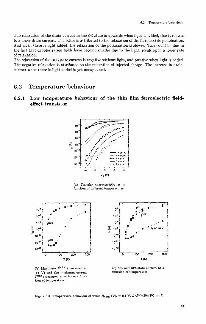
6.2. Temperature behaviour
The relaxation of the drain current in the ON-state is upwards when light is added, else it relaxes to a lower drain current. The latter is attributed to the relaxation of the ferroelectric polarization. And when there is light added, the relaxation of the polarization is slower. This could he due to the fact that depolarization fields have become smaller due to the light, resulting in a lower rate of relaxation. The relaxation of the OFF-state current is negative without light, and positive when light is added. The negative relaxation is attributed to the relaxation of injected charge. The increase in draincurrent when there is light added is yet unexplained.
6.2 Temperature behaviour
6.2.1 Low temperature behaviour of the thin film ferroelectric fieldeffect transistor
~ _o
10-6 ..... .... 10-7 •
lli 10'8 tMAX
10'9
10·10 !I
10-11 tMIN li .....•
10-12
0 100
....
•
10-6
10'7
10'8
~ 10-9 0
~ .. ~ ..-.;" ~ ~~· ;; "..-..... ,",. , .. .,.
// "" /" .... · ,/,/ ,." / ....... · '/ / ,,, .• . :·
.• j·' .:· - 10-10 / /:' . ·.
/ /l ••
/ j/ ,,'' -T=287K - I ~~ • • ------ T = 142 K 10·11
10·12
Î ..... ,. • • - - T = 61 K !" I •
\/ ,. --T=38K • • • T = 21 K
-4 -2 0 2 4
VG (V)
(a) Transfer charaderistic as a function of different temperatures.
• ··• 10-6
• . • .. ·· ... ·· ,•' 10'7
10'8
~ 10'9 _o
10·10
10·11
10·12
200 300 0
1oN_. :::I· :· .. · ···_ ... ·
I
... IOFF
• • . .. .... ·········· .• · IG at +4 V . . .. . ..
•••
100 200 300
T(K) T(K)
(b) Maximum JMAX (measured at +4 V) and the minimum current [MIN (measured at -4 V) as a runction of temperature.
(c) ON- and OFF-state current as a function of temperature.
Figure 6.3: Temperature behaviour of wafer Hthin (Vv = 0.1 V, LxW=20x300 pm2).
43

6. Light dependenee and temperature behaviour
Wafer Hthin was mounted on an Ie-holder and placed in the He-cryostat. The wafer was then caoled to a minimum temperature of 21 K. In the temperature range from room temperature to 21 K, several transfer characteristics were measured and depicted in figure 6.3(a). In figures 6.3(b) and 6.3(c) data deduced from the transfer characteristics are depicted, like the maximum current JMAX, the minimum current JMIN, the ON-state current J0 N, the OFF-state current JOFF and the gate leakage current measured at a gate voltage of +4 V. The transfer characteristic at room temperature has a ON/OFF-ratio of 3 and a MAX/MIN-ratio of about one orders of magnitude. At lower temperatures the transfer characteristics get slimmer and steeper resulting in a MAX/MINratio of 5 orders of magnitude at a temperature of 38 K. The gate leakage current decreases roughly logarithmically with a decrease in temperature. The minimum current JMIN decreases also down to a temperature of 80 K, where below JMIN is disturbed by the gate leakage current (,...., 40 pA). The ON- and OFF-state currents roughly decrease the same way when the temperature is getting smaller. The transfer charaderistics below 61 K show clockwise rotation, opposite of the ferroelectric rotation direction (counter clockwise). As the temperature decreases the number of charge carriers also decreases due to less thermal activation, resulting in a decrease in the maximum current. As the resistance increases the voltage drop across the ferroelectric insuiator decreases, resulting in non-saturized loop of the ferroelectric layer. This causes the transfer characteristics to become more slim and even the proper hysteresis rotation disappears. The observed hysteresis can be attributed to charge injection. Although the ferroelectric layer is swept in inner loops, there is enough charge displacement to deplete the channel to a difference in MAX- and MIN-state current of five orders of magnitude.
6.2.2 High temperature behaviour of charge displacement
The displaced charge as a function of temperature of a thin film as well as a bulk ferroelectric material have been measured. In case of the thin film ferroelectric material the gate leakage current becomes too high at temperatures above of 150 oe. This results in a non proper hysteresis measurement (not shown). For the bulk ferroelectric layer it is possible to perfarm hysteresis measurement, due to the absence of a gate leakage current (figure 6.4). Figure 6.4(a) shows that the displaced charge curve gets slimmer when temperature increases, and above 230 oe an almast linear relation between P and Va is observed. Figure 6.4(b) shows that the remnant polarization decreases from 0.35 ejm2 at room temperature to zero above 230 oe. The coercive field, Vc, also decreases to zero at the same temperature.
0.4
0.2
I o.o
-;:;?f; I ..-. I
:I I
-·.·_".'.6'.'.~:.:~.-;;·~-~~.;.:_:::~ ./. • /~. ~ ~::~c c..
·0.2
·0.4
·200
• •" ·········204°C
-284°C
200
(a) Charge displacement at measured at several temperatures.
0.4
I
• . ... .. -.. .. •.. .. .. .. ....... ···•• 0
~0.2 - .. • c..
• •• .•.... ···•·· 0.0 ~0~~10~0~~2700~~3~00~-4~0-0~
T(°C)
(b) Remnant polarization and coercive voltage vs. temperature.
Figure 6.4: Charg; displacement as a function of temperature measured at wafer A 8 uLKCf = 70 Hz, Cref = 56 nF, A = 0.18 mm ).
44

6.2. Temperature behaviour
Literature prediets the same behaviour as we abserve [20]. Above a temperature of 230 oe ( called the Curie-temperature) there is no net dipale moment in the ferroelectric material, which then becomes dielectric. Therefore it will result in an almast linear behaviour of displaced charge vs. applied field. The remaining hysteresis can be attributed to the presence of a possible series resistance, causing a phase shift of the signal measured at the reference capacitor. For PbZr0 _2Ti0_80 3 layers, the Curie-temperature is about 400 oe [20]).
6.2.3 High-temperature transfer characteristics
Figure 6.5 shows several transfer characteristics measured at wafer Athin at different temperatures, from room temperature up to 175 °C. The ON-state current increases with a factor of two in the temperature interval. The OFF-state current increases with three orders of magnitude. The transfer characteristics roughly maintain the same shape with the exception of the increase of drain-current at negative gate voltages ( due to an increae in gate current.
10'6
10'7 . I g I
_c 10'8 I I ., , .... .
10-9 , -- T= 23°C ··. ·. ·.) " T = 80 Oe .. ---I
·········T=11o 0c I " 10·10 I .. -T=175°c -," -4 4
Figure 6.5: Temperature dependenee ofwafer Athin (Vv = 0.1 V, LxW=5x300 J.tm2 ).
The sameexperiment as above has been performed at wafer Ethin· The maximum temperature to which the wafer is exposed, is about 330 oe. The shape transfarms the same way as is plotted in figure 6.5, even at a temperature of 330 oe there is proper hysteresis behaviour. The ON-state current increases with one order of magnitude between room temperature and 330 °C (not shown). Gate leakage current gets large and comparable with the drain current at temperatures above 250 °C. In figure 6.6 the gate current measured at Va = +5 V is depicted versus temperature. The figure shows that the gate current increases exponentially with temperature. After heating the wafer up to 330 oe, the wafer was exposed to room temperature without any slow cooling down of the wafer afterwards. At room temperature the semiconductor channel at the entire surface does not conduct. Hysteresis measurements at ferroelectric capacitors at the wafer only show a dielectric behaviour. We attribute the latter to too fast cooling down of the wafer, causing cracks in either the ferroelectric layer or semiconductor channel. The dielectric behaviour of the ferroelectric capacitor can be due to the creation of a dielectric layer of the semiconductor film or due to cracks in the ferroelectric layer itself. The increase in gate current is possibly due to defect conduction. When a leakage current flows through the insulator, it creates more defects, resulting in an increase in leakage current. That there is still hysteresis behaviour at 330 oe, is comprehensible, as the Curie temperature of PbZro.2Tio.s03 is about 400 oe [20].
At wafer Hthin transfer characteristics are measured as a function of temperature (see figure 6.7). The characteristics are measured befare the wafer is heated. After being exposed to a temperature of 200 ° C, the wafer is caoled down slowly ("" 2 hours). Then, again the transfer characteristic is measured. The figure shows that, after the heating process, the current at Va = +4 V is smaller than the ON-state current with 1 order in magnitude and becomes even negative when Va is larger
45
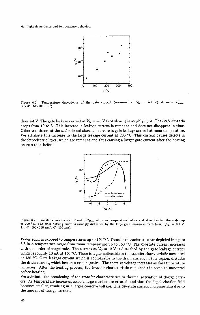
6. Light dependenee and temperature behaviour
10'6 • • • •
~ 10'7 • -"
• 10'8
• 0 100 200 300 400
T (oC)
Figure 6.6: Temperature dependenee of the gate current (measured at Va (LxW=10x300 J.Lm2 ).
+5 V) at wafer Ethin·
than +4 V. The gate leakage current at Va= +5 V (not shown) is roughly 5 J.LA. The ON/OFF-ratio drops from 10 to 3. This increase in leakage current is remnant and does not disappear in time. Other transistors at the wafer do not show an increase in gate leakage current at room temperature. We attribute this increase to the large leakage current at 200 oe. This current causes defects in the ferroelectric layer, which are remnant and thus causing a larger gate current after the heating process than before.
-4
; ~
I .,.
I _, / - - before heating - after heating
4
Figure 6.7: Transfer charaderistic of wafer Hthin at room temperature before and after heating the wafer up to 200 °C. The after heating curve is strongly disturbed by the large gate leakage current (~A). (Vv = 0.1 V, LxW=lOOx300 J.Lm2 , G=105 pm).
Wafer Fthin is exposed to temperatures up to 150 oe. Transfer characteristics are depicted in figure 6.8 in a temperature range from room temperature up to 150 oe. The ON-state current increases with one order of magnitude. The current at Va = -2 V is disturbed by the gate leakage current which is roughly 10 nA at 150 oe. There is a gap noticeable in the transfer characteristic measured at 150 oe. Gate leakage current which is comparable to the drain current in this region, disturbs the drain current, which becomes even negative. The coercive voltage increases as the temperature increases. After the heating process, the transfer characteristic remairred the same as measured befare heating. We attribute the broadening of the transfer characteristics to thermal activation of charge carriers. As temperature increases, more charge carriers are created, and thus the depolarization field becomes smaller, resulting in a larger coercive voltage. The ON-state current increases also due to the amount of charge carriers.
46

6.2. Temperature behaviour
_o 10-10
-2
-T=21°C
""'T=100°C -T=1so•c
2
Figure 6.8: Temperature dependenee ofwafer Fthin (Vv = 0.1 V, LxW=10x250 p.m2).
6.2.4 High temperature behaviour of the bulk ceramic transistor
In figure 6.9 transfer characteristics measured at the temperature interval between room temperature and 350 oe are depicted. The ON-state current at a temperature of 119 oe is reduced with a factor of three compared the curve at room temperature. The coercive voltage also has become smaller withafactor of 2.3 {from 70 V to 30 V). The curves at 24 oe and 119 oe show a counter clock wise rotation while the other two {162 oe and 350 oe) rotate clock wise. The curve at 350 oe shows almast no hysteresis. When the wafer is caoled down, the transfer characteristic reproduces as measured befare the heating cycle.
-- T=119°C -T=162°C
--- T=3so•c
-200 -100 0 100 200
VG(V)
Figure 6.9: Transfer charaderistic at several temperatures with wafer CsuLK (Vv = 0.1 V, LxW=25x250 p.m2). Note that the 24 oe and 119 oe curves rotate counter-clockwise and the 162 oe and 350 oe curves rotate clockwise.
When the temperature is increased to 119 oe, the polarization is getting smaller as shown in figure 6.4{b) where the polarization vs. the temperature is depicted. Therefore resulting in a smaller ON-state current and larger OFF-state current. The drain current is proportional to the displaced charge, Iv ,....., !lQ. In figure 6.4(b) the reduction in remnant polarization (from 0.34 to 0.22 ejm2
)
is roughly by a factor of 1.5 between room temperature and 119 oe, while the difference in drain current {57 and 13 J.LA) is roughly by a factor of 4. That these two values do nat correspond is probably due to the fact that the mobility in bath cases is nat constant. The reduction in coercive voltage {from 70 V to 30 V) is proportional to the reduction in coercive voltage {from 140 V to 70 V) measured in the hysteresis measurement (see figure 6.4{b)). Above the eurie-temperature (in this case 230 oe) the ferroelectric behaves like a dielectric, thus resulting a no hysteresis behaviour at a temperature of 350 oe with the exception of a small hysteresis behaviour due to injected charge. Although there is a ferroelectric hysteresis behaviour at 162 oe as shown in figure 6.9, the curve
47

6. Light dependenee and temperature behaviour
exhibits a clockwise direction of rotation. We attribute this phenomenon to charge injection. The injected charge exceeds in this case the polarization of the ferroelectric insuiator causing the actual drain-current at Va < 0 V to be larger than the drain current at Va > 0 V. Relaxation experiments show that the OFF-state current decreases in time and the ON-state current increases, just as expected in charge injection relaxation measurements (not shown).
6.3 Summary and discussion
The amount of charge carriers in the semiconductor channel of field-effect transistor can be increased by either adding light causing charge carriers to be excited in the conduction band, or by increasing the temperature causing thermal activation of charge carriers. When the amount of charge carriers increases, the depolarization field decreases, causing the coercive voltage to increase. When light is added the ON-state current only changes within a factor of 2, which is small compared to the ON/OFF-ratio (normally larger than 2 orders of magnitude). We have shown that a large difference in the maximum and miniurn current can be obtained, if we adjust the amount of charge carriers in the semiconductor channel, in this case by lowering the temperature to 40 K. At high temperatures up to 300 oe, the gate leakage current becomes so high in a transistor with a thin-film insulator, that defects are created in the insuiator which are non-reversible. A bulk insuiator shows no leakage current. Thus using a bulk ferroelectric insuiator makes the device operational even for temperatures up to the Curie temperature (400 oe for PbZr0.2Ti0.80 3 ). A disadvantage of a thicker insuiator is that the voltage necessary to switch the device also increases.
48

Chapter 7
Relaxation of the channel cond u etanee
Knowledge of the retention time of a memory state is important for memory application. Therefore we will investigate the stability of the channel conductance for the ON- and OFF-state. Also the time-evolution of the channel conductanceis stuclied as function of different applied voltage pulses.
7.1 Thin film transistors with a ferroelectric insuiator
The time evolution of the drain current is depicted in figure 7.1, for the ON-state as well as the OFF-state. The channel is pulsed with a voltage pulse of 6 V and pulse width of 1 s. The figure shows that the logarithm of the ON-state current slowly decreases linear with the logarithm of time (roughly 16 % per decade). The logarithm of the OFF-state current increases with the logarithm of time (roughly 60 % per decade). The ON/OFF-ratio at t = 50 s is roughly 700 and after 104 s it is reduced toa ratio of roughly 170. Extrapolating the curves, the two curves would interseet after roughly 109 s (:::::: 30 years). This time-scale is huge and therefore it is more of interest after what time-scale the ON-OFF-ratio is reduced to 10. Extrapolating the curves, this time-scale is roughly 107 s (:::::: 100 days).
_o
1 o·9 L....~.......,,.........~"'-:-~ ........ ..,.....~"""= 101 102 103 104 105
t(s)
Figure 7.1: Time evolution of the drain current measured at wafer Cthin (pulse height = 6 V, pulse width = 1 s, Vv = 0.1 V, LxW=20x300JLm2 , G=16JLm).
In figure 7.2 the time evolution of the drain current is depicted for different voltage pulses applied to the gate electrode with different pulse heights (between 3 and 5 V). To measure the time evolution of the ON-state, the channel is first pulsed into the OFF-state, whereafter a positive voltage pulse is applied to the gate electrode. Then the drain-current of the ON-state is measured. The same
49

7. Relaxation of the channel conductance
action is repeated for the time evolution OFF-state. The figure shows that the ON-state current pulsed with a pulse height of 3 V decreases in time, while the ON-state currents pulsed with a pulse height of 4 and 5 V first increase and then decrease in time. For the OFF-state current, pulsed with a pulse height of 3.5 V, the current first decreases for a short time whereafter it increases. For a pulse height of 4 V the OFF-state current first increases whereafter it increases, only with a smaller slope than the 3 V curve. For a pulse height of 5 V only a decrease in the OFF-state current is observed. We attribute the increase in drain current in the ON-state to the relaxation of injected charge (see theory section 2.7). Once the charge is relaxed, the current decreases due to relaxation of the polarization of the ferroelectric materiaL The decrease in current when a voltage pulse of 3 V is applied, is caused by the fact that this voltage is too small to inject charge in the ferroelectric layer. The decrease in the OFF-state current can also he attributed to charge injection. When the voltage pulse increases, it will cause more injected charge in the ferroelectric layer. Thus the relaxation of the injected charge will take more time. Therefore the increase in current starts for the 3.5 V pulse after roughly 30 s, while for the 5 V pulse no increase is observed after roughly 500 s.
7.0
~ 6.6
l -
0 0.2
relaxatlon of lnjected
lr~ 0.1 ~
·5.0
3.0
relaxation of ferroelectrtc 71arlzation
1: •:I : :::::: :1 I
o.oL.....Lo-~-.... so~o=--~-1o-='"o __ o_,...__.,
t (s)
Figure 7.2: Time evolution of the drain current with different applied voltage pulses, measured at wafer Athin (pulse width = 1 ms, Vv = 0.1 V, LxW=20x300 JLm 2 , G=16JLm).
7.2 Transistors with a bulk ferroelectric insuiator
At wafer Cs u LK the time evolution of the ON-state and OFF-state current has been determined during 105 s (roughly 1 day). Figure 7.3 shows the time evolution of the drain-current of both states. The OFF-state remains nearly constant and after 5 104 s there is an sudden increase in current. The ON-state shows a linear decrease with the logarithm of time ("' 20 % per decade). We attribute the decrease in ON-state current to the relaxation of the polarization. However the behaviour of the OFF-state current is not understood. It is expected to increase due to the relaxation of the ferroelectric layer, but it remains constant for 3 104 s.
In figure 7.4(a) the time evolution of the ON-state current is depicted after several voltage pulses are applied (between 100 V and 150 V). First the channel was pulsed in the OFF-state with the same pulse height, whereafter the channel was pulsed into the ON-state. The figure shows that the ON-state current remains constant for roughly 50 s whereafter it decreases linearly with the logarithm of time. The slope of the decreasing part of the curves is nearly the same for all the different applied voltage pulses. In figure 7.4(b) the time evolution of the channel conductanceis depicted. The OFF-state current remains constant for 100 s whereafter it increases linearly with the logarithm of time. The slopes of the curves are nearly constant for the different applied voltage pulses. The behaviour of the ON-state current after 100 s is attributed to the relaxation of the ferroelectric
50

7.3. Summary and discussion
------t(s)
Figure 7.3: Time evolution of drain current measured at wafer CBULK (Vpulse LxW=10x150pm2 ).
150 V, r 999 ms,
polarization and is the same for different kind of voltage pulses. The constant drain current before 100 s, can be attributed to charge injection. The injected charge causes the drain current to be lower in the ON-state. After a time of 50 s the injected charged is relaxed, whereafter the current decreases. The sameargument applies for the OFF-state current.
70
......... 130V • • • 120 V -110V -- 100V
100
1 (s)
(a) ON-state relaxation
10
l 8
_o
6
--150V ------140V ......... 130V
• • • 120 V -110V
, ,
__ ... /· ,
-- 100:.......... /.· ---- / •·· / ....... _________ • _____ .. ______ ......... -- •• .-!::
............
10 100
I (s)
1000
(b) OFF-state relaxation
Figure 7.4: Time evolution of drain current measured at wafer CBULK for different applied voltage pulses (pulse width 999 ms, LxW=12x250 pm).
7.3 Summary and discussion
The retention time of a memory state for the thin film transistor is roughly 107 s. The retention time for the bulk ferroelectric transistor is larger than 105 s. Ref. [2] showed for bulk ferroelectric devices a retention time smaller than 104 s. After this time the ON-state current was equal to the OFF-state current. The cause of the difference between the two retention times of the bulk ferroelectric devices is unknown. Charge injection has been observed but for the thin film transistor as well as the bulk ferroelectric transistor the infiuence of injected charge is small ( < 5 %); this in contrast to fioating gate devices which operate due to the phenomenon of charge injection.
51

7. Relaxation of the channel conductance
52

Chapter 8
Field-effect mobility and subthreshold behaviour
Knowledge of the field-effect mobility of the semiconductor layer is important, as it limits the maximum conductance of the transistor channel. In this chapter we will discuss the field-effect mobility measured with the differential methad as explained insection 3.2.7, fortransistors with a thin film as well as a bulk ferroelectric insulator. The field-effect mobility can also be obtained in a non-differential way, using the fact that the channel conductanceis a function of the field-effect mobility and the displacèd charge. This relationship also involves the subthreshold regime.
8.1 Thin film field-effect transistors with a ferroelectric insulator
To measure the field-effect mobility according to equation 2.12, we have to measure the gate capacitance, Ca, and the transconductance, 9m· Using a frequency sweep of the capacitance measurement as well as the transconductance measurement, we will obtain the frequency band in which the gate capacitance and transconductance correctly are measured. Then with a gate voltage sweep bath quantities are measured as a function of the gate voltage resulting in a calculated mobility as a function of the gate voltage.
In capacitance measurements, resistances in the circuit are always influencing the measurement invalving RC-times, which limits the frequency band. We will apply a gate bias voltage of -4 V in order to obtain the highest channel resistance. Figure 8.1 shows bath measurements. Inthetwo-points measurement a bias voltage and oscillating voltage of 0.3 V (rms) is applied. The large oscillating voltage is necessary to obtain a signific output from the impedance analyzer. In panel (a) the real part and the imaginary part of the measured admittance are depicted as a function of the frequency. The imaginary part equals wC, in other words the imaginary part is proportional to the gate capacitance. Below frequencies of 50Hz the real part and imaginary part pass through each other. Between 50Hz and 200Hz the imaginary part is larger than the real part. The slopes of the imaginary part and real part in this interval are roughly 1 and 2 in this log/log plot. At 100 Hz the imaginary part of the admittance yields 10-7 S. Between300Hz and 7 kHz the real part of the admittance exceeds the imaginary part, whereafter the imaginary part increases with a slope of roughly 1 in a log/log plot. The noisy behaviour of the admittance below 50 Hz is due to the fact that the impedance analyzer is nat capable of measuring the admittance with a signific output in this frequency range. In the range between 50 Hz and 200 Hz the admittance behaves like the admittance of a capacitor C ( ....... 0.3 nF) placed in series with aresistor R ( ....... 10 MO). The admittance Y of such a circuit, yields:
w2C 2R + jwC y = -----:::-=:::....."."-
1 + w2R2C2 (8.1)
53

8. Field-effect mobility and subthreshold behaviour
§: >-
10·6 H
~i' 10-7 . ;
, -Re(Y)
10'8 -- lm(Y)
101 102 103 104 105
I (Hz)
(a) Admittance of a two-points measurement in order to measure the gate capacitance; the bar indicates the frequency interval in which the gate capacitance can he measured.
(b) Admittance of a three-points measurement in order to measure the transconductance. The arrow indicates the frequency interval in which the transconductance can he measured.
Figure 8.1: Gate capacitance measurement and transconductance measurement at a transistor at wafer Athin at a gate bias voltage of -4 V.(!= 100Hz, Vn = 1 V, Vosc = 0.3 V, LxW=100x300flm2 , G=105flm).
We see that when w < (RC)-1 that the imaginary part vs. frequency holds a linear dependenee (slope of 1 in a log/log plot) while the real part shows a square behaviour (slope of 2 in a log/log plot). The measured capacitance per square at a frequency of 100Hz (0.01 C/m2
) roughly equals other measurements at PbZr0 .49Ti0 .51 0 3 capacitors with metal electrades [13]. Above a frequency of 7 kHz the imaginary part increases again, we attribute this to a parasitic capacitance ( .....,g pF). Therefore we can conclude that in the frequency interval between 50 Hz and 200 Hz the gate capacitance can be accurately determined. This interval is plotted with a bar in panel (a).
In Panel (b) the admittance is determined in the three points measurement. An oscillating voltage with a bias voltage (-4 V) is applied at the gate electrode and at the drain electrode a voltage of 1 V is applied. The real part of the admittance shows a little increase in the frequency interval up to 200 Hz, whereafter the imaginary part becomes roughly equal to the real part and exceeds the real part after 10 kHz. The little increase up to 200Hz is attributed to the slow filling of trap states. When the frequency increases, these trap states cannot be filled resulting in a higher conductance. At higher frequencies the real part is disturbed by the imaginary part which roughly equals the measured capacitance in panel (a). We can conclude that in the frequency up to 200Hz, the transconductance is correctly measured. Above 200 Hz, the transconductance is disturbed by the real part of the admittance measured in the gate capacitance measurement.
We have determined the frequency at which the gate capacitance as well as the transconductance has to he measured, namely between 50 and 200 Hz. In the gate voltage sweep measurement we choose 100 Hz for the frequency. The gate voltage is swept from a negative bias to a positive bias and back again. In figure 8.2 the gate capacitance as well as the transconductance are depicted. In panel (a) the gate capacitance and the real part of the admittance are depicted. The real part is smaller than the gate capacitance by a factor between 3 and 10. The gate capacitance is roughly constant and shows two peaks, and each peak is positioned at the coercive voltage of the ferroelectric materiaL The same curve has been observed by Ref. [13]. Panel (b) shows the transconductance vs. the bias gate voltage. The imaginary part is a bout one order smaller than the transconductance. From -4 V the transconductance increases slowly and
54

§: >-
8.1. Thin film field-effect transistors with a ferroelectric insuiator
~ ~ ~,. ______ _,..",._-_ ... __ .A.
•1\o' ,
(a) Gate capacitance measurement.
-4 4
(b) Transconductance measurement.
Figure 8.2: Gate capacitance measurement and transconductance measurement at a transistor at wafer Athin· The arrows indicate the rotation direction as the gate voltage is swept. (Same parameters as in tigure 8.1).
0 '1 '--_-'-4~--2'--~--'o-~_._2~-4L-.J
VG(V)
Figure 8.3: Field-effect mobility vs. gate voltage measured at wafer Athin· The arrows indicate the rotation direction as the gate voltage is swept (Same parameters as in tigure 8.1).
at +1.5 V the transconductance suddenly increases with a factor of 7 and starts to decrease after this peak. From a positive gate voltage to a negative gate voltage the transconductance increases and drops at -1.5 V whereafter it coincides with the other curve.
The increase after a gate voltage of +2 V can have two causes. Firstly, when there is a contact resistance present and the channel is brought into accumulation, the transconductance is limited by the conductance of such a contact resistance. The real transconductance of the channel becomes larger as the gate voltage increases. But because the contact resistance is independent of the gate-voltage, the transconductance will tend to zero. Secondly, when there is charge injection present, more charge will he injected as the gate voltage increases. This results in a decrease in transconductance as there are less charge carriers available. However there is no peak observed at a negative gate voltage. lt is unlike that in this case only charge injection occurs at positive voltages. The minimum resistance in the transfer characteristic is roughly 15 kn, which is roughly equal to the determined contact resistance (see section 4.4). From the transfers characteristic (not shown) the charge injection is roughly 20 % at positive applied voltages and a factor of 5 at negative voltages. The absence of a peak in the transconductance measurement at negative gate voltages and the
55

8. Field-effect mobility and subthreshold behaviour
fact that the minimum resistance is roughly equal to the contact resistance, sustain the statement that the transconductance at positive gate voltages (Va > 2 V) is limited by a contact resistance.
In figure 8.3 the field-effect mobility calculated with equation 2.12 is depicted. As the gate capacitance measurement showed a nearly constant behaviour, the mobility curve resembles the transconductance curve. We abserve a mobility of maximum 2 cm2 JVs and a minimum mobility of 0.2 cm2 /Vs. The maximum mobility is in good agreement with the Hall-mobility measured in Hall measurements [7] which is roughly 2 cm2 /Vs.
8.2 Field-effect transistors with a bulk ferroelectric insulator
To measure the mobility fora bulk ceramic transistor the sameapproach is used as mentioned in the previous section. First the correct frequency interval (50,...,.,400 Hz) was determined with a frequency sweep. Then with a gate voltage bias sweep, the gate capacitance and the transconductance are measured. Combining the two results with equation 2.12 gives the field-effect mobility which is plotted in figure 8.4 fora transistor at wafer CBuLK·
The maximum field-effect mobility is roughly 3 cm2 /Vs, while the minimum mobility yields 0.08 cm2 /Vs. Note that the curve in the figure resembles with the curve in figure 8.3. At wafer BBuLK the measurement is also performed, resulting in a mobility between 0.3 and 2 cm2 /Vs.
Figure 8.4: Field-effect mobility vs. gate voltage measured at wafer Cs u LK. (! LxW=25x250J.Lm2 ).
100 Hz, Vosc = 4 V,
Using the transfer characteristic we can obtain the minimum channel resistance, which is about 8 kD. The contact resistance (see section 4.4) is 2 kD. The transconductance measurement (not shown) showed for positive gate voltages and for negative voltages a peak. As the channel resistance is higher than the contact resistance, we attributed these two peaks to the charge injection. This results also in two peaks in the calculated mobility versus gate voltage.
Asthere could he charge injection present, sweeping at inner loops would result that the charge injection is less. Therefore insteadof sweeping up to 150 V, we applied a maximum gate bias voltage of 70 V. In figure 8.5(a) the mobility is depicted. lt does not show any peaks as in the previous measurements. In figure 8.5(b) the mobility is depicted against the displaced charge measured with a Sawer-Tower circuit (f = 200Hz, Cref = 56 nF). The two curves, i.e., the forward sweep and the backward sweep coincide. Hall measurements [21] with a 30 nm In20 3:Sn layer with the same doping concentration on a epitaxial PbZro.2Tio.sÜ3 layer yield a larger value for the mobility (8 cm2 /Vs). We attribute this to the fact that the ceramic bulk material is porous. Therefore the contact areas of grains in the semiconductor layer are smaller, which results in more scattering, yielding a smaller mobility.
56
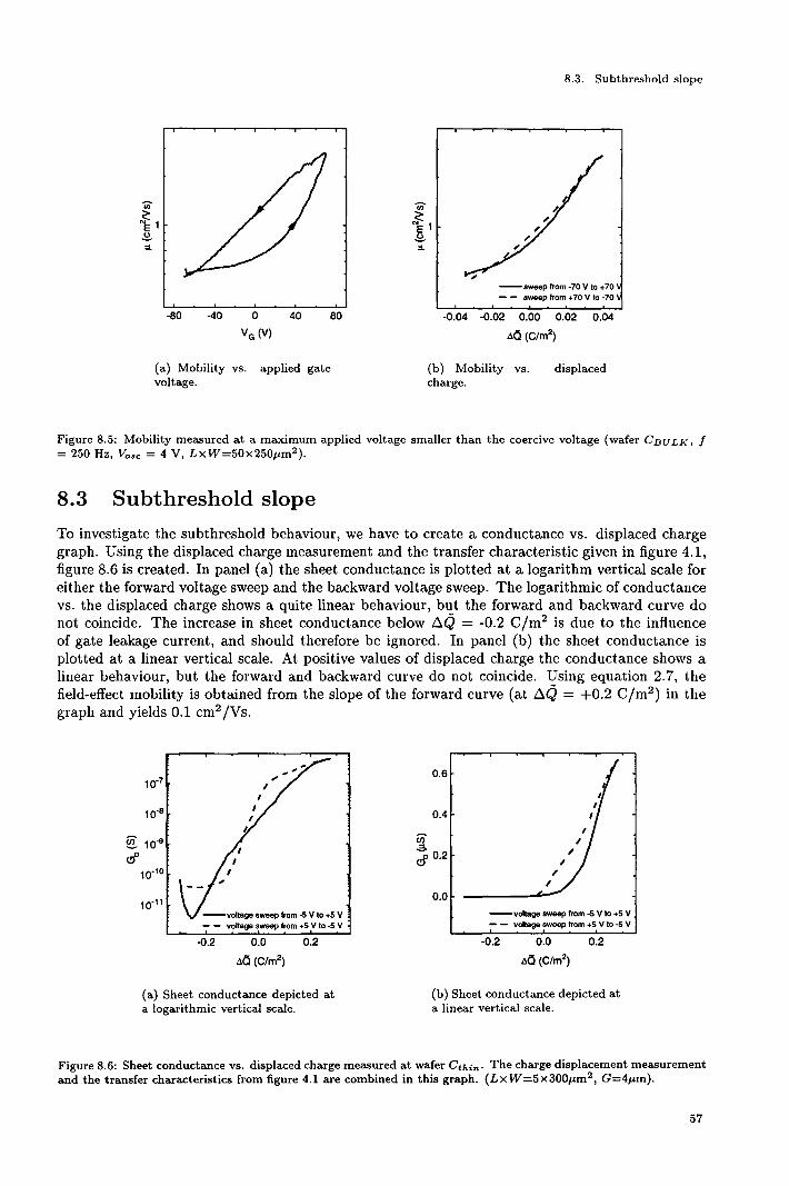
(a) Mobility vs. applied gate voltage.
8.3. Subthreshold slope
--sweep trom ·70 V to +70 -- sweep from +70 V to -70
-0.04 -0.02 0.00 0.02 0.04
aö (C/m2)
(b) Mobility vs. charge.
displaced
Figure 8.5: Mobility measured at a maximum applied voltage smaller than the coercive voltage (wafer CBu LK, f =250Hz, Vosc = 4 V, LxW=50x250pm2 ).
8.3 Subthreshold slope
To investigate the subthreshold behaviour, we have to create a conductance vs. displaced charge graph. Using the displaced charge measurement and the transfer characteristic given in figure 4.1, figure 8.6 is created. In panel (a) the sheet conductanceis plotted at a logarithm vertical scale for either the forward voltagesweepand the backward voltage sweep. The logarithmic of conductance vs. the displaced charge shows a quite linear behaviour, but the forward and backward curve do not coincide. The increase in sheet conductance below ~Q = -0.2 Cjm2 is due to the infiuence of gate leakage current, and should therefore he ignored. In panel (b) the sheet conductance is plotted at a linear vertical scale. At positive values of displaced charge the conductance shows a linear behaviour, but the forward and backward curve do not coincide. Using equation 2.7, the field-effect mobility is obtained from the slope of the forward curve (at ~Q = +0.2 Cjm2 ) in the graphand yields 0.1 cm2 /Vs.
--voltage sweep from -5 V to +5 V - - voltage sweep trom +5 V to -5 V
-0.2 0.0 0.2
aö (C/m2)
(a) Sheet conductance depicted at a logarithmic vertical scale.
0.6
0.4
~ d' 0.2
0.0
--voltage swaep from -5 V to +5 V - - voltage swaep from +5 V to -5 V
-0.2 0.0 0.2
aö (C/m2)
(b) Sheet conductance depicted at a linear vertical scale.
Figure 8.6: Sheet conductance vs. displaced charge measured at wafer Cthin· The charge displacement measurement and the transfer characteristics from tigure 4.1 are combined in this graph. (LxW=5X300pm2 , G=4pm).
57

8. Field-effect mobility and subthreshold behaviour
The observed behaviour is in good agreement with the theory section 2.6. For a negative charge displacement we abserve a exponential relationship between the channel conductance and the displaced charge, while for a positive charge displacement the channel conductanceis proportional to the charge displacement.
In figure 8. 7 a similar measurement is depicted. The charge displacement is measured at a MISdiode (200x200J.tm2 ) with a Sawyer-Tower circuit (f =90Hz, Cref = 56 nF), while the transfer characteristic is measured using a drain voltage of 0.1 V and a frequency of 0.03 Hz. The sheet conductance vs. displaced is depicted, the outer loop is measured with a gate voltage amplitude of 4 V while the inner loop is measured with a gate voltage amplitude of 2 V. Panel (a) shows that the slope of the forward and backward curve are roughly the same, but in panel (b) the forward loop coincides with the backward loop at a positive amount of displaced charge. From the slope (at D..Q = 0.1 Cfm2 ) the field-effect mobility yields 0.9 cm2 /Vs. We attribute the horizontal shift between the forward and the backward curve in both figures to charge injection. For example, at a negative charge displacement, positive charge carriers are injected into the ferroelectric layer. This results in an increase in channel conductance. At a positive charge displacement, the injected charge relaxes and now negative charge carriers are injected in the insulator, causing the conductance to be smaller than the conductance in case there is no charge injection.
-0.1 0.0 0.1
AÖ (C/m2)
(a) Sheet conductance vs. displaced charge at a logarithmic vertical scale.
20
15
~ 10 0
(!)
5
0
-0.1 0.0 0.1
AO (C/m2)
(b) Sheet conductance vs. displaced charge at a linear vertical scale.
Figure 8.7: Sheet conductance vs. displaced charge measured at wafer Athin· The outer loop is obtain measuring with a gate voltage amplitude of 4V, while the inner loop is obtained with a gate voltage amplitude of 2V (LxW=lOOx300J.tm2 , G=95J.!m2 ).
In figure 8.6 and in figure 8.7 the field effect mobility is determined to 0.1 cm2 /Vs and 0.9 cm2 /Vs, respectively. As the semiconductor layer has the same thickness and composition, the difference is rather large. However, the lower mobility is measured on a transistor with a shorter souree-drain length (5 nm) than the transistor with a higher mobility (100 nm). We now will show that this is caused by a series resistance or a contact resistance. With Go = J.t!::l.Q (equation 2.7), the mobility is obtained. The sheet conductance Go,calc, is calculated using the meaured conductance Grneas and the geometry of the device:
L Go,calc = W Grneas• (8.2)
The redprocal of the measured conductance is related to the real sheetresistance of the channel
58

8.4. Summary and discussion
Ro,chan and any other series resistance Rseries (including a contact resistance):
-1 L Gmeas = W Ro,chan + Rseries · (8.3)
Thus the calculated sheet conductanceis related to (equation 8.2):
L [ L ] -1
Go,calc = W WRD,chan + Rseries
(8.4)
= [ w ]-1
Ro ,chan + L Rseries
The last equation shows that when L increases the term with Rseries decreases. This results in an increase in the calculated sheet conductance and therefore an increase in the mobility. In our case the series resistance also depends on the souree-drain length, as a part of the channel which is nat covered by the gate increases from 1 J.Lm to 5J.Lrn. However the increase in channel length is a factor of 20, and this results always in a increase of the calculated sheet conductance and therefore an increase in mobility.
In figure 8.8 the same measurement is repeated. Charge displacement and transfer characteristic are measured at the same frequency. The measured frequency is 1 Hz, as at higher frequencies the gate switching current is disturbing the channel conductance measurement. The charge displacement is measured with a Sawyer-Tower circuit (Cref = 1 Hz), while the channel conductanceis measured by a voltage drop over a reference resistance of 330 n. The same behaviour is observed as in the previous figure. Charge injection causes a shift in the two curves. From the slope the field-effect mobility yields 2.8 cm2 /Vs, which is similar to the differential measured mobility. This value is nat limited by the presence of a contact resistance ( .....,2 kn, see section 4.4), as the minimum channel resistance is roughly 10 kn.
§: 10"5
ei"
10-6 '--~--'--~--'--~--'--...___, -0.2 0.0 0.2
aö (C/m2)
(a) Sheet conductance depicted at a logarithmic scale.
60
I I
40 I I
§: , D ;
Cl 20 I I
I
0
-0.2 0.0 0.2
aO (C/m2)
{b) Sheet cond u etanee depicted at a linear scale.
Figure 8.8: Sheet conductance vs. displaced charge measured at wafer CsuLK (f = 1 Hz, Cref = 330 !1, R.,..f = 330 !1, Vv = 1 V, LxW=150x250pm2 ).
8.4 Summary and discussion
We showed that the calculated field-effect rnahilities are limited in case of the thin film transistor (J.L = 2 cm2 JVs) by a contact resistance and in case of the bulk ferroelectric transistor
59
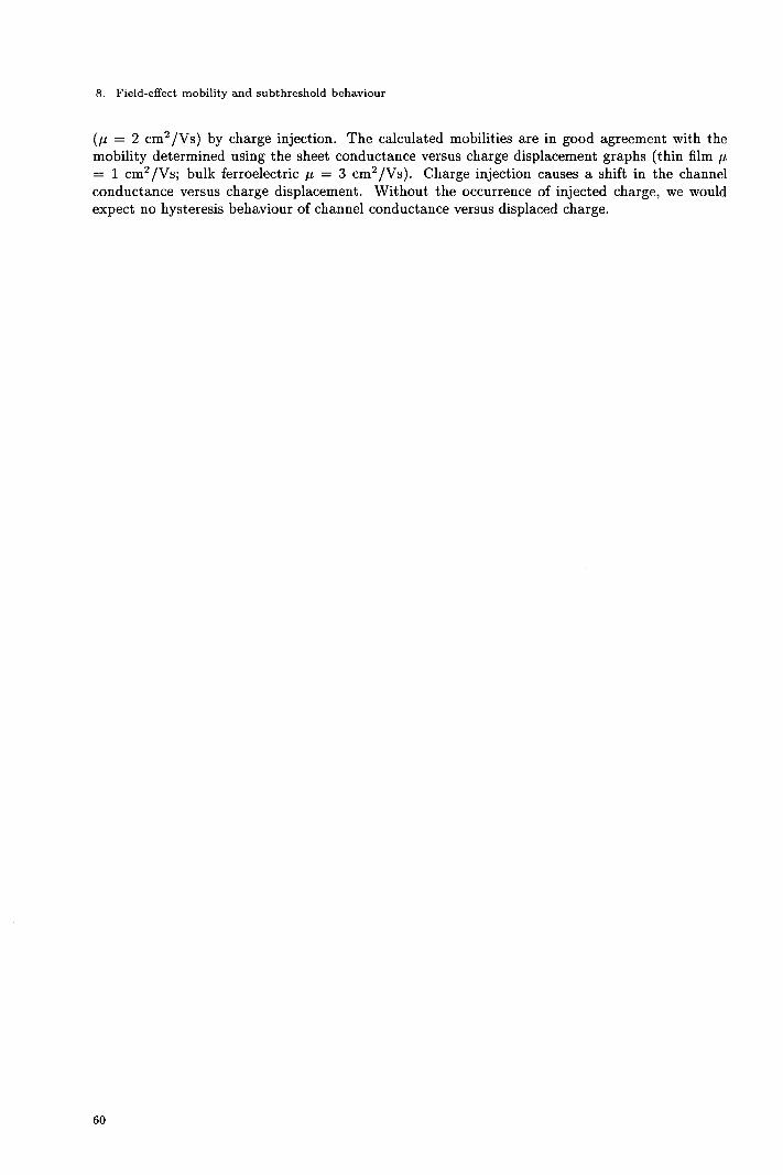
8. Field-effect mobility and subthreshold behaviour
(t-L = 2 cm2 /Vs) by charge injection. The calculated rnahilities are in good agreement with the mobility determined using the sheet conductance versus charge displacement graphs (thin film 1-L
= 1 cm2 /Vs; bulk ferroelectric 1-L = 3 cm2 /Vs). Charge injection causes a shift in the channel conductance versus charge displacement. Without the occurrence of injected charge, we would expect no hysteresis behaviour of channel conductance versus displaced charge.
60

Chapter 9
Conclusions
In this report we presented the electrical characteristics of several field-effect transistors, the most important being an operating depletion-type thin-film field-effect transistor with a ferroelectric insulator. The remnant polarization of the ferroelectric insuiator causes the channel to be fully depleted, resulting in a difference in resistance of nearly four orders of magnitude between channel depletion and non-depletion. A few concepts arise in this report overlapping the different chapters and therefore they will be discussed here.
The depletion of the transistor channel can be influenced in a few ways. Increasing the doping concentration and the thickness of the semiconductor channel, or increasing the environment temperature, cause the channel to contain too much charge for depletion. In the case that the amount of charge carriers is low, the ferroelectric material is influenced by a depolarization field, which can be reduced by increasing the light intensity or the environment temperature. The maximum conductance is limited by the field-effect mobility and the maximum charge displacement. The minimum conductanceis limited by the charge displacement of the insuiator and the depolarization field. In order to lower the minimum conductance, either the charge displacement has to increase or the depolarization field compared to the coercive field has to be reduced. The first can be done by using other ferroelectric materials with a larger charge displacement. The influence of a depolarization field can be reduced by either increasing the insuiator thickness or reducing the semiconductor thickness.
Charge injection causes a reduction of induced charge in the semiconductor channel. Pulse measurements show that the amount of injected charge increases as the applied gate voltage increases. Relaxation measurements show also the occurrence of charge injection. The injected charge influences the channel conductance by an amount smaller than 5% for the ON-state current, and for the OFF-state current by an amount smaller than a factor two. Endurance measurement show that the infiuence of injected charge for the ON-state current increases to a factor of 2 in channel conductance, due to the fact that the channel resistance is langer camparabie to the contact resistance. At higher temperatures we observed for the transistor with a bulk ferroelectric layer, that charge injection is dominating the field-effect, while the polarization decreases. The field-effect of charge injection is similar to the field-effect in floating gate devices.
The presence of a possible contact resistance between the mobyldenum contact pads and the semiconductor layer, has been shown in a few experiments; first of all, by variation of the length of the semiconductor channel. Secondly, by camparing the transfer charaderistics using a four-points measurement or a two-points measurement. Pulse measurements show no-charge injection for ONstate current, when the ON-state resistance is comparable to the contact-resistance. The measured field-effect mobility turnes out to be smaller than the real mobility when there is a contact resistance present. This contact resistance is due to a BaZr03 capping layer between the contact pad and the semiconductor channel.
61

9. Conclusions
We have shown that the life-time of the device can be reduced in two ways. First, the device is sensitive to repeated switching, and shows a crucial fatigue behaviour after 106 switching cycles. Secondly, gate leakage currents cause irreversible defects in the thin film ferroelectric insuiator at high temperatures (> 200°C); this in contrast to the bulk ferroelectric transistor which is not affected by exposing to high temperatures. To solve the first problem, further research has to clone to investigate the degradation mechanism of the semiconductor layer. If operation at high temperatmes using a thin film ferroelectric device is needed for applications, new ferroelectric materials with lower leakage currents have to be investigated.
For future directions the following remarks are made. Other deposition methods could be considered, as pulsed laser deposition is not suitable for real production. The preliminary investigation using a spun Sn02 semiconductor layer showed promising results. A large difference between the minimum and maximum resistance ( ....... 105 ) was observed. If operation at high temperatures of the thin film ferroelectric transistor is necessary for applications, the ferroelectric insuiator should be improved to reduce gate leakage currents. When the operation of the device is necessary at a bias gate voltage, the maximum resistance can be increased if another insuiator with smaller leakage currents is used. To obtain a larger ON-state conductance, first the contact resistance has to be eliminated, and the mobility of the semiconductor layer should increase. Therefore further research has to be clone to investigate new semiconductor materials and the deposition methad has to be reconsidered; this, because the semiconductor layer is consisting out of grains which are limiting the mobility. Increasing the grain size, should result in a higher mobility.
9.1 Acknowledgments
My graduation professor J .H. Wolter is acknowledged for giving me the oppurtunity to perfarm my graduation project at Philips Research Laboratories. I am indebted toMennoPrins for his continous enthousiastic mentorship, to the memhers of the New Oxidic Thin Film project Hans Cillessen, Ben Giesbers, and Harry van Esch, besides wafer preparation, for their abundant material- and processing knowledge. I would like to thank my fellow students at Philips for giving my stay a more student-like character: Bas Hendriksen, Benoit Lemonnier and Diederik B.A. Rep. The latter, tagether with M. Kerskes, is thanked fortheir enthousiastic and challenging discussions about physical as well as non-physical matters.
62
References
[1] J.L. Moll and J. Tarui, A new solid state memory resistor, IEEE Trans. Electron Devices ED-10, pp. 338-339 (1963)
[2] J.C. Crawford and F.L. English, Gemmie Ferroelectric Field Effect Studies, IEEE transactions on electron. devices, ED-16 6, pp. 525-532 (1969)
[3] S.Y. Wu, Memory retention and switching behavior of metal-ferroelectric-semiconductor transistors, Ferroelectrics 11, pp. 379-383 (1976)
[4] J.F.M. Cillessen, Pulsed laser deposition of oxidic films, thesis University of Twente, the Netherlands (1996)
[5] E. Pastoor, Electrical characterization of oxidic thin film field effect devices, Report of the graduation project at Phlips Research Laboratodes (1995)
[6] R.P. Weening, Memory effect of all-oxide transparent thin film transistors, Report of a traineeship at Philips Research Eindhoven (1995)
[7] B.L.M. Hendriksen, Electrical characterization of Pulsed Laser Deposited semiconductive Sn02 and ZnO:Al thin films for use in an all-oxide transistor, Report of a training at the Philips Reasearch Laboratories, (1996)
[8] P. Wurfel, LP. Batra, and J.T. Jacobs, Polarization Instability in Thin Ferroelectric Films, Physical Review Letters 30, 24, pp. 1218-1221 (1973)
[9] R.R. Mehta, B.D. Silverman and J.T. Jacobs, Depolarization fields in thin ferroelectric films, J. Appl. Phys., 44, 8, pp. 3379-3385 (1973)
[10] S.M. Sze, Physics of semiconductor devices - 2nd Edition, Wiley, New York (1981)
[11] Diederik B.A. Rep and Menno W.J. Prins, A compact model for a ferroelectric field-effect transistor, Technica! Note, Philips Research Laboratories (1997)
[12] C.H. Seager, D.C. Mclntyre, W.L. Warren, and B.A. Tuttle, Charge trapping and device behavior in ferroelectric memories, Appl. Phys. Lett 68 19, pp. 47-68 (1996)
[13] P.K. Larsen, G.J.M. Dormans, D.J. Taylor, and P.J. van Veldhoven, Ferroelectric properties and fatigue of PbZro.s1 Tio.49 03 thin films of varying thickness: Blocking layer model, J. Appl. Phys. 76 4, pp. 2405-2413 (1994)
[14] K.-O. Grosse-Holz, J.F.M. Cillessen, M.W.J. Prins, P.W.M. Blom, R.M. Wolf, L.F. Feiner, and R. Waser, Semiconductive behavior of Sb doped Sn02 thin films, Epitaxial Oxide Thin Films II, Mater. Res. Soc. Symp. Proc. 401, 67 (1996)
[15] J.B. Giesbers, M.W.J. Prins, J.F.M. Cillessen, and H. van Esch, Dry etching of all-oxide transparent thin film memory transistors, to appear in Microelectranies Engineering (1997)
[16] C.B. Sawyer and C.H. Tower, Roehelle salt as a dielectric, Physical Review 35, pp. 269-273 (1930)
63

REFERENCES
[17] R. Moazzami, Ferroelectric thin film technology for semiconductor memory, Semicond. Sci. Technol. 10, pp. 375-390 (1995)
[18] H.M. Duiker, P.D. Beale, J.F. Scott, C.A. Paz de Araujo, B.M Melnick, J.D. Cuchiaro, and L.D. McMillan, Fatigue and switching in ferroelectric memories: Theory and experiment, J. Appl. Phys. 68, pp. 5783-5791, (1990)
[19] R. Moazzami, C. Hu, and W.H. Shepherd, Endurance properties of ferroelectric PZT thin films, IEEE Tech. Digest Int. Electron Devices Meeting pp. 417-420 (1990)
[20] L.L. Hench and J.K. West, Principles of electronic ceramics, John Wiley & Sons, New York, pp. 254-273 (1990)
[21] R.A. van Dam, Electrical characterization of /'Tl/], 0 3 :Sn as channel material for a ferroelectric field effect transistor, Report of a training at Philips Reasearch Laboratories Eindhoven (1996)
[22] M.W.J. Prins, S.E. Zinnemers, J.F.M. Cillessen, and J.B. Giesbers, Depletion-type thin-film transistors with a ferroelectric insulator, Appl. Phys. Lett. 70 4, (1997)
64

Appendix A
Developed Labview software
The experimental setup has been automized using a graphical oriented programming language, LAB VIEW. In this appendix we first explain the principle of Lab VIEW, followed with a description of the several developed programs.
A.l LabVIEW
Lab VIEW is a program development application, much like C or Pascal. However, Lab VIEW is different from those applications in one important respect. Other programmingpackages use textbased languages to create a programming code, while Lab VIEW uses a graphical programming language to create programs in a block diagram form. LabVIEW is a general-purpose programming system with extensive libraries of functions for any programming task. Lab VIEW includes libraries for data acquisition, GPIB control, data analysis, data presentation and data storage. The Lab VIEW environment also includes conventional program development tools, like single step debugging, and breakpoint setting.
A.2 Hysteresis measurement
A program to measure the hysteresis loop with a Sawyer-Tower circuit has already been made [6]. In this program hysteresis measurements are performed with the option to measure at several frequencies. We adapted this program to use it at one single frequency. After initializing the necessary instruments, an AC voltage from a function generator (PM5139) is applied to the device and to the x-channel of the Tektronics oscilloscope. The voltage across the reference capacitor is connected with the y-channel of the oscilloscope. After a delay time (default 4 s) the program reads out the display of the oscilloscope and writes the data to disc. To the AC voltage, a DC bias voltage can be added. Also an external DC voltage can be applied to the device.
A.3 Pulse measurement
This program uses two function generators (HP8161a) and a HP Semiconductor Analyzer (HP4145a). The principle of a pulse measurement is to measure the souree-drain current after a voltage pulse is applied to the gate electrode. Two pulse generators are used to give either a positive or negative voltage pulse. After initializing the instruments the program sets a desired pulse width and pulse height at the pulse generators. Then it triggers one of the pulse generators and measures the souree-drain current after a delay time. This step is repeated for the other pulse generator. These two steps are then repeated for an entire sequence, first with a variabie pulse height and secondly with a variabie pulse width.
65

A. Developed Labview software
A.4 Endurance measurement
The goal in an endurance measurement is to switch the device continuously using a square wave and measuring after a certain amount of cycles the ON- and OFF-state current. The ON- and OFF-state currents eau be measured in two ways:
• After a pulseis given by the pulse generator,
• or during a constant gate voltage (positive or negative).
The lastoption is used in an endurance test of a device without a memory effect. After initializing the instruments one pulse generator is set to produce a continuously running square wave. Aftera certain amount of cycles (counted by a programmabie tirnerfcounter PM 6666) the output of the pulse generator is switched off and the ON- and OFF-state current are measured in the two possible ways. The pulse generator which produces the continuously block wave is then switched on again. This entire loop is repeated and the program terminates when a maximum number of cycles has passed.
A.5 Relaxation measurement
To measure the time evolution of the drain current, a positive voltage pulse is applied to the gate electrode. The HP Semiconductor analyzer samples the drain current, with a desired sample time (default 10 s). When the total measurement time has elapsed, the measured current as a function of time is written to disc. The same action is then repeated for a negative voltage pulse. This entire sequence eau be repeated for other (user-defined) voltage pulses with a pulse height and a pulse width.
A.6 lmpedance measurement
This measurement uses the HP4192 impedance analyzer. A frequency or a bias voltage sweep eau be performed. After initializing the instrument, the frequency and the bias voltage are set. The impedance is then measured by the analyzer and sent to the memory of the computer. This action is repeated for a variabie frequency or bias voltage. Afterwards the data is written to disc.
66
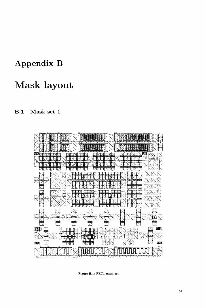
Appendix B
Mask layout
B.l Mask set 1
Figure B .l : FETl mask set
67

B . Mask layout
B.2 Mask set 2
MIS Diodes
Hall Bars -,., ... =-···--Figure B .2: FET2 mask set
68
Appendix C
Presented posters and published artiele
In this appendix, two posters are depicted. The first poster All-oxide transistors was presented at the National Solid State day at the Eindhoven University of Technology (8 may 1996). The second poster A compact model of ferroelectric field-effect transistors was presented at the F.O.M. days in Veldhoven (18 december 1997). An artiele Depletion-type thin-film transistors with a ferroelectric insuiator is published in Applied Physics Letters [22]. As the artiele is nat available at the moment of printing this report , an abstract is given below.
Depletion-type thin-film transistors with a ferroelectric insuiator
M.W.J. Prins, S.E. Zinnemers, J.F.M. Cillessen, and J.B . Giesbers
We present a study of electrical characteristics of ferroelectric field-effect transistors made of PbZr0.2Tio.sÛ3 and Sn02:Sb thin films. Due to properly chosen semiconductor parameters, the transistor channel can be totally depleted by the ferroelectric charge displacement. The observed remnant onjoff ratio of the channel current amounts to 7 x 10³. Pulse response measurements give information on data retention, device speed, and the occurrence of charge injection. The results lead to important design considerations for ferroelectric transistors.
69
C. Presented posters and publisbed artiele
70

ALL-OXIDE TRANSISTORS
S.E. Zino1111n °), B.LM. He•drikl .. -). J.f .M. Cill-en, Mil M.W.J. Pria
Philips Racan:h Laboratoria, Eindhovon, Prof. Holstlaan 4, 5656 AA Eindhoven, The Netherlancls ") Department ofSerniamduaor PhYJia. Eindhoven Univenity ofTechnolosr. The Netherlancls
"") Faculty of AppUed PhYJia. UllÎv<nity ofTwauc, The Netherlsncls
Introduetion
New functions can he implementeel in a ttansÏJtor by wing apecial matcrials in the dcsip. In thU poster we prescru a novd thin~film fidd-dfect tranàator with non--conventional oxidic conatitucrna: • Thc: inNlator c:on.&i.ta of a ferrodectric material, &ivina; Ne co a memory behavior. • The clwtnd a>ftiÎIU of SnO,:Sb, a
Th in-film transistor
!zsonm
Metenals
• The oulmrau: is a poUohed Sr1i0s (100) ainglecrysul. • The pre dearode a>ftJÎIU of an epituial SrRuOs film. • The inlulator is a>mpooed of an epicuial krrodecuic PbZro.2 T10.aOs la)'<f.
Previow nudia ohow an eudlent krrodecuic bebaviow for the a>rnbination of theae pavnkire-type matcrials On a capacitor).
• The tcmiconductinJ clwtnd <OI1IÎIU of an Sb doped Sn02 film. SnO,:Sb is a ...U lmown uarupom>t a>nductiv. ...ïde. ......._, for the fint time we apply SnO,:Sb for ia tcmiconductiw propertics in a ttaniÎJtOr. Ow films ohow a fine poined ltiUCtUfe (sninaizc 30-60 am). Foc SnO, fibm with a Sb doping a>ncentn.tion I'UIIin& between J017 and Jo» ="· Hall meuuranena show n-type a>nduaion and carrier mobilitics upto JO an2No.
Transistor preparetion
Thc thin films are grown by pulsed laser depoàtion. F'tm a a>nductinJ SrRuOs lay<r is depooiteel on SrTi03 and pte dearocla are mucrured by reaaiv< ion euiJin&. Thercsfi<r, the PhZr, .. r,._,o3 and the SnO,:Sb films are grown. Tbe clwtnd;, delined by ltfiiClUfÎill the SnO,:Sb.
Pulsed laser depoàtion: An intense pulaed laser bearn eaplooi.dy evaporata an amount of- matctiaL Specia of the induced eapancling plaana are depooired on the beored tubotnte. This way a JtOic:hiometric: tranlfer of - DW<rial ODIO me oubotn.a: is ocbieved.
Memory statas
n-typechenMI t.rr .. l•ctric polarization
helter
substr.t1
film
t OVIparontlplltmll
...... pul11d ln1r lt111n
-/N>NNI,HNI..-==
;t: Tbe rcsnnant dcctrical polarization of the ferrodectric inaulanu awa a displacement of the dwJe carriea in the oemicoDduanr: a,. • roEt, + P'" with a,. the efw&e denoity in the ocmia>nduanr, Ei, the dcctrical 6dd in the krrodecuic la)'<f and P" the ferrodectric polariaation.
Charge displacement Transfer characteristic
é:~ ~~~
-1-4-20241 VoM
1r·~ ... ~ .... ~~~~.~~2~.--.~ VoM
The dearic::ol efw&e per unit pt< ara dUplaad in the ferrodectric inoulator (QG} 11 a function of the pte .aluge (V c). The di.plaad efw&e is meuured with an enemal capacitor C (see inKt).
Ttanafer characterisric Oo venw Vc). The IOIU<e is ar zero pou:ntial and Vo-().1 V. Tbe pa:lealase cunent (lc<0.5 nA) dimubo the ttaNfer c:haracteristic bdow -3V.
Ttanafer characterisria for different ttaniÏJton. The h}'lt<rcsis bebaviour is due to the krrodcaric: polariution.
JI][I][Z[][I.][l] ~M ~M ~M ~M ~M
A
A • c D E
Ro !Ol 2.4><11f 2.Bx11f 2.6x11f 2x10⁵ 4x1o' Semiconductortblckneu (nm) 12 10 10 5 10 Sb doping concentrotion (cm.., 4><1011 4><1011 4x10¹¹ 4x1g20 4x10¹¹
lnaulotortbicknoaa (rvn) 250 250 250 225 350 -----------·---------~·-·--··-··----·~·········-·····-·--··-··· ·- ·-···
Relaxelion maasuremanis
Tune nolution of the drain current. with Vc..O V and Vo-().J V. Ar. tirn..O a pa: >t>luge pulse is applied. with an arnpUnule of .6 V for the on-ccate and ~ V for the offnate (ttaniÎJtOr C).
Pulse maasuremanis
~::(] ..... •r
Otf•ltlt.
•r,., la' ,,. lo' la'
tim•C•J
A minimum pubc width and hc:igltt is rcquired to switch thc: polariution (transistor B). ID"w ---~ 1r .._ __ ..
1r1r 1.-' 1r 1r ,...._1•1
Charge injection
Clw&< injeaion into the inaulanu oa:un for larp: pulx beipL This mluccs the dearic di.placemenL Charse injection rnay he a>mpared with dw&< - in • &o.tinc pte device (ttaniÎJtOr B).
Summary and conclusions
3: ,,~
-"
ur' D
7.0
1.1
l 1.1
-" 1.2
1.1
0.0
,...,.,r, I 2 3 4
puls• helght M
--M u .. \ I u - .......... .. _ -- -I \ ~· ....
..... 100 1000
timeCal
We demomtmed the opendoG offidd.dl<ct ttaniÎJtOa made of optically traiUpOfCDt osidic thin rum.. Tbe tnniÏIIna eabibit • -r function due to the ..... of • krrodecuic inoulator. Ow opàmiae
PH U. IPS

C. Presented posters and published artiele
72

A compact model of ferroelectric field-effect transistors
D.B.A. Rep•, S.E. ZlnnemersM and H.W.J. Prins
Phlllpo Roo.rch 1..1borau>ria. f'loo(, Hobdun 4. 5656 M Elnclhc>Ywl. The Nethwtands • Doponment of Appllod Phy>la. U.-aty of Gronlnpn. The Ne<hwtands
• 0oponment of Appllod Phy>la. a..- Unhwslty of Tochnolocy.The-
Introduetion
A dlln-61m field-effect aansistor witb a fcnoclcaric i..W.cor hu been d...Jopccl 1'IW device ;, oimiW co a JUDdanl field-effect aan&istor, only the oxide hu been r.plaad witb fcnoclcaric nwaial, cnabllnc tbc: tranJÏJtor co be """' u --~ memory clcvia. Mocldinc can ....., co pia mon: inJi&br into tbc: opcration of tbe clcvia. Therd'oro a compact mocld hu been deYdopcel to clacribe the fcnocl<Ctric .. ...n .. the (polyayJW!ine) Jemiconduain& .. ,....
Ferroelectrlc transistor
................
Modeling the ferroelectrlc layer
-- . .. --M Pn:viowly propooed mocld. of the fatodcaric ..,... ... nor oppropnare for a compact dacription. 5ome on: too
matbcmaác:al for uatmca.t in a dmce aimulation. pacb&o. ochcn on: far fiom bual on tbc: phyáal ptvpenia of fcnoclcaric laj>aa. On the buil of • oompact clacrip<ion of fcnoclcaric dwge dioplaceraen~ we propooe a model tbu co..UU of only a few dcaroaic: oomponen.., namdy n:aioton ("""17' cliaipuioa) and apacicort (clwJe -...>.
,...,..._,..... ..... ...,_.._ ..
Hodeling the semiconductor layer
land..fMndlns
Thc c:huJc that il induc.cd in a unit area ICIIÛconcluctina layu of tbiclmca r u condared witb tbc: band-bencline ~) of tbe conduction band-cd&e-~) u ciacribed u a lUnaion of dwJe dallity pCor) by Poiaon'• equarion V1
• •i&, .
Poillon'• equation can bc IDMd. uAna an dcctronie equinlcn.t c:irc:uit:
""
J.mi,J 6J•,.,..,...,.
re.~-'. ---iir'---lrt--------t_~ Tc.. Je..· T~ ____ __ ____Jc..a J;: __ ,
Cp,i : Qp,; • -ei /(E) D(E-41;) dE+ Qo (61finsof-l
D(E) : dallity of-I (E) : Fami-Dinc dimibutioa lUnaion Qs, : co=tbuQ,.I·Ofor~-o
Tranoport
lf,.. aaume a coOJUDt mobility for tbc: dccuona in the oonductioa bond. ,.. h... for tbc: .......,._ drain oonduaiYity:
u(x) • e ·Jl· i/(E) D(E-41(x)) dE •V<>
F....n,. the ""--<X>Dd......,.. u modeled by aa anay of n:aioton: , G". I u (x) dx
0
Vso
MI~]· ~
Experiment
F.,..,.lectric behavlour
v,M
s.,.,Jcontluctor propertiet
.... ...... J>,,..
....
11
From aaalyaU of the data and oimulatioru, it follow. dw:
Simulation
... . v,M
"'"'""'
• The h)'ltOftiÛ of the tranJÏJtor u due 10 the fcnoclecuic dwJe dioplacement.
• The mndulatioa of the channd oonduaance Ïl mainly ca""" by aernkanductor deplaion.
• The dallity ofJtara inaide tbe haadpp D1 (E);, oorutaat and approximatdy IO" crn-•.v-•. i rhe correct rance fora m.icro-polyayatne ICIIÜconduaor.
• The fidd-Gf.a mobility u about I cm> IVo, oimiW to tbe rneasun:d Hall-dl'ect mobility.
• The Jemiconduaor tbicknca dl'.ctM: for aarupon ;, lca tbaa the nomina! thickaeu. ThU ca be due 10 the paaular""""""' of the 61m or due 10 channd depletion aear tbc: cappinc layu.
Interface propertlu
... ~ ....
.....
The aperimeaal cuna ahow h)'ltOftiÛ behmour due co dwJe injeaioa. For tbc: inner loop la dwJe injeaion ocx:un. Cfwae injeaioa Ïl mndded by a n:aiotor and a apac:itor at tbc: fatodec:uK xmicooduaor intcr&ce.
Summary and conclusions We demorutrated tbu a fcnoclcaric fidd-effect lnDIÎitor can be ciacribed with a compact modi coaaioáac of oaly apac:i""' and n:aioton. The mocld ciacribeo tbc: fcnoclcaric dwp dioplaccmen1 dq>lcoioA of tbc: Jemiconduaor clwuod aad clwJe injeaion inco tbc: in...C.... Compariacm wid D'UliÏent esperimeaa (device apoed. rdaxaáon of tbc: fcnoclcaric and tbc: injecred dwp) ohou1d .U... for funber mocld ilnpnoftm<oa.
Adcnowleclpnena The outbon an: iadebad 10 J.F.M. cm-.. J.B. Gieaben and H.A. van ~!och for oomple pr<pamioa.
PH I UPS


![FERROELECTRIC RAM [FRAM]](https://img.dokumen.tips/doc/110x75/56816799550346895ddcd567/ferroelectric-ram-fram.jpg)


![Sangeetha [Ferroelectric Memory]](https://img.dokumen.tips/doc/110x75/55cf8f91550346703b9d9665/sangeetha-ferroelectric-memory.jpg)
