Embed Size (px)
Citation preview

ECC v2.0
LogiCORE IP Product Guide
Vivado Design Suite
PG092 June 7, 2017

ECC v2.0 www.xilinx.com 2PG092 June 7, 2017
Table of ContentsIP Facts
Chapter 1: OverviewFeature Summary. . . . . . . . . . . . . . . . . . . . . . . . . . . . . . . . . . . . . . . . . . . . . . . . . . . . . . . . . . . . . . . . . . 5Applications . . . . . . . . . . . . . . . . . . . . . . . . . . . . . . . . . . . . . . . . . . . . . . . . . . . . . . . . . . . . . . . . . . . . . . 8Licensing and Ordering Information . . . . . . . . . . . . . . . . . . . . . . . . . . . . . . . . . . . . . . . . . . . . . . . . . . . 9
Chapter 2: Product SpecificationPerformance. . . . . . . . . . . . . . . . . . . . . . . . . . . . . . . . . . . . . . . . . . . . . . . . . . . . . . . . . . . . . . . . . . . . . 10Resource Utilization. . . . . . . . . . . . . . . . . . . . . . . . . . . . . . . . . . . . . . . . . . . . . . . . . . . . . . . . . . . . . . . 12Port Descriptions . . . . . . . . . . . . . . . . . . . . . . . . . . . . . . . . . . . . . . . . . . . . . . . . . . . . . . . . . . . . . . . . . 13
Chapter 3: Designing with the CoreGeneral Design Guidelines . . . . . . . . . . . . . . . . . . . . . . . . . . . . . . . . . . . . . . . . . . . . . . . . . . . . . . . . . 16Clocking. . . . . . . . . . . . . . . . . . . . . . . . . . . . . . . . . . . . . . . . . . . . . . . . . . . . . . . . . . . . . . . . . . . . . . . . . 16Resets . . . . . . . . . . . . . . . . . . . . . . . . . . . . . . . . . . . . . . . . . . . . . . . . . . . . . . . . . . . . . . . . . . . . . . . . . . 16Latency . . . . . . . . . . . . . . . . . . . . . . . . . . . . . . . . . . . . . . . . . . . . . . . . . . . . . . . . . . . . . . . . . . . . . . . . . 17
Chapter 4: Design Flow StepsCustomizing and Generating the Core . . . . . . . . . . . . . . . . . . . . . . . . . . . . . . . . . . . . . . . . . . . . . . . . 19Constraining the Core . . . . . . . . . . . . . . . . . . . . . . . . . . . . . . . . . . . . . . . . . . . . . . . . . . . . . . . . . . . . . 21Simulation . . . . . . . . . . . . . . . . . . . . . . . . . . . . . . . . . . . . . . . . . . . . . . . . . . . . . . . . . . . . . . . . . . . . . . 22Synthesis and Implementation . . . . . . . . . . . . . . . . . . . . . . . . . . . . . . . . . . . . . . . . . . . . . . . . . . . . . . 22
Chapter 5: Example Design
Chapter 6: Test Bench
Appendix A: Verification, Compliance, and InteroperabilitySimulation . . . . . . . . . . . . . . . . . . . . . . . . . . . . . . . . . . . . . . . . . . . . . . . . . . . . . . . . . . . . . . . . . . . . . . 26Hardware Testing. . . . . . . . . . . . . . . . . . . . . . . . . . . . . . . . . . . . . . . . . . . . . . . . . . . . . . . . . . . . . . . . . 26
Send Feedback
ECC v2.0 www.xilinx.com 3PG092 June 7, 2017
Appendix B: Migrating and UpgradingMigrating to the Vivado Design Suite. . . . . . . . . . . . . . . . . . . . . . . . . . . . . . . . . . . . . . . . . . . . . . . . . 27Upgrading in the Vivado Design Suite . . . . . . . . . . . . . . . . . . . . . . . . . . . . . . . . . . . . . . . . . . . . . . . . 27
Appendix C: DebuggingFinding Help on Xilinx.com . . . . . . . . . . . . . . . . . . . . . . . . . . . . . . . . . . . . . . . . . . . . . . . . . . . . . . . . . 28Debug Tools . . . . . . . . . . . . . . . . . . . . . . . . . . . . . . . . . . . . . . . . . . . . . . . . . . . . . . . . . . . . . . . . . . . . . 29Hardware Debug . . . . . . . . . . . . . . . . . . . . . . . . . . . . . . . . . . . . . . . . . . . . . . . . . . . . . . . . . . . . . . . . . 29
Appendix D: Additional Resources and Legal NoticesXilinx Resources . . . . . . . . . . . . . . . . . . . . . . . . . . . . . . . . . . . . . . . . . . . . . . . . . . . . . . . . . . . . . . . . . . 31References . . . . . . . . . . . . . . . . . . . . . . . . . . . . . . . . . . . . . . . . . . . . . . . . . . . . . . . . . . . . . . . . . . . . . . 31Revision History . . . . . . . . . . . . . . . . . . . . . . . . . . . . . . . . . . . . . . . . . . . . . . . . . . . . . . . . . . . . . . . . . . 32Please Read: Important Legal Notices . . . . . . . . . . . . . . . . . . . . . . . . . . . . . . . . . . . . . . . . . . . . . . . . 32
Send Feedback

ECC v2.0 www.xilinx.com 4PG092 June 7, 2017 Product Specification
IntroductionThe Xilinx® LogiCORE IP Error Correction Code (ECC) core is ideal for robust data transmission with error correction and checking capabilities. The adaptable core supports Hamming and Hsiao algorithms for Single Error Correction and Double Error Detection (SEC-DED) error correction codes (ECC). The ECC core supports data widths between 4 and 128 bits and can be used with internal and external memories and with high speed Multi-Gigabit transceivers.
Features• Supports Single Bit Error correction and
double bit error detection functions
• Supports hamming algorithm for 4 to 64 data widths
• Supports Hsiao algorithm for 4 to 128 data widths
• Supports encode only, decode only and encode/decode modes
• Supports clock enable and synchronous active high reset
• Provides option to add input/output registering stages
• Provides optional internal pipelining stage for high frequency operations
• Supports dynamically enabling or disabling error correction function
• Provides Single Bit Error corrected and two bit error detected status outputs
IP Facts
LogiCORE IP Facts Table
Core Specifics
Supported Device Family(1)
UltraScale+™ Families,UltraScale™ Architecture, Virtex®-7,
Kintex®-7, Artix®-7
Supported User Interfaces Native
Resources See Table 2-3 and Table 2-4.
Provided with CoreDesign Files Encrypted RTL
Example Design Verilog
Test Bench Verilog
Constraints File XDC
Simulation Model Not Provided
Supported S/W Driver N/A
Tested Design Flows(2)
Design Entry Vivado Design Suite
Simulation For supported simulators, see theXilinx Design Tools: Release Notes Guide.
Synthesis Vivado Synthesis
SupportProvided by Xilinx at the Xilinx Support web page
Notes: 1. For a complete list of supported devices, see the Vivado IP
catalog .2. For the supported versions of the tools, see the
Xilinx Design Tools: Release Notes Guide.
Send Feedback

ECC v2.0 www.xilinx.com 5PG092 June 7, 2017
Chapter 1
OverviewSingle Error Correction and Double Error Detection (SEC-DED) error correction codes (ECC) are used to increase reliability against soft errors from random noise. As technology has scaled, the decreasing supply voltages and increasing interface speeds has resulted in reduced noise margins. This margin reduction increases the probability of soft errors introduced in both on-chip and off-chip FPGA components. For FPGA internal memory and external memories, error correction codes are needed to reduce radiation induced soft errors or single event upsets (SEU). For maintaining signal integrity, high-speed off-chip interfaces such as multi-gigabit transceivers also require increased protection against bit errors introduced due to the clock jitter or random noise. The ECC core increases system reliability under these random error conditions by detecting and correcting all single-bit errors. In addition, it detects double-bit errors in the data.
Feature SummaryThis section summarizes the functionality of the all three ECC core operations: encoder, decoder, encoder/decoder.
ECC Encoder OperationThe ECC encoder operation calculates check (or protection) bits for the input data. For each 4 to 128 bits of data input, it generates between 4 and 9 check bits. These bits are used during each ECC decoder operation to correct any single-bit errors, or to detect any double-bit errors. The data along with the calculated check bits are provided as an output of ECC encoder function, as shown in Figure 1-1. The data and check bits output of the ECC encoder is called an ECC codeword. For more details on the number of check bits required for the configured data width, see Vivado Integrated Design Environment in Chapter 4.
Send Feedback

ECC v2.0 www.xilinx.com 6PG092 June 7, 2017
Chapter 1: Overview
ECC Decoder OperationThe ECC decoder operation generates error correction syndrome bits for the input data and check bits. These syndrome bits are used to correct any single-bit errors, or to detect (but not correct) any double-bit errors in the input data. The single bit error corrected data, along with the ecc_sbit_err status or the uncorrected data with ecc_dbit_err status, are provided as an output of the ECC decoder function, as shown in Figure 1-2. If no errors are detected, input data is forwarded at the output, and both ecc_sbit_err and ecc_dbit_err status outputs are kept de-asserted.
The ECC decoder operations can also be bypassed by asserting the ecc_correct_n input. When the operations are bypassed, the input data is forwarded at the output, and both ecc_sbit_err and ecc_dbit_err status outputs are kept deasserted. The ECC bypass function can be applied when error protection/correction is not required for portions of data or payload provided to the ECC core.
X-Ref Target - Figure 1-1
Figure 1-1: ECC Encoder Block Diagram
X-Ref Target - Figure 1-2
Figure 1-2: ECC Decoder Block Diagram
Send Feedback

ECC v2.0 www.xilinx.com 7PG092 June 7, 2017
Chapter 1: Overview
ECC Encoder/Decoder OperationThe ECC encoder/decoder combines both encoder and decoder operations in a single module and is most suited for applications requiring either encoding or decoding but not both at the same time. The ECC encoder/decoder function provides an additional ecc_encode input. When this input is asserted High, ECC encoder operations are performed on the input data. When ecc_encode input is de-asserted, ECC decoder operations are performed on input codeword (data and check bits). When ecc_correct_n input is asserted High during ECC decoder operation, the decoding operation is bypassed and input data is forwarded at the output with error status outputs kept deasserted.
The ECC encoder/decoder function provides an optimized solution for Single Port Memory operations or for extending ECC function over byte enabled data with an external read-modify-write operation.
ECC Clock Enable and Registering OptionsThe ECC core supports multiple registering options. These options include input registering, output registering and an optional internal pipeline registering stage. Each registering stage can be independently enabled. The internal pipeline registering stage breaks the computation logic into two parts and can be used for higher data widths for frequency optimization. In addition, the clock enable can be used to save power. When one or more registering stages are enabled and when clock enable is used, the ECC core pipelines the data with respect to the clock enable.
X-Ref Target - Figure 1-3
Figure 1-3: ECC Encoder/Decoder Block Diagram
Send Feedback

ECC v2.0 www.xilinx.com 8PG092 June 7, 2017
Chapter 1: Overview
ApplicationsFigure 1-4 shows an example of the ECC Encoder and ECC Decoder use case. The ECC Encoder and ECC Decoder functions are used along with Internal Memories for single bit error correction function. The error correction function here increases reliability against radiation induced soft errors or Single Event upsets [SEU].
In Figure 1-5, ECC Encoder/Decoder function is used with the off-chip DDR memory. The write operations to the memory are performed using data byte enables or data strobes. Because ECC functions inherently do not support byte enables, to perform data writes with byte enables, a read-modify-write operation is used.
For DDR memory writes, first a read is performed to the memory. The codeword received from DDR memory is checked for single bit errors and then the corrected data is provided to read-modify-write operation. The output of read-modify-write operation is again provided to ECC core to generate the write codeword to the DDR Memory. For DDR memory
X-Ref Target - Figure 1-4
Figure 1-4: ECC Encoder and ECC Decoder Application Example
X-Ref Target - Figure 1-5
Figure 1-5: ECC Encoder/Decoder Application Example
DIMMECC Encoder/Decoder
Memory Controller
ecc_encode Address
Control
Data + CheckBits
Strobe
Read-Modify-Write
Engine
Data + Checkbits /Data + Error Status
DRAM Read Data + Check Bits
Read Data + Error Status
Write DataWrite Data
Data_Valid
RMW_Valid
Write Strobes
Read Valid / Write Valid / Address
Send Feedback

ECC v2.0 www.xilinx.com 9PG092 June 7, 2017
Chapter 1: Overview
reads, the codeword read from DDR Memory is checked for single bit errors by the ECC function. The corrected data along with error status is then provided at the user interface. A single instance of ECC encoder/decoder function is used here for both reads from the DDR memory to perform Read-Modify-Write to the DDR memory.
Note: The ECC functions supported are suited for applications requiring random bit error conditions and are not suited for applications requiring burst error detection or correction. For more than 2-bits in error, the supported ECC function does not guarantee a robust error detection operation and may even result in an incorrect single bit error correction operation.
Licensing and Ordering InformationThis Xilinx LogiCORE IP module is provided at no additional cost with the Xilinx Vivado Design Suite under the terms of the Xilinx End User License. Information about this and other Xilinx LogiCORE IP modules is available at the Xilinx Intellectual Property page. For information about pricing and availability of other Xilinx LogiCORE IP modules and tools, contact your local Xilinx sales representative.
Send Feedback
ECC v2.0 www.xilinx.com 10PG092 June 7, 2017
Chapter 2
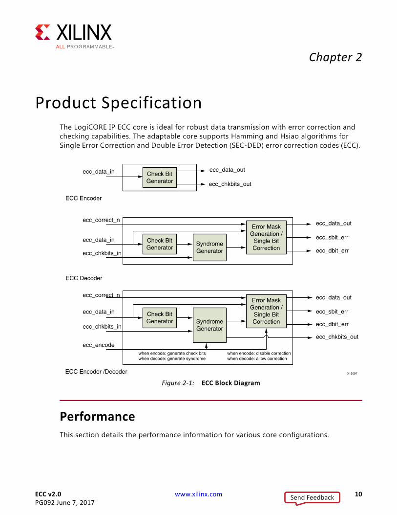
Product SpecificationThe LogiCORE IP ECC core is ideal for robust data transmission with error correction and checking capabilities. The adaptable core supports Hamming and Hsiao algorithms for Single Error Correction and Double Error Detection (SEC-DED) error correction codes (ECC).
PerformanceThis section details the performance information for various core configurations.
X-Ref Target - Figure 2-1
Figure 2-1: ECC Block Diagram
Send Feedback
ECC v2.0 www.xilinx.com 11PG092 June 7, 2017
Chapter 2: Product Specification
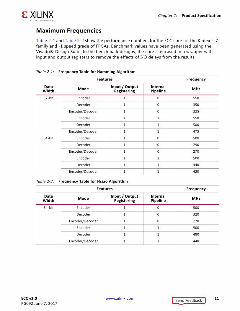
Maximum FrequenciesTable 2-1 and Table 2-2 show the performance numbers for the ECC core for the Kintex™-7 family and -1 speed grade of FPGAs. Benchmark values have been generated using the Vivado® Design Suite. In the benchmark designs, the core is encased in a wrapper with input and output registers to remove the effects of I/O delays from the results.
Table 2-1: Frequency Table for Hamming Algorithm
Features Frequency
Data Width Mode Input / Output
RegisteringInternal Pipeline MHz
32-bit Encoder 1 0 550
Decoder 1 0 350
Encoder/Decoder 1 0 325
Encoder 1 1 550
Decoder 1 1 500
Encoder/Decoder 1 1 475
64-bit Encoder 1 0 500
Decoder 1 0 290
Encoder/Decoder 1 0 270
Encoder 1 1 500
Decoder 1 1 440
Encoder/Decoder 1 1 420
Table 2-2: Frequency Table for Hsiao Algorithm
Features Frequency
Data Width Mode Input / Output
RegisteringInternal Pipeline MHz
64-bit Encoder 1 0 500
Decoder 1 0 320
Encoder/Decoder 1 0 270
Encoder 1 1 500
Decoder 1 1 480
Encoder/Decoder 1 1 440
Send Feedback

ECC v2.0 www.xilinx.com 12PG092 June 7, 2017
Chapter 2: Product Specification
LatencyThe latency of the signals of the ECC core varies for different Configurations. See Latency in Chapter 3 for more details.
Resource UtilizationTable 2-3 and Table 2-4 show the resource utilization numbers for the ECC core for the Kintex™-7 family and -1 speed grade of FPGAs. Benchmark values have been generated using the Xilinx Vivado Design Suite.
128-bit Encoder 1 0 425
Decoder 1 0 250
Encoder/Decoder 1 0 210
Encoder 1 1 425
Decoder 1 1 400
Encoder/Decoder 1 1 360
Table 2-3: Resource Utilization for Hamming Algorithm
Features Resources
Data Width Mode Input
RegisteringOutput
RegisteringInternal Pipeline Slices LUTs FFs
32- bit Encoder 0 0 0 9 28 0
Decoder 0 0 0 24 83 0
Encoder/Decoder 0 0 0 30 101 0
Encoder 1 0 0 14 28 32
Decoder 0 1 1 28 87 82
Encoder/Decoder 1 1 1 37 100 131
64-bit Encoder 0 0 0 18 53 0
Decoder 0 0 0 43 155 0
Encoder/Decoder 0 0 0 49 169 0
Encoder 1 0 0 34 53 64
Decoder 0 1 1 54 164 148
Encoder/Decoder 1 1 1 83 180 231
Table 2-2: Frequency Table for Hsiao Algorithm (Cont’d)
Features Frequency
Data Width Mode Input / Output
RegisteringInternal Pipeline MHz
Send Feedback

ECC v2.0 www.xilinx.com 13PG092 June 7, 2017
Chapter 2: Product Specification
Port DescriptionsTable 2-5 details the ECC core global signals.
Table 2-6 details the ECC core signals.
Table 2-4: Resource Utilization for Hsiao Algorithm
Features Resources
Data Width Mode Input
RegisteringOutput
RegisteringInternal Pipeline Slices LUTs FFs
64- bit Encoder 0 0 0 14 47 0
Decoder 0 0 0 47 164 0
Encoder/Decoder 0 0 0 53 184 0
Encoder 1 0 0 33 47 64
Decoder 0 1 1 65 171 139
Encoder/Decoder 1 1 1 83 172 223
128-bit Encoder 0 0 0 29 100 0
Decoder 0 0 0 88 299 0
Encoder/Decoder 0 0 0 93 313 0
Encoder 1 0 0 71 102 128
Decoder 0 1 1 119 292 268
Encoder/Decoder 1 1 1 226 293 416
Table 2-5: ECC Core Global Signals
Name Direction Description
ecc_clk Input ECC Clock: Applicable when one or more registering stages are enabled for the core. ECC core operations are synchronous to ecc_clk signal
ecc_clken Input ECC Clock Enable: Applicable when one or more registering stages are enabled for the core. When ecc_clken is used, ECC core operations are synchronous to ecc_clk clock and ecc_clken.
ecc_reset Input ECC Reset: Applicable when one or more registering stages are enabled for the core. This signal is synchronous and active-High.
Send Feedback

ECC v2.0 www.xilinx.com 14PG092 June 7, 2017
Chapter 2: Product Specification
Table 2-6: ECC Core Signals
Name Direction Description
ecc_data_in[C_DATA_WIDTH -1:0] Input Data Input: For generating check bits or protection bits. The valid range for input data width is from 4 to 128 bits
ecc_data_out[C_DATA_WIDTH -1:0] Output Data Output: The valid range for output data width is from 4 to 128 bits.• Encoder Mode: Data Output with the
associated check bits after encoding operation. • Decoder Mode: Data Output after decoding
operations, corrected for any single bit errors• Encoder/Decoder Mode: When ecc_encode is
asserted High, provides Data Output with the associated check bits. When ecc_encode is de-asserted, provides Data Output, corrected for any single bit errors
ecc_chkbits_in[C_CHK_BIT_WIDTH -1:0] Input Input Check Bits: Applicable for decoder and encoder/decoder modes of operation. The valid range for check bit width is from 4 to 9 bits. See Table 4-1 for minimum number of check bits required for the configured data width.• Decoder Mode: Input check bits for error
analysis over the associated data• Encoder/Decoder Mode: Ignored when
ecc_encode is asserted High. When ecc_encode is de-asserted, input check bits for error analysis over the associated data
ecc_chkbits_out[C_CHK_BIT_WIDTH-1:0] Output Output Check Bits/Syndrome (Encoder and Encoder/Decoder modes only): The valid range for check bit width is from 4 to 9 bits. See Table 4-1 for minimum number of check bits required for the configured data width.• Encoder Mode: Provides calculated check bits. • Encoder/Decoder Mode: When ecc_encode is
asserted High, provides calculated check bits. When ecc_encode is de-asserted, provides calculated syndrome.
Send Feedback

ECC v2.0 www.xilinx.com 15PG092 June 7, 2017
Chapter 2: Product Specification
ecc_correct_n Input Disable Error Correction: Applicable for decoder and encoder/decoder mode of operation. When asserted High, suppresses single bit error correction in the data. • Decoder Mode: When asserted High, input data
is forwarded at the output, and both ecc_sbit_err and ecc_dbit_err status outputs are kept deasserted.
• Encoder/Decoder Mode: Ignored when ecc_encode is asserted High.
When ecc_encode is de-asserted and ecc_correct_n is asserted High, input data is forwarded at the output, and both ecc_sbit_err and ecc_dbit_err status outputs are kept de-asserted.
ecc_sbit_err Output Single-Bit Error: Applicable for decoder and encoder/decoder modes of operation. When asserted High, flags the presence of a single-bit error in data which has been auto-corrected during ECC decoder operations.
ecc_dbit_err Output Double-Bit Error: Applicable for decoder and encoder/decoder modes of operation. When asserted High, flags the presence of a double-bit error in data. Double-bit errors cannot be auto-corrected during ECC decoder operations.
ecc_encode Input Encoder Enable: Applicable for only encoder/decoder mode of operation. When asserted High, the core performs encoding operations. When ecc_encode is de-asserted, the core performs decoding and/or error correction operations.
Table 2-6: ECC Core Signals (Cont’d)
Name Direction Description
Send Feedback

ECC v2.0 www.xilinx.com 16PG092 June 7, 2017
Chapter 3
Designing with the CoreThis chapter includes guidelines and additional information to facilitate designing with the core.
General Design GuidelinesThe customizable ECC core provides multiple registering options to the user. You can set the frequency at which the core needs to operate. Based on the required frequency, select the appropriate pipeline or input/output registering option. Each registering stage will impact the latency of the core by one clock cycle.
The clock enable functionality can be used when one or more registering stages are enabled for the core. The clock enable function allows the core to perform operations only when both clock and clock enable are asserted High. Based on the synchronous elements gated by a common clock enable in the design, the ECC core can also be constrained with the clock enable period instead of applied clock period.
ClockingThe ECC core has a single clock (ecc_clk) input and is used only when one or more registering stages are enabled for the design.
ResetsThe ECC core supports an active-High synchronous reset (ecc_reset) input. The reset input is applicable only when one or more registering stages are enabled for the design.
Send Feedback

ECC v2.0 www.xilinx.com 17PG092 June 7, 2017
Chapter 3: Designing with the Core
LatencyThe ECC core supports Input Registering, Output Registering and Internal Pipeline Registering options. Each of these registering stages can be independently enabled during core generation. The clock cycle latency of the core equals the number of registering stages selected. There is no clock cycle latency when none of the registering stages are selected; in this case the core latency is determined by logical delay of the core. For more details on ECC core delays, see Maximum Frequencies in Chapter 2.
When Clock Enable is used with the registering stages, ECC core operations are synchronous to both ECC clock and ECC Clock Enable. In this case, clock cycle latency of the core equals the number registering stages only when both clock and clock enable are asserted High.
Figure 3-1 provides timing diagram for ECC Encoder function with a single stage of registering. With the clock-enable signal set to high, the calculated check bits and data appear here at the next rising edge of the clock. The clock enable feature when enabled allows to control when encoded data should appear on the output port.
Figure 3-2 provides timing diagram for ECC Decoder function with two stages of registering. The data corrected for any single bit error and status outputs here appears after two rising edges of the clock. The clock enable feature here is used to perform each ECC operation in two clock cycles.
X-Ref Target - Figure 3-1
Figure 3-1: ECC Encoder Single-Stage Registering
Core latency with 1-stage registering
ECC Encoding outputs Disable Encoding ECC Encoding outputs
Send Feedback

ECC v2.0 www.xilinx.com 18PG092 June 7, 2017
Chapter 3: Designing with the Core
Figure 3-3 provides timing diagram for ECC Encoder/Decoder function with three stages of registering. When ecc_encode input is asserted High, ECC Encoder operations are performed on the input data and the calculated check bits and data appear after three rising edges of the clock. When ecc_encode input is de-asserted ECC Decoder operations are performed on input data and check bits, the data corrected for any single bit error and status outputs appears here after three rising edge of the clock.
X-Ref Target - Figure 3-2
Figure 3-2: ECC Decoder Two-Stage Registering
X-Ref Target - Figure 3-3
Figure 3-3: ECC Encoder/Decoder Three-Stage Registering
Core latency with 2-stage registering
ECC Decoding outputs Disable Decoding
Core latency with 3-stage registering
ECC Encoding outputs Disable Decoding
ECC Decoding outputs
Send Feedback

ECC v2.0 www.xilinx.com 19PG092 June 7, 2017
Chapter 4
Design Flow StepsThis chapter describes customizing and generating the core, constraining the core, and the simulation, synthesis and implementation steps that are specific to this IP core. More detailed information about the standard Vivado® design flows and the IP integrator can be found in the following Vivado Design Suite user guides:
• Vivado Design Suite User Guide: Designing IP Subsystems using IP Integrator (UG994) [Ref 3]
• Vivado Design Suite User Guide: Designing with IP (UG896) [Ref 6]
• Vivado Design Suite User Guide: Getting Started (UG910) [Ref 9]
• Vivado Design Suite User Guide: Logic Simulation (UG900) [Ref 4]
Customizing and Generating the CoreThis section includes information about using Xilinx tools to customize and generate the core in the Vivado Design Suite environment.
Vivado Integrated Design EnvironmentYou can customize the IP for use in your design by specifying values for the various parameters associated with the IP core using the following steps:
1. Select the IP from the IP catalog.
2. Double-click the selected IP or select the Customize IP command from the toolbar or right-click menu .
For details, see the Vivado Design Suite User Guide: Designing with IP (UG896) [Ref 6] and the Vivado Design Suite User Guide: Getting Started (UG910) [Ref 9].
Note: Figures in this chapter are illustrations of the Vivado Integrated Design Environment (IDE). This layout might vary from the current version.
Figure 4-1 shows the Vivado IDE for the ECC core.
Send Feedback

ECC v2.0 www.xilinx.com 20PG092 June 7, 2017
Chapter 4: Design Flow Steps
• Algorithm Option: Selects Hamming or Hsiao algorithms for ECC operations. The algorithm selected must be the same for encoder and decoder cores for ECC encoding and subsequent decoding operations.
• ECC Mode: Selects Encoder, Decoder or Encoder/Decoder operations of the ECC core.
• Data Width: Configures the width of data in bits for ECC operations. The valid range for data width is 4 to 64 bits for Hamming and 4 to 128 bits for HSIAO algorithm.
Table 4-1 provides the minimum number of check bits required for the configured data width in bits.
• Enable Input Registering: When selected, the ECC core registers all of its inputs.
• Enable Pipeline Registering: When selected, the ECC core inserts an internal pipeline register stage to the core.
X-Ref Target - Figure 4-1
Figure 4-1: ECC in the Vivado IDE
Table 4-1: Minimum Check Bits Utilization
Data Width (Bits) Minimum Check Bits
4 4
5-11 5
12-26 6
27-57 7
58-64 8
65-128 9
Send Feedback

ECC v2.0 www.xilinx.com 21PG092 June 7, 2017
Chapter 4: Design Flow Steps
• Enable Output Registering: When selected, the ECC core registers all of its outputs.
Output GenerationFor details, see “Generating IP Output Products” in the Vivado Design Suite User Guide: Designing with IP (UG896) [Ref 6].
Constraining the CoreThis section contains information about constraining the core in the Vivado® Design Suite.
Required ConstraintsThe ECC core constraints can be applied from the top-level constraints file. Clock constraint can be applied when one or more registering stages are selected for the core. Max delay constraint can be applied in case none of the registering stages are selected for the core.
Device, Package, and Speed Grade SelectionsSee IP Facts for details about support devices.
Clock FrequenciesThere are no clock frequency constraints for this core.
Clock ManagementThere are no additional clock management constraints for this core.
Clock PlacementThere are no additional clock placement constraints for this core.
BankingThere are no banking constraints for this core.
Transceiver PlacementThere are no transceiver constraints for this core.
Send Feedback

ECC v2.0 www.xilinx.com 22PG092 June 7, 2017
Chapter 4: Design Flow Steps
I/O Standard and PlacementThere are no I/O constraints for this core.
SimulationFor details, see the Vivado Design Suite User Guide: Logic Simulation (UG900) [Ref 4].
Synthesis and ImplementationFor details about synthesis and implementation, see the Vivado Design Suite User Guide: Designing with IP (UG896) [Ref 6].
Send Feedback
ECC v2.0 www.xilinx.com 23PG092 June 7, 2017
Chapter 5
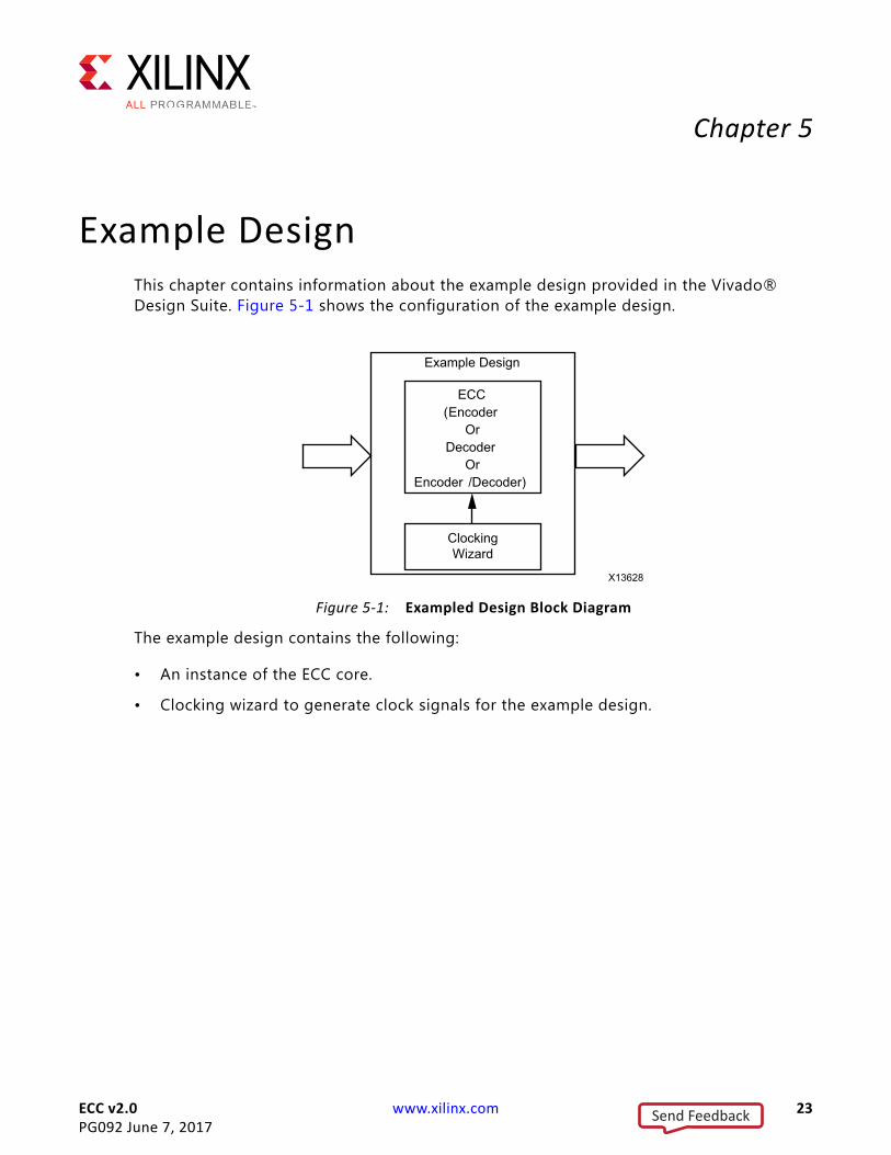
Example DesignThis chapter contains information about the example design provided in the Vivado® Design Suite. Figure 5-1 shows the configuration of the example design.
The example design contains the following:
• An instance of the ECC core.
• Clocking wizard to generate clock signals for the example design.
X-Ref Target - Figure 5-1
Figure 5-1: Exampled Design Block Diagram
ECC (Encoder
Or Decoder
OrEncoder /Decoder)
Example Design
X13628
ClockingWizard
Send Feedback
ECC v2.0 www.xilinx.com 24PG092 June 7, 2017
Chapter 6
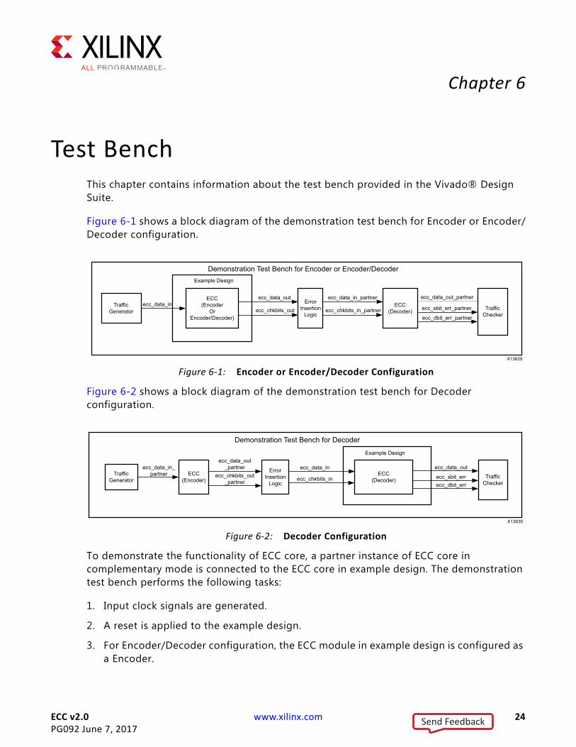
Test BenchThis chapter contains information about the test bench provided in the Vivado® Design Suite.
Figure 6-1 shows a block diagram of the demonstration test bench for Encoder or Encoder/Decoder configuration.
Figure 6-2 shows a block diagram of the demonstration test bench for Decoder configuration.
To demonstrate the functionality of ECC core, a partner instance of ECC core in complementary mode is connected to the ECC core in example design. The demonstration test bench performs the following tasks:
1. Input clock signals are generated.
2. A reset is applied to the example design.
3. For Encoder/Decoder configuration, the ECC module in example design is configured as a Encoder.
X-Ref Target - Figure 6-1
Figure 6-1: Encoder or Encoder/Decoder Configuration
X-Ref Target - Figure 6-2
Figure 6-2: Decoder Configuration
ECC (Encoder
OrEncoder/Decoder)
Example Design
Traffic Generator
ecc_data_in Error Insertion
Logic
ecc_data_out
ecc_chkbits_outECC
(Decoder)
ecc_data_in_partner
ecc_chkbits_in_partner
ecc_data_out_partner
ecc_sbit_err_partner
ecc_dbit_err_partner
Traffic Checker
Demonstration Test Bench for Encoder or Encoder/Decoder
X13629
ECC (Encoder)
Example Design
Traffic Generator
ecc_data_in_partner Error
Insertion Logic
ecc_data_out_partner
ecc_chkbits_out_partner
ECC (Decoder)
ecc_data_in
ecc_chkbits_in
ecc_data_out
ecc_sbit_errecc_dbit_err
Traffic Checker
Demonstration Test Bench for Decoder
X13630
Send Feedback

ECC v2.0 www.xilinx.com 25PG092 June 7, 2017
Chapter 6: Test Bench
4. Clock enable for the ECC core is generated, in cases where registering is involved.
5. ecc_corrent_n signal is de-asserted.
6. The traffic generator starts generating data for ten clock periods continuously.
7. The Error Insertion Logic inserts single- and double-bit errors alternatively in the encoded data.
8. The Traffic Checker checks the output data from the ECC Decoder. When a single-bit error or a double-bit error is not detected, the test bench errors out with ERROR : single/double bit error not detected in the console. When a single bit error is not corrected, the error message "ERROR : expected data mis-match = expected, actual" is issued at the console.
9. Ten transactions are showcased in the test bench. The test bench finishes with the message Test Completed Successfully.
Send Feedback

ECC v2.0 www.xilinx.com 26PG092 June 7, 2017
Appendix A
Verification, Compliance, and Interoperability
This appendix provides details about how this IP core was tested for compliance.
SimulationThe ECC core has been tested with Xilinx® Vivado™ Design Suite and Mentor Graphics Questa SIM simulator.
Hardware TestingThe ECC core has been validated at 200 MHz on KC705 board using Kintex-7 FPGA -2 speed grade device (325T). The core was configured for encoder, decoder, encoder/decoder modes across 4-128 data widths.
Send Feedback

ECC v2.0 www.xilinx.com 27PG092 June 7, 2017
Appendix B
Migrating and UpgradingThis appendix contains information about migrating a design from ISE® to the Vivado® Design Suite, and for upgrading to a more recent version of the IP core. For customers upgrading in the Vivado Design Suite, important details (where applicable) about any port changes and other impact to user logic are included.
Migrating to the Vivado Design SuiteFor information about migrating to the Vivado Design Suite, see the ISE to Vivado Design Suite Migration Guide (UG911) [Ref 7].
Upgrading in the Vivado Design SuiteThis section provides information about any changes to the user logic or port designations that take place when you upgrade to a more current version of this IP core in the Vivado Design Suite.
Parameter Changes There are no parameter changes.
Port ChangesThere are no port changes.
Send Feedback

ECC v2.0 www.xilinx.com 28PG092 June 7, 2017
Appendix C
DebuggingThis appendix includes details about resources available on the Xilinx Support website and debugging tools.
Finding Help on Xilinx.comTo help in the design and debug process when using the ECC, the Xilinx Support web page (Xilinx Support web page) contains key resources such as product documentation, release notes, answer records, information about known issues, and links for obtaining further product support.
DocumentationThis product guide is the main document associated with the ECC. This guide, along with documentation related to all products that aid in the design process, can be found on the Xilinx Support web page or by using the Xilinx Documentation Navigator.
Download the Xilinx Documentation Navigator from the Downloads page. For more information about this tool and the features available, open the online help after installation.
Answer RecordsAnswer Records include information about commonly encountered problems, helpful information on how to resolve these problems, and any known issues with a Xilinx product. Answer Records are created and maintained daily ensuring that users have access to the most accurate information available.
Answer Records for this core are listed below, and can be located by using the Search Support box on the main Xilinx support web page. To maximize your search results, use proper keywords such as
• Product name
• Tool message(s)
• Summary of the issue encountered
Send Feedback

ECC v2.0 www.xilinx.com 29PG092 June 7, 2017
Appendix C: Debugging
A filter search is available after results are returned to further target the results.
Technical SupportXilinx provides technical support in the Xilinx Support web page for this LogiCORE™ IP product when used as described in the product documentation. Xilinx cannot guarantee timing, functionality, or support if you do any of the following:
• Implement the solution in devices that are not defined in the documentation.
• Customize the solution beyond that allowed in the product documentation.
• Change any section of the design labeled DO NOT MODIFY.
To contact Xilinx Technical Support, navigate to the Xilinx Support web page.
Debug ToolsThere are many tools available to address ECC design issues. It is important to know which tools are useful for debugging various situations.
Vivado Design Suite Debug FeatureVivado lab tools insert logic analyzer and virtual I/O cores directly into your design. Vivado lab tools allow you to set trigger conditions to capture application and integrated block port signals in hardware. Captured signals can then be analyzed. This feature represents the functionality in the Vivado IDE that is used for logic debugging and validation of a design running in Xilinx FPGA devices in hardware.
The Vivado lab tools logic analyzer is used to interact with the logic debug LogiCORE IP cores, including:
• ILA 2.0 (and later versions)
• VIO 2.0 (and later versions)
See Vivado Design Suite User Guide: Programming and Debugging [Ref 8].
Hardware DebugHardware issues can range from link bring-up to problems seen after hours of testing. This section provides debug steps for common issues.
Send Feedback

ECC v2.0 www.xilinx.com 30PG092 June 7, 2017
Appendix C: Debugging
General ChecksEnsure that all the timing constraints for the core were properly incorporated from the example design and that all constraints were met during implementation.
• Does it work in post-place and route timing simulation? If problems are seen in hardware but not in timing simulation, this could indicate a PCB issue. Ensure that all clock sources are active and clean.
• If using MMCMs in the design, ensure that all MMCMs have obtained lock by monitoring the locked port.
• If your outputs go to 0, check your licensing.
Send Feedback

ECC v2.0 www.xilinx.com 31PG092 June 7, 2017
Appendix D
Additional Resources and Legal NoticesThis appendix contains additional resources for the ECC core.
Xilinx ResourcesFor support resources such as Answers, Documentation, Downloads, and Forums, see Xilinx Support.
ReferencesThese documents provide supplemental material useful with this product guide:
1. R. W. Hamming. 1950. "Error Detecting and Error Correcting Codes," Bell System Technical Journal.
2. M. Y. Hsiao. 1970. "A Class of Optimal Minimum Odd-weight-column SEC-DED Codes," IBM Journal of Research and Development.
3. Vivado Design Suite User Guide: Designing IP Subsystems using IP Integrator (UG994)
4. Vivado Design Suite User Guide: Logic Simulation (UG900)
5. Vivado Design Suite User Guide: Implementation (UG904)
6. Vivado Design Suite User Guide: Designing with IP (UG896)
7. ISE to Vivado Design Suite Migration Methodology Guide (UG911)
8. Vivado Design Suite User Guide: Programming and Debugging (UG908)
9. Vivado Design Suite User Guide: Getting Started (UG910)
Send Feedback

ECC v2.0 www.xilinx.com 32PG092 June 7, 2017
Appendix D: Additional Resources and Legal Notices
Revision HistoryThe following table shows the revision history for this document.
Please Read: Important Legal NoticesThe information disclosed to you hereunder (the "Materials") is provided solely for the selection and use of Xilinx products. To the maximum extent permitted by applicable law: (1) Materials are made available "AS IS" and with all faults, Xilinx hereby DISCLAIMS ALL WARRANTIES AND CONDITIONS, EXPRESS, IMPLIED, OR STATUTORY, INCLUDING BUT NOT LIMITED TO WARRANTIES OF MERCHANTABILITY, NON-INFRINGEMENT, OR FITNESS FOR ANY PARTICULAR PURPOSE; and (2) Xilinx shall not be liable (whether in contract or tort, including negligence, or under any other theory of liability) for any loss or damage of any kind or nature related to, arising under, or in connection with, the Materials (including your use of the Materials), including for any direct, indirect, special, incidental, or consequential loss or damage (including loss of data, profits, goodwill, or any type of loss or damage suffered as a result of any action brought by a third party) even if such damage or loss was reasonably foreseeable or Xilinx had been advised of the possibility of the same. Xilinx assumes no obligation to correct any errors contained in the Materials or to notify you of updates to the Materials or to product specifications. You may not reproduce, modify, distribute, or publicly display the Materials without prior written consent. Certain products are subject to the terms and conditions of Xilinx's limited warranty, please refer to Xilinx's Terms of Sale which can be viewed at https://www.xilinx.com/legal.htm#tos; IP cores may be subject to warranty and support terms contained in a license issued to you by Xilinx. Xilinx products are not designed or intended to be fail-safe or for use in any application requiring fail-safe performance; you assume sole risk and liability for use of Xilinx products in such critical applications, please refer to Xilinx's Terms of Sale which can be viewed at https://www.xilinx.com/legal.htm#tos.AUTOMOTIVE APPLICATIONS DISCLAIMERAUTOMOTIVE PRODUCTS (IDENTIFIED AS “XA” IN THE PART NUMBER) ARE NOT WARRANTED FOR USE IN THE DEPLOYMENT OF AIRBAGS OR FOR USE IN APPLICATIONS THAT AFFECT CONTROL OF A VEHICLE (“SAFETY APPLICATION”) UNLESS THERE IS A SAFETY CONCEPT OR REDUNDANCY FEATURE CONSISTENT WITH THE ISO 26262 AUTOMOTIVE SAFETY STANDARD (“SAFETY DESIGN”). CUSTOMER SHALL, PRIOR TO USING OR DISTRIBUTING ANY SYSTEMS THAT INCORPORATE PRODUCTS, THOROUGHLY TEST SUCH SYSTEMS FOR SAFETY PURPOSES. USE OF PRODUCTS IN A SAFETY APPLICATION WITHOUT A SAFETY DESIGN IS FULLY AT THE RISK OF CUSTOMER, SUBJECT ONLY TO APPLICABLE LAWS AND REGULATIONS GOVERNING LIMITATIONS ON PRODUCT LIABILITY.© Copyright 2012-2017 Xilinx, Inc. Xilinx, the Xilinx logo, Artix, ISE, Kintex, Spartan, Virtex, Vivado, Zynq, and other designated brands included herein are trademarks of Xilinx in the United States and other countries. All other trademarks are the property of their respective owners.
Date Version Revision
06/07/2017 2.0 Updated the Data Width for Minimum Check Bits of 8 and 9 in Minimum Check Bits Utilization Table (Table 4-1) in Chapter 4, Design Flow Steps.
04/05/2017 2.0 Updated the Minimum Check Bits Utilization Table (Table 4-1) in Chapter 4, Design Flow Steps.
11/18/2015 2.0 Added support for UltraScale+ devices.
04/02/2014 2.0 Added support for UltraScale™ architecture-based devices.
10/02/2013 2.0 Added Chapter 8, Example Design and Chapter 9, Test Bench.
03/20/2013 2.0 Updated core to v2.0.
10/16/2012 1.0 Initial Xilinx release.
Send Feedback