Embed Size (px)
Citation preview

LogiCORE IP Aurora 8B/10B v7.1
User Guide
UG766 October 19, 2011

Notice of Disclaimer The information disclosed to you hereunder (the “Materials”) is provided solely for the selection and use of Xilinx products. To the maximum extent permitted by applicable law: (1) Materials are made available "AS IS" and with all faults, Xilinx hereby DISCLAIMS ALL WARRANTIES AND CONDITIONS, EXPRESS, IMPLIED, OR STATUTORY, INCLUDING BUT NOT LIMITED TO WARRANTIES OF MERCHANTABILITY, NON-INFRINGEMENT, OR FITNESS FOR ANY PARTICULAR PURPOSE; and (2) Xilinx shall not be liable (whether in contract or tort, including negligence, or under any other theory of liability) for any loss or damage of any kind or nature related to, arising under, or in connection with, the Materials (including your use of the Materials), including for any direct, indirect, special, incidental, or consequential loss or damage (including loss of data, profits, goodwill, or any type of loss or damage suffered as a result of any action brought by a third party) even if such damage or loss was reasonably foreseeable or Xilinx had been advised of the possibility of the same. Xilinx assumes no obligation to correct any errors contained in the Materials or to notify you of updates to the Materials or to product specifications. You may not reproduce, modify, distribute, or publicly display the Materials without prior written consent. Certain products are subject to the terms and conditions of the Limited Warranties which can be viewed at http://www.xilinx.com/warranty.htm; IP cores may be subject to warranty and support terms contained in a license issued to you by Xilinx. Xilinx products are not designed or intended to be fail-safe or for use in any application requiring fail-safe performance; you assume sole risk and liability for use of Xilinx products in Critical Applications: http://www.xilinx.com/warranty.htm#critapps.
© Copyright 2010–2011 Xilinx, Inc. Xilinx, the Xilinx logo, Artix, ISE, Kintex, Spartan, Virtex, Zynq, and other designated brands included herein are trademarks of Xilinx in the United States and other countries. AMBA, AMBA Designer, ARM, ARM1176JZ-S, CoreSight, Cortex, and PrimeCell are trademarks of ARM in the EU and other countries. All other trademarks are the property of their respective owners.
Revision HistoryThe following table shows the revision history for this document.
Date Version Revision
09/21/10 1.0First release of the core with AXI interface support. The previous release of this document was UG353.
LogiCORE IP Aurora 8B/10B User Guide www.xilinx.com UG766 October 19, 2011

03/01/11 1.1
ISE 13.1 software release with v6.2 core. Removed references to Virtex-5 devices, including Appendix. Changed <component_name> to <component name> throughout. Updated signal names in waveforms to reflect AXI nomenclature. Updated GUI screen captures. Moved Supported Tools and System Requirements into Chapter 1 and removed Chapter 2, Installing and Licensing the Core, because a license is no longer required. Added <component name>.xise to Table 11-1, <component name>.v[hd] to Table 11-4, and implement_planahead.tcl to Table 11-9, simulate_isim.bat, simulate_isim.sh, and wave_isim.tcl to Table 11-11. In Table 11-11, changed the name of mti_wave.do to wave_mti.do. Added note on page 93 to Appendix D. Added step 9 to Case 2: Virtex-6 FPGA GTX Wrapper. Added step 11 to Case 3: Spartan-6 FPGA GTP Wrapper.
10/19/11 1.2
ISE 13.3 software release with v7.1 core. Added support for Virtex-7 and Kintex-7 FPGAs. Removed references to RX/TX Simplex operation. Removed Preface.
• Chapter 1: Added List of Acronyms.• Chapter 3: Changed valid range in Aurora Lanes, page 15. Updated Lane Width,
page 15. • Chapter 4: Updated Figure 4-8 and associated note. • Chapter 6: Added CPLLLOCKDETCLK_IN to Table 6-1. • Chapter 8: Added text about simulating simplex cores at the end of Simulating the
Example Design, page 75.• Added Chapter 10, Debugging the Aurora Core with ChipScope Pro Analyzer.• Chapter 11: Added Aurora core top-level module to Table 11-1. Changed name of
README file in Table 11-2. Added version information file to Table 11-3. Added NGC and script files to Table 11-9. Added Cadence IES simulator scripts to Table 11-11.
• Added Appendix A, Additional Resources. • Appendix D: Added Case 1: Virtex-7/Kintex-7 FPGA Wrapper Compatibility, page 94.
Removed step 9 from Case 2: Virtex-6 FPGA GTX Wrapper. Removed step 11 from Case 3: Spartan-6 FPGA GTP Wrapper.
• Appendix E: Moved and updated the Limitations section.
Date Version Revision
UG766 October 19, 2011 www.xilinx.com LogiCORE IP Aurora 8B/10B User Guide

Table of Contents
Chapter 1: IntroductionAbout the Core . . . . . . . . . . . . . . . . . . . . . . . . . . . . . . . . . . . . . . . . . . . . . . . . . . . . . . . . . . . . . . . 9Supported Tools and System Requirements . . . . . . . . . . . . . . . . . . . . . . . . . . . . . . . . . . 9Recommended Design Experience . . . . . . . . . . . . . . . . . . . . . . . . . . . . . . . . . . . . . . . . . . . 10Technical Support. . . . . . . . . . . . . . . . . . . . . . . . . . . . . . . . . . . . . . . . . . . . . . . . . . . . . . . . . . . 10Feedback. . . . . . . . . . . . . . . . . . . . . . . . . . . . . . . . . . . . . . . . . . . . . . . . . . . . . . . . . . . . . . . . . . . . 10List of Acronyms . . . . . . . . . . . . . . . . . . . . . . . . . . . . . . . . . . . . . . . . . . . . . . . . . . . . . . . . . . . . 11
Chapter 2: Customizing the Aurora 8B/10B CoreIntroduction . . . . . . . . . . . . . . . . . . . . . . . . . . . . . . . . . . . . . . . . . . . . . . . . . . . . . . . . . . . . . . . . 13Using the IP Customizer . . . . . . . . . . . . . . . . . . . . . . . . . . . . . . . . . . . . . . . . . . . . . . . . . . . . 13Using the Build Script . . . . . . . . . . . . . . . . . . . . . . . . . . . . . . . . . . . . . . . . . . . . . . . . . . . . . . . 18Designing with the Core . . . . . . . . . . . . . . . . . . . . . . . . . . . . . . . . . . . . . . . . . . . . . . . . . . . . 18
Chapter 3: User InterfaceIntroduction . . . . . . . . . . . . . . . . . . . . . . . . . . . . . . . . . . . . . . . . . . . . . . . . . . . . . . . . . . . . . . . . 21Top Level Architecture . . . . . . . . . . . . . . . . . . . . . . . . . . . . . . . . . . . . . . . . . . . . . . . . . . . . . . 21Framing Interface . . . . . . . . . . . . . . . . . . . . . . . . . . . . . . . . . . . . . . . . . . . . . . . . . . . . . . . . . . . 24Streaming Interface . . . . . . . . . . . . . . . . . . . . . . . . . . . . . . . . . . . . . . . . . . . . . . . . . . . . . . . . . 33
Chapter 4: Flow ControlIntroduction . . . . . . . . . . . . . . . . . . . . . . . . . . . . . . . . . . . . . . . . . . . . . . . . . . . . . . . . . . . . . . . . 37Native Flow Control. . . . . . . . . . . . . . . . . . . . . . . . . . . . . . . . . . . . . . . . . . . . . . . . . . . . . . . . . 38User Flow Control. . . . . . . . . . . . . . . . . . . . . . . . . . . . . . . . . . . . . . . . . . . . . . . . . . . . . . . . . . . 41
Chapter 5: Status, Control, and the Transceiver InterfaceIntroduction . . . . . . . . . . . . . . . . . . . . . . . . . . . . . . . . . . . . . . . . . . . . . . . . . . . . . . . . . . . . . . . . 47Full-Duplex Cores. . . . . . . . . . . . . . . . . . . . . . . . . . . . . . . . . . . . . . . . . . . . . . . . . . . . . . . . . . . 48Simplex Cores . . . . . . . . . . . . . . . . . . . . . . . . . . . . . . . . . . . . . . . . . . . . . . . . . . . . . . . . . . . . . . 51Reset and Power Down. . . . . . . . . . . . . . . . . . . . . . . . . . . . . . . . . . . . . . . . . . . . . . . . . . . . . . 56
Chapter 6: Clock Interface and ClockingIntroduction . . . . . . . . . . . . . . . . . . . . . . . . . . . . . . . . . . . . . . . . . . . . . . . . . . . . . . . . . . . . . . . . 59Clock Interface Ports for GTP/GTX Transceiver Cores . . . . . . . . . . . . . . . . . . . . . . . 61Clocking from a Neighboring GTX_QUAD Tile for Virtex-6 FPGA Designs . . 61Reference Clocks for Spartan-6 FPGA GTP Transceiver Designs . . . . . . . . . . . . . 64Clock Rates for GTP/GTX Transceiver Designs . . . . . . . . . . . . . . . . . . . . . . . . . . . . . . 65
LogiCORE IP Aurora 8B/10B User Guide www.xilinx.com 5UG766 October 19, 2011

Chapter 7: Clock CompensationIntroduction . . . . . . . . . . . . . . . . . . . . . . . . . . . . . . . . . . . . . . . . . . . . . . . . . . . . . . . . . . . . . . . . 67Clock Compensation Interface. . . . . . . . . . . . . . . . . . . . . . . . . . . . . . . . . . . . . . . . . . . . . . . 68
Chapter 8: Quick Start Example DesignOverview . . . . . . . . . . . . . . . . . . . . . . . . . . . . . . . . . . . . . . . . . . . . . . . . . . . . . . . . . . . . . . . . . . . 73Generating the Core . . . . . . . . . . . . . . . . . . . . . . . . . . . . . . . . . . . . . . . . . . . . . . . . . . . . . . . . . 73Simulating the Example Design . . . . . . . . . . . . . . . . . . . . . . . . . . . . . . . . . . . . . . . . . . . . . 75Implementing the Example Design . . . . . . . . . . . . . . . . . . . . . . . . . . . . . . . . . . . . . . . . . . 76
Chapter 9: Example Design OverviewIntroduction . . . . . . . . . . . . . . . . . . . . . . . . . . . . . . . . . . . . . . . . . . . . . . . . . . . . . . . . . . . . . . . . 77
Chapter 10: Debugging the Aurora Core with ChipScope Pro AnalyzerUsing ICON and VIO Cores with the Aurora 8B/10B Core. . . . . . . . . . . . . . . . . . . . 79
Chapter 11: Project Directory StructureDirectory and File Structure . . . . . . . . . . . . . . . . . . . . . . . . . . . . . . . . . . . . . . . . . . . . . . . . . 81Directory and File Contents . . . . . . . . . . . . . . . . . . . . . . . . . . . . . . . . . . . . . . . . . . . . . . . . . 82
Appendix A: Additional ResourcesXilinx Resources . . . . . . . . . . . . . . . . . . . . . . . . . . . . . . . . . . . . . . . . . . . . . . . . . . . . . . . . . . . . 87Solution Centers . . . . . . . . . . . . . . . . . . . . . . . . . . . . . . . . . . . . . . . . . . . . . . . . . . . . . . . . . . . . 87References . . . . . . . . . . . . . . . . . . . . . . . . . . . . . . . . . . . . . . . . . . . . . . . . . . . . . . . . . . . . . . . . . . 87Additional Core Resources . . . . . . . . . . . . . . . . . . . . . . . . . . . . . . . . . . . . . . . . . . . . . . . . . . 87
Appendix B: Handling Timing Errors Due To Far Apart Transceiver Selection
Example Solutions . . . . . . . . . . . . . . . . . . . . . . . . . . . . . . . . . . . . . . . . . . . . . . . . . . . . . . . . . . 89
Appendix C: Performance and Core LatencyIntroduction . . . . . . . . . . . . . . . . . . . . . . . . . . . . . . . . . . . . . . . . . . . . . . . . . . . . . . . . . . . . . . . . 91Latency of the Frame Path . . . . . . . . . . . . . . . . . . . . . . . . . . . . . . . . . . . . . . . . . . . . . . . . . . . 91
Appendix D: Generating a Wrapper File from the Transceiver WizardCase 1: Virtex-7/Kintex-7 FPGA Wrapper Compatibility. . . . . . . . . . . . . . . . . . . . . . 94Case 2: Virtex-6 FPGA GTX Wrapper . . . . . . . . . . . . . . . . . . . . . . . . . . . . . . . . . . . . . . . . 95Case 3: Spartan-6 FPGA GTP Wrapper . . . . . . . . . . . . . . . . . . . . . . . . . . . . . . . . . . . . . . . 96
Appendix E: Aurora AXI4-Stream Migration GuideIntroduction . . . . . . . . . . . . . . . . . . . . . . . . . . . . . . . . . . . . . . . . . . . . . . . . . . . . . . . . . . . . . . . . 97
6 www.xilinx.com LogiCORE IP Aurora 8B/10B User GuideUG766 October 19, 2011

Overview of Major Changes . . . . . . . . . . . . . . . . . . . . . . . . . . . . . . . . . . . . . . . . . . . . . . . . . 97Block Diagram . . . . . . . . . . . . . . . . . . . . . . . . . . . . . . . . . . . . . . . . . . . . . . . . . . . . . . . . . . . . . . 98Migration Steps . . . . . . . . . . . . . . . . . . . . . . . . . . . . . . . . . . . . . . . . . . . . . . . . . . . . . . . . . . . . . 99GUI Changes . . . . . . . . . . . . . . . . . . . . . . . . . . . . . . . . . . . . . . . . . . . . . . . . . . . . . . . . . . . . . . 100
LogiCORE IP Aurora 8B/10B User Guide www.xilinx.com 7UG766 October 19, 2011

Chapter 1
Introduction
This user guide provides information for generating a LogiCORE™ IP Aurora 8B/10B core using Virtex®-7/Kintex™-7 FPGA GTX transceivers, Virtex-6 FPGA GTX transceivers and Spartan®-6 FPGA GTP transceivers. The core implements the Aurora 8B/10B protocol using the high-speed serial transceivers on the Virtex-7/Kintex-7 families (including lower power), Virtex-6 LXT, SXT, CXT, HXT families (including lower power) and the Spartan-6 LXT family. The LogiCORE IP Aurora 8B/10B v7.1 core supports the AMBA® protocol AXI4-Stream user interface.
This chapter introduces the LogiCORE IP Aurora 8B/10B core and provides related information, including recommended design experience, additional resources, technical support, and how to submit feedback to Xilinx. The Aurora core is a high-speed serial solution based on the Aurora protocol, using Virtex-7/Kintex-7 FPGA GTX transceivers, Virtex-6 FPGA GTX transceivers, and Spartan-6 FPGA GTP transceivers. The core is delivered as open-source code and supports both Verilog and VHDL design environments. Each core comes with an example design and supporting modules.
About the CoreThe Aurora 8B/10B core is a CORE Generator™ IP core, included in the latest IP Update on the Xilinx IP Center. For detailed information about the core, see www.xilinx.com/aurora.
An IP license is not required to use the Aurora 8B/10B core for Xilinx® FPGAs.
Supported Tools and System Requirements
Operating System RequirementsFor a list of system requirements, see the ISE Design Suite 13: Release Notes Guide.
ToolsFor the supported versions of the tools, see the ISE Design Suite 13: Release Notes Guide.
• ISE® software v13.3
• ISim v13.3
• PlanAhead™ tool
• Mentor Graphics ModelSim
• Cadence Incisive Enterprise Simulator (IES)
• Synopsys Synplify Pro
LogiCORE IP Aurora 8B/10B User Guide www.xilinx.com 9UG766 October 19, 2011

Chapter 1: Introduction
Recommended Design ExperienceAlthough the Aurora core is a fully verified solution, the challenge associated with implementing a complete design varies depending on the configuration and functionality of the application. For best results, previous experience building high-performance, pipelined FPGA designs using Xilinx implementation software and user constraints files (.ucf) is recommended.
Read Chapter 5, Status, Control, and the Transceiver Interface, carefully.
Consult the PCB design requirements information in:
• 7 Series FPGAs GTX Transceivers User Guide
• Virtex-6 FPGA GTX Transceivers User Guide
• Spartan-6 FPGA GTP Transceivers User Guide
Contact your local Xilinx representative for a closer review and estimation for your specific requirements.
Technical SupportFor technical support, go to www.xilinx.com/support. Questions are routed to a team of engineers with expertise using the Aurora core.
Xilinx provides technical support for use of this product as described in the LogiCORE IP Aurora 8B/10B v7.1 User Guide. Xilinx cannot guarantee timing, functionality, or support of this product for designs that do not follow the guidelines.
FeedbackXilinx welcomes comments and suggestions about the Aurora core and the accompanying documentation.
CoreFor comments or suggestions about the Aurora 8B/10B core, submit a WebCase from http://www.xilinx.com/support/clearexpress/websupport.htm. Be sure to include the following information:
• Product name
• Core version number
• List of parameter settings
• Explanation of your comments
DocumentationFor comments or suggestions about the Aurora 8B/10B documents, submit a WebCase from http://www.xilinx.com/support/clearexpress/websupport.htm. Be sure to include the following information:
• Document title• Document number• Page number(s) to which your comments refer• Explanation of your comments
10 www.xilinx.com LogiCORE IP Aurora 8B/10B User GuideUG766 October 19, 2011

List of Acronyms
List of AcronymsThe following acronyms are used in this document:
Acronym Definition
AXI Advanced Extensible Interface
IES Incisive Enterprise Simulator
LL LocalLink
NFC Native Flow Control
PE Protocol Engine
RX Receiver
SDF Standard Delay Format
TX Transmitter
UFC User Flow Control
LogiCORE IP Aurora 8B/10B User Guide www.xilinx.com 11UG766 October 19, 2011

Chapter 1: Introduction
12 www.xilinx.com LogiCORE IP Aurora 8B/10B User GuideUG766 October 19, 2011

Chapter 2
Customizing the Aurora 8B/10B Core
IntroductionThe Aurora 8B/10B core can be customized to suit a wide variety of requirements using the CORE Generator™ software. This chapter details the available customization parameters and how these parameters are specified within the IP Customizer interface.
Using the IP CustomizerThe Aurora 8B/10B IP Customizer is presented when you select the Aurora 8B/10B core in the CORE Generator software. For help starting and using the CORE Generator software, see the CORE Generator Help in the ISE® software documentation. Each numbered item in Figure 2-1 corresponds to its respective section that describes the purpose of the feature.
IP CustomizerFigure 2-1 shows the customizer. The left side displays a representative block diagram of the Aurora 8B/10B core as currently configured. The right side consists of user-configurable parameters.
The second pages of the GUI are shown in:
• Figure 2-2, page 14 for Virtex®-7/Kintex™-7/Virtex-6 FPGA GTX transceivers
• Figure 2-3, page 15 for Spartan®-6 FPGA GTP transceivers
LogiCORE IP Aurora 8B/10B User Guide www.xilinx.com 13UG766 October 19, 2011

Chapter 2: Customizing the Aurora 8B/10B Core
X-Ref Target - Figure 2-1
Figure 2-1: Aurora 8B/10B IP Customizer
X-Ref Target - Figure 2-2
Figure 2-2: Second GUI Page for Virtex-7/Kintex-7/Virtex-6 FPGA GTX Transceivers
14 www.xilinx.com LogiCORE IP Aurora 8B/10B User GuideUG766 October 19, 2011

Using the IP Customizer
Component Name
Enter the top-level name for the core in this text box. Illegal names are highlighted in red until they are corrected. The top-level module for the core uses <Component Name>_example_design.
Default: aurora_8b10b_v7_1
Lane Assignment
Refer to the diagram in the information area in Figure 2-2 and Figure 2-3. Each row represents a GTPA1_DUAL tile in Spartan-6 FPGAs or two columns represent a GTX Quad in Virtex-7, Kintex-7, and Virtex-6 FPGAs. Each active box represents an available GTP/GTX transceiver.
Aurora Lanes
Select the number of lanes (GTP/GTX transceivers) to be used in the core. The valid range is from 1 to 16 and depends on the target device selected.
Default: 1
Lane Width
Select the byte width of the GTP/GTX transceivers used in the core. This parameter defines the TXDATA/RXDATA width of the transceiver and the user interface data bus width as well. Valid values are 2 and 4.
Default: 2
X-Ref Target - Figure 2-3
Figure 2-3: Second GUI Page for Spartan-6 FPGA GTP Transceivers
LogiCORE IP Aurora 8B/10B User Guide www.xilinx.com 15UG766 October 19, 2011

Chapter 2: Customizing the Aurora 8B/10B Core
Interface
Select the type of datapath interface used for the core. Select Framing to use an AXI4-Stream interface that allows encapsulation of data frames of any length. Select Streaming to use a simple word-based interface with a data valid signal to stream data through the Aurora 8B/10B channel. See Chapter 3, User Interface for more information.
Default: Framing
Dataflow Mode
Select the options for direction of the channel the Aurora 8B/10B core supports. Simplex Aurora 8B/10B cores have a single, unidirectional serial port that connects to a complementary simplex Aurora 8B/10B core. Available options are RX-only Simplex, TX-only Simplex, and Duplex. See Chapter 5, Status, Control, and the Transceiver Interface for more information.
Default: Duplex
Back Channel
Select the options for Back Channel only for Simplex Aurora cores; Duplex Aurora cores do not require this option. The available options are:
• Sidebands
• Timer
Default: Sidebands
Note: There is no functionality difference between RX-only Simplex design with Sidebands option and RX-only Simplex design with Timer option.
Flow Control
Select the required option to add flow control to the core. User flow control (UFC) allows applications to send a brief, high-priority message through the Aurora 8B/10B channel. Native flow control (NFC) allows full duplex receivers to regulate the rate of the data send to them. Immediate mode allows idle codes to be inserted within data frames while completion mode only inserts idle codes between complete data frames.
Available options are listed below (see Chapter 4, Flow Control for more information):
• None
• UFC
• Immediate Mode - NFC
• Completion Mode - NFC
• UFC + Immediate Mode - NFC
• UFC + Completion Mode - NFC
Default: None
16 www.xilinx.com LogiCORE IP Aurora 8B/10B User GuideUG766 October 19, 2011

Using the IP Customizer
Line Rate
Enter a floating-point value in gigabits per second within the valid range. This determines the unencoded bit rate at which data is transferred over the serial link. The aggregate data rate of the core is (0.8 × line rate) × Aurora 8B/10B lanes.
Default: 3.125 Gbps
GT REFCLK (MHz)
Select a reference clock frequency for the transceiver from the drop-down list. Reference clock frequencies are given in megahertz (MHz), and depend on the line rate selected. For best results, select the highest rate that can be practically applied to the reference clock input of the target device.
Default: 156.250 MHz
GT REFCLK Source1 and GT REFCLK Source2
Select reference clock sources for the GTPA1_DUAL tiles or GTX Quad from the drop-down list in this section.
• Default: GT REFCLK Source1 - GTPD0; GT REFCLK Source2 - None for Spartan-6 FPGA GTP transceivers
• Default: GT REFCLK Source1 - GTXQ0; GT REFCLK Source2 - None for Virtex-7/Kintex-7/Virtex-6 FPGA GTX transceivers
• GTPD0 and GTXQ0 change based on the selected device and package.
Column Used
Select the appropriate column of transceivers used from the drop-down list. The column used is enabled only for Virtex-6 HXT, Virtex-7, and Kintex-7 devices and is disabled for all other devices.
Default: left
Row Used
Select the appropriate row of transceivers used from the drop-down list. The row used is enabled only for Spartan-6 LXT devices and is disabled for all other devices.
Default: top
Use ChipScope Pro Analyzer
Select to add ChipScope™ Pro cores to the Aurora 8B/10B core (see Using ICON and VIO Cores with the Aurora 8B/10B Core in Chapter 10). This option provides a debugging interface that shows the core status signals in the ChipScope Pro analyzer tool.
Default: Unchecked
Generate
Click Generate to generate the core. The modules for the Aurora 8B/10B core are written to the CORE Generator software project directory using the same name as the top level of the core. See Chapter 11, Project Directory Structure for details about the example_design directory and files.
LogiCORE IP Aurora 8B/10B User Guide www.xilinx.com 17UG766 October 19, 2011

Chapter 2: Customizing the Aurora 8B/10B Core
Using the Build ScriptA shell script called implement.sh is delivered with the Aurora 8B/10B core in the implement subdirectory. The script can be run to synthesize using XST, generate project files, or implement the core. Make sure the XILINX environment variable is set properly then run the script by entering the following command in the implement directory:
./implement.sh
Designing with the CoreThis section provides a general description of how to use the Aurora 8B/10B core in your designs.
General Design Guidelines This section describes the steps required to turn an Aurora 8B/10B core into a fully functioning design with user-application logic. Not all implementations require all of the design steps listed here. Follow the logic design guidelines in this manual carefully.
Use the Example Design as a Starting Point Each instance of an Aurora 8B/10B core created by CORE Generator software is delivered with an example design that can be simulated and implemented in FPGA. This design can be used as a starting point for your own design or can be used to troubleshoot the user application, if necessary.
Know the Degree of DifficultyAurora 8B/10B design is challenging to implement in any technology, and the degree of difficulty is further influenced by
• Maximum system clock frequency
• Targeted device architecture
• Nature of the user application
All Aurora 8B/10B implementations require careful attention to system performance requirements. Pipelining, logic mappings, placement constraints and logic duplications are all methods that help boost system performance.
Keep It RegisteredTo simplify timing and increase system performance in an FPGA design, keep all inputs and outputs registered between the user application and the core. This means that all inputs and outputs from user application should come from, or connect to a flip-flop. Registering signals might not be possible for all paths, but doing so simplifies timing analysis and makes it easier for the Xilinx tools to place-and-route the design.
Recognize Timing Critical SignalsThe UCF provided with the example design for the core identifies the critical signals and the timing constraints that should be applied.
18 www.xilinx.com LogiCORE IP Aurora 8B/10B User GuideUG766 October 19, 2011

Designing with the Core
Use Supported Design FlowsThe core is delivered as Verilog or VHDL source code. The example implementation scripts provided currently use XST as synthesis tool for the example design that is delivered with the core. Other synthesis tools can also be used.
Make Only Allowed ModificationsThe Aurora 8B/10B core is not user modifiable. Any modifications might have adverse effects on the system timings and protocol compliance. Supported user configurations of the Aurora 8B/10B core can only be made by selecting options from CORE Generator tool.
LogiCORE IP Aurora 8B/10B User Guide www.xilinx.com 19UG766 October 19, 2011

Chapter 2: Customizing the Aurora 8B/10B Core
20 www.xilinx.com LogiCORE IP Aurora 8B/10B User GuideUG766 October 19, 2011

Chapter 3
User Interface
IntroductionAn Aurora 8B/10B core can be generated with either a framing or streaming user data interface. In addition, flow control options are available for designs with framing interfaces. See Chapter 4, Flow Control.
The framing user interface complies with the AXI4-Stream Protocol Specification. It comprises the signals necessary for transmitting and receiving framed user data. The streaming interface allows users to send data without special frame delimiters. It is simple to operate and uses fewer resources than framing.
Top Level ArchitectureAurora 8B/10B top level (block level) file instantiates Aurora 8B/10B lane module, TX and RX AXI4-Stream modules, global logic module, and wrapper for GTP/GTX transceiver. This top level wrapper file is instantiated in the example design file together with clock, reset circuit and frame generator and checker modules.
Figure 3-1 shows Aurora 8B/10B top level for a duplex configuration. The top level file is the starting point for a user design.
LogiCORE IP Aurora 8B/10B User Guide www.xilinx.com 21UG766 October 19, 2011

Chapter 3: User Interface
The following sections describe the streaming and framing interface in details. User interface logic should be designed to comply with the timing requirement of the respective interface as explained in the subsequent sections.
X-Ref Target - Figure 3-1
Figure 3-1: Top-Level Architecture
Transceiver Wrapper
Global Logic
Transmit User Interface
Receive User InterfaceUG766_04_15_080411
Aurora 8B/10B Top Level
AuroraLane
TXStream
TXAXI4-Stream
RXStream
GTP/GTXTransceiver
RXAXI4-Stream
22 www.xilinx.com LogiCORE IP Aurora 8B/10B User GuideUG766 October 19, 2011

Top Level Architecture
Note: The user interface signals vary depending upon the selections made when generating an Aurora 8B/10B core in the CORE Generator™ software.
X-Ref Target - Figure 3-2
Figure 3-2: Top-Level User InterfaceUG766_04_01_072610
TX Data
Control
Control
TXP/TXN
NFC Number of Idles
NFC Req
UFC TX Message Size
UFC TX Req
UFC TX Data
ClockingClock Module-Chapter 6-
GTP/GTX Interface-Chapter 5-
Clock Interface-Chapter 6-
User Interface-Chapter 3-
Aurora 8B/10B Module
Native Flow Control(NFC) Interface
-Chapter 4-
User Flow Control(UFC) Interface
-Chapter 4-
Do CC
Warn CCClockCompensation
Module-Chapter 7-
ClockCompensation
-Chapter 7-
Status
Status
RXP/RXN
RX Data
NFC Ack
UFC RX Data
UFC RX Status/Ctrl
UFC TX Ack
Clocking
LogiCORE IP Aurora 8B/10B User Guide www.xilinx.com 23UG766 October 19, 2011

Chapter 3: User Interface
Framing InterfaceFigure 3-3 shows the framing user interface of the Aurora 8B/10B core, with AXI4-Stream compliant ports for TX and RX data.
Framing TX PortsTable 3-1 lists port descriptions for AXI4-Stream TX data ports. These ports are included on full-duplex and simplex TX framing cores.
X-Ref Target - Figure 3-3
Figure 3-3: Aurora 8B/10B Core Framing Interface (AXI4-Stream)
M_AXI_RX_TDATA[0:(8n-1)]
M_AXI_RX_TKEEP[0:(n-1)]
M_AXI_RX_TLAST
M_AXI_RX_TVALID
S_AXI_TX_TDATA[0:(8n-1)]
S_AXI_TX_TKEEP[0:(n-1)]
S_AXI_TX_TLAST
S_AXI_TX_TVALID
S_AXI_TX_TREADY
AXI TXInterface
UG766_04_02_011811
Table 3-1: Framing User I/O Ports (TX)
Name Direction Description
S_AXI_TX_TDATA[0:(8n-1)] InputOutgoing data (Ascending bit order).
• n is the number of bytes
S_AXI_TX_TREADY Output
Asserted (High) during clock edges when signals from the source are accepted (if S_AXI_TX_TVALID is also asserted).
Deasserted (Low) on clock edges when signals from the source are ignored.
S_AXI_TX_TLAST Input Signals the end of the frame (active-High).
S_AXI_TX_TKEEP[0:(n-1)] Input
Specifies the number of valid bytes in the last data beat; valid only while S_AXI_TX_TLAST is asserted. S_AXI_TX_TKEEP is the byte qualifier that indicates whether the content of the associated byte of S_AXI_TX_TDATA is valid or not.
The Aurora core expects the data to be filled continuously from LSB to MSB. There cannot be invalid bytes interleaved with the valid S_AXI_TX_TDATA bus.
S_AXI_TX_TVALID Input
Asserted (High) when AXI4-Stream signals from the source are valid.
Deasserted (Low) when AXI4-Stream control signals and/or data from the source should be ignored.
24 www.xilinx.com LogiCORE IP Aurora 8B/10B User GuideUG766 October 19, 2011

Framing Interface
Framing RX PortsTable 3-2 lists port descriptions for Framing RX data ports. These ports are included on full-duplex and simplex RX framing cores.
To transmit data, the user manipulates control signals to cause the core to do the following:
• Take data from the user on the S_AXI_TX_TDATA bus
• Encapsulate and stripe the data across lanes in the Aurora 8B/10B channel (S_AXI_TX_TVALID, S_AXI_TX_TLAST)
• Pause data (that is, insert idles) (S_AXI_TX_TVALID)
When the core receives data, it does the following:
• Detects and discards control bytes (idles, clock compensation, SCP, ECP)
• Asserts framing signal (M_AXI_RX_TLAST)
• Recovers data from the lanes
• Assembles data for presentation to the user on the M_AXI_RX_TDATA bus
AXI4-Stream Bit OrderingAurora 8B/10B cores use ascending ordering. They transmit and receive the most significant bit of the most significant byte first. Figure 3-4 shows the organization of an n-byte example of the AXI4-Stream data interfaces of an Aurora 8B/10B core.
Table 3-2: Framing User I/O Ports (RX)
Name Direction Description
M_AXI_RX_TDATA[0:8(n-1)]] OutputIncoming data from channel partner (Ascending bit order).
M_AXI_RX_TLAST Output
Signals the end of the incoming frame (active-High, asserted for a single user clock cycle).
Ignored when M_AXI_RX_TVALID is deasserted (Low).
M_AXI_RX_TKEEP[0:(n-1)] OutputSpecifies the number of valid bytes in the last data beat; valid only when M_AXI_RX_TLAST is asserted.
M_AXI_RX_TVALID Output
Asserted (High) when data and control signals from an Aurora 8B/10B core are valid.
Deasserted (Low) when data and/or control signals from an Aurora 8B/10B core should be ignored.
X-Ref Target - Figure 3-4
Figure 3-4: AXI4-Stream Interface Bit Ordering
Most significant bit transmitted first Least significant bit transmitted last
Byte 0 Byte 1 Byte n0 1 2 3 4 5 6 7 8 9 10 11 12 13 14 15 n0 n2 n3 n4 n5 n6 n7n1TX_D
Most Significant Byte Least Significant Byte
UG766_04_03_072610
LogiCORE IP Aurora 8B/10B User Guide www.xilinx.com 25UG766 October 19, 2011

Chapter 3: User Interface
Transmitting DataAXI4-Stream is a synchronous interface. The Aurora 8B/10B core samples the data on the interface only on the positive edge of USER_CLK, and only on the cycles when both S_AXI_TX_TREADY and S_AXI_TX_TVALID are asserted (High).
When AXI4-Stream signals are sampled, they are only considered valid if S_AXI_TX_TVALID is asserted. The user application can deassert S_AXI_TX_TVALID on any clock cycle; this causes the Aurora 8B/10B core to ignore the AXI4-Stream input for that cycle. If this occurs in the middle of a frame, idle symbols are sent through the Aurora 8B/10B channel, which eventually result in a idle cycles during the frame when it is received at the RX user interface.
AXI4-Stream data is only valid when it is framed. Data outside of a frame is ignored. To start a frame, assert S_AXI_TX_TVALID while the first word of data is on the S_AXI_TX_TDATA port. To end a frame, assert S_AXI_TX_TLAST while the last word (or partial word) of data is on the S_AXI_TX_TDATA port.
Note: In the case of frames that are a single word long or less, S_AXI_TX_TVALID and S_AXI_TX_TLAST are asserted simultaneously.
Data Remainder
AXI4-Stream allows the last word of a frame to be a partial word. This lets a frame contain any number of bytes, regardless of the word size. The S_AXI_TX_TKEEP bus is used to indicate the number of valid bytes in the final word of the frame. The bus is only used when S_AXI_TX_TLAST is asserted.
Aurora 8B/10B Frames
The TX submodules translate each user frame that it receives through the TX interface to an Aurora 8B/10B frame. The 2-byte SCP code group is added to the beginning of the frame data to indicate the start of frame, and a 2-byte ECP set is sent after the frame ends to indicate the end of frame. Idle code groups are inserted whenever data is not available. Code groups are 8B/10B encoded byte pairs. All data in Aurora 8B/10B is sent as code groups, so user frames with an odd number of bytes have a control character called PAD appended to the end of the frame to fill out the final code group. Table 3-3 shows a typical Aurora 8B/10B frame with an even number of data bytes.
Length
The user controls the channel frame length by manipulation of the S_AXI_TX_TVALID and S_AXI_TX_TLAST signals. The Aurora 8B/10B core responds with start-of-frame and end-of-frame ordered sets, /SCP/ and /ECP/ respectively, as shown in Table 3-3.
Table 3-3: Typical Channel Frame
/SCP/1 /SCP/2Data Byte
0Data Byte
1Data Byte
2. . .
Data Byte n -1
Data Byte n
/ECP/1 /ECP/2
26 www.xilinx.com LogiCORE IP Aurora 8B/10B User GuideUG766 October 19, 2011

Framing Interface
Example A: Simple Data Transfer
Figure 3-5 shows an example of a simple data transfer on a AXI4-Stream interface that is n-bytes wide. In this case, the amount of data being sent is 3n bytes and so requires three data beats. S_AXI_TX_TREADY is asserted, indicating that the AXI4-Stream interface is ready to transmit data. When the Aurora 8B/10B core is not sending data, it sends idle sequences.
To begin the data transfer, the user asserts S_AXI_TX_TVALID and the first n bytes of the user frame. Because S_AXI_TX_TREADY is already asserted, data transfer begins on the next clock edge. An /SCP/ ordered set is placed on the first two bytes of the channel to indicate the start of the frame. Then the first n-2 data bytes are placed on the channel. Because of the offset required for the /SCP/, the last two bytes in each data beat are always delayed one cycle and transmitted on the first two bytes of the next beat of the channel.
To end the data transfer, the user asserts S_AXI_TX_TLAST, the last data bytes, and the appropriate value on the S_AXI_TX_TKEEP bus. In this example, S_AXI_TX_TKEEP is set to N (in the waveform for demonstration) to indicate that all bytes are valid in the last data beat. One clock cycle after S_AXI_TX_TLAST is asserted, the AXI4-Stream interface deasserts S_AXI_TX_TREADY and uses the gap in the data flow to send the final offset data bytes and the /ECP/ ordered set, indicating the end of the frame. S_AXI_TX_TREADY is reasserted on the next cycle so that more data transfers can continue. As long as there is no new data, the Aurora 8B/10B core sends idles.X-Ref Target - Figure 3-5
Figure 3-5: Simple Data Transfer
LogiCORE IP Aurora 8B/10B User Guide www.xilinx.com 27UG766 October 19, 2011

Chapter 3: User Interface
Example B: Data Transfer with Pad
Figure 3-6 shows an example of a (3n-1)-byte data transfer that requires the use of a pad. Because there is an odd number of data bytes, the Aurora 8B/10B core appends a pad character at the end of the Aurora 8B/10B frame, as required by the protocol. A transfer of 3n-1 data bytes requires two full n-byte data words and one partial data word. In this example, S_AXI_TX_TKEEP is set to N-1 to indicate n-1 valid bytes in the last data word.
Example C: Data Transfer with Pause
Figure 3-7 shows how a user can pause data transmission during a frame transfer. In this example, the user is sending 3n bytes of data, and pauses the data flow after the first n bytes. After the first data word, the user deasserts S_AXI_TX_TVALID, causing the TX Aurora 8B/10B core to ignore all data on the bus and transmit idles instead. The offset data from the first data word in the previous cycle still is transmitted on lane 0, but the next data word is replaced by idle characters. The pause continues until S_AXI_TX_TVALID is deasserted.
X-Ref Target - Figure 3-6
Figure 3-6: Data Transfer with Pad
X-Ref Target - Figure 3-7
Figure 3-7: Data Transfer with Pause
28 www.xilinx.com LogiCORE IP Aurora 8B/10B User GuideUG766 October 19, 2011

Framing Interface
Example D: Data Transfer with Clock Compensation
The Aurora 8B/10B core automatically interrupts data transmission when it sends clock compensation sequences. The clock compensation sequence imposes 12 bytes of overhead per lane every 10,000 bytes.
Figure 3-8 shows how the Aurora 8B/10B core pauses data transmission during the clock compensation (1) sequence.
Receiving DataWhen the Aurora 8B/10B core receives an Aurora 8B/10B frame, it presents it to the user through the RX AXI4-Stream interface after discarding the framing characters, idles, and clock compensation sequences.
The RX submodules has no built in elastic buffer for user data. As a result, there is no M_AXI_RX_TREADY signal on the RX AXI4-Stream interface. The only way for the user application to control the flow of data from an Aurora 8B/10B channel is to use one of the core’s optional flow control features. In most cases, a FIFO should be added to the RX datapath to ensure no data is lost while flow control messages are in transit.
The Aurora 8B/10B core asserts the M_AXI_RX_TVALID signal when the signals on its RX AXI4-Stream interface are valid. Applications should ignore any values on the RX AXI4-Stream ports sampled while M_AXI_RX_TVALID is deasserted (Low).
M_AXI_RX_TVALID is asserted concurrently with the first word of each frame from the Aurora 8B/10B core. M_AXI_RX_TLAST is asserted concurrently with the last word or partial word of each frame. The M_AXI_RX_TKEEP port indicates the number of valid bytes in the final word of each frame.M_AXI_RX_TKEEP is only valid when M_AXI_RX_TLAST is asserted.
The Aurora 8B/10B core can deassert M_AXI_RX_TVALID anytime, even during a frame. The timing of the M_AXI_RX_TVALID deassertions is independent of the way the data was transmitted. The core can occasionally deassert M_AXI_RX_TVALID even if the frame was originally transmitted without pauses. These pauses are a result of the framing character stripping and left alignment process, as the core attempts to process each frame with as little latency as possible.
1. Because of the need for clock compensation every 10,000 bytes per lane (5,000 clocks for 2-byte per lane designs; 2,500 clocks for 4-byte per lane designs), a user cannot continuously transmit data nor can data be continuously received. During clock compensation, data transfer is suspended for six clock periods.
X-Ref Target - Figure 3-8
Figure 3-8: Data Transfer Paused by Clock Compensation
LogiCORE IP Aurora 8B/10B User Guide www.xilinx.com 29UG766 October 19, 2011

Chapter 3: User Interface
Example A: Data Reception with Pause shows the reception of a typical Aurora 8B/10B frame.
Example A: Data Reception with Pause
Figure 3-9 shows an example of 3n bytes of received data interrupted by a pause. Data is presented on the M_AXI_RX_TDATA bus. When the first n bytes are placed on the bus, M_AXI_RX_TVALID is asserted to indicate that data is ready for the user. On the clock cycle following the first data beat, the core deasserts M_AXI_RX_TVALID, indicating to the user that there is a pause in the data flow.
After the pause, the core asserts M_AXI_RX_TVALID and continues to assemble the remaining data on the M_AXI_RX_TDATA bus. At the end of the frame, the core asserts M_AXI_RX_TLAST. The core also computes the value of M_AXI_RX_TKEEP bus and presents it to the user based on the total number of valid bytes in the final word of the frame. X-Ref Target - Figure 3-9
Figure 3-9: Data Reception with Pause
30 www.xilinx.com LogiCORE IP Aurora 8B/10B User GuideUG766 October 19, 2011

Framing Interface
Framing EfficiencyThere are two factors that affect framing efficiency in the Aurora 8B/10B core:
• Size of the frame
• Width of the datapath
The CC sequence, which uses 12 bytes on every lane every 10,000 bytes, consumes about 0.12% of the total channel bandwidth.
All bytes in Aurora 8B/10B are sent in 2-byte code groups. Aurora 8B/10B frames with an even number of bytes have four bytes of overhead, two bytes for SCP (start of frame) and two bytes for ECP (end of frame). Aurora 8B/10B frames with an odd number of bytes have five bytes of overhead, four bytes of framing overhead plus an additional byte for the pad byte that is sent to fill the second byte of the code group carrying the last byte of data in the frame.
The core transmits frame delimiters only in specific lanes of the channel. SCP is only transmitted in the left-most (most-significant) lane, and ECP is only transmitted in the right-most (least-significant) lane. Any space in the channel between the last code group with data and the ECP code group is padded with idles. The result is reduced resource cost for the design, at the expense of a minimal additional throughput cost. Though SCP and ECP could be optimized for additional throughput, the single frame per cycle limitation imposed by the user interface would make this improvement unusable in most cases.
Use the formula shown in Figure 3-10 to calculate the efficiency for a design of any number of lanes, any width of interface, and frames of any number of bytes.
Note: This formula includes the overhead for clock compensation.X-Ref Target - Figure 3-10
Figure 3-10: Formula for Calculating Overhead
n = Number of user data bytesE = The average efficiency of a specified PDU
12n/9,988 = Clock correction overhead4 = The overhead of SCP + ECP
0.5 = Average PAD overheadIDLEs = The overhead for IDLEs = (w/2)-1
(w = The interface width)
12n9,988
E =100n
n + 4 + 0.5 + IDLEs +
Where:
UG766_04_11_072610
LogiCORE IP Aurora 8B/10B User Guide www.xilinx.com 31UG766 October 19, 2011

Chapter 3: User Interface
Example
Table 3-4 is an example calculated from the formula given in Figure 3-10. It shows the efficiency for an 8-byte, 4-lane channel and illustrates that the efficiency increases as the length of channel frames increases.
Table 3-5 shows the overhead in an 8-byte, 4-lane channel when transmitting 256 bytes of frame data across the four lanes. The resulting data unit is 264 bytes long due to start and end characters, and due to the idles necessary to fill out the lanes. This amounts to 3.03% of overhead in the transmitter. In addition, a 12-byte clock compensation sequence occurs on each lane every 10,000 bytes, which adds a small amount more to the overhead. The receiver can handle a slightly more efficient data stream because it does not require any idle pattern.
Table 3-4: Efficiency Example
User Data Bytes Efficiency
100 92.92%
1,000 99.14%
10,000 99.81%
Table 3-5: Typical Overhead for Transmitting 256 Data Bytes
Lane Clock FunctionCharacter or Data Byte
Byte 1 Byte 2
0 1 Start of channel frame /SCP/1 /SCP/2
1 1 Channel frame data D0 D1
2 1 Channel frame data D2 D3
3 1 Channel frame data D4 D5
.
.
.
0 33 Channel frame data D254 D255
1 33 Transmit idles /I/ /I/
2 33 Transmit idles /I/ /I/
3 33 End of channel frame /ECP/1 /ECP/2
32 www.xilinx.com LogiCORE IP Aurora 8B/10B User GuideUG766 October 19, 2011

Streaming Interface
Table 3-6 shows the overhead that occurs with each value of S_AXI_TX_TKEEP.
Streaming InterfaceFigure 3-11 shows an example of an Aurora 8B/10B core configured with a streaming user interface.
Streaming TX PortsTable 3-7 lists the streaming TX data ports. These ports are included on full-duplex and simplex TX framing cores.
Table 3-6: S_AXI_TX_TKEEP Value and Corresponding Bytes of Overhead
S_AXI_TX_TKEEP Bus Value (in Binary)
SCP Pad ECP Idles Total
1000_0000
2
1
2
611
1100_0000 0 10
1110_0000 14
9
1111_0000 0 8
1111_1000 12
7
1111_1100 0 6
1111_1110 10
5
1111_1111 0 4
X-Ref Target - Figure 3-11
Figure 3-11: Aurora 8B/10B Core Streaming User Interface
M_AXI_RX_TDATA[0:(8n-1)]
M_AXI_RX_TVALID
S_AXI_TX_TDATA[0:(8n-1)]
S_AXI_TX_TVALIDStreamingInterface
UG766_04_12_011811
S_AXI_TX_TREADY
Table 3-7: Streaming User I/O Ports (TX)
Name Direction Description
S_AXI_TX_TDATA[0:(8n-1)]] Input Outgoing data (ascending bit order).
S_AXI_TX_TREADY Output
Asserted (High) during clock edges when signals from the source are accepted (if S_AXI_TX_TVALID is also asserted).
Deasserted (Low) on clock edges when signals from the source are ignored.
S_AXI_TX_TVALID Input
Asserted (High) when AXI4-Stream signals from the source are valid.
Deasserted (Low) when AXI4-Stream control signals and/or data from the source should be ignored.
LogiCORE IP Aurora 8B/10B User Guide www.xilinx.com 33UG766 October 19, 2011

Chapter 3: User Interface
Streaming RX PortsTable 3-8 lists the streaming RX data ports. These ports are included on full-duplex and simplex RX framing cores.
Transmitting and Receiving DataThe streaming interface allows the Aurora 8B/10B channel to be used as a pipe. Words written into the TX side of the channel are delivered, in order after some latency, to the RX side. After initialization, the channel is always available for writing, except when the DO_CC signal is asserted to send clock compensation sequences. Applications transmit data through the S_AXI_TX_TDATA port, and use the S_AXI_TX_TVALID port to indicate when the data is valid (asserted High). The Aurora 8B/10B core deasserts S_AXI_TX_TREADY (Low) when the channel is not ready to receive data. Otherwise, S_AXI_TX_TREADY remains asserted.
When S_AXI_TX_TVALID is deasserted, gaps are created between words. These gaps are preserved, except when clock compensation sequences are being transmitted. Clock compensation sequences are replicated or deleted by the GTP/GTX transceiver to make up for frequency differences between the two sides of the Aurora 8B/10B channel. As a result, gaps created when DO_CC is asserted can shrink and grow. For details on the DO_CC signal, see Chapter 7, Clock Compensation.
When data arrives at the RX side of the Aurora 8B/10B channel it is presented on the M_AXI_RX_TDATA bus and M_AXI_RX_TVALID is asserted. The data must be read immediately or it is lost. If this is unacceptable, a buffer must be connected to the RX interface to hold the data until it can be used.
Figure 3-12 shows a typical example of streaming data. The example begins with neither of the ready signals asserted, indicating that both the user logic and the Aurora 8B/10B core are not ready to transfer data. During the next clock cycle, the Aurora 8B/10B core indicates that it is ready to transfer data by asserting S_AXI_TX_TREADY. One cycle later, the user logic indicates that it is ready to transfer data by asserting the S_AXI_TX_TDATA bus and the S_AXI_TX_TVALID signal. Because both ready signals are now asserted, data D0 is transferred from the user logic to the Aurora 8B/10B core. Data D1 is transferred on the following clock cycle. In this example, the Aurora 8B/10B core deasserts its ready signal, S_AXI_TX_TREADY, and no data is transferred until the next clock cycle when, once again, the S_AXI_TX_TREADY signal is asserted. Then the user deasserts S_AXI_TX_TVALID on the next clock cycle, and no data is transferred until both ready signals are asserted.
Table 3-8: Streaming User I/O Ports (RX)
Name Direction Description
M_AXI_RX_TDATA[0:(8n-1)] OutputIncoming data from channel partner (Ascending bit order).
M_AXI_RX_TVALID Output
Asserted (High) when data and control signals from an Aurora 8B/10B core are valid.
Deasserted (Low) when data from an Aurora 8B/10B core should be ignored.
34 www.xilinx.com LogiCORE IP Aurora 8B/10B User GuideUG766 October 19, 2011

Streaming Interface
Figure 3-13 shows the receiving end of the data transfer that is shown in Figure 3-12.
X-Ref Target - Figure 3-12
Figure 3-12: Typical Streaming Data Transfer
X-Ref Target - Figure 3-13
Figure 3-13: Typical Data Reception
LogiCORE IP Aurora 8B/10B User Guide www.xilinx.com 35UG766 October 19, 2011

Chapter 3: User Interface
36 www.xilinx.com LogiCORE IP Aurora 8B/10B User GuideUG766 October 19, 2011

Chapter 4
Flow Control
IntroductionThis chapter explains how to use Aurora 8B/10B flow control. Two flow control interfaces are available as options on cores that use a framing interface. Native flow control (NFC) is used for regulating the data transmission rate at the receiving end a full-duplex channel. User flow control (UFC) is used to accommodate high priority messages for control operations.X-Ref Target - Figure 4-1
Figure 4-1: Top-Level Flow Control
UG766_05_01_080411
TX Data
Control
Control
TXP/TXN
NFC Number of Idles
NFC Req
UFC TX Message Size
UFC TX Req
UFC TX Data
ClockingClock Module-Chapter 6-
Transceiver Interface-Chapter 5-
Clock Interface-Chapter 6-
User Interface-Chapter 3-
Aurora 8B/10 Module
Native Flow Control(NFC) Interface
-Chapter 4-
User Flow Control(UFC) Interface
-Chapter 4-
Do CC
Warn CCClockCompensation
Module-Chapter 7-
ClockCompensation
-Chapter 7-
Status
Status
RXP/RXN
RX Data
NFC Ack
UFC RX Data
UFC RX Status/Ctrl
UFC TX Ack
Clocking
LogiCORE IP Aurora 8B/10B User Guide www.xilinx.com 37UG766 October 19, 2011

Chapter 4: Flow Control
Native Flow ControlTable 4-1 shows the codes for native flow control (NFC).
Table 4-2 lists the ports for the NFC interface available only in full-duplex Aurora 8B/10B cores.
The Aurora 8B/10B protocol includes native flow control (NFC) to allow receivers to control the rate at which data is sent to them by specifying a number of idle data beats that must be placed into the data stream. The data flow can even be turned off completely by requesting that the transmitter temporarily send only idles (XOFF). NFC is typically used to prevent FIFO overflow conditions. For detailed explanation of NFC operation and NFC codes, see the Aurora 8B/10B Protocol Specification.
To send an NFC message to a channel partner, the user application asserts S_AXI_NFC_REQ and writes an NFC code to S_AXI_NFC_NB. The NFC code indicates the minimum number of idle cycles the channel partner should insert in its TX data stream. The user application must hold S_AXI_NFC_REQ and S_AXI_NFC_NB until S_AXI_NFC_ACK is asserted on a positive USER_CLK edge, indicating the Aurora 8B/10B core will transmit the NFC message. Aurora 8B/10B cores cannot transmit data while sending NFC messages. S_AXI_TX_TREADY is always deasserted on the cycle following an S_AXI_NFC_ACK assertion.
Table 4-1: NFC Codes
S_AXI_NFC_NB Idle Cycles Requested
0000 0 (XON)
0001 2
0010 4
0011 8
0100 16
0101 32
0110 64
0111 128
1000 256
1001 to 1110 Reserved
1111 Infinite (XOFF)
Table 4-2: NFC I/O Ports
Name Direction Description
S_AXI_NFC_ACK OutputAsserted when an Aurora 8B/10B core accepts an NFC request (active-High).
S_AXI_NFC_NB[0:3] InputIndicates the number of PAUSE idles the channel partner must send when it receives the NFC message. Must be held until S_AXI_NFC_ACK is asserted.
S_AXI_NFC_REQ InputAsserted to request an NFC message be sent to the channel partner (active-High). Must be held until S_AXI_NFC_ACK is asserted.
38 www.xilinx.com LogiCORE IP Aurora 8B/10B User GuideUG766 October 19, 2011

Native Flow Control
Example A: Transmitting an NFC MessageFigure 4-2 shows an example of the transmit timing when the user sends an NFC message to a channel partner.
Note: S_AXI_TX_TREADY is deasserted for one cycle (assumes that n is at least 2) to create the gap in the data flow in which the NFC message is placed.X-Ref Target - Figure 4-2
Figure 4-2: Transmitting an NFC Message
LogiCORE IP Aurora 8B/10B User Guide www.xilinx.com 39UG766 October 19, 2011
Chapter 4: Flow Control
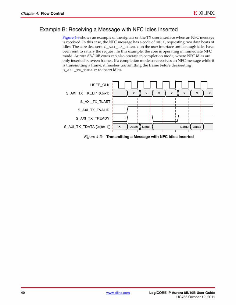
Example B: Receiving a Message with NFC Idles InsertedFigure 4-3 shows an example of the signals on the TX user interface when an NFC message is received. In this case, the NFC message has a code of 0001, requesting two data beats of idles. The core deasserts S_AXI_TX_TREADY on the user interface until enough idles have been sent to satisfy the request. In this example, the core is operating in immediate NFC mode. Aurora 8B/10B cores can also operate in completion mode, where NFC idles are only inserted between frames. If a completion mode core receives an NFC message while it is transmitting a frame, it finishes transmitting the frame before deasserting S_AXI_TX_TREADY to insert idles. X-Ref Target - Figure 4-3
Figure 4-3: Transmitting a Message with NFC Idles Inserted
40 www.xilinx.com LogiCORE IP Aurora 8B/10B User GuideUG766 October 19, 2011

User Flow Control
User Flow ControlThe Aurora 8B/10B protocol includes user flow control (UFC) to allow channel partners to send control information using a separate in-band channel. The user can send short UFC messages to the core's channel partner without waiting for the end of a frame in progress. The UFC message shares the channel with regular frame data, but has a higher priority.
Table 4-3 describes the ports for the UFC interface.
Table 4-3: UFC I/O Ports
Name Direction Description
S_AXI_UFC_TX_REQ Input
Asserted to request a UFC message be sent to the channel partner (active-High). Must be held until S_AXI_UFC_TX_ACK is asserted. Do not assert this signal unless the entire UFC message is ready to be sent; a UFC message cannot be interrupted after it has started.
S_AXI_UFC_TX_MS[0:2] InputSpecifies the size of the UFC message that is sent. The SIZE encoding is a value between 0 and 7. See Table 4-4, page 42.
S_AXI_UFC_TX_ACK Output
Asserted when an Aurora 8B/10B core is ready to read the contents of the UFC message (active-High). On the cycle after the S_AXI_UFC_TX_ACK signal is asserted, data on the S_AXI_TX_TDATA port is treated as UFC data. S_AXI_TX_TDATA data continues to be used to fill the UFC message until enough cycles have passed to send the complete message. Unused bytes from a UFC cycle are discarded.
M_AXI_UFC_RX_TDATA[0:(8n-1)] OutputIncoming UFC message data from the channel partner (n = 16 bytes maximum).
M_AXI_UFC_RX_TVALID OutputAsserted when the values on the M_AXI_UFC_RX ports are valid. When this signal is not asserted, all values on the M_AXI_UFC_RX ports should be ignored (active-High).
M_AXI_UFC_RX_TLAST Output Signals the end of the incoming UFC message (active-High).
M_AXI_UFC_RX_TKEEP[0:(n-1)] Output
Specifies the number of valid bytes of data presented on the M_AXI_UFC_RX_TDATA port on the last word of a UFC message. Valid only when M_AXI_UFC_RX_TLAST is asserted (n = 16 bytes maximum).
LogiCORE IP Aurora 8B/10B User Guide www.xilinx.com 41UG766 October 19, 2011

Chapter 4: Flow Control
Transmitting UFC MessagesUFC messages can carry an even number of data bytes from 2 to 16. The user application specifies the length of the message by driving a SIZE code on the S_AXI_UFC_TX_MS port. Table 4-4 shows the legal SIZE code values for UFC.
To send a UFC message, the user application asserts S_AXI_UFC_TX_REQ while driving the S_AXI_UFC_TX_MS port with the desired SIZE code. S_AXI_UFC_TX_REQ must be held until the Aurora 8B/10B core asserts the S_AXI_UFC_TX_ACK signal, indicating that the core is ready to send the UFC message. The data for the UFC message must be placed on the S_AXI_TX_TDATA port of the data interface, starting on the first cycle after S_AXI_UFC_TX_ACK is asserted. The core deasserts S_AXI_TX_TREADY while the S_AXI_TX_TDATA port is being used for UFC data.
Figure 4-4 shows a useful circuit for switching TX_D from sending regular data to UFC data.
Table 4-5, page 43 shows the number of cycles required to transmit UFC messages of different sizes based on the width of the AXI4-Stream data interface. UFC messages should never be started until all message data is available. Unlike regular data, UFC messages cannot be interrupted after S_AXI_UFC_TX_ACK has been asserted.
Table 4-4: SIZE Encoding
SIZE Field Contents UFC Message Size
000 2 bytes
001 4 bytes
010 6 bytes
011 8 bytes
100 10 bytes
101 12 bytes
110 14 bytes
111 16 bytes
X-Ref Target - Figure 4-4
Figure 4-4: Data Switching Circuit
Regular Data
UFC Data
S_AXI_TX_TREADY
S_AXI_TX_TDATA
0
1
UFC Interface
Data Interface
UG766_05_04_011811
Aurora 8B/10B Core
42 www.xilinx.com LogiCORE IP Aurora 8B/10B User GuideUG766 October 19, 2011

User Flow Control
Table 4-5: Number of Data Beats Required to Transmit UFC Messages
UFC MessageS_AXI_UFC_TX_MS
ValueAXI4 Interface
WidthNumber of Data Beats
AXI4 Interface Width
Number of Data Beats
2 Bytes 0
2 Bytes
1
10 Bytes
1
4 Bytes 1 2
6 Bytes 2 3
8 Bytes 3 4
10 Bytes 4 5
12 Bytes 5 6
214 Bytes 6 7
16 Bytes 7 8
2 Bytes 0
4 Bytes
1
12 Bytes
1
4 Bytes 1
6 Bytes 22
8 Bytes 3
10 Bytes 43
12 Bytes 5
14 Bytes 64 2
16 Bytes 7
2 Bytes 0
6 Bytes
1
14 Bytes1
4 Bytes 1
6 Bytes 2
8 Bytes 3
210 Bytes 4
12 Bytes 5
14 Bytes 63
16 Bytes 7 2
2 Bytes 0
8 Bytes
1
16 Bytes or more
1
4 Bytes 1
6 Bytes 2
8 Bytes 3
10 Bytes 4
212 Bytes 5
14 Bytes 6
16 Bytes 7
LogiCORE IP Aurora 8B/10B User Guide www.xilinx.com 43UG766 October 19, 2011
Chapter 4: Flow Control
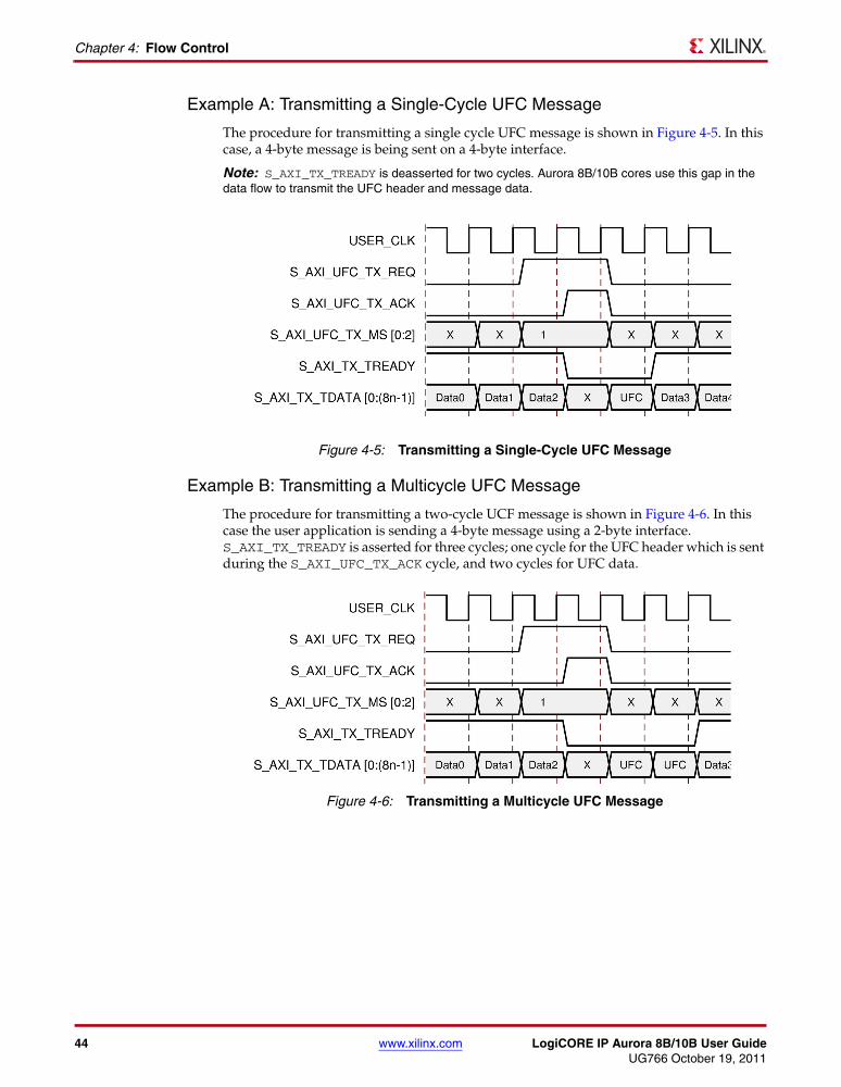
Example A: Transmitting a Single-Cycle UFC Message
The procedure for transmitting a single cycle UFC message is shown in Figure 4-5. In this case, a 4-byte message is being sent on a 4-byte interface.
Note: S_AXI_TX_TREADY is deasserted for two cycles. Aurora 8B/10B cores use this gap in the data flow to transmit the UFC header and message data.
Example B: Transmitting a Multicycle UFC Message
The procedure for transmitting a two-cycle UCF message is shown in Figure 4-6. In this case the user application is sending a 4-byte message using a 2-byte interface. S_AXI_TX_TREADY is asserted for three cycles; one cycle for the UFC header which is sent during the S_AXI_UFC_TX_ACK cycle, and two cycles for UFC data.
X-Ref Target - Figure 4-5
Figure 4-5: Transmitting a Single-Cycle UFC Message
X-Ref Target - Figure 4-6
Figure 4-6: Transmitting a Multicycle UFC Message
44 www.xilinx.com LogiCORE IP Aurora 8B/10B User GuideUG766 October 19, 2011

User Flow Control
Receiving User Flow Control MessagesWhen the Aurora 8B/10B core receives a UFC message, it passes the data from the message to the user application through a dedicated UFC AXI4-Stream interface. The data is presented on the M_AXI_UFC_RX_TDATA port; M_AXI_UFC_RX_TVALID indicates the start of the message data and M_AXI_UFC_RX_TLAST indicates the end. M_AXI_UFC_RX_TKEEP is used to show the number of valid bytes on M_AXI_UFC_RX_TDATA during the last cycle of the message (for example, while M_AXI_UFC_RX_TLAST is asserted). Signals on the M_AXI_UFC_RX AXI4-Stream interface are only valid when M_AXI_UFC_RX_TVALID is asserted.
Example C: Receiving a Single-Cycle UFC Message
Figure 4-7 shows an Aurora 8B/10B core with a 4-byte data interface receiving a 4-byte UFC message. The core presents this data to the user application by asserting M_AXI_UFC_RX_TVALID and M_AXI_UFC_RX_TLAST to indicate a single cycle frame. M_AXI_UFC_RX_TKEEP is set to 4'hF, indicating only the four most significant bytes of the interface are valid.
Example D: Receiving a Multicycle UFC Message
Figure 4-8 shows an Aurora 8B/10B core with a 4-byte interface receiving an 8-byte message.
Note: The resulting frame is two cycles long, with M_AXI_UFC_RX_TKEEP set to 4'hF on the second cycle indicating that all four bytes of the data are valid.
X-Ref Target - Figure 4-7
Figure 4-7: Receiving a Single-Cycle UFC Message
X-Ref Target - Figure 4-8
Figure 4-8: Receiving a Multicycle UFC Message
LogiCORE IP Aurora 8B/10B User Guide www.xilinx.com 45UG766 October 19, 2011

Chapter 4: Flow Control
46 www.xilinx.com LogiCORE IP Aurora 8B/10B User GuideUG766 October 19, 2011

Chapter 5
Status, Control, and the Transceiver Interface
IntroductionThe status and control ports of the Aurora 8B/10B core allow user applications to monitor the Aurora 8B/10B channel and use built-in features of the GTP/GTX transceivers. Aurora 8B/10B cores can be configured as full-duplex or simplex modules. Full-duplex modules provide high-speed TX and RX links. Simplex modules provide a link in only one direction and are initialized using sideband ports or with a built-in timer. This chapter provides diagrams and port descriptions for the Aurora 8B/10B core’s status and control interface, along with the GTP/GTX transceiver serial I/O interface and the sideband initialization ports that are used exclusively for simplex modules. X-Ref Target - Figure 5-1
Figure 5-1: Top-Level Transceiver Interface
TX Data
Control
Control
TXP/TXN
NFC Number of Idles
NFC Req
UFC TX Message Size
UFC TX Req
UFC TX Data
ClockingClock Module-Chapter 7-
GTP Interface-Chapter 6-
Clock Interface-Chapter 7-
User Interface-Chapter 4-
Aurora 8B/10B Module
Native Flow Control(NFC) Interface
-Chapter 5-
User Flow Control(UFC) Interface
-Chapter 5-
Do CC
Warn CCClockCompensation
Module-Chapter 8-
ClockCompensation
-Chapter 8-
Status
Status
RXP/RXN
RX Data
NFC Ack
UFC RX Data
UFC RX Status/Ctrl
UFC TX Ack
Clocking
UG766_06_01_080411
TX Data
Control
Control
TXP/TXN
NFC Number of Idles
NFC Req
UFC TX Message Size
UFC TX Req
UFC TX Data
ClockingClock Module-Chapter 6-
Transceiver Interface-Chapter 5-
Clock Interface-Chapter 6-
User Interface-Chapter 3-
Native Flow Control(NFC) Interface
-Chapter 4-
User Flow Control(UFC) Interface
-Chapter 4-
Do CC
Warn CCClockCompensation
Module-Chapter 7-
ClockCompensation
-Chapter 7-
Status
Status
RXP/RXN
RX Data
NFC Ack
UFC RX Data
UFC RX Status/Ctrl
UFC TX Ack
Clocking
LogiCORE IP Aurora 8B/10B User Guide www.xilinx.com 47UG766 October 19, 2011

Chapter 5: Status, Control, and the Transceiver Interface
Full-Duplex Cores
Full-Duplex Status and Control PortsFull-duplex cores provide a TX and an RX Aurora 8B/10B channel connection. Figure 5-2 shows the status and control interface for a full-duplex Aurora 8B/10B core. Table 5-1 describes the function of each of the ports in the interface.X-Ref Target - Figure 5-2
Figure 5-2: Status and Control Interface for Full-Duplex Cores
Table 5-1: Status and Control Ports for Full-Duplex Cores
Name Direction Description
CHANNEL_UP Output
Asserted when Aurora 8B/10B channel initialization is complete and channel is ready to send data. The Aurora 8B/10B core cannot receive data before CHANNEL_UP.
LANE_UP[0:m-1] Output
Asserted for each lane upon successful lane initialization, with each bit representing one lane (active-High). The Aurora 8B/10B core can only receive data after all LANE_UP signals are High.
FRAME_ERR OutputChannel frame/protocol error detected. This port is active-High and is asserted for a single clock.
HARD_ERR OutputHard error detected. (Active High, asserted until Aurora 8B/10B core resets). See Error Signals in Full-Duplex Cores, page 49 for more details.
LOOPBACK[2:0] Input
The LOOPBACK[2:0] port selects between the normal operation mode and the different loopback modes. See the 7 Series FPGAs GTX Transceivers User Guide, Virtex-6 FPGA GTX Transceivers User Guide, or the Spartan-6 FPGA GTP Transceivers User Guide for details about loopback. See Introduction in Chapter 1.
POWER_DOWN InputDrives the power-down input of the GTP/GTX transceiver (active-High).
RESET InputResets the Aurora 8B/10B core (active High). This signal must be synchronous to USER_CLK and must be asserted for at least one USER_CLK cycle.
HARD_ERR
SOFT_ERR
FRAME_ERR
LANE_UP[0:m-1]
CHANNEL_UP
LOOPBACK[2:0]
POWER_DOWN
RESET Full-DuplexStatus and
ControlInterface
GT_RESET
INIT_CLK
TXP[0:m-1]
TXN[0:m-1]
RXP[0:m-1]
RXN[0:m-1]
UG766_06_02_072610
48 www.xilinx.com LogiCORE IP Aurora 8B/10B User GuideUG766 October 19, 2011

Full-Duplex Cores
Error Signals in Full-Duplex CoresEquipment problems and channel noise can cause errors during Aurora 8B/10B channel operation. 8B/10B encoding allows the Aurora 8B/10B core to detect all single bit errors and most multi-bit errors that occur in the channel. The core reports these errors by asserting the SOFT_ERR signal on every cycle they are detected.
The core also monitors each GTP/GTX transceiver for hardware errors such as buffer overflow/underflow and loss of lock. The core reports hardware errors by asserting the HARD_ERR signal. Catastrophic hardware errors can also manifest themselves as burst of soft errors. The core uses the leaky bucket algorithm described in the Aurora 8B/10B Protocol Specification to detect large numbers of soft errors occurring in a short period of time, and asserts the HARD_ERR signal when it detects them.
Whenever a hard error is detected, the Aurora 8B/10B core automatically resets itself and attempts to reinitialize. In most cases, this allows the Aurora 8B/10B channel to be reestablished as soon as the hardware issue that caused the hard error is resolved. Soft
SOFT_ERR Output
Soft error detected in the incoming serial stream. See Error Signals in Full-Duplex Cores, page 49 for more details. (Active-High, asserted for a single clock).
RXP[0:m-1] Input Positive differential serial data input pin.
RXN[0:m-1] Input Negative differential serial data input pin.
TXP[0:m-1] Output Positive differential serial data output pin.
TXN[0:m-1] Output Negative differential serial data output pin.
GT_RESET Input
The reset signal for the PMA modules in the transceivers is connected to the top level through a debouncer. The GT_RESET port should be asserted (active-High) when the module is first powered up in hardware. This systematically resets all PCS and PMA subcomponents of the transceiver.
The signal is debounced using INIT_CLK.
See the Reset section in the respective transceiver user guide for further details.
INIT_CLK Input
INIT_CLK is used to register and debounce the GT_RESET signal. INIT_CLK is required because USER_CLK stops when GT_RESET is asserted. INIT_CLK should be set to a slow rate, preferably slower than the reference clock. INIT_CLK is a board clock. For example, the ML623 board has a 200 MHz crystal oscillator, and it is constrained for this frequency by default in <component name>_example_design.ucf. Users need to update this clock constraint with respect to their board clock frequency.
Notes: 1. m is the number of GTP/GTX transceivers
Table 5-1: Status and Control Ports for Full-Duplex Cores (Cont’d)
Name Direction Description
LogiCORE IP Aurora 8B/10B User Guide www.xilinx.com 49UG766 October 19, 2011

Chapter 5: Status, Control, and the Transceiver Interface
errors do not lead to a reset unless enough of them occur in a short period of time to trigger the Aurora 8B/10B leaky bucket algorithm.
Aurora 8B/10B cores with a AXI4-Stream data interface can also detect errors in Aurora 8B/10B frames. Errors of this type include frames with no data, consecutive Start of Frame symbols, and consecutive End of Frame symbols. When the core detects a frame problem, it asserts the FRAME_ERR signal. This signal is usually asserted close to a SOFT_ERR assertion, with soft errors being the main cause of frame errors.
Table 5-2 summarizes the error conditions the Aurora 8B/10B core can detect and the error signals used to alert the user application.
Table 5-2: Error Signals in Full-Duplex Cores
Signal Description
HARD_ERR
TX Overflow/Underflow: The elastic buffer for TX data overflows or underflows. This can occur when the user clock and the reference clock sources are not running at the same frequency.
RX Overflow/Underflow: The elastic buffer for RX data overflows or underflows. This can occur when the clock source frequencies for the two channel partners are not within ± 100 ppm.
Bad Control Character: The protocol engine attempts to send a bad control character. This is an indication of design corruption or catastrophic failure.
Soft Errors: There are too many soft errors within a short period of time. The Aurora 8B/10B protocol defines a leaky bucket algorithm for determining the acceptable number of soft errors within a given time period. When this number is exceeded, the physical connection might be too poor for communication using the current voltage swing and pre-emphasis settings.
SOFT_ERR
Invalid Code: The 10-bit code received from the channel partner was not a valid code in the 8B/10B table. This usually means a bit was corrupted in transit, causing a good code to become unrecognizable. Typically, this also results in a frame error or corruption of the current channel frame.
Disparity Error: The 10-bit code received from the channel partner did not have the correct disparity. This error is also usually caused by corruption of a good code in transit, and can result in a frame error or bad data if it occurs while a frame is being sent.
FRAME_ERR
Truncated Frame: A channel frame is started without ending the previous channel frame, or a channel frame is ended without being started.
Invalid Control Character: The protocol engine receives a control character that it does not recognize.
No Data in Frame: A channel frame is received with no data.
50 www.xilinx.com LogiCORE IP Aurora 8B/10B User GuideUG766 October 19, 2011

Simplex Cores
Full-Duplex InitializationFull-duplex cores initialize automatically after power up, reset, or hard error. Full-duplex modules on each side of the channel perform the Aurora 8B/10B initialization procedure until the channel is ready for use. The LANE_UP bus indicates which lanes in the channel have finished the lane initialization portion of the initialization procedure. This signal can be used to help debug equipment problems in a multi-lane channel. CHANNEL_UP is asserted only after the core completes the entire initialization procedure.
Aurora 8B/10B cores cannot receive data before CHANNEL_UP is asserted. Only the M_AXI_RX_TVALID signal on the user interface should be used to qualify incoming data. CHANNEL_UP can be inverted and used to reset modules that drive the TX side of a full-duplex channel, because no transmission can occur until after CHANNEL_UP. If user application modules need to be reset before data reception, one of the LANE_UP signals can be inverted and used. Data cannot be received until after all the LANE_UP signals are asserted.
Simplex Cores
Simplex TX Status and Control PortsSimplex TX cores allow user applications to transmit data to a simplex RX core. They have no RX connection. Figure 5-3 shows the status and control interface for a simplex TX core. Table 5-3 describes the function of each of the ports in the interface. X-Ref Target - Figure 5-3
Figure 5-3: Status and Control Interface for Simplex TX Core
Table 5-3: Status and Control Ports for Simplex TX Cores
Name Direction Description
TX_ALIGNED InputAsserted when RX channel partner has completed lane initialization for all lanes. Typically connected to RX_ALIGNED.
TX_BONDED Input
Asserted when RX channel partner has completed channel bonding. Not needed for single-lane channels. Typically connected to RX_BONDED.
TX_VERIFY InputAsserted when RX channel partner has completed verification. Typically connected to RX_VERIFY.
Simplex TXStatus and
ControlInterface
TX_ALIGNED
TX_BONDED
TX_VERIFY
TX_RESET
TX_HARD_ERR
TX_LANE_UP[0:m-1]
TX_CHANNEL_UP
POWER_DOWN
TX_SYSTEM_RESET
TXP[0:m-1]
TXN[0:m-1]UG766_06_03_072610
LogiCORE IP Aurora 8B/10B User Guide www.xilinx.com 51UG766 October 19, 2011

Chapter 5: Status, Control, and the Transceiver Interface
Simplex RX Status and Control PortsSimplex RX cores allow user applications to receive data from a simplex TX core. Figure 5-4 shows the status and control interface for a simplex RX core. Table 5-4 describes the function of each of the ports in the interface.
TX_RESET Input
Asserted when reset is required because of initialization status of RX channel partner. This signal must be synchronous to USER_CLK and must be asserted for at least one USER_CLK cycle. Typically connected to RX_RESET.
TX_CHANNEL_UP Output
Asserted when Aurora 8B/10B channel initialization is complete and channel is ready to send data. The Aurora 8B/10B core cannot receive data before TX_CHANNEL_UP.
TX_LANE_UP[0:m-1] OutputAsserted for each lane upon successful lane initialization, with each bit representing one lane (active-High).
TX_HARD_ERR Output
Hard error detected. (Active-High, asserted until Aurora 8B/10B core resets). See Error Signals in Simplex Cores, page 54 for more details.
POWER_DOWN InputDrives the powerdown input of the GTP/GTX transceiver (active-High).
TX_SYSTEM_RESET Input Resets the Aurora 8B/10B core (active-High).
TXP[0:m-1] Output Positive differential serial data output pin.
TXN[0:m-1] Output Negative differential serial data output pin.
Notes: 1. m is the number of GTP/GTX transceivers.
Table 5-3: Status and Control Ports for Simplex TX Cores (Cont’d)
Name Direction Description
X-Ref Target - Figure 5-4
Figure 5-4: Status and Control Interface for Simplex RX Core
Simplex RXStatus and
ControlInterface RX_ALIGNED
RX_BONDED
RX_VERIFY
RX_RESET
RX_HARD_ERR
SOFT_ERR
FRAME_ERR
RX_LANE_UP[0:m-1]
RX_CHANNEL_UP
POWER_DOWN
RX_SYSTEM_RESET
RXP[0:m-1]
RXN[0:m-1]
UG766_06_04_072610
52 www.xilinx.com LogiCORE IP Aurora 8B/10B User GuideUG766 October 19, 2011

Simplex Cores
Table 5-4: Status and Control Ports for Simplex RX Cores
Name Direction Description
RX_ALIGNED OutputAsserted when RX module has completed lane initialization. Typically connected to TX_ALIGNED.
RX_BONDED OutputAsserted when RX module has completed channel bonding. Not used for single-lane channels. Typically connected to TX_BONDED.
RX_VERIFY OutputAsserted when RX module has completed verification. Typically connected to TX_VERIFY.
RX_RESET OutputAsserted when the RX module needs the TX module to restart initialization. Typically connected to TX_RESET.
RX_CHANNEL_UP Output
Asserted when Aurora 8B/10B channel initialization is complete and channel is ready to send data. The Aurora 8B/10B core cannot receive data before RX_CHANNEL_UP.
RX_LANE_UP[0:m-1] Output
Asserted for each lane upon successful lane initialization, with each bit representing one lane (active-High). The Aurora 8B/10B core can only receive data after all RX_LANE_UP signals are High.
FRAME_ERR OutputChannel frame/protocol error detected. This port is active-High and is asserted for a single clock.
RX_HARD_ERR Output
Hard error detected. (Active-High, asserted until Aurora 8B/10B core resets). See Error Signals in Simplex Cores, page 54 for more details.
POWER_DOWN InputDrives the power-down input of the GTP/GTX transceiver (active-High).
RX_SYSTEM_RESET Input Resets the Aurora 8B/10B core (active-High).
SOFT_ERR Output
Soft error detected in the incoming serial stream. See Error Signals in Simplex Cores, page 54 for more details. (Active-High, asserted for a single clock).
RXP[0:m-1] Input Positive differential serial data input pin.
RXN[0:m-1] Input Negative differential serial data input pin.
Notes: 1. m is the number of GTP/GTX transceivers.2. RX_ALIGNED, RX_BONDED, RX_VERIFY, and RX_RESET are available as output signals even when the
simplex partner is timer based, but functionally these signals are not required.
LogiCORE IP Aurora 8B/10B User Guide www.xilinx.com 53UG766 October 19, 2011

Chapter 5: Status, Control, and the Transceiver Interface
Error Signals in Simplex CoresThe 8B/10B encoding allows RX simplex cores to detect all single bit errors and most multi-bit errors in a simplex channel. The cores report these errors by asserting the SOFT_ERR signal on every cycle an error is detected. The TX simplex cores do not include a SOFT_ERR port. All transmit data is assumed correct at transmission unless there is an equipment problem.
All simplex cores monitor their GTP/GTX transceivers for hardware errors such as buffer overflow/underflow and loss of lock. Hardware errors on the TX side of the channel are reported by asserting the TX_HARD_ERR signal; RX side hard errors are reported using the RX_HARD_ERR signal. Simplex RX cores use the Aurora 8B/10B protocol's leaky bucket algorithm to evaluate bursts of soft errors. If too many soft errors occur in a short span of time, RX_HARD_ERR is asserted.
Whenever a hard error is detected, the Aurora 8B/10B core automatically resets itself and attempts to reinitialize. Resetting allows the Aurora 8B/10B channel to be re-established as soon as the hardware issue that caused the hard error is resolved in most cases. Soft errors do not lead to a reset unless enough of them occur in a short period of time to trigger the Aurora 8B/10B leaky bucket algorithm.
Simplex RX cores with a AXI4-Stream data interface can also detect errors in Aurora 8B/10B frames when they are received. Errors of this type include frames with no data, consecutive Start of Frame symbols, and consecutive End of Frame symbols. When the core detects a frame problem, it asserts the FRAME_ERR signal. This signal is usually asserted close to a SOFT_ERR assertion, as soft errors are the main cause of frame errors. Simplex TX modules do not use the FRAME_ERR port.
Table 5-5 summarizes the error conditions simplex Aurora 8B/10B cores can detect and the error signals uses to alert the user application.
Table 5-5: Error Signals in Simplex Cores
Signal Description TX RX
HARD_ERR
TX Overflow/Underflow: The elastic buffer for TX data overflows or underflows. This can occur when the user clock and the reference clock sources are not running at the same frequency.
x
RX Overflow/Underflow: The elastic buffer for RX data overflows or underflows. This can occur when the clock source frequencies for the two channel partners are not within ± 100 ppm.
x
Bad Control Character: The protocol engine attempts to send a bad control character. This is an indication of design corruption or catastrophic failure.
x
Soft Errors: There are too many soft errors within a short period of time. The Aurora 8B/10B protocol defines a leaky bucket algorithm for determining the acceptable number of soft errors within a given time period. When this number is exceeded, the physical connection might be too poor for communication using the current voltage swing and pre-emphasis settings.
x
54 www.xilinx.com LogiCORE IP Aurora 8B/10B User GuideUG766 October 19, 2011

Simplex Cores
Simplex InitializationSimplex cores do not depend on signals from an Aurora 8B/10B channel for initialization. Instead, the TX and RX sides of simplex channels communicate their initialization state through a set of sideband initialization signals. The initialization ports are called ALIGNED, BONDED, VERIFY, and RESET; one set for the TX side with a TX_ prefix, and one set for the RX side with an RX_ prefix. The bonded port is only used for multi-lane cores.
There are two ways to initialize a simplex module using the sideband initialization signals:
• Send the information from the RX sideband initialization ports to the TX sideband initialization ports
• Drive the TX sideband initialization ports independently of the RX sideband initialization ports using timed initialization intervals
Both initialization methods are described in the following sections.
Using a Back Channel
If there is no communication channel available from the RX side of the connection to the TX side, using a back channel is the safest way to initialize and maintain a simplex channel. There are very few requirements on the back channel; it need only deliver messages to the TX side to indicate which of the sideband initialization signals is asserted when the signals change.
The Aurora example design included in the example_design directory with simplex Aurora 8B/10B cores shows a simple side channel that uses 3 or 4 I/O pins on the device.
SOFT_ERR
Invalid Code: The 10-bit code received from the channel partner was not a valid code in the 8B/10B table. This usually means a bit was corrupted in transit, causing a good code to become unrecognizable. Typically, this also results in a frame error or corruption of the current channel frame.
x
Disparity Error: The 10-bit code received from the channel partner did not have the correct disparity. This error is also usually caused by corruption of a good code in transit, and can result in a frame error or bad data if it occurs while a frame is being sent.
x
No Data in Frame: A channel frame is received with no data. x
FRAME_ERR
Truncated Frame: A channel frame is started without ending the previous channel frame, or a channel frame is ended without being started.
x
Invalid Control Character: The protocol engine receives a control character that it does not recognize.
x
Invalid UFC Message Length: A UFC message is received with an invalid length. x
Table 5-5: Error Signals in Simplex Cores (Cont’d)
Signal Description TX RX
LogiCORE IP Aurora 8B/10B User Guide www.xilinx.com 55UG766 October 19, 2011

Chapter 5: Status, Control, and the Transceiver Interface
Using Timers
For some systems a back channel is not possible. In these cases, serial channels can be initialized by driving the TX simplex initialization with a set of timers. The timers must be designed carefully to meet the needs of the system because the average time for initialization depends on many channel specific conditions such as clock rate, channel latency, skew between lanes, and noise. C_ALIGNED_TIMER, C_BONDED_TIMER, and C_VERIFY_TIMER are timers used for assertion of TX_ALIGNED, TX_BONDED, and TX_VERIFY signals, respectively. These timers use worst-case values obtained from corner case functional simulations and implemented in the <component name> module.
Some of the initialization logic in the Aurora 8B/10B module uses watchdog timers to prevent deadlock. These watchdog timers are used on the RX side of the channel, and can interfere with the proper operation of TX initialization timers. If the RX simplex module goes from ALIGNED, BONDED or VERIFY, to RESET, make sure that it is not because the TX logic spend too much time in one of those states. If a particularly long timer is required to meet the needs of the system, the watchdog timers can be adjusted by editing the lane_init_sm module and the channel_init_sm module. For most cases, this should not be necessary and is not recommended.
Aurora 8B/10B channels normally reinitialize only in the case of failure. When there is no back channel available, event-triggered re-initialization is impossible for most errors because it is usually the RX side that detects a failure and the TX side that must handle it. The solution for this problem is to make timer-driven TX simplex modules reinitialize on a regular basis. If a catastrophic error occurs, the channel is reset and running again after the next re-initialization period arrives. System designers should balance the average time required for re-initialization against the maximum time their system can tolerate an inoperative channel to determine the optimum re-initialization period for their systems.
Reset and Power Down
ResetThe reset signals on the control and status interface are used to set the Aurora 8B/10B core to a known starting state. Resetting the core stops any channels that are currently operating; after reset, the core attempts to initialize a new channel.
On full-duplex modules, the RESET signal resets both the TX and RX sides of the channel when asserted on the positive edge of USER_CLK. On simplex modules, the resets for the TX and RX channels are separate. TX_SYSTEM_RESET resets TX channels; RX_SYSTEM_RESET resets RX channels. The TX_SYSTEM_RESET is separate from the TX_RESET and RX_RESET signals used on the simplex sideband interface.
Power DownThis is an active-High signal. When POWER_DOWN is asserted, the GTP/GTX transceivers in the Aurora 8B/10B core are turned off, putting them into a non-operating low-power mode. When POWER_DOWN is deasserted, the core automatically resets. Be careful when asserting this signal on cores that use TX_OUT_CLK (see the Chapter 6, Clock Interface and Clocking). TX_OUT_CLK stops when the GTP/GTX transceivers are powered down. See the 7 Series FPGAs GTX Transceivers User Guide, the Virtex-6 FPGA GTX Transceivers User Guide, or the Spartan-6 FPGA GTP Transceivers User Guide for the device being used for details about powering down GTP/GTX transceivers.
56 www.xilinx.com LogiCORE IP Aurora 8B/10B User GuideUG766 October 19, 2011

Reset and Power Down
TimingFigure 5-5 shows the timing for the RESET and POWER_DOWN signals. In a quiet environment, tCU is generally less than 800 clocks; in a noisy environment, tCU can be much longer.X-Ref Target - Figure 5-5
Figure 5-5: Reset and Power Down Timing
USER_CLK
RESET, POWER_DOWN
CHANNEL_UP
t1 t2 t3 t4 tcutcu-1
UG766_06_06_072610
LogiCORE IP Aurora 8B/10B User Guide www.xilinx.com 57UG766 October 19, 2011

Chapter 5: Status, Control, and the Transceiver Interface
58 www.xilinx.com LogiCORE IP Aurora 8B/10B User GuideUG766 October 19, 2011

Chapter 6
Clock Interface and Clocking
IntroductionGood clocking is critical for the correct operation of the Aurora 8B/10B core. The core requires a high-quality, low-jitter reference clock to drive the high-speed TX clock and clock recovery circuits in the GTP/GTX transceivers. It also requires at least one frequency locked parallel clock for synchronous operation with the user application.
The Virtex®-7/Kintex™-7/Virtex-6 FPGA has four GTX transceivers in a Quad. The Spartan ®-6 FPGA GTP architecture has a pair of transceivers in each GTPA1_DUAL tile. The Virtex-7/Kintex-7/Virtex-6 FPGA GTX transceiver has individual PLLs for both TX and RX portion of the transceivers. The Spartan-6 FPGA has individual PLLs for each transceiver in a GTPA1_DUAL tile. The reference clock is used to produce the PLL clock, which is divided to make individual TX and RX serial clocks and parallel clocks in each GTP/GTX transceiver.
Each Aurora 8B/10B core is generated in the example_design directory that includes a design called aurora_example. This design by instantiating the generated Aurora 8B/10B core, demonstrates a working clock configuration of the core. First-time users should examine the Aurora example design and use it as a template when connecting the clock interface.
LogiCORE IP Aurora 8B/10B User Guide www.xilinx.com 59UG766 October 19, 2011

Chapter 6: Clock Interface and Clocking
X-Ref Target - Figure 6-1
Figure 6-1: Top-Level Clocking
TX Data
Control
Control
TXP/TXN
NFC Number of Idles
NFC Req
UFC TX Message Size
UFC TX Req
UFC TX Data
ClockingClock Module-Chapter 6-
GTP/GTX Interface-Chapter 5-
Clock Interface-Chapter 6-
User Interface-Chapter 3-
Aurora 8B/10B Module
Native Flow Control(NFC) Interface
-Chapter 4-
User Flow Control(UFC) Interface
-Chapter 4-
Do CC
Warn CCClockCompensation
Module-Chapter 7-
ClockCompensation
-Chapter 7-
Status
Status
RXP/RXN
RX Data
NFC Ack
UFC RX Data
UFC RX Status/Ctrl
UFC TX Ack
Clocking
UG766_07_01_072610
60 www.xilinx.com LogiCORE IP Aurora 8B/10B User GuideUG766 October 19, 2011

Clock Interface Ports for GTP/GTX Transceiver Cores
Clock Interface Ports for GTP/GTX Transceiver CoresTable 6-1 describes the Aurora 8B/10B core clock ports.
Clocking from a Neighboring GTX_QUAD Tile for Virtex-6 FPGA Designs
The Xilinx implementation tools make necessary adjustments to the north-south routing shown in Figure 6-2, page 63 as well as pin swapping necessary to GTXE1 clock inputs to route clocks from one Quad to another when required.
The following rules must be observed when sharing a reference clock to ensure that jitter margins for high-speed designs are met:
1. The number of GTX Quads above the sourcing Quad must not exceed one.
Table 6-1: Clock Ports for a GTP/GTX Aurora 8B/10B Core
Clock Ports Direction Description
PLL_NOT_LOCKED Input
If a PLL is used to generate clocks for the Aurora 8B/10B core, the PLL_NOT_LOCKED signal should be connected to the inverse of the PLL's LOCKED signal. The clock module provided with the Aurora 8B/10B core uses the PLL for clock division. The PLL_NOT_LOCKED signal from the clock module should be connected to the PLL_NOT_LOCKED signal on the Aurora 8B/10B core. If the PLL is not used to generate clock signals for the Aurora 8B/10B core, tie PLL_NOT_LOCKED to ground.
USER_CLK Input
Parallel clock shared by the Aurora 8B/10B core and the user application. In Aurora 8B/10B cores, USER_CLK and SYNC_CLK are the outputs of a PLL whose input is derived from TX_OUT_CLK. These clock generations are available in <component name>_clock_module file. The Spartan-6 FPGA uses the GTPCLKOUT port to derive USER_CLK and SYNC_CLK outputs. USER_CLK goes as the TXUSRCLK2 input to the transceiver. See the respective transceiver user guide for more information.
SYNC_CLK Input
Parallel clock used by the internal synchronization logic of the GTP/GTX transceivers in the Aurora 8B/10B core. SYNC_CLK goes as the TXUSRCLK input to the transceiver. See the respective transceiver user guide for more information.
GT_REFCLK Input
GT_REFCLK (CLKP/CLKN) is a dedicated external clock generated from an oscillator. This clock is fed through IBUFDS. To minimize the number of oscillators, the GTP/GTX transceiver architecture has a NORTH/SOUTH clock routing matrix using CLKP/CLKN.
CPLLLOCKDETCLK_IN Input
CPLLLOCKDETCLK pin of the GTXE2 Transceiver module. See the 7 Series FPGAs GTX Transceivers User Guide for more information. Available only for Virtex-7/Kintex-7 device-based designs.
LogiCORE IP Aurora 8B/10B User Guide www.xilinx.com 61UG766 October 19, 2011

Chapter 6: Clock Interface and Clocking
2. The number of GTX Quads below the sourcing Quad must not exceed one.
3. The total number of GTX Quads sourced by an external clock pin pair (MGTREFCLKN/MGTREFCLKP) must not exceed three or 12 GTXE1 transceivers.
The maximum number of GTX transceivers that can be sourced by a single clock pin pair is 12. Designs with more than 12 transceivers require the use of multiple external clock pins to ensure that the rules for controlling jitter are followed. When multiple clock pins are used, an external buffer can be used to drive them from the same oscillator.
Note: Virtex-7/Kintex-7 FPGA reference clock sharing guidelines are the same as the guidelines for Virtex-6 FPGAs.
62 www.xilinx.com LogiCORE IP Aurora 8B/10B User GuideUG766 October 19, 2011

Clocking from a Neighboring GTX_QUAD Tile for Virtex-6 FPGA Designs
X-Ref Target - Figure 6-2
Figure 6-2: North-South Routing Adjustments in Virtex-6 FPGAsUG766_07_05_072610
LogiCORE IP Aurora 8B/10B User Guide www.xilinx.com 63UG766 October 19, 2011

Chapter 6: Clock Interface and Clocking
Reference Clocks for Spartan-6 FPGA GTP Transceiver DesignsIn Spartan-6 FPGA transceiver designs, the reference clock is GTPD, which is a differential input clock for each GTPA1_DUAL. The reference clock for GTPA1_DUAL is provided through the CLK00 and CLK01 ports. The two possible use models for distributing a reference clock to drive the CLK00 and CLK01 ports are:
• Clocking from and External Source
• Clocking from a Neighboring GTPA1_DUAL Tile
Clocking from and External Source Each GTPA1_DUAL tile has a pair of dedicated pins that can be connected to an external clock source. To use these pins, a IBUFDS primitive is instantiated. In the user constraints file (.ucf), the IBUFDS input pins are set to the dedicated clock pins for the tile. In the design, the output of the IBUFDS is connected to the CLK00 and CLK01 ports. Each GTPA1_DUAL takes differential GTPD clock inputs, which are directly bonded to the FPGA pins. For multilane Aurora 8B/10B designs, GTPD clock of any GTPA1_DUAL can be used as the reference clock for the Aurora 8B/10B design. Using a low-jitter oscillator delivers a high-quality clock suitable for top-speed operation. Figure 6-3 shows a differential GTPA1_DUAL clock pin pair sourced by an external oscillator on the board. This clocking mechanism is used for Spartan-6 FPGA single lane and 2-lane designs.X-Ref Target - Figure 6-3
Figure 6-3: Single GTPA1_DUAL Tile Clocked Externally
CLK00 CLK01
BUFDS
UG766_07_06_072610
GTPA1_DUAL Tile
64 www.xilinx.com LogiCORE IP Aurora 8B/10B User GuideUG766 October 19, 2011

Clock Rates for GTP/GTX Transceiver Designs
Clocking from a Neighboring GTPA1_DUAL TileThe external clock from one tile can be used to drive the CLK00 and CLK01 ports of neighboring tiles.
The example in Figure 6-4 uses the clock from one GTPA1_DUAL tile to clock neighboring tiles. A GTPA1_DUAL tile shares its clock with its neighbors using dedicated clock routing resources. This clocking mechanism is used for Spartan-6 FPGA 4-lane design.
Clock Rates for GTP/GTX Transceiver DesignsGTP/GTX transceivers support a wide range of serial rates. The attributes used to configure the GTP/GTX transceivers in the Aurora 8B/10B core for a specific line rate are kept in the transceiver_wrapper module for simulation. These attributes are set automatically by the CORE Generator software in response to the line rate and reference clock selections made in the Configuration GUI window for the core. Manual edits of the attributes are not recommended, but are possible using the recommendations in the 7 Series FPGAs GTX Transceivers User Guide, Virtex-6 FPGA GTX Transceivers User Guide, and the Spartan-6 FPGA GTP Transceivers User Guide.
X-Ref Target - Figure 6-4
Figure 6-4: GTPA1_DUAL Tiles with Shared Reference Clock
CLK00 CLK01
BUFDS
UG766_07_07_072610
GTPA1_DUAL Tile
CLK00 CLK01
GTPA1_DUAL Tile
LogiCORE IP Aurora 8B/10B User Guide www.xilinx.com 65UG766 October 19, 2011

Chapter 6: Clock Interface and Clocking
66 www.xilinx.com LogiCORE IP Aurora 8B/10B User GuideUG766 October 19, 2011

Chapter 7
Clock Compensation
IntroductionClock compensation is a feature that allows up to ± 100 ppm difference in the reference clock frequencies used on each side of an Aurora 8B/10B channel. This feature is used in systems where a separate reference clock source is used for each device connected by the channel, and where the same USER_CLK is used for transmitting and receiving data.
The Aurora 8B/10B core’s clock compensation interface enables full control over the core's clock compensation features. A standard clock compensation module is generated with the Aurora 8B/10B core to provide Aurora 8B/10B-compliant clock compensation for systems using separate reference clock sources; users with special clock compensation requirements can drive the interface with custom logic. If the same reference clock source is used for both sides of the channel, the interface can be tied to ground to disable clock compensation.
LogiCORE IP Aurora 8B/10B User Guide www.xilinx.com 67UG766 October 19, 2011

Chapter 7: Clock Compensation
Clock Compensation InterfaceAll Aurora 8B/10B cores include a clock compensation interface for controlling the transmission of clock compensation sequences. Table 7-1 describes the function of the clock compensation interface ports.
X-Ref Target - Figure 7-1
Figure 7-1: Top-Level Clock CompensationUG766_08_01_072610
TX Data
Control
Control
TXP/TXN
NFC Number of Idles
NFC Req
UFC TX Message Size
UFC TX Req
UFC TX Data
ClockingClock Module-Chapter 6-
GTP/GTX Interface-Chapter 5-
Clock Interface-Chapter 6-
User Interface-Chapter 3-
Aurora 8B/10B Module
Native Flow Control(NFC) Interface
-Chapter 4-
User Flow Control(UFC) Interface
-Chapter 4-
Do CC
Warn CCClockCompensation
Module-Chapter 7-
ClockCompensation
-Chapter 7-
Status
Status
RXP/RXN
RX Data
NFC Ack
UFC RX Data
UFC RX Status/Ctrl
UFC TX Ack
Clocking
Table 7-1: Clock Compensation I/O Ports
Name Direction Description
DO_CC InputThe Aurora 8B/10B core sends CC sequences on all lanes on every clock cycle when this signal is asserted. Connects to the DO_CC output on the CC module.
WARN_CC Input
The Aurora 8B/10B core does not acknowledge UFC requests while this signal is asserted. It is used to prevent UFC messages from starting too close to CC events. Connects to the WARN_CC output on the CC module.
68 www.xilinx.com LogiCORE IP Aurora 8B/10B User GuideUG766 October 19, 2011
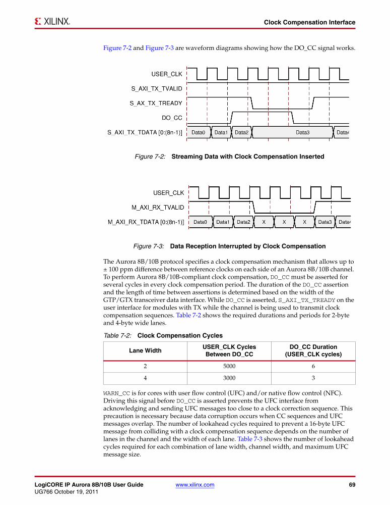
Clock Compensation Interface
Figure 7-2 and Figure 7-3 are waveform diagrams showing how the DO_CC signal works.
The Aurora 8B/10B protocol specifies a clock compensation mechanism that allows up to ± 100 ppm difference between reference clocks on each side of an Aurora 8B/10B channel. To perform Aurora 8B/10B-compliant clock compensation, DO_CC must be asserted for several cycles in every clock compensation period. The duration of the DO_CC assertion and the length of time between assertions is determined based on the width of the GTP/GTX transceiver data interface. While DO_CC is asserted, S_AXI_TX_TREADY on the user interface for modules with TX while the channel is being used to transmit clock compensation sequences. Table 7-2 shows the required durations and periods for 2-byte and 4-byte wide lanes.
WARN_CC is for cores with user flow control (UFC) and/or native flow control (NFC). Driving this signal before DO_CC is asserted prevents the UFC interface from acknowledging and sending UFC messages too close to a clock correction sequence. This precaution is necessary because data corruption occurs when CC sequences and UFC messages overlap. The number of lookahead cycles required to prevent a 16-byte UFC message from colliding with a clock compensation sequence depends on the number of lanes in the channel and the width of each lane. Table 7-3 shows the number of lookahead cycles required for each combination of lane width, channel width, and maximum UFC message size.
X-Ref Target - Figure 7-2
Figure 7-2: Streaming Data with Clock Compensation Inserted
X-Ref Target - Figure 7-3
Figure 7-3: Data Reception Interrupted by Clock Compensation
Table 7-2: Clock Compensation Cycles
Lane WidthUSER_CLK CyclesBetween DO_CC
DO_CC Duration(USER_CLK cycles)
2 5000 6
4 3000 3
LogiCORE IP Aurora 8B/10B User Guide www.xilinx.com 69UG766 October 19, 2011

Chapter 7: Clock Compensation
Native flow control message requests are not acknowledged during assertion of WARN_CC and DO_CC signals. This helps to prevent the collision of an NFC message and the clock compensation sequence.
To make Aurora 8B/10B compliance easy, a standard clock compensation module is generated along with each Aurora 8B/10B core from the CORE Generator™ software in the cc_manager subdirectory. It automatically generates pulses to create Aurora 8B/10B compliant clock compensation sequences on the DO_CC port and sufficiently early pulses on the WARN_CC port to prevent UFC collisions with maximum-sized UFC messages. This module always be connected to the clock compensation port on the Aurora 8B/10B module, except in special cases. Table 7-4 shows the port description for the standard CC module.
Table 7-3: Lookahead Cycles
Data Interface Width Max UFC Size WARN_CC Lookahead
2 2 3
2 4 4
2 6 5
2 8 6
2 10 7
2 12 8
2 14 9
2 16 10
4 2-4 3
4 6-8 4
4 10-12 5
4 14-16 6
6 2-6 3
6 8-12 4
6 14-16 5
8 2-8 3
8 10-16 4
10 2-10 3
10 12-16 4
12 2-12 3
12 14-16 4
14 2-14 3
14 16 4
≥16 2-16 3
70 www.xilinx.com LogiCORE IP Aurora 8B/10B User GuideUG766 October 19, 2011

Clock Compensation Interface
Clock compensation is not needed when both sides of the Aurora 8B/10B channel are being driven by the same clock (see Figure 7-3, page 69) because the reference clock frequencies on both sides of the module are locked. In this case, WARN_CC and DO_CC should both be tied to ground. Additionally, the CLK_CORRECT_USE attribute can be set to false in the transceiver interface module for the core. This can result in lower latencies for single lane modules.
Other special cases when the standard clock compensation module is not appropriate are possible. The DO_CC port can be used to send clock compensation sequences at any time, for any duration to meet the needs of specific channels. The most common use of this feature is scheduling clock compensation events to occur outside of frames, or at specific times during a stream to avoid interrupting data flow. In general, customizing the clock compensation logic is not recommended, and when it is attempted, it should be performed with careful analysis, testing, and consideration of the following guidelines:
• Clock compensation sequences should last at least two cycles to ensure they are recognized by all receivers
• Be sure the duration and period selected is sufficient to correct for the maximum difference between the frequencies of the clocks that are used
• Do not perform multiple clock correction sequences within eight cycles of one another
• Replacing long sequences of idles (>12 cycles) with CC sequences results in increased EMI
• DO_CC has no effect until after CHANNEL_UP; DO_CC should be asserted immediately after CHANNEL_UP because no clock compensation can occur during initialization
Table 7-4: Standard CC I/O Port
Name Direction Description
WARN_CC OutputConnect this port to the WARN_CC input of the Aurora 8B/10B core when using UFC.
DO_CC OutputConnect this port to the DO_CC input of the Aurora 8B/10B core.
CHANNEL_UP InputConnect this port to the CHANNEL_UP output of a full-duplex core, or to the TX_CHANNEL_UP output of a simplex TX port.
LogiCORE IP Aurora 8B/10B User Guide www.xilinx.com 71UG766 October 19, 2011

Chapter 7: Clock Compensation
72 www.xilinx.com LogiCORE IP Aurora 8B/10B User GuideUG766 October 19, 2011

Chapter 8
Quick Start Example Design
This chapter introduces the example design that is included with the LogiCORE™ IP Aurora 8B/10B core. The quick start instructions are a step-by-step procedure for generating an Aurora 8B/10B core, implementing the core in hardware using the accompanying example design, and simulating the core with the provided demonstration test bench (demo_tb). For detailed information about the example design provided with the Aurora 8B/10B core, see Chapter 11, Project Directory Structure.
OverviewThe quick start example consists of the following components:
• An instance of the Aurora 8B/10B core generated using the default parameters
• Full-duplex with a single GTP/GTX transceiver
• AXI4-Stream interface
• A demonstration test bench to simulate two instances of the example design
The Aurora 8B/10B example design has been tested with XST for synthesis and Mentor Graphics ModelSim for simulation.
Generating the CoreTo generate an Aurora 8B/10B core with default values using the CORE Generator™ tool:
1. Start the CORE Generator software from a required directory.
For help starting and using the CORE Generator software, see CORE Generator Help in the ISE® software documentation.
2. Choose File → New Project.
3. Type a project name.
4. To set project options:
• From the Part tab, select a silicon family, part, speed grade, and package that supports the Aurora 8B/10B core, for example, Virtex®-6 FPGAs.
Note: If an unsupported silicon family is selected, the Aurora 8B/10B appears light gray in the taxonomy tree and cannot be customized. Only devices containing GTP/GTX transceivers are supported by the core. For a list of supported architectures, see the LogiCORE IP Aurora 8B/10B v7.1 Data Sheet.
• No further project options need to be set.
• Optionally, on the Generation tab, set the Design Entry pull-down to Verilog.
LogiCORE IP Aurora 8B/10B User Guide www.xilinx.com 73UG766 October 19, 2011

Chapter 8: Quick Start Example Design
5. After creating the project, locate the Aurora 8B/10B core v7.1 in the taxonomy tree under:
/Communication_&_Networking/Serial_Interfaces
6. Double-click the core.
7. In the Component Name field (Figure 8-1), enter a name for the core instance. This example uses the name aurora_8b10b_v7_1.
8. Click Generate.
The core and its supporting files, including the example design, are generated in the project directory. For detailed information about the example design files and directories, see Chapter 11, Project Directory Structure.
X-Ref Target - Figure 8-1
Figure 8-1: CORE Generator Aurora 8B/10B Customization Screen
74 www.xilinx.com LogiCORE IP Aurora 8B/10B User GuideUG766 October 19, 2011
Simulating the Example Design
Simulating the Example DesignThe Aurora 8B/10B core provides a quick way to simulate and observe the behavior of the core using the provided example design. Prior to simulating the core, the functional (gate-level) simulation models must be generated. You must compile all source files in the following directories to a single library as shown in Table 8-1. Refer to the Synthesis and Verification Design Guide for ISE 13.3 software for instructions on how to compile ISE software simulation libraries.
The Aurora 8B/10B core provides a command line script to simulate the example design. To run a VHDL or Verilog ModelSim simulation of the Aurora 8B/10B core, use the following instructions:
1. Launch the ModelSim simulator and set the current directory to:
<project directory>/aurora_8b10b_v7_1/simulation/functional
2. Set the MTI_LIBS variable:
modelsim> setenv MTI_LIBS <path to compiled libraries>
3. Launch the simulation script:
modelsim> do simulate_mti.do
The ModelSim script compiles the example design and test bench, and adds the relevant signals to the wave window. After the design is compiled and the wave window is displayed, run the simulation to see the Aurora 8B/10B core power up, followed by Aurora 8B/10B channel initialization and data transfer. Data transfer begins after the CHANNEL_UP signal goes High.
Because cores are generated one at a time, simulating simplex cores requires additional steps. To simulate a simplex TX or simplex RX core, perform these steps:
1. Generate the core for simulation.
2. Generate a complementary simplex core. Go to the implement directory of the first core generated.
3. Set the environment variable SIMPLEX_PARTNER to point to the directory for the complementary core.
4. Run the script according to the instructions in Chapter 9, Example Design Overview.
Note: The top-level module name of the simplex design and simplex partner design should be similar. For example, if the top-level module name of the TX simplex design is simplex_201_tx, then the top-level module name of the simplex partner should be rx_simplex_201_tx.
Table 8-1: Required Simulation Libraries
HDL Library Source Directories
Verilog UNISIMS_VER<Xilinx dir>/verilog/src/unisims <Xilinx dir>/ secureip/<SIMULATOR>
VHDL UNISIM<Xilinx dir>/vhdl/src/unisims <Xilinx dir>/ secureip/<SIMULATOR>
Notes: 1. SIMULATOR can be ModelSim.
LogiCORE IP Aurora 8B/10B User Guide www.xilinx.com 75UG766 October 19, 2011

Chapter 8: Quick Start Example Design
Implementing the Example DesignAfter the core is generated, the design can be processed by the Xilinx implementation tools. The generated output files include several scripts to assist the user in running the Xilinx software.
From the command prompt, navigate to the project directory and type the following:
For Windows
ms-dos> cd aurora_8b10b_v7_1\implement ms-dos> .\implement.bat
For Linux
% cd aurora_8b10b_v7_1/implement %./implement.sh
These commands execute a script that synthesizes, translates, maps, place-and-routes the example design and produces a bitstream file. The resulting files are placed in the results directory created within the implement directory.
76 www.xilinx.com LogiCORE IP Aurora 8B/10B User GuideUG766 October 19, 2011

Chapter 9
Example Design Overview
IntroductionEach Aurora 8B/10 B core includes an example design (aurora_example) that uses the core in a simple data transfer system. For more details about the example_design directory, see Chapter 11, Project Directory Structure.
Figure 9-1 illustrates the block diagram of the example design for a full-duplex core. Table 9-1 describes the ports of the example design.
The example designs uses all the interfaces of the core. Simplex cores without a TX or RX interface have no FRAME_GEN or FRAME_CHECK block, respectively. The frame generator produces a constant stream of data for cores with a streaming interface.
Using the scripts provided in the implement subdirectory, the example design can be used to quickly get an Aurora 8B/10B design up and running on a board, or perform a quick simulation of the module. The design can also be used as a reference for the connecting the trickier interfaces on the Aurora 8B/10B core, such as the clocking interface.
When using the example design on a board, be sure to edit the <component name>_example_design.ucf file in the example_design subdirectory to supply the correct pins and clock constraints.
X-Ref Target - Figure 9-1
Figure 9-1: Example Design
DemonstrationTest Bench(demo_tb)
Aurora8B/10B
TX
RX
UG766_03_02_072610
FRAME_GEN
FRAME_CHECK
TX
RX
FRAME_GEN
FRAME_CHECK
Aurora Example Design
Aurora Example Design
Aurora8B/10B
LogiCORE IP Aurora 8B/10B User Guide www.xilinx.com 77UG766 October 19, 2011

Chapter 9: Example Design Overview
Table 9-1: Example Design I/O Ports
Port Direction Description
RXN[0:m-1] Input Negative differential serial data input pin.
RXP[0:m-1] Input Positive differential serial data input pin.
TXN[0:m-1] Output Negative differential serial data output pin.
TXP[0:m-1] Output Positive differential serial data output pin.
ERR_COUNT[0:7] OutputCount of the number of data words received by the frame checker that did not match the expected value.
RESET InputReset signal for the example design. The reset is debounced using a USER_CLK signal generated from the reference clock input.
<reference clock(s)> Input
The reference clocks for the Aurora 8B/10B core are brought to the top level of the example design. See Chapter 6, Clock Interface and Clocking for details about the reference clocks.
<core error signals> Output
The error signals from the Aurora 8B/10B core's Status and Control interface are brought to the top level of the example design and registered. See Chapter 5, Status, Control, and the Transceiver Interface for details.
<core channel up signals> Output
The channel up status signals for the core are brought to the top level of the example design and registered. Full-duplex cores have a single channel up signal; simplex cores have one for each channel direction supported. See Chapter 5, Status, Control, and the Transceiver Interface for details.
<core lane up signals> Output
The lane up status signals for the core are brought to the top level of the example design and registered. Cores have a lane up signal for each GTP/GTX transceiver they use. Simplex cores have a separate lane up signal per GTP/GTX transceiver they use for each channel direction supported. See Chapter 5, Status, Control, and the Transceiver Interface for details.
<simplex initialization signals>
Input/Output
If the core is a simplex core, its sideband initialization ports are registered and brought to the top level of the example design. See Chapter 5, Status, Control, and the Transceiver Interface for details.
78 www.xilinx.com LogiCORE IP Aurora 8B/10B User GuideUG766 October 19, 2011

Chapter 10
Debugging the Aurora Core with ChipScope Pro Analyzer
Using ICON and VIO Cores with the Aurora 8B/10B CoreThe ICON and VIO cores in the ChipScope™ Pro Analyzer help to debug and validate the design in boards. These cores are provided with the Aurora 8B/10B core. Select the Use ChipScope Pro Analyzer checkbox from the core GUI to include it as a part of the example design. Alternatively, the USE_CHIPSCOPE parameter in the <component name>_example_design module can be set to 1 before running implementation.
LogiCORE IP Aurora 8B/10B User Guide www.xilinx.com 79UG766 October 19, 2011

Chapter 10: Debugging the Aurora Core with ChipScope Pro Analyzer
80 www.xilinx.com LogiCORE IP Aurora 8B/10B User GuideUG766 October 19, 2011

Chapter 11
Project Directory Structure
The customized Aurora 8B/10B core is delivered as a set of HDL source modules in the language selected in the CORE Generator ™ software project with supporting script and documentation files. These files are arranged in a predetermined directory structure under the project directory name provided to the CORE Generator software when the project is created as shown in this section.
Directory and File Structure<project directory>topdirectory
Top-level project directory; name is user-defined.
<project directory>/<component name>Top-level core directory; contains the core deliverables and the readme file
<component name>/docProduct documentation
<component name>/example_designExample design and user constraints files
/example_design/cc_managerVerilog/VHDL design file for the clock compensation block
/example_design/clock_module Verilog/VHDL design file for the clocking blocks
/example_design/gtVerilog/VHDL wrapper files for the GTP/GTX transceivers
/example_design/traffic_gen_checkVerilog/VHDL design files for the frame generator and checker
<component name>/implementImplementation scripts and support files
<component name>/simulationSimulation test bench and simulation script files
/simulation/functionalFunctional simulation files
/simulation/timingTiming simulation file
<component name>/srcVerilog/VHDL files for the core
LogiCORE IP Aurora 8B/10B User Guide www.xilinx.com 81UG766 October 19, 2011

Chapter 11: Project Directory Structure
Directory and File ContentsThe Aurora 8B/10B core directories and their associated files are defined in the following sections.
<project directory>The project directory contains the CORE Generator tool project files.
<project directory>/<component name>This top-level core directory contains the core deliverables and the readme file.
<component name>/docThe doc directory contains the product documentation.
Table 11-1: project Directory
Name Description
<project directory>
<component name>.v[hd] Aurora core top-level module
<coregen project filename>.cgp CORE Generator tool project file
<component name>.xise Xilinx® ISE® software project file
Back to Top
Table 11-2: component name Directory
Name Description
<project directory>/<component name>
aurora_8b10b_v7_1_readme.txt Release notes file
Back to Top
Table 11-3: doc Directory
Name Description
<component name>/doc
aurora_8b10b_ds797.pdf LogiCORE IP Aurora 8B/10B v7.1 Data Sheet
aurora_8b10b_ug766.pdf LogiCORE IP Aurora 8B/10B v7.1 User Guide
aurora_8b10b_v7_1_vinfo.html Version information file
Back to Top
82 www.xilinx.com LogiCORE IP Aurora 8B/10B User GuideUG766 October 19, 2011

Directory and File Contents
<component name>/example_designThe example_design directory contains the example design and user constraints files provided with the core..
/example_design/cc_managerThe cc_manager directory contains the clock compensation source file.
/example_design/clock_moduleThe clock_module directory contains the clock module source file.
/example_design/gtThe gt directory contains the Verilog/VHDL wrapper files for the GTP/GTX transceivers.
Table 11-4: example_design Directory
Name Description
<component name>/example_design
<component name>_example_design.v[hd] Example design top-level file
<component name>_example_design.ucf Aurora 8B/10B example design UCF constraints
<component name>_reset_logic.v[hd] Aurora 8B/10B reset logic
Back to Top
Table 11-5: cc_manager Directory
Name Description
<component name>/example_design/cc_manager
<component name>_standard_cc_module.v[hd] Clock compensation module source file
Back to Top
Table 11-6: clock_module Directory
Name Description
<component name>/example_design/clock_module
<component name>_clock_module.v[hd] Clock module source file
Back to Top
Table 11-7: gt Directory
Name Description
<component name>/example_design/gt
<component name>_gtx.v[hd]
<component name>_transceiver_wrapper.v[hd]
Verilog/VHDL wrapper files for the transceiver
Back to Top
LogiCORE IP Aurora 8B/10B User Guide www.xilinx.com 83UG766 October 19, 2011

Chapter 11: Project Directory Structure
/example_design/traffic_gen_checkThe traffic_gen_check directory contains frame generator and frame checker modules for Aurora 8B/10B core.
<component name>/implementThe implement directory contains scripts and support files for both Linux and Windows operating systems. These scripts automate the process of synthesizing and implementing the files needed for the example design.
Table 11-8: traffic_gen_check Directory
Name Description
<component name>/example_design/traffic_gen_check
<component name>_frame_check.v[hd]
<component name>_frame_gen.v[hd]
Example design traffic generation and checker files
Back to Top
Table 11-9: implement Directory
Name Description
<component name>/implement
implement.bat Windows batch file that processes the example design through the Xilinx ISE tool flow
implement.sh Linux shell script that processes the example design through the Xilinx ISE tool flow
implement_planahead.tcl Script that processes the example design through the Xilinx PlanAhead™ tool flow
xst.scr XST script file for the example design
xst.prj XST project file for the example design
v6_icon.ngc
v6_vio.ngc
Virtex-6 family NGC files for the debug cores compatible with the ChipScope™ Pro Analyzer tool
s6_icon.ngc
s6_vio.ngc
Spartan®-6 family NGC files for the debug cores compatible with the ChipScope Pro Analyzer tool
v7_icon.ngc v7_vio.ngc
Virtex-7/Kintex-7 FPGA NGC files for the debug cores compatible with the ChipScope™ Pro Analyzer tool
planAhead_ise.sh planAhead_ise.bat planAhead_ise.tcl
PlanAhead™ script files for the example design using ISE flow for Virtex-6 and Spartan-6 devices
synplify_pro.prj implement_synplify.sh implement_synplify.bat
Synplify Pro script files for Aurora 8B/10B example design
Back to Top
84 www.xilinx.com LogiCORE IP Aurora 8B/10B User GuideUG766 October 19, 2011

Directory and File Contents
<component name>/simulationThe simulation directory contains the test bench files for the example design.
/simulation/functionalThe functional directory contains functional simulation scripts provided with the core.
Table 11-10: simulation Directory
Name Description
<component name>/simulation
demo_tb.v[hd] Test bench file for simulating the example design
Back to Top
Table 11-11: functional Directory
Name Description
<component name>/simulation/functional
simulate_isim.bat ISim macro file that compiles the example design sources and the structural simulation model. The demonstration test bench then runs the functional simulation to completion in the Microsoft Windows operating system.
simulate_isim.sh ISim macro file that compiles the example design sources and the structural simulation model. The demonstration test bench then runs the functional simulation to completion in the Linux operating system.
wave_isim.tcl ISim macro file that opens a Wave window with top-level signals.
simulate_mti.do ModelSim macro file that compiles the example design sources and the structural simulation model. The demonstration test bench then runs the functional simulation to completion.
wave_mti.do ModelSim macro file that opens a Wave window.
simulate_ncsim.sh simulate_ncsim.bat wave_ncsim.sv
Cadence IES simulator scripts that run functional simulation of the example design.
Back to Top
LogiCORE IP Aurora 8B/10B User Guide www.xilinx.com 85UG766 October 19, 2011

Chapter 11: Project Directory Structure
/simulation/timingThe timing directory contains the timing simulation scripts provided with the core.
<component name>/srcThe src directory contains the source files related to the Aurora 8B/10B example design.
Table 11-12: timing Directory
Name Description
<component name>/simulation/timing
simulate_mti.do ModelSim macro file that compiles the post place and route netlist of the example design along with standard delay format (SDF) back annotation then runs timing simulation to completion
Back to Top
Table 11-13: src Directory
Name Description
<component name>/src
<component name>_aurora_lane.v[hd]
<component name>_aurora_pkg.vhd (VHDL Only)
<component name>_axi_to_ll.v[hd]
<component name>_channel_err_detect.v[hd]
<component name>_channel_init_sm.v[hd]
<component name>_chbond_count_dec.v[hd]
<component name>_err_detect.v[hd]
<component name>_global_logic.v[hd]
<component name>_idle_and_ver_gen.v[hd]
<component name>_lane_init_sm.v[hd]
<component name>_ll_to_axi.v[hd]
<component name>_rx_ll.v[hd]
<component name>_rx_ll_pdu_datapath.v[hd]
<component name>_sym_dec.v[hd]
<component name>_sym_gen.v[hd]
<component name>_tx_ll.v[hd]
<component name>_tx_ll_control.v[hd]
<component name>_tx_ll_datapath.v[hd]
Aurora 8B/10B source files
Back to Top
86 www.xilinx.com LogiCORE IP Aurora 8B/10B User GuideUG766 October 19, 2011

Appendix A
Additional Resources
Xilinx ResourcesFor support resources such as Answers, Documentation, Downloads, and Forums, see the Xilinx Support website at:
http://www.xilinx.com/support.
For a glossary of technical terms used in Xilinx documentation, see:
http://www.xilinx.com/support/documentation/sw_manuals/glossary.pdf.
Solution CentersSee the Xilinx Solution Centers for support on devices, software tools, and intellectual property at all stages of the design cycle. Topics include design assistance, advisories, and troubleshooting tips.
ReferencesPrior to generating an Aurora 8B/10B core, users should be familiar with the following:
• SP002, Aurora 8B/10B Protocol Specification
• AMBA AXI4-Stream Protocol Specification
• UG476, 7 Series FPGAs GTX Transceivers User Guide
• UG366, Virtex-6 FPGA GTX Transceivers User Guide
• UG386, Spartan-6 FPGA GTP Transceivers User Guide
• ISE® software documentation: www.xilinx.com/ise
Additional Core ResourcesFor detailed information and updates about the Aurora core, see the following documents, located on the Aurora product page at www.xilinx.com/aurora.
• DS797, LogiCORE IP Aurora 8B/10B v7.1 Data Sheet
• UG058: Aurora 8B/10B Bus Functional Model User Guide (Contact: [email protected])
• Aurora 8B/10B Release Notes
• Aurora Solution list – AR#21263
LogiCORE IP Aurora 8B/10B User Guide www.xilinx.com 87UG766 October 19, 2011

Appendix A: Additional Resources
88 www.xilinx.com LogiCORE IP Aurora 8B/10B User GuideUG766 October 19, 2011

Appendix B
Handling Timing Errors Due To Far Apart Transceiver Selection
The Aurora 8B/10B core allows the user to select any combination of transceiver(s) during core generation. The design parameters that affect the timing performance are:
• Line rate
• Transceiver datapath width (2/4 bytes) and
• Number of unused transceivers between two selected transceivers
As a result of one or more of the above parameters, timing errors can occur because:
• CHBONDO does not meet timing
• RXCHARISCOMMA, RXCHARISK, and RXCHANISALIGNED do not meet timing
Example SolutionsThe following suggestions can be attempted to meet timing.
1. Select the transceivers consecutively.
a. Use the Lane Assignment in the Aurora 8B/10B GUI to select the transceivers during core generation.
Note: Most of the timing errors are due to unused transceivers and channel bonding signals connections among transceivers.
2. Use the smartexplorer tool provided with the ISE® software.
a. Refer to the ISE software documentation for instructions to use smartexplorer.
LogiCORE IP Aurora 8B/10B User Guide www.xilinx.com 89UG766 October 19, 2011

Appendix B: Handling Timing Errors Due To Far Apart Transceiver Selection
90 www.xilinx.com LogiCORE IP Aurora 8B/10B User GuideUG766 October 19, 2011

Appendix C
Performance and Core Latency
IntroductionLatency through an Aurora 8B/10B core is caused by pipeline delays through the protocol engine (PE) and through the GTP/GTX transceivers. The PE pipeline delay increases as the AXI4-Stream interface width increases. The GTP/GTX transceivers delays are fixed per the features of the GTP/GTX transceivers.
This section outlines expected latency for the Aurora 8B/10B core's AXI4-Stream user interface in terms of USER_CLK cycles for 2-byte-per-lane and 4-byte-per-lane designs. For the purposes of illustrating latency, the Aurora 8B/10B modules partitioned into GTP/GTX transceivers logic and protocol engine (PE) logic implemented in the FPGA fabric.
Note: These figures do not include the latency incurred due to the length of the serial connection between each side of the Aurora 8B/10B channel.
Latency of the Frame PathFigure C-1 illustrates the latency of the frame path.
Maximum latency for a 2-byte designs from TX_SOF_N to RX_SOF_N is approximately 52 USER_CLK cycles in simulation.
Maximum latency for a 4-byte designs from TX_SOF_N to RX_SOF_N is approximately 61 USER_CLK cycles in simulation.
The pipeline delays are designed to maintain the clock speed.
X-Ref Target - Figure C-1
Figure C-1: Latency of the Frame Path
UG766_C_01_011811
RX AXI InterfaceM_AXI_RX_TVALID
TX AXI InterfaceS_AXI_TX_TVALID
TXPE
TXGTP/GTX
RXGTP/GTX
RXPE
LogiCORE IP Aurora 8B/10B User Guide www.xilinx.com 91UG766 October 19, 2011

Appendix C: Performance and Core Latency
92 www.xilinx.com LogiCORE IP Aurora 8B/10B User GuideUG766 October 19, 2011

Appendix D
Generating a Wrapper File from the Transceiver Wizard
The transceiver attributes play a vital role in the functionality of the Aurora 8B/10B core. It is important to have the updated transceiver wrapper file. One way to achieve this is to generate the transceiver wrapper file from the latest GTP/GTX Transceiver Wizard.
Note: This flow is strongly recommended only if the Aurora core is not released and the respective wizard core is released in the current ISE® software release.
This appendix provides instructions to generate these transceiver wrapper files:
• Case 1: Virtex-7/Kintex-7 FPGA Wrapper Compatibility, page 94
• Case 2: Virtex-6 FPGA GTX Wrapper, page 95
• Case 3: Spartan-6 FPGA GTP Wrapper, page 96
LogiCORE IP Aurora 8B/10B User Guide www.xilinx.com 93UG766 October 19, 2011

Appendix D: Generating a Wrapper File from the Transceiver Wizard
Case 1: Virtex-7/Kintex-7 FPGA Wrapper CompatibilityUse these steps to generate the transceiver wrapper file using the 7 Series FPGAs Transceivers Wizard:
1. Using the CORE Generator™ tool, run the latest version of the 7 Series FPGAs Transceivers Wizard. Make sure the Component Name of the transceiver wizard matches the Component Name of the Aurora 8B/10B core.
2. Select the protocol template from the following based on the number of lane(s) and lane width:
• Aurora 8B/10B single lane 2 byte
• Aurora 8B/10B single lane 4 byte
• Aurora 8B/10B multi lane 2 byte
• Aurora 8B/10B multi lane 4 byte
3. Change the Line Rate in both TX and RX based on the application requirement.
4. Select the Reference Clock from the drop-down box menu in both TX and RX based on the application requirement.
5. Select transceiver(s) and the clock source(s) based on the application requirement.
6. Keep all other settings as default.
7. Generate the core.
8. Replace the <component name>_gt.v[hd] file in the example_design/gt directory available in the Aurora 8B/10B core with the generated <component name>_gt.v[hd] file generated from the 7 Series FPGAs Transceivers Wizard.
The transceiver settings for the Aurora 8B/10B core are up to date now.
94 www.xilinx.com LogiCORE IP Aurora 8B/10B User GuideUG766 October 19, 2011

Case 2: Virtex-6 FPGA GTX Wrapper
Case 2: Virtex-6 FPGA GTX WrapperUse these steps to generate the transceiver wrapper file using the Virtex®-6 FPGA GTX Transceiver Wizard.
1. Using the CORE Generator tool, run the latest version of the Virtex-6 FPGA GTX Transceiver Wizard. Make sure the Component Name of the transceiver wizard matches the Component Name of the Aurora 8B/10B core.
2. Select the protocol template from the following based on number of lane(s) and lane width:
• Aurora 2-byte single lane
• Aurora 4-byte single lane
• Aurora 2-byte multi-lane
• Aurora 4-byte multi-lane
3. Change the Line Rate in both TX and RX based on the application requirement.
4. Select the Reference Clock from the drop-down box menu in both TX and RX based on the application requirement.
5. Select transceiver(s) and the clock source(s) based on the application requirement.
6. Keep all other settings as default.
7. Generate the core.
8. Replace the <component name>_gtx.v[hd] file in the example_design/gt directory available in the Aurora 8B/10B core with the generated <component name>_gtx.v[hd] file generated from the Virtex-6 FPGA GTX Transceiver Wizard.
The transceiver settings for the Aurora 8B/10B core are up to date now.
LogiCORE IP Aurora 8B/10B User Guide www.xilinx.com 95UG766 October 19, 2011
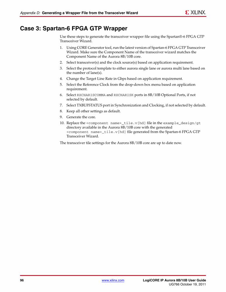
Appendix D: Generating a Wrapper File from the Transceiver Wizard
Case 3: Spartan-6 FPGA GTP WrapperUse these steps to generate the transceiver wrapper file using the Spartan®-6 FPGA GTP Transceiver Wizard.
1. Using CORE Generator tool, run the latest version of Spartan-6 FPGA GTP Transceiver Wizard. Make sure the Component Name of the transceiver wizard matches the Component Name of the Aurora 8B/10B core.
2. Select transceiver(s) and the clock source(s) based on application requirement.
3. Select the protocol template to either aurora single lane or aurora multi lane based on the number of lane(s).
4. Change the Target Line Rate in Gbps based on application requirement.
5. Select the Reference Clock from the drop-down box menu based on application requirement.
6. Select RXCHARISCOMMA and RXCHARISK ports in 8B/10B Optional Ports, if not selected by default.
7. Select TXBUFSTATUS port in Synchronization and Clocking, if not selected by default.
8. Keep all other settings as default.
9. Generate the core.
10. Replace the <component name>_tile.v[hd] file in the example_design/gt directory available in the Aurora 8B/10B core with the generated <component name>_tile.v[hd] file generated from the Spartan-6 FPGA GTP Transceiver Wizard.
The transceiver tile settings for the Aurora 8B/10B core are up to date now.
96 www.xilinx.com LogiCORE IP Aurora 8B/10B User GuideUG766 October 19, 2011

Appendix E
Aurora AXI4-Stream Migration Guide
IntroductionThis guide explains about migrating legacy (LocalLink based) Aurora cores to the AXI4-Stream Aurora core.
Pre-Requisites • ISE ® 13.3 software build containing the Aurora 8B/10B v7.1 core supporting the
AXI4-Stream protocol
• Familiarity with the Aurora directory structure
• Familiarity with running the Aurora example design
• Basic knowledge of the AXI4-Stream and LocalLink protocols
• Latest data sheet (DS797) and user guide (UG766) of the core with the AXI4-Stream updates
• Legacy data sheet (DS637) and data sheet (UG353) for reference
• Migration guide (this Appendix)
LimitationsThis section outlines the limitations of the Aurora 8B/10B core for AXI4-Stream support. The user has to take care of two limitations while interfacing the Aurora 8B/10B core with the AXI4-Stream compliant interface core:
1. The Aurora 8B/10B core supports only continuous aligned streams and continuous unaligned streams. The position bytes are valid only at the end of packet:
2. The AXI4-Stream protocol supports transfers with zero data at the end of packet, but the Aurora 8B/10B core expects at least one byte to be valid at the end of packet.
Overview of Major ChangesThe major change to the core is the addition of the AXI4-Stream interface:
• The user interface is modified from the legacy LocalLink (LL) to AXI4-Stream
• All AXI4-Stream signals are active High, whereas LocalLink signals are active Low
• The user interface in the example design and design top file is AXI4-Stream
• A new shim module is introduced in the AXI4-Stream Aurora core to convert AXI4-Stream signals to LL and LL back to AXI4-Stream
LogiCORE IP Aurora 8B/10B User Guide www.xilinx.com 97UG766 October 19, 2011

Appendix E: Aurora AXI4-Stream Migration Guide
• The AXI4-Stream to LL shim on the transmit converts all AXI4-Stream signals to LL
• The shim deals with active-High to active-Low conversions of signals between AXI4-Stream and LocalLink
• Generation of SOF_N and REM bits mapping is handled by the shim
• The LL to AXI4-Stream shim on the receive converts all LL signals to AXI4-Stream
• Each interface (PDU, UFC, and NFC) has a separate AXI4-Stream to LL and LL to AXI4-Stream shim instantiated from the design top file
• Frame generator and checker has respective LL to AXI4-Stream and AXI4-Stream to LL shim instantiated in the Aurora example design to interface with the generated AXI4-Stream design
Block DiagramFigure E-1 shows an example Aurora design using the legacy LocalLink interface. Figure E-2 shows an example Aurora design using the AXI-4 Stream interface.X-Ref Target - Figure E-1
Figure E-1: Legacy Aurora Example Design
98 www.xilinx.com LogiCORE IP Aurora 8B/10B User GuideUG766 October 19, 2011

Migration Steps
Migration Steps Generate an AXI4-Stream Aurora core from the CORE Generator™ tool using the ISE® tool v13.3 release.
Simulate the Core1. Run the vsim -do simulate_mti.do file from the /simulation/functional
directory.
2. ModelSim GUI launches and compiles the modules.
3. The wave_mti.do file loads automatically and populates AXI4-Stream signals.
4. Allow the simulation to run. This might take some time.
a. Initially lane up is asserted.
b. Channel up is then asserted and the data transfer begins.
c. Data transfer from all flow control interfaces now begins.
d. Frame checker continuously checks the received data and reports for any data mismatch.
5. A 'TEST PASS' or 'TEST FAIL' status is printed on the ModelSim console providing the status of the test.
Implement the Core1. Run ./implement.sh (for Linux) from the /implement directory.
2. The implement script compiles the core, runs through the ISE tool, and generates a bit file and netlist for the core.
Integrate to an Existing LocalLink-based Aurora Design 1. The Aurora core provides a light-weight 'shim' to interface to any existing LL based
interface. The shims are delivered along with the core from aurora_8b10b_v7_1 version of the core.
X-Ref Target - Figure E-2
Figure E-2: AXI4-Stream Aurora Example Design
LL to AXI4_S
AXI4-StreamAurora Design
AXI4-Stream Aurora Design Top
AXI4_S to LL
Existing LL based Design
LogiCORE IP Aurora 8B/10B User Guide www.xilinx.com 99UG766 October 19, 2011
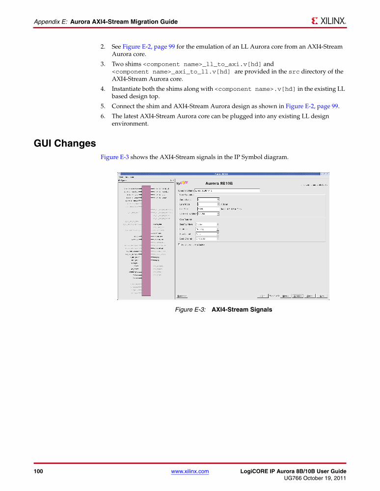
Appendix E: Aurora AXI4-Stream Migration Guide
2. See Figure E-2, page 99 for the emulation of an LL Aurora core from an AXI4-Stream Aurora core.
3. Two shims <component name>_ll_to_axi.v[hd] and <component name>_axi_to_ll.v[hd] are provided in the src directory of the AXI4-Stream Aurora core.
4. Instantiate both the shims along with <component name>.v[hd] in the existing LL based design top.
5. Connect the shim and AXI4-Stream Aurora design as shown in Figure E-2, page 99.
6. The latest AXI4-Stream Aurora core can be plugged into any existing LL design environment.
GUI ChangesFigure E-3 shows the AXI4-Stream signals in the IP Symbol diagram.X-Ref Target - Figure E-3
Figure E-3: AXI4-Stream Signals
100 www.xilinx.com LogiCORE IP Aurora 8B/10B User GuideUG766 October 19, 2011