Embed Size (px)
Citation preview
E3 237 Integrated Circuits for Wireless Communication
Lecture 2: RF CMOS Technology
Gaurab BanerjeeDepartment of Electrical Communication Engineering,
Indian Institute of Science, [email protected]

Outline
• CMOS scaling and technology parameters
• A “standard” RF-CMOS process
• Devices
• Resistors, Capacitors, Inductors and Transformers• Resistors, Capacitors, Inductors and Transformers

CMOS Constant Field Scaling
R. Dennard et al., IEEE J.S.S.C, 1974
• Scale vertical and horizontal dimensions by αααα
• Scale voltages (supply, threshold) by αααα
• Scale doping levels by αααα

Digital Analog
The Benefits of Scaling
Materials!
• Scaling has driven the digital revolution!
• Doesn’t work that well for analog, supply scaling hurts
• Performance improvement being driven by materials now.
• Higher fTs -> higher bandwidth for analog circuits
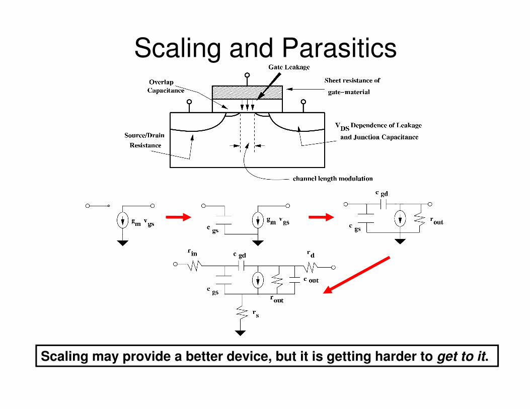
Scaling and Parasitics
Scaling may provide a better device, but it is getting harder to get to it.

CMOS Analog Building Blocks
Almost every kind of analog building block provided by CMOS!

Analog Building Blocks: Parasitics
• Parasitics can result in substantial deviation from ideal models
• Biggest Impact on RFICs -> Parasitics degrade fT and fmax
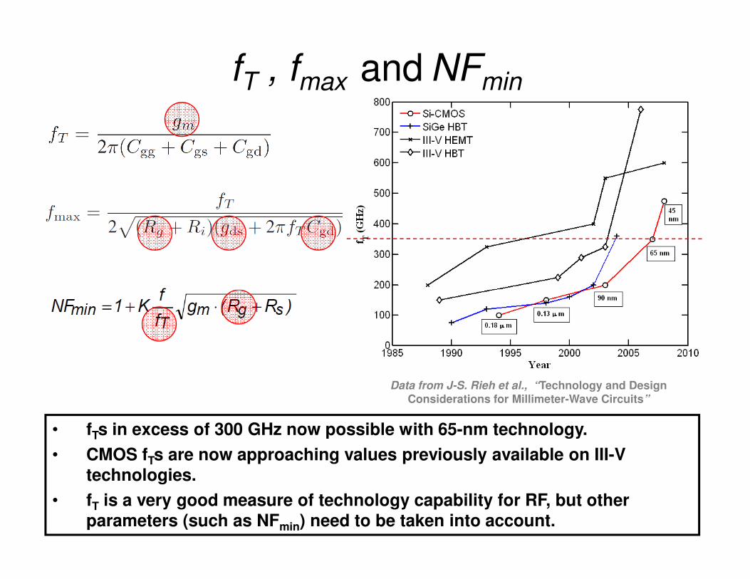
fT , fmax and NFmin
• fTs in excess of 300 GHz now possible with 65-nm technology.
• CMOS fTs are now approaching values previously available on III-V
technologies.
• fT is a very good measure of technology capability for RF, but other
parameters (such as NFmin) need to be taken into account.
Data from J-S. Rieh et al., “Technology and Design Considerations for Millimeter-Wave Circuits”
Outline
• CMOS scaling and technology parameters
• A “standard” RF-CMOS process
• Devices
• Resistors, Capacitors, Inductors and Transformers• Resistors, Capacitors, Inductors and Transformers
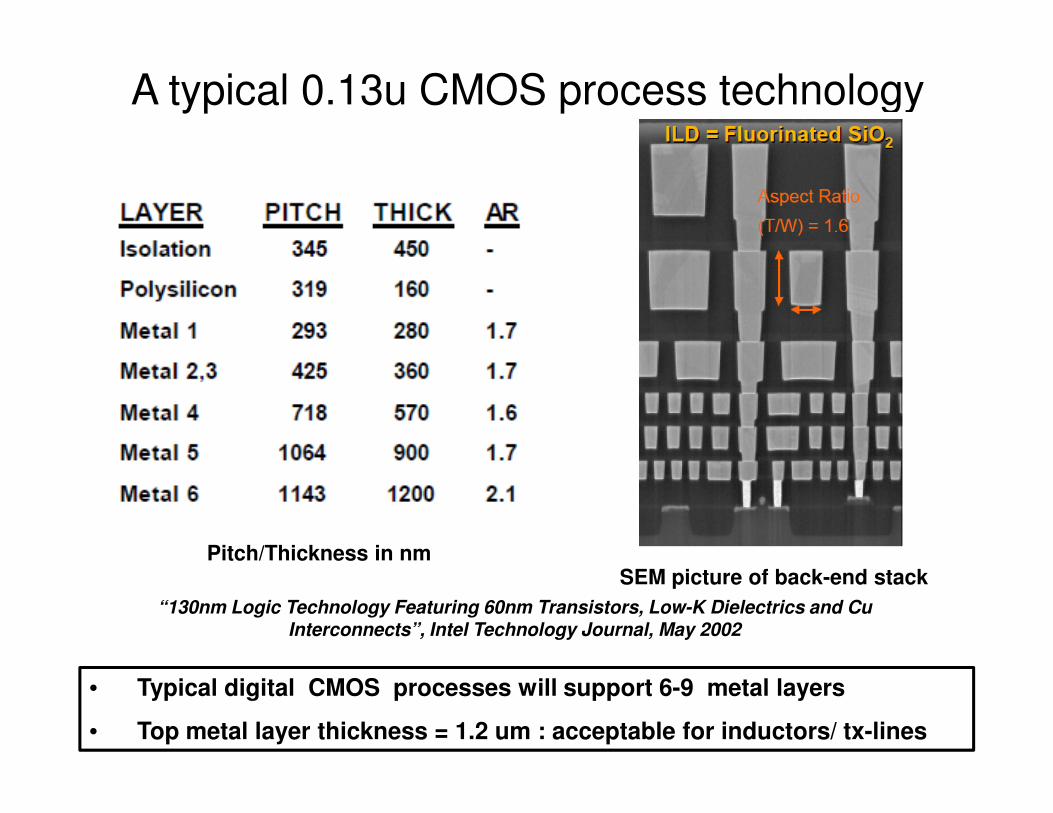
A typical 0.13u CMOS process technology
• Typical digital CMOS processes will support 6-9 metal layers
• Top metal layer thickness = 1.2 um : acceptable for inductors/ tx-lines
SEM picture of back-end stackPitch/Thickness in nm
“130nm Logic Technology Featuring 60nm Transistors, Low-K Dielectrics and Cu Interconnects”, Intel Technology Journal, May 2002

Intel’s 0.13-um CMOS : Active Devices
NMOS/PMOS combination with isolationDevice Cross-section
• The effective channel length is considerably smaller than the drawn length: In this case, 130 nm translates to 60-nm! – Important consequences for fT, fmax, linearity.
• This is a twin-well+STI process: 2 wells usually not attempted for cost reasons.
• Better NMOS/PMOS isolation may allow lower substrate doping, better inductors.
• Poly-Si is silicided to lower sheet resistance: common practice in modern CMOS – large poly resistors cannot be fabricated.
• May have additional doping/implants below the channel: usually for leakage control –important consequences for device linearity in RF
“130nm Logic Technology Featuring 60nm Transistors, Low-K Dielectrics and Cu Interconnects”, Intel Technology Journal, May 2002
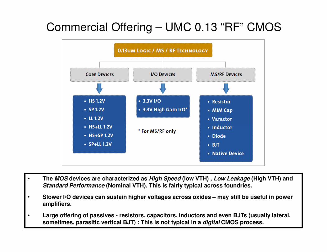
Commercial Offering – UMC 0.13 “RF” CMOS
• The MOS devices are characterized as High Speed (low VTH) , Low Leakage (High VTH) and Standard Performance (Nominal VTH). This is fairly typical across foundries.
• Slower I/O devices can sustain higher voltages across oxides – may still be useful in power amplifiers.
• Large offering of passives - resistors, capacitors, inductors and even BJTs (usually lateral, sometimes, parasitic vertical BJT) : This is not typical in a digital CMOS process.