Embed Size (px)
Citation preview

PRODUCTION DATA information is current as of publication date.Products conform to specifications per the terms of Texas Instrumentsstandard warranty. Production processing does not necessarily includetesting of all parameters.
PWM LOW-SIDE DRIVER (1.5A and 3A)for Solenoids, Coils, Valves, Heaters, and Lamps
FEATURES HIGH OUTPUT DRIVE: 1.5A and 3A Versions WIDE SUPPLY RANGE: +8V to +32V COMPLETE FUNCTION
Digitally Controlled InputPWM OutputAdjustable Internal Oscillator: 500Hz to 100kHzAdjustable Delay and Duty Cycle
FULLY PROTECTEDThermal and Current Limit Shutdown withStatus OK Indicator Flag
PACKAGES: SO-8 and PowerPAD™ SO-8
APPLICATIONS ELECTROMECHANICAL DRIVER:
Solenoids, Valves, Positioners, Actuators,Relays, Power Contactor Coils, Heaters, Lamps
HYDRAULIC AND PNEUMATICS SYSTEMS PART HANDLERS AND SORTERS CHEMICAL PROCESSING ENVIRONMENTAL MONITORING AND HVAC THERMOELECTRIC COOLERS DC MOTOR SPEED CONTROLS MEDICAL AND SCIENTIFIC ANALYZERS FUEL INJECTOR DRIVERS
DESCRIPTIONThe DRV103 is a low-side DMOS power switch employinga pulse-width modulated (PWM) output. Its rugged design isoptimized for driving electromechanical devices such asvalves, solenoids, relays, actuators, motors, and positioners.The DRV103 is also ideal for driving thermal devices suchas heaters, coolers, and lamps. PWM operation conservespower and reduces heat rise, resulting in higher reliability. Inaddition, adjustable PWM allows fine control of the powerdelivered to the load. DC-to-PWM output delay time andoscillator frequency are also externally adjustable.
The DRV103 can be set to provide a strong initial closure,automatically switching to a “soft” hold mode for powersavings. A resistor, analog voltage, or Digital-to-Analog(D/A) converter can control the duty cycle. An output OK flagindicates when thermal shutdown or over current occurs.
Two packages provide a choice of output current:1.5A (SO-8) or 3A (PowerPAD™ SO-8 with exposed metalheat sink).
The DRV103 is specified for –40°C to +85°C.
Delay Adj
CD RPWM
Input
On
Off
Thermal ShutdownOver Current
Status OKFlag
Load
+VS
OscillatorVREF
PWM
GND
OUT
FlybackDiodeDMOS
DMOS
ESD
Osc FreqAdj
Duty CycleAdj
RFREQ
Delay
DRV103
DRV103
SBVS029A – JUNE 2001
www.ti.com
Copyright © 2001, Texas Instruments Incorporated
Please be aware that an important notice concerning availability, standard warranty, and use in critical applications ofTexas Instruments semiconductor products and disclaimers thereto appears at the end of this data sheet.
PowerPAD is a trademark of Texas Instruments.
DRV103
DRV103

DRV1032SBVS029A
PACKAGE SPECIFIEDDRAWING TEMPERATURE PACKAGE ORDERING TRANSPORT
PRODUCT PACKAGE NUMBER RANGE MARKING NUMBER(1) MEDIA
DRV103U SO-8 182 –40°C to +85°C DRV103U DRV103U Rails" " " " " DRV103U/2K5 Tape and Reel
DRV103H PowerPAD™ SO-8 DDA –40°C to +85°C DRV103H DRV103H Rails" " " " " DRV103H/2K5 Tape and Reel
NOTES: (1) Models with a slash (/) are available only in Tape and Reel in the quantities indicated (e.g., /2K5 indicates 2500 devices per reel). Ordering 2500pieces of “DRV103U/2K5” will get a single 2500-piece Tape and Reel.
Supply Voltage, VS(2) ......................................................................... +40V
Input Voltage .................................................................. –0.2V to +5.5V(3)
PWM Adjust Input .......................................................... –0.2V to +5.5V(3)
Delay Adjust Input .......................................................... –0.2V to +5.5V(3)
Frequency Adjust Input .................................................. –0.2V to +5.5V(3)
Status OK Flag and OUT .................................................... –0.2V to VS(4)
Operating Temperature Range ...................................... –55°C to +125°CStorage Temperature Range ......................................... –65°C to +150°CJunction Temperature .................................................................... +150°CLead Temperature (soldering, 10s) ............................................... +300°C
NOTES: (1) Stresses above these ratings may cause permanent damage.Exposure to absolute maximum conditions for extended periods may de-grade device reliability. (2) See Bypassing section for discussion aboutoperating near maximum supply voltage. (3) Higher voltage may be appliedif current is limited to 2mA. (4) The Status OK Flag will internally current limitat about 10mA.
ABSOLUTE MAXIMUM RATINGS(1) ELECTROSTATICDISCHARGE SENSITIVITY
This integrated circuit can be damaged by ESD. Texas Instru-ments recommends that all integrated circuits be handled withappropriate precautions. Failure to observe proper handlingand installation procedures can cause damage.
ESD damage can range from subtle performance degradationto complete device failure. Precision integrated circuits maybe more susceptible to damage because very small parametricchanges could cause the device not to meet its publishedspecifications.
PACKAGE/ORDERING INFORMATION

DRV103 3SBVS029A
ELECTRICAL CHARACTERISTICSAt TC = +25°C, VS = +24V, Load = 100Ω, and 4.99kΩ “OK Flag” pullup to +5V, Delay Adj Capacitor = 100pF to Ground, Freq Adj Resistor = 205kΩ to Ground,Duty Cycle Adj Resistor = 137kΩ to Ground, unless otherwise noted.
DRV103U, H
PARAMETER CONDITIONS MIN TYP MAX UNITS
OUTPUTOutput Current(1) SO-8 Package (U) 1.5 A
PowerPAD™ SO-8 Package (H) 3 AOutput Saturation Voltage, Source IO = 1A +0.4 +0.6 V
IO = 0.1A +0.05 +0.07 VCurrent Limit(2), (10) 3 3.5 4.2 ALeakage Current DMOS Output Off, VO = +32V ±1 ±10 µA
DIGITAL CONTROL INPUT(3)
VCTR Low (output disabled) 0 +1.2 VVCTR High (output enabled) +2.2 +5.5 VICTR Low (output disabled) VCTR = 0V 0.01 1 µAICTR High (output enabled) VCTR = +5.5V 120 150 µAPropagation Delay On-to-Off and Off-to-On 1 µs
DELAY TO PWM(4) DC to PWM ModeDelay Equation(5) See Note (6) sDelay Time CD = 0.1µF 90 110 140 msMinimum Delay Time(7) CD = 0 18 µs
DUTY CYCLE ADJUSTDuty Cycle Range 10 to 90 %Duty Cycle Accuracy 50% Duty Cycle, 25kHz ±2 %
vs Supply Voltage 50% Duty Cycle, VS = VO = +8V to +32V ±2 %Nonlinearity(8) 10% to 90% Duty Cycle 1 % FSR
DYNAMIC RESPONSEOutput Voltage Rise Time VO = 10% to 90% of VS 0.2 2 µsOutput Voltage Fall Time VO = 90% to 10% of VS 0.2 2 µsOscillator Frequency Range External Adjust 0.5 to 100 kHzOscillator Frequency ROSC = 205kΩ 20 25 30 kHz
OK FLAGNormal Operation 20kΩ Pull-Up to +5V +4.5 5.0 VFault(90) Sinking 1mA +0.22 +0.4 VSink Current VOKFLAG = 0.4V 2 mAOver-Current Flag: Set 5 µs
THERMAL SHUTDOWNJunction Temperature
Shutdown +160 °CReset from Shutdown +140 °C
POWER SUPPLYSpecified Operating Voltage +24 VOperating Voltage Range +8 +32 VQuiescent Current IO = 0 0.4 0.8 mA
TEMPERATURE RANGESpecified Range –40 +85 °COperating Range –55 +125 °CStorage Range –65 +150 °CThermal Resistance, θJA
SO-8 (U) 1in2 0.5oz. Copper on PCB 150 °C/WPowerPAD™ SO-8 (H)(10) 1in2 0.5oz. Copper on PCB 68 °C/W
NOTES: (1) Output current is limited by internal current limit and by DRV103 power dissipation. (2) Output current resets to zero when current limit is reached.(3) Logic High enables output (normal operation). (4) Constant DC output to PWM (Pulse-Width Modulated) time. (5) Maximum delay is determined by an externalcapacitor. Pulling the Delay Adjust Pin LOW corresponds to an infinite (continuous) delay. (6) Delay to PWM ≈ CD • 106 (CD inF • 1.1). (7) Connecting the Delay Adjust Pin to +5V reduces delay time to less than 1µs. (8) VIN at pin 3 to percent of duty cycle at pin 6. (9) OK Flag LOW indicatesfault from over-temperature or over-current conditions. (10) PowerPAD™ SO-8 (H) package has highest continuous current (2A) because the chip operates at alower junction temperature when underside metal tab is connected to a heat sink or heat spreader. θJA = 68°C/W measured on DRV103 demo board;θJA = 58°C/W measured on JEDEC standard test board. H package θJC = 16.7°C/W.
DRV1034SBVS029A
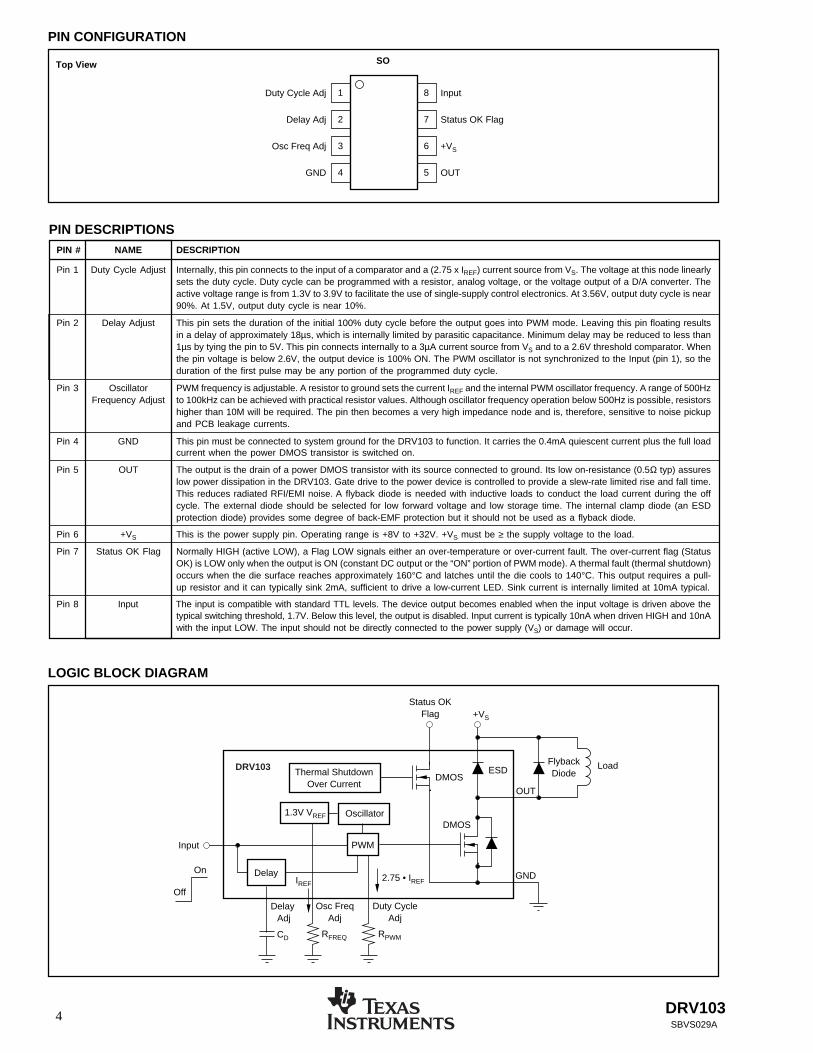
PIN # NAME DESCRIPTION
Pin 1 Duty Cycle Adjust Internally, this pin connects to the input of a comparator and a (2.75 x IREF) current source from VS. The voltage at this node linearlysets the duty cycle. Duty cycle can be programmed with a resistor, analog voltage, or the voltage output of a D/A converter. Theactive voltage range is from 1.3V to 3.9V to facilitate the use of single-supply control electronics. At 3.56V, output duty cycle is near90%. At 1.5V, output duty cycle is near 10%.
Pin 2 Delay Adjust This pin sets the duration of the initial 100% duty cycle before the output goes into PWM mode. Leaving this pin floating resultsin a delay of approximately 18µs, which is internally limited by parasitic capacitance. Minimum delay may be reduced to less than1µs by tying the pin to 5V. This pin connects internally to a 3µA current source from VS and to a 2.6V threshold comparator. Whenthe pin voltage is below 2.6V, the output device is 100% ON. The PWM oscillator is not synchronized to the Input (pin 1), so theduration of the first pulse may be any portion of the programmed duty cycle.
Pin 3 Oscillator PWM frequency is adjustable. A resistor to ground sets the current IREF and the internal PWM oscillator frequency. A range of 500HzFrequency Adjust to 100kHz can be achieved with practical resistor values. Although oscillator frequency operation below 500Hz is possible, resistors
higher than 10M will be required. The pin then becomes a very high impedance node and is, therefore, sensitive to noise pickupand PCB leakage currents.
Pin 4 GND This pin must be connected to system ground for the DRV103 to function. It carries the 0.4mA quiescent current plus the full loadcurrent when the power DMOS transistor is switched on.
Pin 5 OUT The output is the drain of a power DMOS transistor with its source connected to ground. Its low on-resistance (0.5Ω typ) assureslow power dissipation in the DRV103. Gate drive to the power device is controlled to provide a slew-rate limited rise and fall time.This reduces radiated RFI/EMI noise. A flyback diode is needed with inductive loads to conduct the load current during the offcycle. The external diode should be selected for low forward voltage and low storage time. The internal clamp diode (an ESDprotection diode) provides some degree of back-EMF protection but it should not be used as a flyback diode.
Pin 6 +VS This is the power supply pin. Operating range is +8V to +32V. +VS must be ≥ the supply voltage to the load.
Pin 7 Status OK Flag Normally HIGH (active LOW), a Flag LOW signals either an over-temperature or over-current fault. The over-current flag (StatusOK) is LOW only when the output is ON (constant DC output or the “ON” portion of PWM mode). A thermal fault (thermal shutdown)occurs when the die surface reaches approximately 160°C and latches until the die cools to 140°C. This output requires a pull-up resistor and it can typically sink 2mA, sufficient to drive a low-current LED. Sink current is internally limited at 10mA typical.
Pin 8 Input The input is compatible with standard TTL levels. The device output becomes enabled when the input voltage is driven above thetypical switching threshold, 1.7V. Below this level, the output is disabled. Input current is typically 10nA when driven HIGH and 10nAwith the input LOW. The input should not be directly connected to the power supply (VS) or damage will occur.
PIN DESCRIPTIONS
LOGIC BLOCK DIAGRAM
PIN CONFIGURATION
Top View
Duty Cycle Adj
Delay Adj
Osc Freq Adj
GND
Input
Status OK Flag
+VS
OUT
1
2
3
4
8
7
6
5
Delay Adj
CD RPWM
Input
On
Off
Thermal ShutdownOver Current
Status OKFlag
Load
+VS
Oscillator1.3V VREF
PWM
GND
OUT
FlybackDiodeDMOS
DMOS
ESD
Osc FreqAdj
Duty CycleAdj
2.75 • IREF
RFREQ
Delay
DRV103
IREF
SO

DRV103 5SBVS029A
TYPICAL CHARACTERISTICSAt TC = +25°C and VS = +24V, unless otherwise noted.
VOUT & IOUT WAVEFORMSSOLENOID LOAD
On
On
Off
IAVG
PWM Mode
Delay
Pull-In
3
2
1
0
IOU
T (A)
50
Time (ms)
1000
+VS
0
0
+VS
RL
VOUT & IOUT WAVEFORMSRESISTIVE LOAD
On
Off
IAVG
PWM Mode
Delay
3
2
1
0
IOU
T (A)
50
Time (ms)
1000
+VS
0
0
+VS
RL
CURRENT LIMIT SHUTDOWN WAVEFORMS
On
OK
OK OKOK
Off Off
FPWM = 25kHzDC = 50%Delay = 150µsReset Period = 1/FPWM
5
0
24
0
24
0
VIN (V
)V
OU
T (V)
50
Time (µs)
1000
VIN
VOUT
IO = 0A
IO = 3.5A
OK
StatusOK
FlagReset Period
5.0
4.5
4.0
3.5
3.0
2.5
2.0
1.5
1.0
0.5
0–10–60
I Q (
mA
)
40 90 140
QUIESCENT CURRENT vs JUNCTION TEMPERATURE
Temperature (°C)
32V
8V to 24V
40V (Absolute Maximum)
3.8
3.7
3.6
3.5
3.4
3.3–10–60
Cur
rent
(A
)
40 90 140
CURRENT LIMIT vs JUNCTION TEMPERATURE
Temperature (°C)
150
145
140
135
130
125
120
115
110
105
100–10–60
Del
ay (
ms)
40 90 140
DELAY vs JUNCTION TEMPERATURE
Temperature (°C)
CD = 0.1µF
+VS = 8V
+VS = 30V
+VS = 24V
+VS = 40V (Absolute Maximum)

DRV1036SBVS029A
TYPICAL CHARACTERISTICS (Cont.)At TC = +25°C and VS = +24V, unless otherwise noted.
50
40
30
20
10
0–10–60
Min
Del
ay (
µs)
40 90 140
MINIMUM DELAY vs JUNCTION TEMPERATURE
Temperature (°C)
CD = 0pF
25.5
25.3
25.1
24.9
24.7–10–60
Fre
quen
cy (
kHz)
40 90 140
OSCILLATOR FREQUENCY vs JUNCTION TEMPERATURE
Temperature (°C)
50.8
50.6
50.4
50.2
50.0
49.8
49.6
49.4
49.2–10–60
Dut
y C
ycle
(%
)
40 90 140
DUTY CYCLE vs JUNCTION TEMPERATURE
Temperature (°C)
RPWM = 137kΩ
1.6
1.4
1.2
1.0
0.8
0.6
0.4
0.2
0–10–60
VS
AT (
V)
40 90 140
VSAT vs JUNCTION TEMPERATURE
Temperature (°C)
IO = 3A
IO = 1.5A
IO = 0.1AIO = 0.5A
1.287
1.286
1.285
1.284
1.283
1.282
1.281
1.280
1.279
1.278
1.277
1.276–10–60
VF
RE
Q (
V)
40 90 140
VFREQ vs JUNCTION TEMPERATURE
Temperature (°C)
300
250
200
150
100
50
0
–504.54
Inpu
t Cur
rent
(µA
)
5 5.5 6
INPUT CURRENT vs INPUT VOLTAGE
Input Voltage (V)
DRV103 7SBVS029A
BASIC OPERATIONThe DRV103 is a low-side, DMOS power switch employinga Pulse-Width Modulated (PWM) output for driving electro-mechanical and thermal devices. Its design is optimized fortwo types of applications: a two-state driver (open/close) forloads such as solenoids and actuators; and a linear driver forvalves, positioners, heaters, and lamps. Its low 0.5Ω “ON”resistance, small size, adjustable delay to PWM mode, andadjustable duty cycle make it suitable for a wide range ofapplications.
Figure 1 shows the basic circuit connections to operate theDRV103. A 1µF (22µF when driving high current loads) orlarger tantalum bypass capacitor is recommended on thepower-supply pin.
Input (pin 8) is level-triggered and compatible with standardTTL levels. An input voltage between +2.2V and +5.5Vturns the device’s output ON, while a voltage of 0V to+1.2V shuts the DRV103’s output OFF. Input bias current istypically 1pA. Delay Adjust (pin 2) and Duty Cycle Adjust(pin 1) allow external adjustment of the PWM output signal.The Delay Adjust pin can be left floating for minimum delayto PWM mode (typically 18µs) or a capacitor can be used to
FIGURE 2. Typical DRV103 Timing Diagram, with CD = 3.9nF, OscFreq = 1kHz, and 75% Duty Cycle.
set a longer delay time. A resistor, analog voltage, or avoltage from a D/A converter can be used to control the dutycycle of the PWM output. The D/A converter must be ableto sink a current 2.75 • IREF (IREF = 1.3V/RFREQ).
Figure 2 illustrates a typical timing diagram with the DelayAdjust pin connected to a 3.9nF capacitor, the duty cycle setto 75%, and oscillator frequency set to 1kHz. See the “DelayAdjust” and “Duty Cycle Adjust” text for equations andfurther explanation. Ground (pin 4) must be connected tosystem ground for the DRV103 to function. This serves asthe load current path to ground, as well as the DRV103signal ground. The load (relay, solenoid, valve, etc.) shouldbe connected between the supply (pin 5) and output (pin 6).For an inductive load, an external “flyback” diode is re-quired, as shown in Figure 1. The diode serves to maintaincontinuous current flow in the inductive load during OFFperiods of PWM operation. For remotely located loads, theexternal diode is ideally located next to the DRV103. Theinternal ESD clamp diode between the output and supply isnot intended to be used as a “flyback diode.” The Status OKFlag (pin 7) provides fault status for over-current andthermal shutdown conditions. This pin is active LOW withoutput voltage of typically +0.3V during a fault condition.
Delay Adj
CD RPWM
TTL IN
Relay
+VS
GND
OUT
+VSStatusOK
3AFlybackDiode(1)
+8V to +32V
Osc FreqAdj
Duty CycleAdj
RFREQ
DRV103
1µF
4132
85
67
RLED
LEDOK = LED “on”
2mA
+
NOTE: (1) Motorola MSRS1100T3 (1A, 100V)
Motorola MBRS360T3 (3A, 60V)
or
Microsemi SK34MS (3A, 40V)
FIGURE 1. DRV103 Basic Circuit Connections.
TOFF
TON
ON
OFFOFFPeriod = = TON + TOFF
1FREQ
Duty Cycle = TON
TON + TOFF
Delay Time
+VS
VO (V)
0
+VS/RL
IO (A)
0
TTL HIGH
Input (V)
TTL LOW
0 1 2 3 4Time (ms)
5 6 7 8 9

DRV1038SBVS029A
The internal Delay Adjust circuitry is composed of a 3µAcurrent source and a 2.6V comparator, as shown in Figure 3.Thus, when the pin voltage is less than 2.6V, the outputdevice is 100% ON (DC output mode).
OSCILLATOR FREQUENCY ADJUST
The DRV103 PWM output frequency can be easily pro-grammed over a wide range by connecting a resistor (RFREQ)between the Osc Freq Adj pin (pin 3) and ground. A range of500Hz to 100kHz can be achieved with practical resistorvalues, as shown in Table II. Refer to “PWM Frequency vsRFREQ” typical performance curve shown in Figure 4 foradditional information. Although oscillator frequency opera-tion below 500Hz is possible, resistors higher than 10M willbe required. The pin becomes a very high impedance node andis, therefore, sensitive to noise pickup and PCB leakagecurrents if very high resistor values are used. Refer to Figure3 for a simplified circuit of the frequency adjust input.
APPLICATIONS INFORMATIONPOWER SUPPLY
The DRV103 operates from a single +8V to +32V supplywith excellent performance. Most behavior remains un-changed throughout the full operating voltage range. Param-eters that vary significantly with operating voltage are shownin the Typical Performance Curves. The DRV103 supplyvoltage should be ≥ the supply voltage on the load.
ADJUSTABLE DELAY TIME (INITIAL 100% DUTY CYCLE)
A unique feature of the DRV103 is its ability to provide aninitial constant DC output (100% duty cycle) and thenswitch to PWM mode output to save power. This function isparticularly useful when driving solenoids that have a muchhigher pull-in current requirement than continuous holdrequirement.
The duration of this constant DC output (before PWMoutput begins) can be externally controlled by a capacitorconnected from Delay Adjust (pin 2) to ground according tothe following equation:
Delay Time ≈ CD • 106
(time in seconds, CD in Farads • 1.1)
Leaving the Delay Adjust pin open results in a constantoutput time of approximately 18µs. The duration of thisinitial output can be reduced to less than 1µs by connectingthe pin to 5V. Table I provides examples of delay times(constant output before PWM mode) achieved with selectedcapacitor values.
INITIAL CONSTANTOUTPUT DURATION CD
1µs Pin 2 Tied to +5V18µs Pin 2 Open110µs 100pF1.1ms 1nF11ms 10nF110ms 100nF1.1s 1µF11s 10µF
TABLE I. Delay Adjust Times.
FIGURE 3. Simplified Delay Adjust and Frequency Adjust Inputs.
3µA
CD
RFREQ
VFREQ
IREF
+VS
VREF
Reset
+2.6V
+1.3V
Input
1000M
100M
10M
1M
100k
10k
1k100 1k10
RF
RE
Q (
Ω)
10k 100k 1M
PWM FREQUENCY vs RFREQ
Frequency (Hz)
FIGURE 4. Using a Resistor to Program Oscillator Frequency.RFREQ (kΩ) = 6808417/F(1.0288)
OSCILLATOR FREQUENCY RFREQ (nearest 1% values)(Hz) (Ω)
100k 47.5k50k 100k25k 205k10k 523k5k 1.07M
500 11.3M
TABLE II. Oscillator Frequency Resistance.

DRV103 9SBVS029A
A 100pF capacitor in parallel with RPWM is recommendedwhen switching a high load current to maintain a cleanoutput switching waveform, as shown in Figure 6.
The DRV103’s adjustable PWM output frequency allows itto be optimized for driving virtually any type of load.
ADJUSTABLE DUTY CYCLE (PWM Mode)
The DRV103’s externally adjustable duty cycle provides anaccurate means of controlling power delivered to a load.Duty cycle can be set over a range of at least 10% to 90%with an external resistor, analog voltage, or the voltageoutput of a D/A converter. A low duty cycle results inreduced power dissipation in the load. This keeps the DRV103and the load cooler, resulting in increased reliability for bothdevices.
Resistor Controlled Duty Cycle
Duty cycle is easily programmed by connecting a resistor(RPWM) between the Duty Cycle Adjust pin (pin 1) andground. High resistor values correspond to high duty cycles.Table III provides resistor values for typical duty cycles.Resistor values for additional duty cycles can be obtainedfrom Figure 5. For reference purposes, the equation forcalculating RPWM is included in Figure 5.
DUTY CYCLE RPWM (Nearest 1% Values)
(%) 5kHz 25kHz 100kHz
5 374k 75k 16.9k10 402k 80.6k 19.1k20 475k 95.3k 22.6k30 549k 110k 26.1k40 619k 124k 29.4k50 681k 137k 33.2k60 750k 150k 37.4k70 825k 165k 40.2k80 887k 182k 44.2k90 953k 196k 47.5k95 1M 200k 49.9k
TABLE III. Duty Cycle Adjust Resistance.
FIGURE 5. Using a Resistor to Program Duty Cycle.At 25kHz: RPWM (kΩ) = 67.46 + 1.41 • %DC.
1M
100k
10k20 400
RP
WM
(Ω
)
60 80 100
DUTY CYCLE vs RPWM
Duty Cycle (%)
5kHz
25kHz
100kHz
RPWMonly onPin 1
With100pF inParallel withRPWM
Time (10µs)
FIGURE 6. Output Waveform at High Load Current.
100
90
80
70
60
50
40
30
20
10
021
Dut
y C
ycle
(%
)
2
1.5
1
0.5
0
–0.5
–1
–1.5
–2
Dut
y C
ycle
Err
or (
%)
3 4
DUTY CYCLE AND DUTY CYCLE ERRORvs VOLTAGE
VPWM (V)
FIGURE 7. Using a Voltage to Program Duty Cycle.At VS = 24V and F = 25kHz: VPWM = 1.25 +0.026 • %DC.
Voltage Controlled Duty Cycle
Duty cycle can also be programmed by an analog voltage,VPWM. With VPWM ≈ 3.56V, duty cycle is about 90%.Decreasing this voltage results in decreased duty cycles.Table IV provides VPWM values for typical duty cycles. The“Duty Cycle vs Voltage” typical performance curve foradditional duty cycles is shown in Figure 7.
DUTY CYLE VPWM(%) (V)
5 1.34410 1.51820 1.76340 2.28360 2.78880 3.31190 3.56195 3.705
TABLE IV. Duty Cycle Adjust Voltage.

DRV10310SBVS029A
The Duty Cycle Adjust pin is internally driven by anoscillator frequency dependent current source and connectsto the input of a comparator as shown in Figure 8. TheDRV103’s PWM adjustment is inherently monotonic. Thatis, a decreased voltage (or resistor value) always producesan increased duty cycle.
DRV103
Thermal ShutdownOver Current
PWM
4
5
7
OUT
5kΩPull-Up
+5V
OK
TTL or HCT
FIGURE 9. Non-Latching Fault Monitoring Circuit.
FIGURE 10. Latching Fault Monitoring Circuit.
7
5kΩ
+5V
OK
(LED)HLMP-Q156
7
DRV103
Thermal ShutdownOver Current
4
5OUT
PWM
FIGURE 11. LED to Indicate Fault Condition.
7
20kΩ
+5V
Q
Q
CLR
OK
OK
OK Reset
J
CLK
GND K
VS
74XX76A
(1)
NOTE: (1) Small capacitor (10pF) may be required in noisy environments.
DRV103
Thermal ShutdownOver Current
4
5OUT
PWM
OK
2.75 • IREF
RPWM
+VS
OSC3.9V
1.3V
FIGURE 8. Simplified Duty Cycle Adjust Input.
STATUS FLAG
The OK Flag (pin 7) provides a fault indication for over-current and thermal shutdown conditions. During a faultcondition, the Status OK Flag output is driven LOW (pinvoltage typically drops to 0.3V). A pull-up resistor, asshown in Figure 9, is required to interface with standardlogic. Figure 9 also gives an example of a non-latching faultmonitoring circuit, while Figure 10 provides a latchingversion. The OK Flag pin can sink up to 10mA, sufficientto drive external logic circuitry, a reed relay, or an LED, asshown in Figure 11, to indicate when a fault has occurred.In addition, the OK Flag pin can be used to turn off otherDRV103s in a system for chain fault protection.
Over Current Fault
An over-current fault occurs when the PWM peak outputcurrent is greater than approximately 3.75A. The OK flag isnot latched. Since current during PWM mode is switched onand off, the OK flag output will be modulated with PWMtiming (see OK flag waveforms in the Typical PerformanceCurves).
Avoid adding capacitance to pin 6 (Out) as it may causemomentary current limiting.
Over-Temperature Fault
A thermal fault occurs when the die reaches approximately160°C, producing a similar effect as pulling the input low.Internal shutdown circuitry disables the output. The OKFlag is latched in the LOW state (fault condition) until thedie has cooled to approximately 140°C.

DRV103 11SBVS029A
PACKAGE MOUNTING
Figure 12 provides recommended PCB layouts for both theSO-8 (U) and the PowerPAD™ SO-8 (H) packages. Al-though the metal pad of the PowerPAD™ SO-8 (H) packageis electrically connected to ground (pin 4), no current shouldflow in this pad. Do NOT use the exposed metal pad as apower ground connection or erratic operation will result. Forlowest overall thermal resistance, it is best to solder thePowerPAD™ directly to a circuit board, as illustrated inFigure 13. Increasing the “heat sink” copper area improvesheat dissipation. Figure 14 shows typical junction-to-ambi-ent thermal resistance as a function of the PC board copperarea.
POWER DISSIPATION
DRV103 power dissipation depends on power supply, signal,and load conditions. Power dissipation (PD) is equal to theproduct of output current times the voltage across the conduct-ing DMOS transistor times the duty cycle. Using the lowestpossible duty cycle necessary to assure the required hold forcecan minimize power dissipation in both the load and in theDRV103. For low current, the output DMOS transistor on-resistance is 0.5Ω, increasing to 0.6Ω at high output current.
At very high oscillator frequencies, the energy in the DRV103’slinear rise and fall times can become significant and cause anincrease in PD.
Application Bulletin SBFA002 at www.ti.com, explains how tocalculate or measure power dissipation with unusual signalsand loads.
THERMAL PROTECTION
Power dissipated in the DRV103 will cause its internal junctiontemperature to rise. The DRV103 has an on-chip thermalshutdown circuitry that protects the IC from damage. Thethermal protection circuitry disables the output when the junc-tion temperature reaches approximately +160°C, allowing thedevice to cool. When the junction temperature cools to approxi-mately +140°C, the output circuitry is again enabled. Depend-ing on load and signal conditions, the thermal protection circuitmay cycle on and off. This limits the dissipation of the driverbut may have an undesirable effect on the load.
Any tendency to activate the thermal protection circuit indi-cates excessive power dissipation or an inadequate heat sink.For reliable operation, junction temperature should be limitedto +125°C, maximum. To estimate the margin of safety in acomplete design (including heat sink), increase the ambienttemperature until the thermal protection is triggered. Useworst-case load and signal conditions. For good reliability,thermal protection should trigger more than 40°C above themaximum expected ambient condition of your application.This produces a junction temperature of 125°C at the maxi-mum expected ambient condition.
THERMAL RESISTANCE vs CIRCUIT BOARD COPPER AREA
80
70
60
50
40
30
The
rmal
Res
ista
nce,
θJA
(°C
/W)
0 1 2 3 4 5
Copper Area (inches2)
DRV103 (H)Power PAD
Surface-Mount Package1oz. copper
FIGURE 12. Recommended PCB Layout.
FIGURE 13. PowerPAD Heat Transfer.
FIGURE 14. Heat Sink Thermal Resistance vs Circuit BoardCopper Area.
150 (ref)
C - C215 (ref)
95 x 95DRV103(H)
Package
60 (ref)
50 nom 1822
273277
153158
Copper Traces
Signal Trace
Copper Pad
Thermal Vias
DRV103 Die
Pad-to-BoardSolder

DRV10312SBVS029A
The internal protection circuitry of the DRV103 was designedto protect against overload conditions. It was not intended toreplace proper heat sinking. Continuously running theDRV103 into thermal shutdown will degrade reliability.
HEAT SINKING
Most applications will not require a heat sink to assure thatthe maximum operating junction temperature (125°C) is notexceeded. However, junction temperature should be kept aslow as possible for increased reliability. Junction tempera-ture can be determined according to the equation:
TJ = TA + PDθJA (1)
where, θJA = θJC + θCH + θHA (2)
TJ = Junction Temperature (°C)
TA = Ambient Temperature (°C)
PD = Power Dissipated (W)θJC = Junction-to-Case Thermal Resistance (°C/W)
θCH = Case-to-Heat Sink Thermal Resistance (°C/W)
θHA = Heat Sink-to-Ambient Thermal Resistance (°C/W)θJA = Junction-to-Air Thermal Resistance (°C/W)
Using a heat sink significantly increases the maximumallowable power dissipation at a given ambient temperature.
The answer to the question of selecting a heat sink lies indetermining the power dissipated by the DRV103. For DCoutput into a purely resistive load, power dissipation is simplythe load current times the voltage developed across theconducting output transistor times the duty cycle. Other loadsare not as simple. For further insight on calculating powerdissipation, refer to Application Bulletin SBFA002 atwww.ti.com. Once power dissipation for an application isknown, the proper heat sink can be selected.
Heat Sink Selection Example
A PowerPAD™ SO-8 (H) package is dissipating 2W. Themaximum expected ambient temperature is 35°C. Find theproper heat sink to keep the junction temperature below125°C.
Combining Equations 1 and 2 gives:
TJ = TA + PD(θJC + θCH + θHA) (3)
TJ, TA, and PD are given. θJC is provided in the specificationtable, 16.7°C/W. θCH depends on heat sink size, area, andmaterial used. A semiconductor’s package type and mount-ing can also affect θCH. A typical θCH for a soldered-in-placePowerPAD™ SO-8 (H) package is 2°C/W. Now we cansolve for θHA:
θ θ θ
θ
θ
HAJ A
DJC CH
HA
HA
T T
P
C C
WC W C W
C W
= +( )
= ° ° ° + °( )
= °
––
–– . / /
. /
125 35
216 7 2
26 3
(4)
To maintain junction temperature below 125°C, the heatsink selected must have a θHA less than 26.3°C/W. In otherwords, the heat sink temperature rise above ambient must beless than 52.6°C (26.3°C/W • 2W).
Another variable to consider is natural convection versusforced convection air flow. Forced-air cooling by a small fancan lower θCA (θCH + θHA) dramatically.
As mentioned earlier, once a heat sink has been selected, thecomplete design should be tested under worst-case load andsignal conditions to ensure proper thermal protection.
RFI/ EMI
Any switching system can generate noise and interferenceby radiation or conduction. The DRV103 is designed withcontrolled slew rate current switching to reduce these ef-fects. By slowing the rise and fall times of the output to0.3µs, much lower switching noise is generated.
Radiation from the DRV103-to-load wiring (the “antenna”effect) can be minimized by using “twisted pair” cable or byshielding. Good PCB ground planes are recommended forlow noise and good heat dissipation. Refer to Bypassingsection for notes on placement of the flyback diode.
BYPASSING
A 1µF tantalum bypass capacitor is adequate for uniformduty cycle control when switching loads of less than 0.5amps. Larger bypass capacitors are required when switchinghigh current loads. A 22µF tantalum capacitor is recom-mended for heavy-duty (3A) applications. It may also bedesirable to run the DRV103 and the load on separate powersupplies at high load currents. Near the absolute maximumsupply voltage of 40V, bypassing is especially critical. In theevent of a current overload, the DRV103 current limitresponds in microseconds, dropping the load current to zero.With inadequate bypass, energy stored in the supply lineinductance can lift the supply sufficiently to exceed voltagebreakdown with catastrophic results.
Place the flyback diode at the DRV103 end when drivinglong (inductive) cables to a remotely located load. Thisminimizes RFI / EMI and helps protect the output DMOStransistor from breakdown caused by dI/dt transients. Fastrectifier diodes such as epitaxial silicon or Schottky typesare recommended as flyback diodes.

DRV103 13SBVS029A
Delay Adj
0.22µF 205kΩ
+12V
GND
OUTInput
+VSOK
MicrosemiSK34MS3A 40V Schottky
Duty CycleAdj
FreqAdj
137kΩ
47µFTantalum
DRV103
22µF
4
312
81.7V5
671MΩ
316kΩ
"Fault"HLMP-0156 +
+CT
CT (µF)
4722104.72.2
TON (s)
10521
0.5
5.6kΩ
Relay
Delay Adj
Duty Cycle Adj
Freq Adj
0.1µF 205kΩ
GND
OUT
Input
+VS
137kΩ
DRV103
22µF
4
312
8
5
6
+
24kΩ
3.9kΩ
+28V
Housing
Relay
FIGURE 15. Time Delay Relay Driver.
FIGURE 16. Remotely Operated Solenoid Valve or Relay.
APPLICATIONS CIRCUITS

DRV10314SBVS029A
Delay Adj
CD 10MΩ
+12V
GND
OUTInput
+VS
Duty CycleAdj
FreqAdj
RPWM
3kΩ
DRV103
22µF
4
312
85
6
+
LOAD
(1)
TTLIN
High = Load ON
Low = Load OFF
NOTE: (1) Flyback diode required for inductive loads: IXYS DSE160-06A.
F ~ 500Hz
IRF4905
12V70A
TTL IN
LinearValveActuator
OUT5
8
2 1 3NC
67
4
+VSStatusOK
+8V to +32V
DRV103
22µF
MicrosemiSK34MS3A 40VSchottky
HLMP-Q156 “Fault”
2mA
Delay Adj
205kΩ
GNDDuty CycleAdj
FreqAdj
High = ONLow = OFF
+
1.3V ≅ 5% Duty Cycle3.7V ≅ 95% Duty Cycle
DACDATA
FIGURE 17. High Power High Side Driver.
FIGURE 18. Linear Valve Driver.
PACKAGING INFORMATION
Orderable Device Status (1) PackageType
PackageDrawing
Pins PackageQty
Eco Plan (2) Lead/Ball Finish MSL Peak Temp (3)
DRV103H NRND SOPower PAD
DDA 8 75 Green (RoHS &no Sb/Br)
CU SN Level-1-260C-UNLIM
DRV103H/2K5 NRND SOPower PAD
DDA 8 2500 Green (RoHS &no Sb/Br)
CU SN Level-1-260C-UNLIM
DRV103H/2K5G3 NRND SOPower PAD
DDA 8 2500 Green (RoHS &no Sb/Br)
CU SN Level-1-260C-UNLIM
DRV103HG3 NRND SOPower PAD
DDA 8 75 Green (RoHS &no Sb/Br)
CU SN Level-1-260C-UNLIM
DRV103U NRND SOIC D 8 75 Green (RoHS &no Sb/Br)
CU NIPDAU Level-2-260C-1 YEAR
DRV103U/2K5 NRND SOIC D 8 2500 Green (RoHS &no Sb/Br)
CU NIPDAU Level-2-260C-1 YEAR
DRV103U/2K5G4 NRND SOIC D 8 2500 Green (RoHS &no Sb/Br)
CU NIPDAU Level-2-260C-1 YEAR
DRV103UG4 NRND SOIC D 8 75 Green (RoHS &no Sb/Br)
CU NIPDAU Level-2-260C-1 YEAR
(1) The marketing status values are defined as follows:ACTIVE: Product device recommended for new designs.LIFEBUY: TI has announced that the device will be discontinued, and a lifetime-buy period is in effect.NRND: Not recommended for new designs. Device is in production to support existing customers, but TI does not recommend using this part ina new design.PREVIEW: Device has been announced but is not in production. Samples may or may not be available.OBSOLETE: TI has discontinued the production of the device.
(2) Eco Plan - The planned eco-friendly classification: Pb-Free (RoHS), Pb-Free (RoHS Exempt), or Green (RoHS & no Sb/Br) - please checkhttp://www.ti.com/productcontent for the latest availability information and additional product content details.TBD: The Pb-Free/Green conversion plan has not been defined.Pb-Free (RoHS): TI's terms "Lead-Free" or "Pb-Free" mean semiconductor products that are compatible with the current RoHS requirementsfor all 6 substances, including the requirement that lead not exceed 0.1% by weight in homogeneous materials. Where designed to be solderedat high temperatures, TI Pb-Free products are suitable for use in specified lead-free processes.Pb-Free (RoHS Exempt): This component has a RoHS exemption for either 1) lead-based flip-chip solder bumps used between the die andpackage, or 2) lead-based die adhesive used between the die and leadframe. The component is otherwise considered Pb-Free (RoHScompatible) as defined above.Green (RoHS & no Sb/Br): TI defines "Green" to mean Pb-Free (RoHS compatible), and free of Bromine (Br) and Antimony (Sb) based flameretardants (Br or Sb do not exceed 0.1% by weight in homogeneous material)
(3) MSL, Peak Temp. -- The Moisture Sensitivity Level rating according to the JEDEC industry standard classifications, and peak soldertemperature.
Important Information and Disclaimer:The information provided on this page represents TI's knowledge and belief as of the date that it isprovided. TI bases its knowledge and belief on information provided by third parties, and makes no representation or warranty as to theaccuracy of such information. Efforts are underway to better integrate information from third parties. TI has taken and continues to takereasonable steps to provide representative and accurate information but may not have conducted destructive testing or chemical analysis onincoming materials and chemicals. TI and TI suppliers consider certain information to be proprietary, and thus CAS numbers and other limitedinformation may not be available for release.
In no event shall TI's liability arising out of such information exceed the total purchase price of the TI part(s) at issue in this document sold by TIto Customer on an annual basis.
PACKAGE OPTION ADDENDUM
www.ti.com 1-Feb-2010
Addendum-Page 1

TAPE AND REEL INFORMATION
*All dimensions are nominal
Device PackageType
PackageDrawing
Pins SPQ ReelDiameter
(mm)
ReelWidth
W1 (mm)
A0 (mm) B0 (mm) K0 (mm) P1(mm)
W(mm)
Pin1Quadrant
DRV103H/2K5 SOPower PAD
DDA 8 2500 330.0 12.4 6.4 5.2 2.1 8.0 12.0 Q1
DRV103U/2K5 SOIC D 8 2500 330.0 12.4 6.4 5.2 2.1 8.0 12.0 Q1
PACKAGE MATERIALS INFORMATION
www.ti.com 14-Mar-2008
Pack Materials-Page 1

*All dimensions are nominal
Device Package Type Package Drawing Pins SPQ Length (mm) Width (mm) Height (mm)
DRV103H/2K5 SO PowerPAD DDA 8 2500 346.0 346.0 29.0
DRV103U/2K5 SOIC D 8 2500 346.0 346.0 29.0
PACKAGE MATERIALS INFORMATION
www.ti.com 14-Mar-2008
Pack Materials-Page 2


IMPORTANT NOTICE
Texas Instruments Incorporated and its subsidiaries (TI) reserve the right to make corrections, modifications, enhancements, improvements,and other changes to its products and services at any time and to discontinue any product or service without notice. Customers shouldobtain the latest relevant information before placing orders and should verify that such information is current and complete. All products aresold subject to TI’s terms and conditions of sale supplied at the time of order acknowledgment.
TI warrants performance of its hardware products to the specifications applicable at the time of sale in accordance with TI’s standardwarranty. Testing and other quality control techniques are used to the extent TI deems necessary to support this warranty. Except wheremandated by government requirements, testing of all parameters of each product is not necessarily performed.
TI assumes no liability for applications assistance or customer product design. Customers are responsible for their products andapplications using TI components. To minimize the risks associated with customer products and applications, customers should provideadequate design and operating safeguards.
TI does not warrant or represent that any license, either express or implied, is granted under any TI patent right, copyright, mask work right,or other TI intellectual property right relating to any combination, machine, or process in which TI products or services are used. Informationpublished by TI regarding third-party products or services does not constitute a license from TI to use such products or services or awarranty or endorsement thereof. Use of such information may require a license from a third party under the patents or other intellectualproperty of the third party, or a license from TI under the patents or other intellectual property of TI.
Reproduction of TI information in TI data books or data sheets is permissible only if reproduction is without alteration and is accompaniedby all associated warranties, conditions, limitations, and notices. Reproduction of this information with alteration is an unfair and deceptivebusiness practice. TI is not responsible or liable for such altered documentation. Information of third parties may be subject to additionalrestrictions.
Resale of TI products or services with statements different from or beyond the parameters stated by TI for that product or service voids allexpress and any implied warranties for the associated TI product or service and is an unfair and deceptive business practice. TI is notresponsible or liable for any such statements.
TI products are not authorized for use in safety-critical applications (such as life support) where a failure of the TI product would reasonablybe expected to cause severe personal injury or death, unless officers of the parties have executed an agreement specifically governingsuch use. Buyers represent that they have all necessary expertise in the safety and regulatory ramifications of their applications, andacknowledge and agree that they are solely responsible for all legal, regulatory and safety-related requirements concerning their productsand any use of TI products in such safety-critical applications, notwithstanding any applications-related information or support that may beprovided by TI. Further, Buyers must fully indemnify TI and its representatives against any damages arising out of the use of TI products insuch safety-critical applications.
TI products are neither designed nor intended for use in military/aerospace applications or environments unless the TI products arespecifically designated by TI as military-grade or "enhanced plastic." Only products designated by TI as military-grade meet militaryspecifications. Buyers acknowledge and agree that any such use of TI products which TI has not designated as military-grade is solely atthe Buyer's risk, and that they are solely responsible for compliance with all legal and regulatory requirements in connection with such use.
TI products are neither designed nor intended for use in automotive applications or environments unless the specific TI products aredesignated by TI as compliant with ISO/TS 16949 requirements. Buyers acknowledge and agree that, if they use any non-designatedproducts in automotive applications, TI will not be responsible for any failure to meet such requirements.
Following are URLs where you can obtain information on other Texas Instruments products and application solutions:
Products Applications
Amplifiers amplifier.ti.com Audio www.ti.com/audio
Data Converters dataconverter.ti.com Automotive www.ti.com/automotive
DLP® Products www.dlp.com Communications and www.ti.com/communicationsTelecom
DSP dsp.ti.com Computers and www.ti.com/computersPeripherals
Clocks and Timers www.ti.com/clocks Consumer Electronics www.ti.com/consumer-apps
Interface interface.ti.com Energy www.ti.com/energy
Logic logic.ti.com Industrial www.ti.com/industrial
Power Mgmt power.ti.com Medical www.ti.com/medical
Microcontrollers microcontroller.ti.com Security www.ti.com/security
RFID www.ti-rfid.com Space, Avionics & www.ti.com/space-avionics-defenseDefense
RF/IF and ZigBee® Solutions www.ti.com/lprf Video and Imaging www.ti.com/video
Wireless www.ti.com/wireless-apps
Mailing Address: Texas Instruments, Post Office Box 655303, Dallas, Texas 75265Copyright © 2010, Texas Instruments Incorporated