Embed Size (px)
Citation preview

Digital VLSI Design
Design of Very Large Scale Integrated Digital circuits
using CAD tools
http://uhaweb.hartford.edu/ilumokanw

SyllabusUniversity of Hartford – College of Engineering
Electrical Engineering DepartmentECE565 Digital VLSI Design
Fall 2005Professor: Dr. Abby Ilumoka, Room UT 235, Ph: (860) - 768 – 5231 Email: [email protected] Website: http://uhaweb.hartford.edu/ilumokanwClass Time: Tue Thu, 4.15-5.30pmOffice Hrs: : Wed 2-3.30pm, Tues, Thur 1.30pm – 2.30pm (other consultation by appointment)Credit Hours 3 Lecture Hours 1.75hr/w Laboratory Hours 0.75hr/wkPrerequisites/Co-requisites Digital System Logic(EE231), Digital Laboratory(EE232), Electronics Circuits
(EE362), Electronics Lab II (EE364), Senior or graduate standingTextbook Digital Integrated Circuit Design by Martin, Oxford PublishingReferences CMOS Digital and Analog Circuit Design by John Uyemura, Oxford PublishingSoftware Tanner VLSI Design Suite: LEDIT Pro Full Custom Layout Editor,
TSPICE Pro Circuit Simulator, UPLib, CMOS Lib, SEDIT Schematic Editor, LVS Netlist Comparator

Syllabus (contd)
Bulletin Description Techniques for CMOS digital integrated circuit design at circuit,
subsystem and system levels. CAD tools for design from schematic capture to physical layout. Design methodologies – programmable logic, standard cell, full custom; CMOS fabrication technology; design issues – speed, power, reliability, testability; CMOS design case studies. Laboratory project.
Course Outcomes When the students have completed this course, they will be able to design state-of-the-art digital integrated circuits. They will have acquired in depth knowledge of VLSI design constraints as well as degrees of design freedom available to them thus enabling standard cell and full custom design of digital integrated circuits using both mask and netlist level tools.
Assessment 3 X 75min Exams. Each exam counts 25% toward final grade.Cell Library Design counts 25%Other Course InformationExam Dates: Exam 1 9/27, Exam 2 Oct 27, Exam 3 Nov 17, 4.15 –
5.30pm (Final), Mini-Projects due Fri Dec 16

TOPICS
• Introduction and MOSFET Electrical Properties• Design Methodology (Fabrication)• Digital System Building Blocks• Design of Microprocessor datapath• VLSI Circuit Concepts (R,C Delays and Crosstalk)• Partitioning, Floorplanning and Placement• Grid Global and Channel Routing• VLSI Circuit Optimization and Testing• Supplementary Topics
Historical: 2003 Technology
Intel Itanium Line 64-bit dual-processor chips
• Itanium Deerfield - low-power 1GHz Itanium 2 processor
• Consumed about half as much power (62 watts) as predecessor
• For lower-cost systems, power conservation important ($744)
• Itanium's Madison 1.4 GHz processor, 1.5M bytes of level 3 cache, cost $1,172
• For systems running at least two processors• Supercomputing-like performance for the scientific and
technical markets.

Historical: 2004 Technology• World’s highest performance 2004 desktop processor - Intel
Pentium 4• Operated @ 2.8-3.4GHz• Built with 0.13um technology, 533MHz system bus• Hyper-pipelined technology - longer pipeline boosts speed• Intel released retooled version of Pentium 4 code-named
Prescott - came with 31-stage pipeline, functions like internal assembly line (Older Pentium 4s had only 20-stage pipeline Pentium III had ten-stage pipeline)
• Intel developed Pentium M - energy-efficient chip for notebooks, shared characteristics of both Pentium III & 4
• Pentium 4’s feature enhanced floating point and Multimedia - Performance for Digital Lifestyle – Reduced time required to encode digital media e.g. music, pictures, movies. Processor Cost = $508 in 2004, slashed by average $200 in 2005
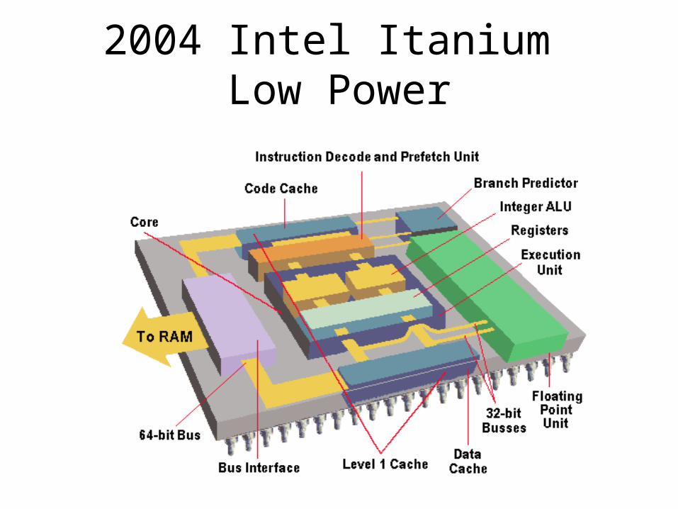
2004 Intel Itanium Low Power

Power Headaches• Problem of heat dissipation in modern semiconductors
causing manufacturers like Intel to kill faster clock speeds• Over past decades engineers have scaled microprocessor
to smaller dimensions in accordance with Moore’s Law, so that today some elements are only a few layers of atoms thick. Thinness of structures contributes to power headaches - current leakage, power consumption and high operating temperatures.
• High power consumption generates unwanted heat and decreases battery life of portable devices like notebooks and handhelds. The well-known leakage problem gets worse with successive process generations
• Big dilemma for entire semiconductor industry.• Latest Intel® Pentium® 4 processors with over 125 million
transistors built on 90nm process technology consume as much as100 watts (glowing 100W light bulb – ouch!)
• Today’s PCs - Large cooling elements, noisy fans, and massive heat sinks
• Solution??

Eureka! Enter Multicore Technology
• Dual-core and multicore chips change the game• By placing more than one computational engine or core on each die,
Intel can continue to add more and more transistors to its processors and diminish troublesome effects of processor scaling.
• Intel plans to run dual-core chips at lower frequencies than singlecore chips so they’ll require lower voltage and throw off less heat
• Two cores on a single chip will enable a processor to do more without a proportional increase in power
• Dual-core chips not the same as dual-processor systems. Many servers today have two or more processors on same motherboard These dual-processor or multi-processor systems widely used in enterprise computing environments
• By contrast, dual core components have two complete processor chips inside each package - big manufacturing change from today's single core chips
• Promises temporary relief from power and thermal challenges threatening processor performance

Era of Parallelism: 2005
• Pentium who?Pentium Extreme Edition 840 Intel dual-core chip - thoroughly Pentium 4 heritage
• Code-named "Smithfield," pair of Pentium 4 "Prescott" cores situated together on single piece of silicon. Each core has 1MB of L2 cache onboard, and two cores share an 800MHz front-side bus. Siamese twin action
• Smithfield manufactured using same basic 90nm fabrication process as current Pentium 4 chips. However, roughly twice size of Prescott core at 230 million transistors and 206 mm2 of die space
• IBM produced first multicore Power4, in 2001 (Intel aims to be first in volume production of the new chips across all market segments: server, desktop, and mobile)
Double Vision??
Smithfield

2005/06 Technology
• Parallelism revolution continues • Intel Development Forum (IDF) CA, Aug 2005• Intel CEO introduces new 65nm dual core microprocessor designed to
bring increased power per watt , production begins end 2005, in market by 2nd half 2006
• 2006 shipments (60million) based on 65nm to surpass current 90nm • Processors allow chipmakers to get more performance out of a single
piece of silicon without boosting power consumption and heat generation.
• Enables computer programs to work on more than 1 task at same time• For example, multi-core technology helps Google process data in
parallel, while controlling power and electricity costs• New processor - applied to laptops - code-named Merom• Applied to Desktop computers - code-named Conroe• Applied on Server platforms – code-named Woodcrest
Software Adjustments: Hyper-Threading• Many software vendors have already programmed their code to utilize
the multithreaded capabilities of HyperThreading technology• Hyper-Threading Technology enables software applications to execute
threads in parallel. To improve performance, threading enabled in software by splitting instructions into multiple streams so that multiple processors can act upon them.
• Delivers faster response times for multi-tasking • Multicore processors benefit from the same programming optimizations
as for HyperThreading• Dualcore will provide an immediate performance improvement to
hyperthreading applications• Operating systems such as WindowsXP and Linux have been
optimized for multicore processors and are ready to support Intel's next generation processors as soon as they are launched….
• Multicore has also raised question of software licensing and customer billing ($$). Some vendors have considered charging license fees on a per processor basis, charging more for dual or multi core systems. Microsoft has announced that its software will be licensed on a per processor package basis - only one license necessary regardless of how many cores are contained within processor.

Intel Family Overview
• >100million devices/chip (gigascale integration)• 80286 - 100,000 devices• 80386 - 275, 000 devices• 80486 - 1,000,000 devices• Pentium III – 3,000,000 devices• Pentium 4 – over 5,000,000 devices/chip (VLSI, ULSI, Gigascale)• MultiCore – Smithfield, Merom, Conroe, Woodcrest• How is a design of this complexity realized?• Must automate design, powerful CAD tools• CAD Tools research and development• Decompose design process into different levels of abstraction
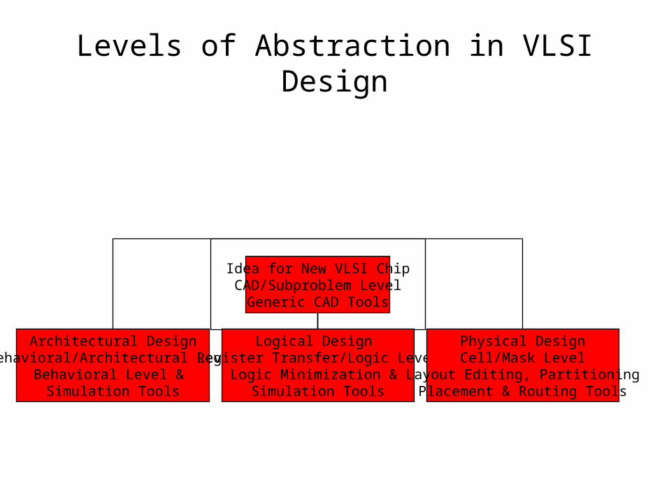
Levels of Abstraction in VLSI Design
Idea for New VLSI ChipCAD/Subproblem Level
Generic CAD Tools
Architectural DesignBehavioral/Architectural Level
Behavioral Level & Simulation Tools
Logical Design Register Transfer/Logic Level
Logic Minimization & Simulation Tools
Physical DesignCell/Mask Level
Layout Editing, PartitioningPlacement & Routing Tools

Levels of Abstraction: Architectural Design
Idea for New VLSI ChipCAD/Subproblem Level
Generic CAD Tools
Architectural DesignBehavioral/Architectural Level
Behavioral Level & Simulation Tools
Logical Design Register Transfer/Logic Level
Logic Minimization & Simulation Tools
Physical DesignCell/Mask Level
Layout Editing, PartitioningPlacement & Routing Tools

Architectural Design
• Carried out by human experts• Decisions affect Cost & performance
e.g.Architectural Design of Microprocessor
1. What should instruction set be?
2. Should instruction pipelining be employed?
3. Should processor have on-chip cache? How big?
4. Should arithmetic unit be bit-serial or parallel?• CAD Programs aid system architect• Once architecture defined, 2 tasks

Two Tasks at logic level
• Task 1• DATA PATH DESIGN• What is the datapath?• Functional Blocks, storage
elements, hardware components which allow transfer of data
• E.g. Adders, Multipliers, Shift registers, RAMs
• Data transferred using tri-state busses or mux /demux
• Task 2• CONTROL PATH DESIGN• What is the control path?• Modules which generate
control signals necessary to operate circuit
• E.g. initializing storage elements, initiate data transfer
• hardwired or micro-programmed

Design of 8-bit Adder A ← A+B
• Sum in 8bit A Reg• 8bit B Reg unchanged• Economical Design• Some Possibilities:
1. 8bit CLA Adder
2. 8bit ripple carry adder
3. Two 4bit CLA adders with ripple carry between
4. 1bit adder, perform addition serially (8 clock cycles)

Consider Option 4: Serial Adder Data & Control Paths
• Serial approach gives minimum cost, uses 2 shift registers
• Ak, Bk are kth significant bits of reg A & B• Full Adder adds Ak, Bk and Carry Ck-1 during kth
clock• Carry generated in kth cycle saved in D flip flop (init
set to 0)• Data Path: Two 8bit SR, 1FA, 1DFF, 2 Mux, 3bit
counter• Multiplexer A selects between DtaIn and Sum
output
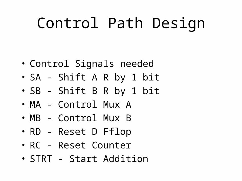
Control Path Design
• Control Signals needed• SA - Shift A R by 1 bit• SB - Shift B R by 1 bit• MA - Control Mux A• MB - Control Mux B• RD - Reset D Fflop• RC - Reset Counter• STRT - Start Addition

Control Algorithm
• forever do
while (STRT = 0) skip
Reset DFF & Counter
Set MA & MB to 0
repeat
Shift A & B Right by one
counter = counter+1
until counter = 8
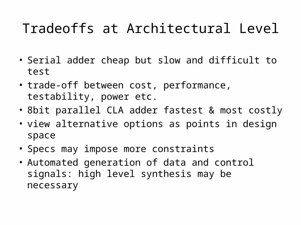
Tradeoffs at Architectural Level
• Serial adder cheap but slow and difficult to test• trade-off between cost, performance, testability,
power etc.• 8bit parallel CLA adder fastest & most costly• view alternative options as points in design
space• Specs may impose more constraints• Automated generation of data and control
signals: high level synthesis may be necessary
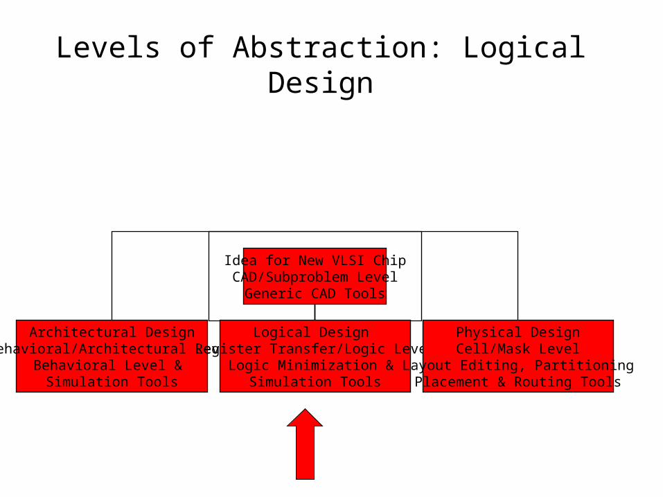
Levels of Abstraction: Logical Design
Idea for New VLSI ChipCAD/Subproblem Level
Generic CAD Tools
Architectural DesignBehavioral/Architectural Level
Behavioral Level & Simulation Tools
Logical Design Register Transfer/Logic Level
Logic Minimization & Simulation Tools
Physical DesignCell/Mask Level
Layout Editing, PartitioningPlacement & Routing Tools

Design at Logic level
• Data & Control paths contain logic blocks such as shift regs, muxs, buffers, ALU
• Q: How is cct to be implemented? As PCB, VLSI or MCM ?
• If PCB, are components available off the shelf?• If VLSI, what strategy? Full custom,standard cell
or gate array?• In either case, components placed on layout
surface and wired together
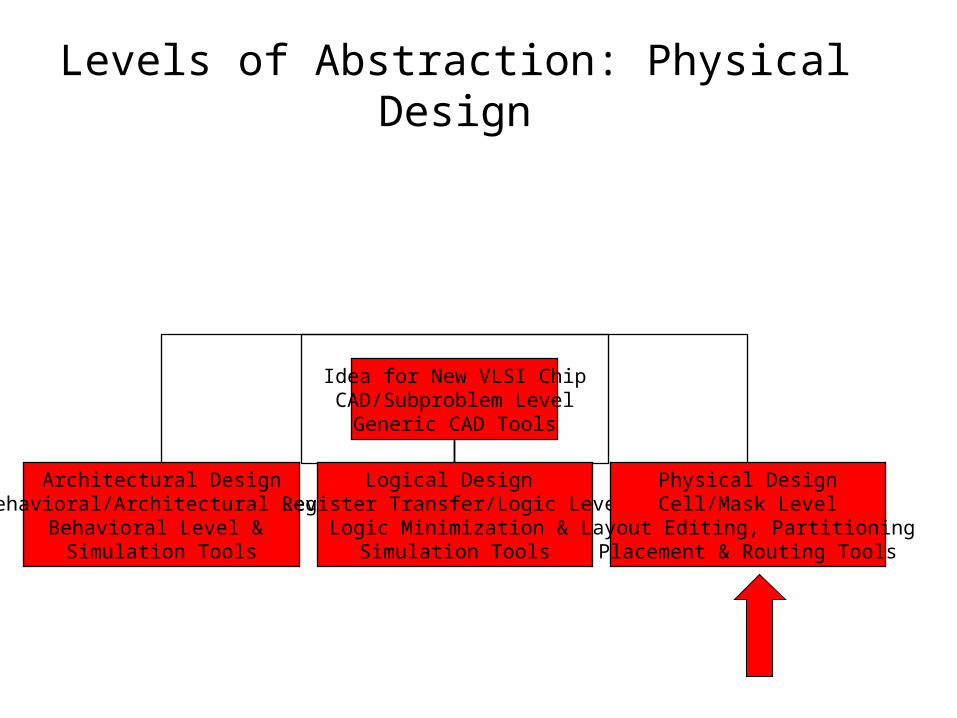
Levels of Abstraction: Physical Design
Idea for New VLSI ChipCAD/Subproblem Level
Generic CAD Tools
Architectural DesignBehavioral/Architectural Level
Behavioral Level & Simulation Tools
Logical Design Register Transfer/Logic Level
Logic Minimization & Simulation Tools
Physical DesignCell/Mask Level
Layout Editing, PartitioningPlacement & Routing Tools

Physical Design
• Refers to all synthesis steps which succeed logic design but precede fabrication e.g. partitioning, placement, routing
• Physical layout crucial in determining circuit performance, area, catastrophic yield, reliability
• 1. Circuit Performance: Timing delays, Crosstalk
metal, poly interconnect have finite impedance. Long lines have large inpedance, longer delays, crosstalk. Contacts, Vias slow signals down
• 2. Area: functional and wiring
affects yield (# of defect free chips)
large chip area = low catastrophic yield

Physical Design: Layout Effects
• low yield = high prod cost = high cct unit cost• large area = modules widely spaced = long
wires=delays and crosstalk• layout affects reliability: e.g. vias unreliable,
layout with large #’s of vias prone to defects; line widths of metal tracks must be wide enough to prevent metal migration
• course focuses on Physical, Custom Design

Physical Design Strategies
3 main approachesdiffering in 2 ways1. Layout Surface
2.structural constraints imposed on layout elements
Full CustomLayout Editing to generate physical description of Circuit
Field Prog Gate ArrayRealize cct by placing
metal connections betweentransistors prefab on wafer in 3D array
Standard cell DesignRealization using
predefined logic blocks or cells stored in library

Full Custom Layout
• Full control to the artwork designer in placing and interconnecting circuit blocks
• expert can achieve high degree of optimization in area and circuit performance
• difficult and expensive - many person months to layout ULSI chip - only used in mass prod cases
• requires powerful CAD tools - layout editor with DRC, Compaction, Extraction
• not for low prod volume ASICs• standard layout architectures to cut design time

Layout Styles: Gate array
• Mask programmable gate array or field prog• 2/3D array of unconnected transistors• Connections placed by either masking (MPGA) or applied voltage
(FPGA)• 2 types of personalization: intra-cell or inter-cell• cell library maintained, intercell wiring by layout software• after personalization, wafer diced, chips packaged• foundries stock large #’s of pre-fab wafers• quick to fabricate• few processing steps, high catastrophic yield, cheap
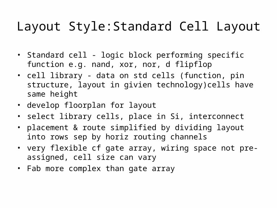
Layout Style:Standard Cell Layout
• Standard cell - logic block performing specific function e.g. nand, xor, nor, d flipflop
• cell library - data on std cells (function, pin structure, layout in givien technology)cells have same height
• develop floorplan for layout• select library cells, place in Si, interconnect• placement & route simplified by dividing layout into rows sep by
horiz routing channels• very flexible cf gate array, wiring space not pre-assigned, cell size
can vary• Fab more complex than gate array

Example of Std Cell
• Inverter function• rectangular shape• dimensions 0.6u X4.8u, CMOS
0.18u technology• lower left corner at (-1, -1)• top right corner at (0.6, 4.8)• input a available at left• output available at right• VDD & GND lines available

Macrocells, PLA & FPGA
• Macrocells - No restrictions on cell size to allow more compact layout increased cell complexity (regs, ALU’s memory) efficient layout design of complex macrocells
• PLA’s - Sum-of-Products minimal expression can be realized using 2-level logic: AND terms formed in 1st level, OR terms in 2nd level e.g. Z = A0.A1 +A0.A2 + A1.A2 easy to automate
• FPGA’s (e.g. Xilinx, Altera) 2D array of configurable logic blocks, can implement any logic fn. Channels between blocks for interconnect. I/O blocks on periphery, interconnect and logic blocks field prog by user. Cheap prototyping, re-usable,slower. 100% use of gates not possible
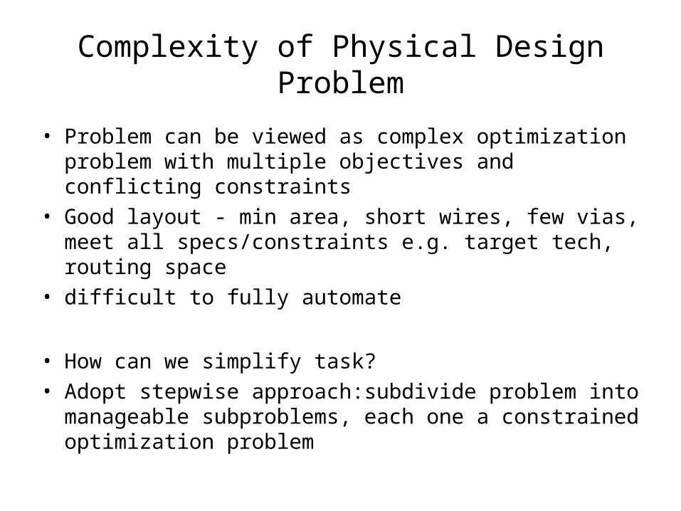
Complexity of Physical Design Problem
• Problem can be viewed as complex optimization problem with multiple objectives and conflicting constraints
• Good layout - min area, short wires, few vias, meet all specs/constraints e.g. target tech, routing space
• difficult to fully automate
• How can we simplify task?• Adopt stepwise approach:subdivide problem into
manageable subproblems, each one a constrained optimization problem
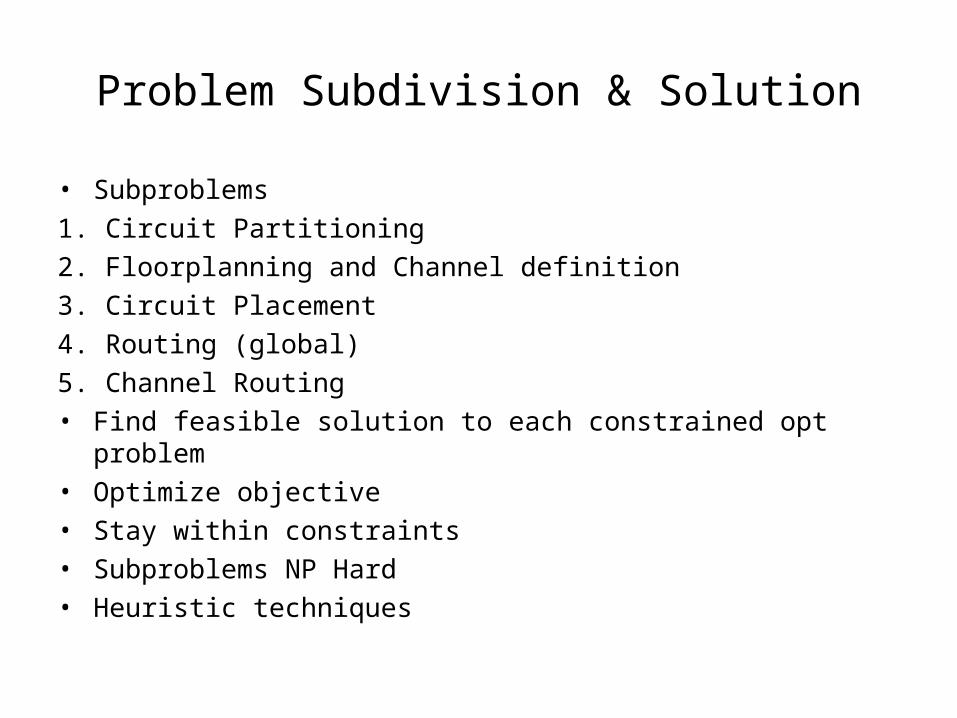
Problem Subdivision & Solution
• Subproblems
1. Circuit Partitioning
2. Floorplanning and Channel definition
3. Circuit Placement
4. Routing (global)
5. Channel Routing• Find feasible solution to each constrained opt problem• Optimize objective• Stay within constraints• Subproblems NP Hard• Heuristic techniques