Embed Size (px)
Citation preview

IAY 0600
Digitaalsüsteemide gdisain
Register TransferRegister Transfer Level Design.
FSM Synthesis.
Alexander Sudnitson
Tallinn University of Technology

Register Transfer Level
The Register Transfer Level (RTL) isThe Register Transfer Level (RTL) is characterized by
A digital system is viewed as divided into a data path (data subsystem) andinto a data path (data subsystem) and control path (controller);The state of data path consists of the contents of a set of registers;The function of the system is performed as a sequence of transition transfers (in one or more clock cycles).A i t t f i t f tiA register transfer is a transformation performed on a datum while the datum is transferred from one register to another.The sequence of register transfers is controlled by the control path (FSM).
2
A sequence of register transfers is representable by an execution graph.

Basic units of RT-level design
C t l C t lControl ControlInputs Outputs
CONTROLUNIT
Control StatusInputs Signals
Data path Data path
Inputs Outputs
DATA PATHUNIT
Inputs Outputs
3

A word description (example)
Th d i l l l fThe design ranges over several levels of representation. We begin the design process with a word description of an example device.
Digital unit performs an operation of computing the greatest common divisor(GCD) of two integers corresponding to
p
(GCD) of two integers corresponding toEuclid algorithm:The gist of this algorithm is computing the remainder from division of the greater
b ith th l d f thnumber with the less one and further exchanging the greater number with the less one and this less number with the division remainder. This converging d s o e a de s co e g gprocess is looped until the division remainder is equal to zero. That means the termination of the algorithm with the current less number as the result
4
current less number as the result.

Block diagram (example)
Start Ready
OP1 DISCRETE
OP2 ANSWSYSTEM
The interface description
entity EUCLID is
port (START: in BIT;--The first and the second operand bus
OP1, OP2: in INTEGER range 0 to 255;--Answer is ready signalAnswer is ready signal
READY: out BIT;--Answer bus
ANSW: out INTEGER range 0 to 255);
5
end EUCLID;

architecture COMMON of EUCLID is
Behavioral Description
process-- Temporary variables:variable RG1, RG2, temp: INTEGER range 0 to 255;begin
W i i f h-- Waiting for the start:wait on START until START’event and START = ‘1’;RG1 := OP1; RG2 := OP2; if RG1 /= RG2 thenif RG1 < RG2 thenif RG1 < RG2 then
-- Exchange operands:temp:=RG1; RG1 := RG2; RG2:=temp;
end if;while RG1 /= 0 loopp-- Calculation of the reminder:
RG1 := RG1 rem RG2;if RG1 /= 0 then
temp:=RG1; RG1 := RG2; RG2:=temp;end if;
end loop;end if;--Answer output:ANSW < RG2; READY < ‘1’;
6
ANSW <= RG2; READY <= ‘1’;end process;
end COMMON;

The flowchart (example) BEGIN
Yes
BEGIN
START No
RG1 := OP1;RG2 := OP2;
RG1 RG2Yes NoRG1 = RG2Yes
RG1 < RG2 RG1 := RG2;RG2 := RG1;
Yes
No
Remainder Computation
Remainder = 0 NoYes
READY := 1;ANSW := RG2;
7
END

GCD computation of 15 and 24
OP1 OP2RG1 RG2
15 24RG1 < RG2
RG1 := RG2; RG2 := RG1;1524
Remainder = 99 15
RG1 /= 0RG1 := RG2; RG2 := RG1;15 9
Remainder = 66 9
RG1 /= 0RG1 := RG2; RG2 := RG1;
9 6Remainder = 3
3 6RG1 /= 0
RG1 := RG2; RG2 := RG1;6 36 3
Remainder = 00 3
RG1 = 0READY := 1; ANSW := 3;
8

Data path -1-
The data path is specified by the set of operations presented in the behavioral descriptions and by the set of basic elements which it will be implemented by.elements which it will be implemented by.
Notice that remainder computation chip (or macro) doesn’t exist. We need to synthesize it on the next design step basing upon its behavioural description and existing (or virtual) elements of the lower level - e g adders shift registers counterslevel e.g. adders, shift registers, counters. It would in its turn lead to appearing the control part of the lower level and so on (top-down design methodology).
9
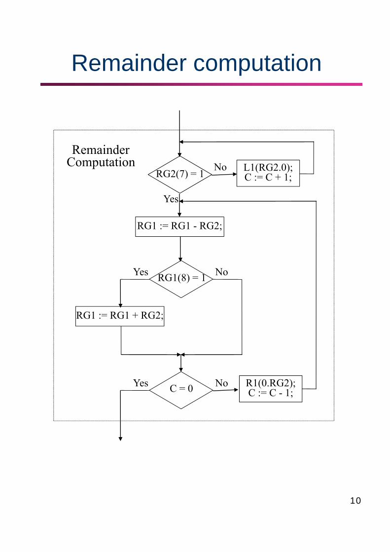
Remainder computation
NoRG2(7) = 1 L1(RG2.0);C C + 1
RemainderComputation
RG1 := RG1 - RG2;
RG2(7) = 1
Yes
C := C + 1;
RG1(8) = 1Yes No
RG1 := RG1 + RG2;
C = 0 No R1(0.RG2);C := C - 1;
Yes
10

The flowchart BEGIN
Yes
RG1 := OP1;RG2 := OP2;
Yes No
START No
RG1 = RG2Yes No
RG1 < RG2RG1 := RG2;RG2 := RG1;Yes
No
RemainderComputation No
RG1 := RG1 - RG2;
RG2(7) = 1
Yes
L1(RG2.0);C := C + 1;
RG1(8) = 1Yes No
RG1 := RG1 + RG2;
C = 0 No R1(0.RG2);C := C - 1;
Yes
11
Remainder = 0 NoYes
READY := 1;ANSW := RG2;
END

Data path -2-
Consider in our example the data path that is based upon some ALU which completes four arithmetic operations (addition, subtraction, left shift and right shift) with registers RG1 and RG2 for storing the intermediate results, with up/down counter and with control buses for data transfer It isand with control buses for data transfer. It is considered that RG1 and RG2 are Master-Slave registers that allows to exchange their contents during one clock cycle.
Input operands are 8-bit wide. For this example it is assumed that input operands are positive and none of them is 0 Noteare positive and none of them is 0. Note, that RG1 and RG2 have a sign bit, as remainder computation algorithm deals with negative values as well.
12

The structure of GCD device CONTROL
FSM ●
y0y1x1
x0
●
START
CONTROL UNIT
FSM ●●
y10X5
●●
READY
x1RG1
y9 y8y5 y4
y0 x4 x6OP1
ALU x2
RG2
7 6y1 x3
OP2
Counter
y7 y6y
y10DATA PATH UNIT
ANSW
y3 y2
x5
13
y y

ALU
x2 x1
OP1 >= OP2 0
OP1 < OP2 1
0 OP1 /= OP2
1 OP1 = OP2
ALU
Result
9
y8ALUy9
OP1 OP2
R1L1+
0
1
1
0
0
0
1
1
R1L1–+
y8
y9
14

Registers and Counter
x4NOR
x6
x3
RG1
enable
Sign
RG1
enable
Sign
y0enable
y1enable
0 C + 1
y3
Counter NOR x5
1 C – 1
y2enable
15

Multiplexers
y5 y4
OP1 RG2
ALU
RG2
RG1 Input
OP1 RG2 Input
OP2
y6y7
01
1–
0 0 ALURG1
RG1
RG2
OP2 RG1 Input
OP1
y4y5
01
1–
0 0 ALURG2ALU
RG1
RG2 Input
OP2
G
y7 y6
16
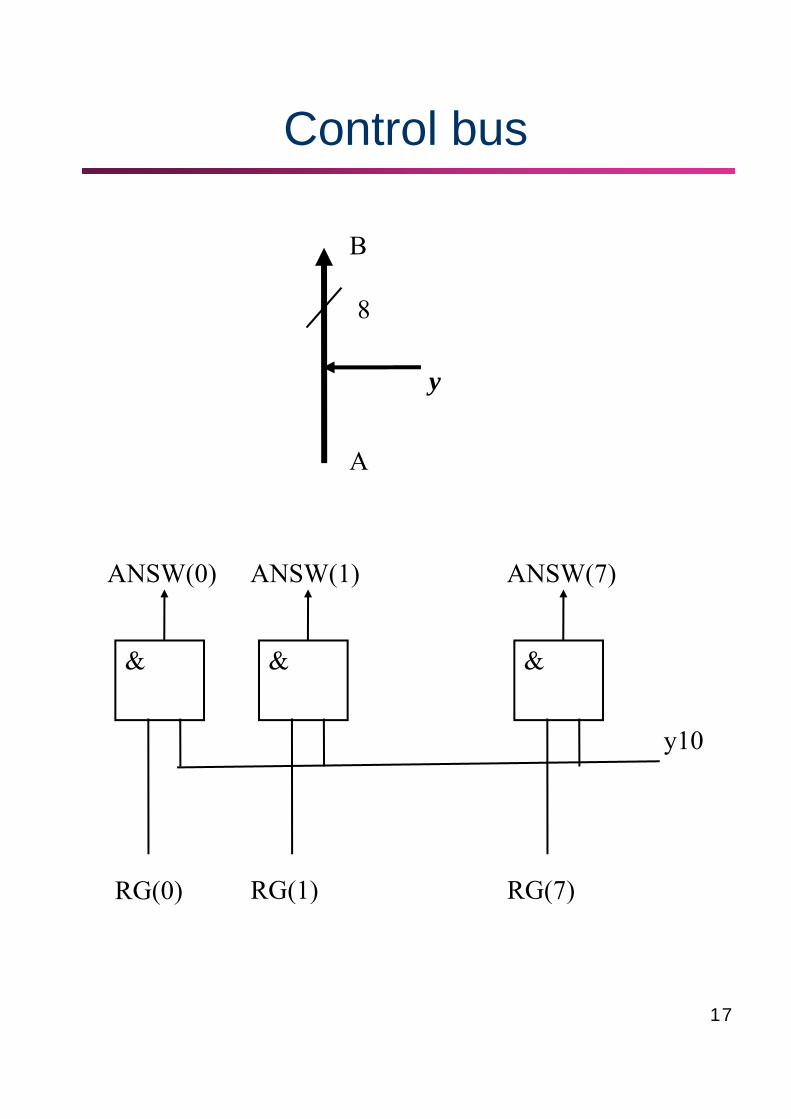
Control bus
8
B
A
y
ANSW(0) ANSW(1) ANSW(7)
y10
& & &
RG(0) RG(1) RG(7)
17
( ) ( ) ( )

Control part
At every description level after the (regular)At every description level after the (regular) structure of data path is defined it is possible to extract the remaining control part from the current level of behavioral description. Naturally this extracted control part description may be at firstextracted control part description may be at first only behavioral one and the methods of finite automata synthesis are required for control part (controller) implementation.
In this stage it is convenient to represent theIn this stage it is convenient to represent the extracted control behavior by means of graph-scheme of algorithm (GSA).
The flowchart corresponding to our algorithm was bt i d th fi t t f GSA th iobtained as the first step of GSA synthesis.
In this flowchart simultaneously executed statements are grouped into common blocks.
The GSA we got from the flowchart by replacing the computational statements (actions of ALU and counter) with the corresponding control signals (y-s) and the conditions - with binary
18
conditions signals (x-s).
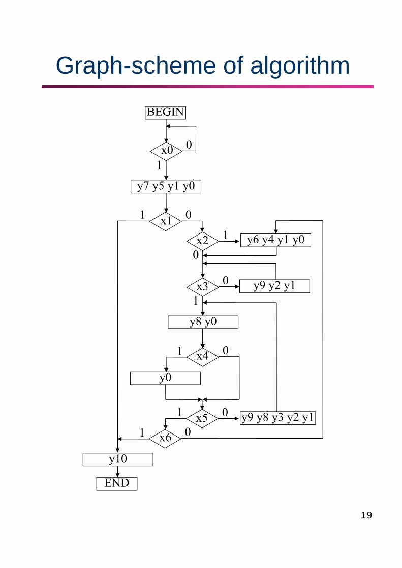
Graph-scheme of algorithm
BEGINBEGIN
x0 0
1
y7 y5 y1 y0
x1x2
01
1 y6 y4 y1 y0
x3
0
y9 y2 y10
1
8 0
x4
y8 y0
01
y0
y9 y8 y3 y2 y1x5 0
x6
101
y10
19
y10
END

Moore type FSM synthesis
Step 1. The construction of marked GSA.
At this step, the vertices “Begin”, “End” and oerator vertices are marked by the symbols s1, s2, … as follows:,
vertices “Begin”, “End” are marked by the same symbol s1;
the symbols s2, s3, … mark all operator vertices;
all operator verteces should be marked;
Note that while synthesizing a Moore FSM b l f t t k t i t f tisymbols of states mark not inputs of vertices
following the operator ones but operator vertices.
Step2. The construction of transition list (state diagram) of a controller.
Spres SnextX(Spres, Snext)
Y(Spres) Y(Snext)
20
p

Moore type FSM GSABEGIN S1BEGIN
x0 0
1
7 5 1 0
S1
S2y7 y5 y1 y0
x1
x2
01
1 y6 y4 y1 y0
S2
S3
x3
0
y9 y2 y10
1S4
x4
y8 y0
01
y0
S5
S6
y9 y8 y3 y2 y1x5
y
0
x6
1
01S7
21
y10
END
S8
S1

The transition list (Moore FSM)
PresentState
Next State
Input Conditions
OutputValue
S1 S2S1
x0¬ x0 —
S2 S8S3S5S4
x1¬ x1 & x2¬ x1 & ¬ x2 & x3¬ x1 & ¬ x2 & ¬ x3
y7 y5 y1 y0
S3 S5S4
x3¬ x3 y6 y4 y1 y0
S4 S5S4
x3¬ x3 y9 y2 y1
S5 S6S7S8S3
x4¬ x4 & ¬ x5¬ x4 & x5 & x6¬ x4 & x5 & ¬ x6
y8 y0
S6 S7 5S6 S7S8S3
¬ x5 x5 & x6 x5 & ¬ x6
y0
S7 S5 1 y9 y8 y3 y2 y1
22
S8 S1 1 y10
Microoperation and microinstruction
Let a microoperation be an elementaryLet a microoperation be an elementary indivisible step of data processing in the datapath and let Y be a set of microoperations.
Microoperations are induced by the binary signals y1, … ,yT from a controller.
To perform the microoperation yi (i = 1, …, T) the signal yi = 1 has to appear at the output yi . g yi pp p yi
A set of microoperations executed concurrently in the datapath is called a microinstruction.p
Thus if βh = {yh1, … , yh
t} is microinstruction, then βh is represented as subset of Y and the microoperations yh
1, … , yht are executed at the
same clock period. The Yt could be empty and we denote such an empty microinstruction Y0 (“-“).
23