Embed Size (px)
Citation preview

TA/SEK.TUR/TE/2009/010
PENGENDALIAN LEVEL KETINGGIAN AIR MENGGUNAKAN
KONTROL PID
TUGAS AKHIR
Diajukan Sebagai Salah Satu Syarat Untuk Mempcroleh Gelar Sarjana
Pada Jurusan Teknik Elektro Fakultas Teknologi Industri
Universitas Islam Indonesia
Disusun Oleh :
Nama : Syaiful Mansyur
No Mahasiswa : 04524067
JURUSAN TEKNIK ELEKTRO
FAKULTAS TEKNOLOGI INDUSTRI
UNIVERSITAS ISLAM INDONESIA
YOGYAKARTA
2009

LEMBAR PENGESAHAN PEMBIMBING
PENGENDALIAN LEVEL KETINGGIAN AIR MENGGUNKAN
KONTROL PID
TUGAS AKHIR
Disusun oleh :
Nama : Syaiful Mansyur
No. Mahasiswa : 04524067
Yogyakarta, April 2009
Pembimbing I PembimbinaJl
Dr. Agung Alfiansyah. PEA

LEMBAR PENGESAHAN PENGUJI
PENGENDALIAN LEVEL KETINGGIAN AIR MUNGGUNAKAN
KONTROL PID
TUGAS AKHIR
Oleh:
Nama : Syaiful Mansyur
No. Mahasiswa : 04524067
Telah Dipertahankan di Depan Sidang Penguji Sebagai Salah Satu Syarat
Untuk Memperoleh Gelar Sarjana Teknik Elektro
Fakultas Teknologi Industri Universitas Islam Indonesia
Yogyakarta, April 2009
Tim Penguji,
Ir. Budi Astuti. MT
Ketua
Dr. Agung Alfiansyah, PEA
Anggota I
Tito Yuwono, ST.. MSc
Anggota II
Mengetahui,
Jurusan Teknik Elektro
Islam Indonesia
Ml
/

HALAMAN PERSEMBAHAN
Tiigas a£/iir iniJ%.nandaj?ersemfiafi&an 3Cepada
^ya^anda dan Ifunda tercinta
]/ang setafii men/adi inspirasidatam /itdupku
JCa£a££u ,adi&£u, fieserta Mefaarga SesarMu yang
se/afa memfieri&anjterfiatiarL, semangat, motivasidan
do a untu&Mu
Tim 2to0ot V/Iatas seman^at dan I(muyang tag
terfiin^ga

Motto
"Sesungguhnya orang yang dirongganya tidak terdapat Al-
Qur' an
adalah seperti rumah yang rusak"
iHR. Ahmad, Tarmidzi dan Ad-Darmini)
"Dan jadikaniah sabar dan shalat sebagai penolongmu, dan
sesungguhnya yang demikian itu sungguh berat, kecuali
bagi orang-orang yang khusyu"
{Q.S. Al-Baqarah: 45)
"Saya hanya tahu satu hal, yaitu saya tidak tahu apapun"
(Socrates.)
"Sebaik-baiknya manusia adalah orang yang banyak
manfaatnya (kebaikannya kepada orang lain)"
(H.R. Qodla'ie dari Jabir)
"Sesungguhnya susudah kesusahan itu ada kemudahan"
{Q.S Asy Syarh; 5)

kai \pi;n<;am\\r
Ml jfcfyk
assalamu'alaikum warahmatullahi wabarakaluh
Puji syukur penulis panjatkan kehadirat Allah SWT yang telah memberikan
Rahmat dan Hidayah-Nya sehingga penulis dapat menyelesaikan Tugas akhir yang
berjudul "Pengendalian Level Ketinggian Air Menggunakan Kontrol PID ".
Shalawat dan salam selalu terhaturkan kepadajunjungan kita Nabi Muhammad SAW
yang menjadi uswatun hasanah bag! kita semua hingga akhir zaman.
Penyelesaian Tugas akhir ini merupakan salah satu syarat untuk memperoleh
gelar sarjana Teknik Elektro pada Fakultas Teknologi Industri Universitas Islam
Indonesia. Dengan selesainya Tugas akhir ini, maka seluruh aktivitas studi pada
institusi tercinta ini berakhir dan membuka pintu untuk masuk ke tantangan
berikutnya. Proses penyelesaian tugas akhir ini merupakan serangkaian integrasi
antara teori serta praktek yang telah didapatkan semasa duduk dibangku kuliah. Ilmu
dan amal menjadi poin penting akhir dari penyelesaian tugas akhir ini.
Tugas akhir ini merupakan implementasi dari proses perancangan serta
pengujian sistem. Aplikasi utama dari sistem ini banyak dimanfaatkan dalam dunia
industri, meskipun skala pengerjaan tugas akhir ini hanya sebatas simulasi. Namun,
VI

begitu pentingnya fungsi dari perangkat ini, menjadikan penulis mencoba
menganalisis sekaligus memodelkan sebuah perangkat yang dapat dimanfaatkan
sebagai referensi dalam ilmu pengetahuan dan teknologi.
Penulis menyadari sepenuhnya bahwa isi dari tugas akhir ini masih jauh dari
sempurna, namun dengan niat yang tulus dan ikhlas, penulis menerima segala macam
kritik dan saran yang membangun demi kelangsungan dan kemajuan ilmu
pengetahuan dan teknologi.
Pada kesempatan ini penulis ingin menyampaikan rasa terima kasih yang tak
terhingga kepada:
1. Allah SWT, yang dengan izin dan kuasa-Nya masih memberi kesempatan
untuk menyelesaikan tugas akhir ini.
2. Baginda Nabi besar Muhammad SAW, atas cahaya Islam.
3. Kedua orangtua ku, papa Mansyur dan mama Nursiah tercinta yang senantiasa
memberikan dukungan, semangat, moril, materil dan do'a setiap saat.
Terimakasih atas kesabaran kalian.
4. Bapak Tito Yuwono,.S,T,.M.Sc selaku Ketua Jurusan Teknik Elektro.
Fakultas Teknologi Industri
5. Ibu Ir. Budi Astuti, MT. dan bapak DR. Agung Alfiansyah, DEA. selaku
dosen pembimbing yang sangat memberikan banyak inspirasi serta motivasi
dan ilmu.
VII

6. Kedua kakakku mbak Meny dan mbak Pety dan adikku Kiki, serta seluruh
keluarga besarku yang selalu mendoakan dan memberikan dukungan dalam
penyusunan tugas akhir ini.
7. The special one Erma Oktariani yang telah memberikan perhatian selama ini.
Semangat yah kerjain skripsinya
8. Seluruh Dosen dan karyawan FTI-UII yang bersedia dengan sabar membantu
dan membagi ilmunya.
9. Mas Agung yang sering membantu dan menemani di Lab. IMEL hingga
malam, terimakasih atas komponen elektronikanya.
10. Alvin Sahroni,ST , seorang sahabat yang telah banyak membantu. Selamat
menempuh hidup baru kawan. Semoga menjadi keluarga yang sakinah,
mawaddah, warohmah dan dianugerahi keturunan yang sholeh dan sholehah.
Amin.
11. Teman-teman gen' kapak, Hendra, Tino, Danis, Seto, Pati, Dhani, Sinjo,
Dody, semoga kita bias sukses bersama suatu saat.
12. Seluruh teman-teman elektro 04 yang menjadikanku seorang yang bermanfaat
buat kalian semua.Terima kasih atas dukungan serta apa yang telah kita
ciptakan bersama.
13. Zakki sang programmer handal,
14. Kru Laboratorium Instalasi dan Mesin Listrik, Mas Agung dan asisten A'i,
Roby, Riski, Mawan.
VIII

DAFTAR ISI
HALAMANJUDUL
LEMBAR PENGESAHAN DOSEN PEMBIMBING
LEMBAR DOSEN PENGUJI 111
HALAMAN PERSEMBAIIAN
HALAMAN MOTO v
KATA PENGANTAR vi
ABSTRAK x
DAFTAR ISI xi
DAFTAR GAMBAR xiii
DAFTAR TABEL xvi
BAB IPENDAHULUAN
1.1 Latar Belakang Masalah U{
1.2 Maksud dan Tujuan (2
1.3 Perumusan Masalah 2
1.4 Batasan Masalah 2
1.5 Langkah Penelitian 3
1.6 Sistematika Penulisan Laporan 3
BAB II STUDI PUSTAKA
2.1 Pengendali Ketinggian Air menggunakan Kontrol PID 5
2.1.1 Sistem Pengendali 7
2.1.2 Kontrol PID ( Proporsional Intergal Derivative ) 10

2.1.3 Kontrol P (Kontrol Proporsional) 11
2.1.4 Kontrol I (Kontrol Integral) 13
2.1.5 Kontrol D (Kontrol Derivative) 14
2.1.6 Kombinasi Kontrol P, I, dan D 15
2.2 Potensiometer 16
2.3 ADC (Analog to Digital Converter) 17
2.3.1 ADC 0804 17
2.4 DAC (Digital to Analog Converter) 20
2.4.1 DAC 0808 20
2.5 PPI8255 22
2.6 PortParalel 24
2.7 Rencana Penelitian 27
BAB III METODOLOGI
3.1 Perancangan Alat 29
3.2 Perancangan Sensor *"29
3.3 Perancangan Rangkaian ADC ^30
3.4 Perancangan Rangkaian Driver Pompa Air s31
3.5 Perancangan Rangkaian Solenoid Valve 131
3.6 Perancangan Rangkaian DAC 32
3.7 Perancangan Perangkat Lunak 33

BAB IV ANALISA DAN PEMBAHASAN
4.1 Analisis Pada Sisi Perangkat Keras 38
4.1.1 Setting Potensiometer 38
4.1.2 Akuisisi Data Rangkaian ADC 38
4.1.3 Solenoid valve sebagai output 42
4.2 Analisis Perangkat Lunak 43
4.3 Analisis Parameter PID untuk Optimasi Sistem 42
4.3.1 Pengujian Sistem Kontrol PID 43
4.3.1.1 Pengujian Sistem dengan perubahan settingpoint 46
4.3.1.2 Pengujian Sistem dengan Perubahan Parameter 49
4.3.1.2.1 Perubahan Parameter Kp 49
4.3.1.2.2 Perubahan Parameter Ki 52
4.3.1.2.3 Perubahan Parameter Kd 53
4.3.2 Pengujian Sistem Kontrol PI 54
BAB V PENUTUP
5.1 Kesimpulan *^57
5.2 Saran 58
DAFTAR PUSTAKA
LAMPIRAN

DAFTAR GAMBAR
Gambar 2.1 Blog Diagram Utama 5
Gambar 2,2 Kurva karakteristik respon 9
Gambar 2.3 Kontrol Proporsional, P 10
Gambar 2.4 Kontrol Integral, I 12
Gambar 2.5 Kontrol Derivative, D 13
Gambar 2.6 Kontrol PID 14
Gambar 2.7 Bentuk Fisik Potensiometer 15
Gambar 2.8 Konfigurasi pin ADC 0804 16
Gambar 2.9 Konfersi Rangkaian R-2R Ladder 19
Gambar 2.10 DAC 0808 19
Gambar 2.11 Rangkaian Penguat Inverting 21
Gambar 2.12 Nomor Pin Port Paralel 22
Gambar 3.1 Sistem Pengatur 27
Gambar 3.2 Rangkaian Sensor Potensiometer 28
Gambar 3.3 Rangkaian ADC 0804 29
Gambar 3.4 Rangkaian Driver Pompa Air 30
Gambar 3.5 Rangkaian Driver Solenoid valve 31
Gambar 3.6 Rangkaian DAC 0808 31
Gambar 3.7 Perancangan GUI 32

Gambar 3.8 Diagram Alir program kontrol 33
Gambar 3.9 Diagram Alir Program ADC 34
Gambar 4.1 Pengujian potensiometer dengan DAQ NI 6009 39
Gambar 4.2 Tampilan GUI Kontrol PID 40
Gambar 4.4 Respon output sistem dengan Kp=85, Ki=10, Kd=3 46
Gambar 4.5 Grafik ADC setelah di Run 48
Gambar 4.6 Tampilan GUI Kontrol PID dengan Kp-60,Ki=6,Kd=40 50
Gambar 4.7 Respon Output PID dengan Kp=60,Ki=6,Kd=10 51
Gambar 4.8 Respon Output PID dengan Kp=60,Ki=20,Kd=10 52
Gambar 4.8 Respon Output PI dengan Kp=70,Ki=8 53
DAFTAR TABEL
Tabel 2.1 Tanggapansistemkontrol PID terhadap perubahan parameter 10
Tabel 2.2 Fungsi Pin Pada Port paralel 22
Tabel 2.3 Alamat Pada Port Paralel 24
Tabel 2,4 Register Port Printer 24
Tabel 4.1 Hasil Pengujian Sensor 37
Tabel 4.2 Hasil Pengujian Pada Rangkaian ADC 0804 38
Tabel 4.3 Hasil Pengujian terhadap settingpoint PID 44
Tabel 4.4 Hasil Pengujian terhadap parameter Kp 47

ABSTRAK
Tugas akhir ini menjelaskan tentang aplikasi sistem kontrol pada pengaturan levelketinggian air. Metode kontrol yang digunakan dalam sistem ini adalah kontrolproporsional integral derivatif (PID). Penggunaan kontrol PID dapat membuat sistemmenjadi dinamik atau stabil dengan memasukkan parameter kontrol yang tepat.Pengujian sistem telah dilakukan untuk mengontrol level airdengan ketinggian antara0 - 30 cm atau dengan memasukkan setting point 0-50 %, pengujian inimenggunakan dua tangki air dimana tangki bawah sebagai penampung dan tangkiyang bagian atas adalah tangki untuk ketinggian air yang telah diukur. Semua proseskontrol dan akuisisi data dilakukan dengan menggunakan komputer (PC) danDELPHI7 sebagai tampilan visualnya. Dari hasil pengujian didapatkan bahwaparameter kontrol PID yang tepat untuk pengontrolan sistem ini adalah, Kp - 80, Ki= 10, Kd = 3 dan pada tangki air terbaca 14cm. Pada pengontrolan kontrol PI makaparameter yang tepat di sistem ini adalah, Kp = 70, Ki -8 dan padatangki air terbaca15cm.
Kata kunci: sistem kontrol, kontrol proporsional integral derivatif (PID), kontrollevel air.

BAB I
PENDAHULUAN
1.1 Latar Belakang
Dalam eraglobalisasi, sektor industri memegang peranan yang sangat penting
khususnya di Indonesia. Didalam industri, sangat dibutuhkan sistem kontrol yang
baik untuk dapat menunjang proses berjalannya industri tersebut dan untuk
meningkatkan efisiensi dalam proses produksi. Karena itu dalam hal ini akan dibuat
suatu sistem kontrol yang diharapkan dapat memberikan kontribusi dalam dunia
industri.
Perkembangan teknik kontrol sudah merambah dari peralatan industri yang
kompleks, perlengkapan militer sampai ke peralatan rumah tangga. Beberapa sistem
kontrol yang mudah di jumpai diantaranya adalah pengatur suhu, pengatur
kelembaban ruangan, pengendalian level air, pengatur gerakan robot, dan lain
sebagainya. Sistem kontrol dibutuhkan untuk memperbaiki tanggapan sistem dinamik
agar didapat sinyal keluaran seperti yang diinginkan. Sistem kontrol yang baik adalah
yang mempunyai tanggapan yang baik terhadap sinyal masukan yang beragam.
Dalam perancangan sistem kontrol ini diperlukan gambaran tanggapan sistem dengan
sinyal masukan dan aksipengontrolan yang meliputi:
1) Kestabilan sistem yang dirancang.
2) Tanggapan sistem terhadap berbagai jenis aksi pengontrolan.

1.2 Perumusan Masalah
Dari uraian singkat diatas, maka permasalahan yang akan dibahas dalam
penulisan ini dapat di jelaskan sebagai berikut :
1) Bagaimana mendapatkan sebuah pengendalian yang sempurna dalam
sebuah kontrol pengendalian level air.
2) Bagaimana mencari fungsi alih dari sistem tersebut.
3) Bagaimana merancang sebuah tangki air yang sebenamya agar dapat
menjadi simulasi untuk sistem pengontrolan ini.
1.3 Tujuan dan Manfaat
Adapun tujuan dan manfaat dari penelitiandan perancangan sistemini adalah:
a. Dapat membangun suatu sistem pengendalian berbasis kontrol PID
yang dapat mengendalikan tinggi rendah air.
b. Mampu menerapkan sistem pengendalian ini kedalam dunia industri
saat ini.
c. Mendapatkan sistem pengontrolan yang baik untuk sebuah sistem
yang belum dinamik.
1.4 Batasan Masalah
Pembahasan dalam penelitian dan perancangan ini dibatasi oleh :
a. Sensor yang digunakan untuk mengukur ketinggian air adalah
potensiometer.

b. Pengujian sistem ini dilakukan untuk mengontrol level air dengan
ketinggian 0 - 50% pada tampilan tangki visual.
c. Metode pengaturan yang digunakan adalah PID (Proporsional
Integral Derivative) yang diimplementasikan secara digital.
d. Metode tunning atau penyetelan kontrol PID yang digunakan adalah
metode manual (trial & error).
e. Instrumen pengatur untuk semua proses kontrol dan akuisisi data
dilakukan dengan menggunakankomputer (PC).
f. Pengujian instrumen hanya dilakukan pada plant air dan pipa masukan
serta keluaran yang memiliki ukuran tertentu.
g. Pengamatan hanya dilakukan pada gelombang keluaran pada valve
yang diatur.
h. Settingpoint terbatas pada pembacaan ADC antara 0-255 bit.
1.5 Sistematika Penulisan
Sistematika penulisan tugas akhir dengan judul "pengendalian level
ketinggian air menggunakan kontrol PID" ini adalah sebagai berikut:
BAB I PENDAHULUAN
Bab ini membahas tentang latar belakang masalah yang akan diteliti,
rumusan masalah, batasan masalah, tujuan dan manfaat penelitian, dan sistematika
penelitian.

BAB II STUDI PUSTAKA
Bab ini memuat sistem kerja dan analisis dari penelitian dan tugas akhir
yang sejenis yang sudahdibuat. Dari analisis ini akanditentukan padatugas akhir ini.
BAB III METODOLOGI
Bab ini menjelaskan perancangan hardware dan software yang digunakan,
bagian-bagian yang terlibat dalam sistem beserta cara mengimplementasikan dari
setiap bagian tersebut.
BAB IV PENGUJIAN, ANALISIS DAN PEMBAHASAN
Bab ini membahas mengenai hasil-hasil pengujian yang diperoleh dari uji
coba perakitan dibandingkan dengan dasar teori sistem.
BABV PENUTUP
Bab ini memuat kesimpulan dan saran-saran dari proses perancangan yang
telah dilakukan.

BAB II
STUDI PUSTAKA
2.1 Pengendali Level Ketinggian Air dengan Menggunakan Kontrol PID
Perancangan pengendalian level air telah banyak dilakukan salah satunyapada
penelitian yang telah ada yaitu "Pengendali Level Ketinggian Air dengan
Menggunakan Kontrol PID",( Thiang, Yohanes TDS, Andre Mulya, 2004). Makalah
ini menjelaskan tentang aplikasi sistem kontrol pada pengaturan level ketinggian air.
Metode kontrol yang digunakan dalam sistem ini adalah kontrol proporsional -
integral - derivatif (PID). Semua proses kontrol dan akuisisi data dilakukan dengan
menggunakan komputer (PC). Pengujian sistem telah dilakukan untuk mengontrol
level air dengan ketinggian antara 0-30 cm. Pengujian dilakukan dengan beberapa
variasi parameter kontrol PID dengan input berupa fungsi step. Dari hasil pengujian
didapatkan bahwa parameter sistem kontrol level ketinggian air yang paling tepat
adalah Kp = 10, Ki = 0,1 dan Kd - 5.
Sistem kerja dari perancangan alat tersebutadalah sebagai berikut:
Gambar 2.1 Btok diagram Utama

Gambar 2.1 menunjukkan blok diagram sistem yang telah dibuat. Plant terdiri
dari dua buah bejana atau tangki yang terbuat dari kaca. Tangki yang bawah
merupakan tempat penampungan air berukuran 39 x 34 x 35 cm. Tangki yang di atas
berfungsi sebagai plant yang diatus level ketinggian airnya. Tangki ini berukuran 19
x 14 x 40,5 cm. Sebuah pompa digunakan untuk menaikkan air dari tangki
penampungan ke dalam tangki plant. Spesifikasi pompa yang digunakan adalah 12
VDC, 3,5 A. Untuk mengatur pembuangan air digunakan sebuah stop kran dan
sebuah solenoidvalve. Stopkran digunakan untuk pembuangan air secara manualdan
solenoid valve untuk pembuangan air yang dikontrol melalui personal computer
(PC). Sensor yang digunakan untuk mengukur ketinggian air adalah potensiometer.
Untuk mengkonversi gerakan naik-turun ketinggian air menjadi gerakan rotasi yang
akan memutar potensiometer, digunakan sebuah pelampung dan pemberat yang
dirangkai dalam sebuah sistem katrol. Besar potensiometer yang digunakan adalah 5
kQ. Rangkaian potensiometer yang mengubah ketinggian air menjadi tegangan.
Rangkaian ini mengeluarkan tegangan output sebesar 0 - 1,194 volt untuk range
pengukuran ketinggian air dari 0-30 cm.
Dalam perancangan alat sebelumnya ada sebuah kran air manual untuk
pembuangan air yang nanti akan digunakan untuk pengujian sistem dengan
gangguan, pompa air yang digunakan adalah pompa air DC 12Volt, serta solenoid
valve nya mempunyai spesifikasi sistem tegangan AC 220 Volt.

Sedangkan pada tugas akhir yang dibuat sekarang tidak digunakan kran air
manual sehingga tidak memperhitungkan pengujian sistem dengan gangguan,
spesifikasi pompa air yang digunakan yaitu AC 220 Volt, serta solenoid valve DC 12
Volt. Hal ini dilakukan karena pada tugas akhir ini pengujian dilakukan dengan
mengatur ouput keluaran yang dilakukan oleh solenoid valve, sedangkan input
masukannya konstan dari pompa air. Perbedaan lain lagi dari sistem sebelumnya
yaitu pada tampilan visual. Pada alat sebelumnya tidak memiliki tampilan visual pada
PC atau hanya menampilkan grafik PID. Sedangkan pada alat ini terdapat visual
tangki yang real time yakni kita dapat memonitor langsung ketinggian air yang
ditampilkan di PC secara real time. Serta terdapat pula tampilan grafik dari keluaran
ADC serta grafik kontrol PID.
Untuk tampilan visualisasi dan simulasi kontrol PID pada tangki air, penulis
mengadopsi simulasi pengendali PID yang dikembangkan oleh Andrew R Clayton
(http://\vww.torr\\ne//authorsmore.php?id 691 i)
2.1.1 Sistem Pengendali
Pengendali merupakan komponen sistem yang berfungsi mengolah informasi
yang berasal dari sinyal state (state sistem, state input, state output), menjadi sinyal
kontrol sedemikian rupa sehingga karekteristik dinamik sistem hasil desain
memenuhi spesifikasi performansi tertentu. Dalam perencanaan sebuah sistem
kendali, hal pertama yang hams dilakukan adalah mendefinisikan struktur sistem
tersebut secara tepat. Perencanaan ini biasanya dilakukan agar memenuhi terhadap
spesifikasi berikut:

• Ketelitian
• Kecepatan member! jawaban
• Settling time paling lama
• Stabilitas
Dalam setiap perancangan pegendali atau spesifikasi kontroler, diperlukan
suatu spesifikasi kontrol yang digunakan sebagai acuan perancangan. Pada
perancangan kontroller untuk mengetahui level ketinggian air dengan mengatur valve
keluaran tank, digunakan spesifikasi performance untuk respon transient sebagai
acuan untuk mendapatkan suatu kontroller yang baik. Respons transient suatu sistem
kontrol secara praktek selalu menunjukkan osilasi teredam sebelum mencapai
keadaan mantap (steady state).
Menurut Ogata, parameter-parameter yang diperlukan untuk menganalisa
karakteristik performansi sistem kontrol sebagai berikut:
1) Waktu tunda (delay time), td : adalah waktu yang diperlukan oleh
respons untuk mencapai setengah nilai akhir untuk waktu yang
pertama.
2) Waktu naik (rise time), tr : adalah waktu yang diperlukan oleh respon
untuk naik dari 10% menjadi 90%, 5% menjadi 95%, atau 0% menjadi
100% dari nilai akhir yang biasa digunakan. Untuk sistem atas
redamanwaktu naik yangbiasadigunakan 10% menjadi 90%.
3) Waktu puncak (peak time), tp : adalah waktu yang diperlukan oleh
respon untuk mencapai puncak pertama lewatan (overshoot).

Maksimum (persen) overshoot (overshoot maximum), Mp : adalah
nilai puncak kurva, respons ukur dari satuan. Besamya persen lewatan
maksimum menunjukkan kestabilan relatif dari sistem.
4) Waktu penetapan atau waktu turun (settling time), ts : adalah waktu
yang diperlukan untuk merespon kurva agar dapat mencapai dan tetap
berada dalam gugus nilai akhir ukuran yang disederhanakan dengan
presentase mutlak harga akhirnya (biasanya 2% atau 5%).
5) Respon steady state diamati mulai saat respon masuk dalam keadaan
"steady state" sampai waktu tak terbatas.
Overshoots' . %
ie stcac y state
/ 1
\ ' " " ^..•I
^_/\. "- T ""
4J ,
Q. 3
3 =
/
'
Tp TsTimeRise time
4Peak ttme Selttirw t'mg
Gambar 2.2 Kurva karakteristik respon water tank

10
2.1.2 Kontrol PID ( Proporsional Intergal Derivative )
Didalam suatu sistem kontrol kita mengenal adanya beberapa macam aksi
kontrol, diantaranya yaitu aksi kontrol proporsional, aksi kontrol integral dan aksi kontrol
derivative. Masing masing aksi pada kontrol ini mempunyai keunggulan-keunggulan
tertentu, dimana aksi kontrol proporsional mempunyai keunggulan risetime yang cepat,
aksi control integral mempunyai keunggulan untuk memperkecil error sistem , dan aksi
kontrol derivative mempunyai keunggulan untuk memperkecil d-error (error
sebelumnya) atau meredam overshot/undershot. Untuk itu agar kita dapat menghasilkan
outputdengan risetime yangtinggi danerroryang kecil kitadapat menggabungkan ketiga
aksi kontrol ini menjadi aksi kontrol PID.
PID adalah sebuah model matematika berisi Gain+Integral+Derivative yang
tepat digunakan untuk mengurangi gap antara variabel yang diinginkan dan variabel
kenyataan dengan meiakukan penyetelan pada variabel yang dapat mempengaruhi
variabel kenyataan.
PID adalah hasil karya matematis yang cukup jitu untuk meiakukan iterasi
untuk membuat Error menjadi 0. Apa artinya 0 itu? artinya adalah Process Variable =
Set Point atau dapat dikatakan Variabel kenyataan = Variabel yang diinginkan. Jika
keduanyasudah sama maka itulah kestabilan dan tujuan pengontrolan sudah tercapai.
Variabel kenyataan = Tanki Kosong
Variabel yang diinginkan = Level air yang diinginkan
Variabel yang mempengaruhi = Kocoran air masuk ke dalam tanki.

11
Tanggagian LoopTertutup
Waktu Naik Overshoot Waktu Tumi)
Kesalahaii
Keadaan
Tunak
Proportional (Kp) Mttiiirun Memnsbt Perubahan Kecil MfUUfUD
MegaKKi) Memirun Memndial Meniugkat Hilans:Derivative (Kd) Perubahan Kecil Memiron Memmin Perubahan
K«il
Tabel 2.1 Tanggapan sistem kontrol PID terhadap perubahan parameter
Pada awalnya setiap jenis kontrol memiliki persamaan matematis dalam
domain waktu. Untuk memudahkan penulisan program makasetiap persamaan
matematis pada tiap-tiap kontrol akan diubah dalam bentuk diskrit atau di
transformasi laplace kan. Berikut ini penjelasan tentangapa saja keunggulan dan
kerugian pada masing-masing jenis kontrol.
2.1.3 Kontrol P (Kontrol Proporsional)
Untuk kontroler dengan aksi kontrol proposional, hubungan antara masukan
kontoler u(t) dan sinyal pembangkit e(t) adalah
Ufri = Kp eft)
Atau dalam besaran transformasi laplace
Vis)
Ei s)= Kp
Dimana Kp adalah gain proposional
Dengan diagram blok seperti gambar di bawah ini
(2.1)
(2.2)

+ ,.
KPU(s)
- 1
J *i.
12
Gambar 2.3. Diagram blok kontroler proposional
Pengaruh kontrol proposional pada sistem yang menggunakannya adalah
sebagai berikut:
1. Menambah atau mengurangi kestabilan.
2. Dapat memperbaiki respon transien khusunya rise time dan settlingtime.
3. Mengurang error steady state.
Penggunaan kontrol P saja memiliki berbagai keterbatasan karena sifat kontrol
yang dinamik ini. Walaupun demikian dalam aplikasi-aplikasi dasar yang sederhana
kontrol P ini cukup mampu mencapai konvergensi meskipun error keadaan tenangnya
(steady state error) relatif besar. Sebagai materi pembelajaran, kontrol P dianggap
sangat baik untuk permulaan.
Gambar 2.4 Tanggapan sistem terhadap aksi kontrol proporsional

13
Penambahan aksi kontrol P mempunyai pengaruh mengurangi waktu naik dan
kesalahan keadaan tunak, tetapi konsekuensinya overshoot naik cukup besar.
Kenaikan overshoot ini sebanding dengan kenaikan nilai parameter Kp. Waktu turun
juga menunjukkan kecenderungan yang membesar.
2.1.4 Kontrol I (Kontrol Integral)
Untuk pengendali Integral nilai masukan kontroler u(t) diubah pada laju
proporsional dari sinyal pembangkit kesalahan e(t).sehingga
duXt)
(2.3)dr
Atau
w's) = K, ( eiridr
(2.4)
dimana Ki adalah konstanta integral. Fungsi alih dari konstanta integral adalah
7.7<,5} _ K,
->:
-., E(s)Kf/s
U(s)
- ,
J *
(2.5)
Gambar 2.5. Diagram blok kontroler integral
Pengaruh pada sistem yang menggunakan jenis kontrol integral adalah
sebagai berikut:

14
1. Menghilangkan error steady state.
2. Dapat menimbulkan ketidakstabilan pada sistem karena menambah orde
sistem
Gambar 2.3 blok diagram merupakan aksi kontrol I yang dapat memperbaiki respon
steady-state namun pemilihan Ki yang tepat dapat menyebabkan ke tidak stabilan
system. Pemilihan Ki yang sangat tinggi justru dapat menyebabkan output berisolasi.
2.1.5 Kontrol D (Kontrol Derivative)
Alat kontrol jenis ini digunakan untuk memperbaiki/mempercepat prestasi
respons transient sebuah sistem kontrol. Alat ini selalu disertai oleh tipe P, sedangkan
tipe I hanya digunakan apabila diperlukan. Nilai keluaran dari kontrol derivatif dapat
dirumuskan sebagai berikut:
,,, de(nZ7<rt=Kd —
dt (2.6)
Dimana Kd adalah konstanta derivatif.
Atau dalam besaran transformasi laplace.
Vis) „,=Kd 5E'.s> (2J)
Dengan diagram blok.
+ E<s> -l-l U<S)
- *
Gambar 2.6. Diagram blok kontroler derivative

Diag
diranc
serta;
2.2 P
P
dengar
memut
1. Trii
mei
2. Pott
pore
Pengaruh pada sistem yang menggunakan jenis kontrol integral adalah sebagai
berikut :
1. Memperbaiki respon transien, karena memberikan aksi saat ada perubahan
error.
2. Memberikan efek redaman pada sistem yang berosilasi.
2.1.6 Kombinasi Kontrol P, I, dan D
Kombinasi dari ketiga jenis kontrol ini mempunyai keuntungan dibanding
masing-masing kontroler diantaranya:
P : memperbaiki respon transien.
I : menghilangkan error steady state.
D : memberikan efek redaman.
Persamaan dengan ketiga kombinasi ini diberikan oleh.
Vat =Kp eiri - ^- feu)di - Kp Id ^^-TV *•> ••} rTi ^ eh
Dimana Kp adalah konstanta proposional, Ti waktu integral, Td waktu turunan. Atau
dalam besaran transformasi laplace.
= kp t 1- - Tds£i$) Th
Uts) .. Ki ...= kp - — - Art .s
lis) .s
(2.6)
(2.7)
(2.8)

17
2.3 ADC (Analog to Digital Converter)
ADC (Analog to Digital Converter) adalah suatu piranti elektronik yang
berfungsi untuk mengubah sinyal analog ke dalam sinyal digital. Contoh besaran
analog misalnya tegangan, suhu, tekanan, dan sebagainya. ADC ini digunakan untuk
mengkonversi besaran analog atau tegangan menjadi bit biner agar dapat diakuisisi
oleh komputer (PC). Masukan digital ini nanti akan diterjemahkan ke dalam fungsi
logika.
Dalam perancangan ini yang akan diukur adalah suatu level ketinggian air
dengan menggunakan potensiometer 5KH sepuluh kali putar atau lebih dikenal
dengan nama potentio multitune. Potensiometer ini menghasilkan tegangan analog
yang tidak dapat dibaca langsung oleh PC. Namun dengan kondisi semacam ini
bukan berarti PC sama sekali tidak bisa mengukur tegangan analog. Ada metode
khusus yang dapat digunakan untuk memecahkan masalah ini, yaitu ADC. Besaran
analog yang dihasilkan oleh potensiometer ini akan diubah kedalam besaran digital
yang mampu digunakan untuk fungsi logika dan pemrograman.
2.3.1 ADC 0804
ADC 0804 terdiri dari jaringan rangkaian 256R. Salah satu tipe ADC jenis
pendekatan beruntun yang sudah dikemas dan terintegrasi dalam satu chip1C. Dalam
hal ini kecepatan konversi IC mendekati peringkat kedua setelah ADC tipe flash
conversion yang harganya sangat mahal. Secara garis besar ADC ini terdiri dari tiga

18
bagian yaitu register pendekatan beruntun atau Successive Approximation Register
(SAR), Digital to Analog Converter (DAC), dan komparator. SAR terdiri dari tiga
sub bagian yaitu trial register, output register, dan control unit.
R0[2Wr [3
CLKIN [IMTR Qj
vinM[?AGMD [If
Vref» ddgnd rra
MJV- ORVrefTfJcLKR
0DB!
3DB*uJdbsTTJi»b&
Gambar 2.8 Konfigurasi pin-pin ADC 0804
Penjelasan pin-pin ADC 0804 seperti pada gambar 2.6 :
a. Pin CS (Chip Select) : merupakan pinuntuk mengaktifkan ADC. Jika pin ini
aktif (diberi logika rendah) maka ADC siap bekerja baik untuk operasi baca
(WR aktif) maupun operasi aktif (RD aktif).
b. Pin RD : Digunakan untuk operasi baca. Pin ini bersifat aktif rendah (akan
aktifjika diberi logika aktif rendah). Jika pin ini aktif dan disertai aktifnya pin
CS maka ADC telah siap dibaca.

19
c. Pin WR : Digunakan untuk operasi tulis dan bersifat aktif rendah. Jika pin ini
aktif disertai aktifnya pin CS maka ADC siap untuk membaca tegangan input.
d. Pin INTR : (sebagai penyedia fasilitas interupsi). Pin ini memungkinkan
adanya interupsi ke mikroprosesor jika buffer output ADC telah terisi data.
Hal ini sebagai pemberitahuan ke prosesor bahwa ADC telah siap dibaca
datanya.
e. Vin + : pin ini sebagai setelan masukan analog maksimum yang diinginkan.
f. Vin - : Pin ini sebagai setelan masukan analog minimum yang diinginkan.
g. Pin CLK IN (masukan sinyal clock) : merupakan tempat dimana dapat
diberikan clock masukan. Bersama dengan CLK R dapat diguanakan sebagai
clock pembangkit internal ADC.
h. GND analog : Merupakan referensi ground bagi ladder-ladder logika analog.
i. Vref / 2 : Pin ini diset sebagai nilai tengah dari VCC yang diinginkan.
j. GND digital : Merupakan referensi ground dari generator clock yang nantinya
akan mengendalikan shift register,
k. Pin output data digital (pin no 11 - 18) : Pin-pin ini adalah 8 saluran output
digital yang akan diberikan ke mikroprosesor.
1. Pin CLK R : merupakan penyusun perangkat pembangkit clock internal
bersama dengan CLK IN.
m. Vcc / Vref (pin 20): merupakan tempat catu daya.

20
Clock ADC dipakai clock internal (karena tersedia dalam ADC ini), yaitu dengan
memberikan untai R-C pada masukan CLK In dan CLK R. Dengan ketentuan nilai R
tidak boleh terlalu besar karena akan mengganggu operasi konversi
2.4 DAC (Digital to Analog Converter)
ADC (Digital to Analog Converter) secara umum merupakan suatu
penerjemah informasi berbentuk digital ke dalam informasi berbentuk ekuivalennya.
Sebagai contoh sebuah data komputer digital diubah ke dalam bentuk analog untuk
menggerakan motor DC pada printer. Peralatan pengubah sinyal digital ke sinyal
analog disebut juga pendekode atau decoder. DAC yang digunakan disini yaitu DAC
menggunakan jaringan tangga resistor R-2R.
2.4.1 DAC 0808
IC DAC 0808 adalah jenis D/A Convertion yang mempunyai 8 bit masukan
dan dibangun dengan metode konfersi rangkaian R-2R ladder. Masukan dari data
biner IC ini sesuai dengan gerbang (gate) TTL, sehingga keluaran dari port standart
melalui PIO, IC DAC 0808 ini mempunyai konflgurasi pena dan blok diagram seperti
pada Gambar 2.7 dan 2.8 sebagai berikut:

22
tegangan keluaran ditentukan oleh Vref ( + ) dan Vref ( - ), dengan persamaan
outputnya adalah :
Vout = Vrefx (Al/2 + A2/4 + A3/8 + ....+A8/256) (2.9)
Kisaran mengenai keluaran DAC 0808 dapat diatur sesuai dengan catu daya tegangan
referensi yang telah diberikan. Pedoman keluaran minimum juga dapat kita atur atau
diset dengan membandingkan tegangan pada referensi.
Ditinjau dari segi fungsi DAC itu sendiri merupakan komponen yang sekedar
merubah data biner menjadi tegangan analog, namun jika dilihat dari teknologi
pemrograman DAC dapat berkembang menjadi sebuah peralatan yang canggih
dimana dalam penasangannya tidak terlepas dari ADC (Analog Digital Converter)
sebagai peralatan masukan.
2.5 PPI (Programable Peripheral Interface) 8255
34OB PAD
131 PA1
£32 PA2
Q3 PA 3
Q« PA4D5 PASam par
07 PA7
aq pan
A1 PHI
PB2SEBET PB3
no P84
vwfi pas
cb pas
pa?
PCS
PCIPCI
PC3
PC*
PCS
PCSPC?
4
33 3
32 231 1
3D 4029 39
ZB 3B
i X7 37
a 1 •
B IS
35 21S 22
IE 23m 24
25
1 4
1 S
1 E
1 7
1 3
12 .11IB
Gambar 2.11 Konflgurasi Pin PPI 8255

23
PPI 8255 (Programmable Peripheral Interface 8255) merupakan komponen
interface yang dapat digunakan untuk keperluan input dan output. IC ini mempunyai
24 bit I/O yang dikelompokkan menjadi 3 buah port yang masing-masing mempunyai
8 bit dengan nama masing-masing PORT A, PORT B dan PORT C. DO sampai
dengan D7 merupakan jalur data yang digunakan untuk mentransfer data,
memprogram 8255 dan membaca status 8255. Proses baca atau menulis pada PPI
8255 dikendalikan melalui pin WR (Write) dan RD (Read). Mode input atau output
PPI8255 diatur dengan mengisi data pada Register Control Word PPI 8255. Alamat
PORT A, PORT B, PORT C dan Control Word dibedakan berdasarkan logika di
alamat AO dan Al. Perintah untuk membaca atau menulis ke port dilakukan dengan
memberikan logika 0 atau 1 pada pin WR dan RD. PPI 8255 dapat difungsikan atau
tidak dengan cara memberi logika 0 atau 1 pada pin CS (Chip Select).
Tabel 2.2 Dasar operasi PPI 8255
A1 AO RD WR CS Opeiasi Input <READt
0 0 0 1 0 Port A -» Bus Data
0 1 0 1 0 PortB -» Bus Data
1
0
0
0
0
1
1
0
0
0
PortC -» Bus Data
0|*Hjsj Output (WRITEI
Bus Data -» Port A
0 1 1 0 0 Bus Data -» Port B
1 0 1 0 0 Bus Data -» Port C
1
X
1
X
1
X
0
X
0
1
Bus Data -» Control Word
DisoIHe Fuuttiou
Bus Data -> 3-state
1 1 0 1 0 Illegal Condition
X X 1 1 0 Bus Data -» 3-state

24
2.6 Port Paralel
Port paralel banyak digunakan dalm berbagai macam aplikasi antarmuka. Port
ini mengizinkan untuk menggunakan 8 bit masukan atau 12 bit keluaran pada saat
bersamaan, dengan hanya membutuhkan rangkaian ekstemal sederhana untuk
meiakukan suatu tugas tertentu. Port ini terdiri dari 4 jalur kontrol, 5 jalur status, dan
8 jalur data. Biasanya dapat dijumpai sebagai port printer, dalam bentuk konektor
DB-25 betina (female).
12 3 4 & ID 11 12 1?
^ti
0
1-5 15 IS 17 1& 19 2D 21 22 23 24 21
Gambar 2.12 Nomor Pin Port Paralel
Seiring dengan perkembangan desain komputer, beberapa perusahaan
memperkenalkan port printer dengan versi yang lebih baik dengan faktor kecepatan
dan jumlah informasi yang dipindahkan sebagai landasan, berikut jenis-jenis port
yang tersedia:
a) Original (SPP)
SPP (Standart Parallel Port) menggunakan mode Nibble yang mentransfer4
bit setiap saatnya.
b) Tipe PS/2 (dua arah sederhana)

25
PS/2 adalah port data dua arah yang tidak mendukug mode EPP dan ECP.
Port dua arah membolehkan peripheral mentrasfer 8 bit setiap saat ke
komputer.
c) EPP
EPP (Enhanced Parallel Port) bersifat dua arah dan dapat memutar arah
transfer secara langsung sehingga sangat efisien ketika digunakan piranti yang
mentransfer data dalam dua arah.
d) ECP
ECP (Extended Capabilities Port) bersifat dua arah dan dapat mentransfer
data pada kecepatan bus ISA. ECP mempunyai buffer dan mendukung
transfer data secara DMA (Direct Memory Access) serta kompresi data.
e) BiDir
BiDir (Bi Directional) bersifat dua arah dan dapat mengubah sifat tersebut
dengan cara mengubah bit pin kontrol (umumnya bit-5)
Tabel 2.2 Tabel fungsi Pin pada Port Paralel
lll/Olll
1 1 Strobe In/Out -PCCI Kontrol
2 2 Data tl Out -t-DO Data
* 3 Data 1 Out -»D1 Data
4 4 Data 2 Out 4D2 Data
5 5 Data D Out 4-[13 Data6 6 Data 4 Out -+D4 Data
7 7 Data 5 Out -t[>5 Data
8 8 Data e. Out -+D6 D ata
9 9 Data 7 Out 4D? D ata
ID 10 ACK In + f"»6 Stat us-
11 11 Busy in -PS7 status.
12 12 Paper- Out/Paper- End in + PSS status
13 13 •select In + PS4 status
14 14 Atitofeed In/Out -PCI Koncrctl15 32 Eitoi In + PS3 Statut
If. 31 Initialize In/Out 4 PC. 2 Kontrol
17 36 •Select-In In/Out -PC 3 KcMitrol
13-2S 19-30 Gila u r d - GND -
Tanda -+ dl depan ;.imbeil sinyal n-ienimjukkar sinyal t*i tt'b-ut aktif thirjtii, 'it-dangkan tand;(minti-i; n-ie-nunjukkan bahwa itnyal aktif rendah.

26
Tabel 2.3 Alamat pada Port Paralel
Alamat Keterangan
3BC - 3BF Digunakan untuk port paralel yang terpadu dengan kartu-kartu video,
tidak mendukung alamat ECP
378-37F Biasa digunakan untuk LPT 1
278 - 27F Biasa digunakan untuk LPT 2
Port kontrol 5 bit digunakan untuk mengatur arah pada mode biderectional,
dengan keterangan sebagai berikut:
1. Bit 5 diisi bernilai 0 untuk operasi penulisan data (keluaran ini merupakan
nilai default saat komputer dinyalakan)
2. Bit 5 bernilai 1 untuk operasi pembacaan data (ke dalam)
Alamat register ditentukan berdasarkan alamat dasarnya, sebagai contoh jika
port printer yang digunakan adalah LPTl yang alamat dasarnya adalah $378, maka
data port, port status, dan port kontrol berturut-turut adalah $378+0 = $378, $378+1 =
$379, $378+2 - $37A, seperti pada tabel 2.4 berikut:
Tabel 2,4 Register Port Printer
Nama register Alamat
Register data Dasar + 0
Register status Dasar + 1
Register kontrol Dasar + 2
2.7 Rencana Penelitian

27
Rencana penelitian dari perancangan "Pengendalian Level Ketinggian Air
Menggunakan Kontrol PID" adalah dengan merancang perangkat keras (hardware)
dan perangkat lunak (software). Keduanya digabungkan untuk mendapatkan tujuan
dari sistem perancangan ini.
Perancangan perangkat keras dari alat ini meliputi rangkaian catu daya untuk
memberi catuan pada keseluruhan rangkaian, yaitu dengan menggunakan
transformator CT step down, dioda sebagai penyearah, ELCO (kondensator
elektronik) sebagai filter dan IC regulator 7805, 7812 untuk output tegangan plus (+),
serta IC 7915 untuk menghasilkan output tegangan minus (-) pada regulator.
Rangkaian Op-amp sebagai penguat non inverting yang terdiri dari IC Op-Amp LM
351 dan beberapa resistor. Rangkaian ADC dengan menggunakan IC ADC0804,
resistor dan kapasitor. Dimana kapasitor ini dirangkai sebagai mode free running
yang akan mengkonversi tegangan analog menjadi data digital secara terus menerus.
Rangkaian DAC 0808 yang merupakan DAC 8 bit digunakan untuk mengubah data
digital menjadi tegangan analog yang digunakan untuk mengendalikan dan mengatur
solenoid valve.
Perancangan perangkat lunak menggunakan bahasa pemrograman Pascal
dengan Software Delphi 7 sebagai pemrogramannya. Perancangan program berupa
inisialisasi program, pendeklarasian variabel, perancangan procedure, perancangan
visualisasi, serta pembacaan data dari port paralel.
Parameter yang akan diukur adalah perubahan setting point, perubahan
perameter Kp, Ki,dan Kd serta penggunaan kontrol PI pada sistem.

BAB III
METODOLOGI
3.1 Perancangan Alat
Gambar 3.1 Blog Diagram sistem pengatur
Secara real plant terdiri dari dua buah bejana atau tangki yang terbuat dari
kaca. Tangki yang bawah merupakan tempat penampungan air berukuran 39 x 34 x
35 cm. Tangki yang di atas berfungsi sebagai plant yang diatur level ketinggian
airnya. Tangki ini berukuran 19 x 14 x 40,5 cm. Sebuah pompa digunakan untuk
menaikkan air dari tangki penampungan ke dalam tangki plant. Spesifikasi pompa
yang digunakan adalah 220 VAC, 50Hz 50 Watt. Untuk mengatur pembuangan air
digunakan sebuah solenoid valve. Solenoid valve digunakan untuk pembuangan air
yang dikontrol melalui personal computer (PC). Sensor yang digunakan untuk
mengukur ketinggian air adalah potensiometer. Untuk mengkonversi gerakan naik-
turun ketinggian air menjadi gerakan rotasi yang akan memutar potensiometer,
28

29
digunakan sebuah pelampung dan pemberat yang dirangkai dalam sebuah sistem
katrol. Besar potensiometer yang digunakan adalah 5 kQ.
Pada gambar 3.1 ditunjukkan blok diagram dari bagian utama sistem pengatur
ketinggian air ini, ketinggian permukaan air yang diinginkan diketikkan melalui
komputer dan selanjutnya dijadikan sebagai sinyal masukan sistem.
Fungsi tersebut diimplementasikan dalam perangkat lunak. Ketinggian
permukaan air yang terjadi dideteksi oleh sebuah sensor dan hasil pengukurannya
dijadikan sebagai sinyal umpan balik. Sinyal masukan dan sinyal umpan balik
selanjutnya dibandingkan oleh elemen komparator.
3.2 Perancangan Sensor
Berikut gambar3.2 memperlihatkan rangkaian potensiometer yang mengubah
ketinggian air menjadi tegangan. Rangkaian ini mengeluarkan tegangan output
sebesar 0 - 1,194 volt untuk range pengukuran ketinggian air dari 0-30 cm.
1
jm* tinea* mr>
1 fcl' 6K3 *>
, -i4,
Gambar 3.2 Rangkaian Sensor Potensiometer

30
3.3 Perancangan Rangkaian ADC
Rangkaian analog to digital converter (ADC) diperlukan untuk mengubah
data ketinggian air yang sinyal analog menjadi digital untuk dapat dibaca oleh PC.
Dalam aplikasi ini, ADC yang digunakan adalah ADC 0804 yang mempunyai satu
input analog dan output digital 8 bit.
Output ADC dihubungkan ke PC melalui paralel port LPTl. LPTl hanya
mempunyai 5 bit input sedangkan ADC mempunyai 8 bit, maka digunakan sebuah
multiplekser yaitu IC 74LSI57. IC ini berfungsi sebagai 'saklar', jika pin 1 yang
terhubung ke strobe diberi low data akan berpindah dari A ke Y dan jika diberi sinyal
high maka data berpindah dari B ke Y. Data di A merupakan bit-bit rendah (D3...D0)
dan data di B adalah bit-bit tinggi (D7...D4). Kemudian lewat software pergantian
data 4 bit tadi akan direkontruksi ulang menjadi 8 bit kembali. Cara seperti ini di
namakan mode nible.
1H3-
• III
emowtw
!5!>pF
it 3 ene sb
< DM- 'Weill o HFC?
• >r.lKR > D!H--^—K u;iri LIB*,
DBS
EC zWR O <N IH
U7J6 _._IS
Gambar 3.3 Rangkaian ADC 0804
c-^-i
data Output
T

31
3.4 Perancangan Rangkaian Driver Pompa Air
Pompa air dikontrol keluarannya oleh PC secara konstan atau terus menerus.
Rangkaian driver pompa air dibentuk dari sebuah relay dan transistor BD139.
Tegangan basis dari transistor BD139 di-drive dari PPI 8255 yang terkoneksi dengan
komputer melalui port paralel LPTl. Sebuah resistor di pull up dengan catu daya 5
volt untuk dapat menggerakan basis transistor BD139 tersebut. Ketika pada basis
transistor tersebut diberi logika 0 dari PC maka pompa air akan aktif. Sebaliknya,
ketika pada basis transistor diberi logika 1 maka pompa air akan mati. Kedua hal ini
terjadi karena pada basis transistor telahdipull up dengan catudaya 5 volt.
-i—f5 ,
> Ri*
Q-INPUT tog*
pompa air J?
Gambar 3.4 Rangkaian Driver Pompa Air
3.5 Perancangan Rangkaian Driver Solenoid Valve
Proses kontrol PID dilakukan oleh PC. Output dari kontroler digunakan untuk
menggerakan solenoid valve untuk pembuangan air. Rangkaian driver solenoid
digunakan dua buah transistor NPN yaitu 2N3005 dan TIP31A. Kedua transistor ini

32
dihubungkan membentuk rangkaian darlington agar mendapatkan penguatan yang
besar, sehingga arus lb transistor yang digunakan kecil. Sebuah transistor BD139 dan
relay digunakan untuk mematikan dan menyalakan solenoid valve. Pada rangkaian ini
sebuah resistor juga di pull up oleh catu daya 5 volt yang prinsip kerjanya sama
dengan prinsip kerja dari driver pompa air. Rangkaian driver solenoid valve mendapat
inputan dari output rangkaian digital to analog converter (DAC) yang dilewatkan
sebuah rangkaian inverting.
row
m
* . 3-.—i"
-€R&LfiY ;il'lll
Gambar 3.5 Rangkaian Driver Solenoid valve
-\A.f-jmfia
3.6 Perancangan Rangkaian DAC
Rangkaian DAC (Digital to Analog Converter) digunakan untuk mengubah
data digital menjadi data analog untuk meng-aktifkan driver solenoid valve. Dalam
aplikasi ini, DAC yang digunakan adalah DAC 0808 yang merupakan DAC 8 bit

33
dengan output dari 0 sampai 5 volt. Rangkaian DAC mendapat input dari PPI8255
melalui paralel port dari LPTl.
. 2—
M2V !».. ..IK
*ijw:c
LJ.^""4-.
-±'Tir:^
* fit. IK
Gambar 3.6 Rangkaian DAC 0808
."v r^i
3.7 Perancangan Perangkat Lunak
Perancangan perangkat lunak ini berangkat dari sebuah program yang dibuat
oleh Clayton yang menggunakan bahasa pemrograman Delphi 7. Perancangan
perangkat lunak yang akan dibuat digunakan untuk mengatur semua sistem dari
perangkat keras yang telah dibuat yang bertujuan untuk mengirimkan intruksi-
intruksi ke ADC, driver solenoid valve, driver pompa air, serta PP18255. Perangkat
lunak ini selain memberikan intruksi jugadapat membaca ADC, menampilkan visual
tangki air, serta dapat menampilkan grafik PID.

SfOPHlMfl"i • S70PS0t£N0* .
Owe
l.itpullii.yqiA*
Pinpnriminil IMto 30 ; ?™a wi
Inb.gol 0-1M a s
Ctaii™o™oiJU lii ;
Enor LabslSO
s»u
^
Gambar 3.7 Perancangan GUI
34
Sebelum membuat program atau perangkat lunak, terlebih dahulu membuat
diagram alir (flow chart) dari program tersebut. Diagram alir ini dibuat berdasarkan
perangkat keras yang telah dirancang sehingga dapat menjalankan sistem sesuai yang
diinginkan.
Diagram alir pada gambar 3.8 adalah proses inisialisasi dari program kontrol
PID. Dimana PPI 8255 yang meiakukan komunikasi dengan port data dari port
paralel yang Port A, Port B, dan port C dapat digunakan sebagai input/output. Port A
digunakan untuk mengaktifkan pompa air. Port B digunakan untuk mengontrol
solenoid valve yang mendapat inputan dari DAC yang dikontrol melalui Port C dari
PPI8255.

f START )
SstongPort data, port status, port
kontioi
PPI 8255 read
SettingPi«i A Ptimpflair. port H •
aulamid vilvc, Pint O DAC
Stfltina PID
Proses Kontrol PID
Aksi Kontrol
35
Na
Gambar 3.8 Diagram alir program kontrol
Diagram alir diatas juga menjelaskan program yang dibuat bertugas untuk
memonitor ketinggian air, meiakukan proses kontrol dan menggerakan pompa airdan
solenoid valv. Proses ini terus dilakukan sampai ketinggian air dalam tangki sesuai
dengan yang diinginkan. Proses perhitungan kontrol PID menggunakan persamaan
PID pada umumnya yang telah diubah dalam bentuk diskrit untuk memudahkan
pemrograman. DAC digunakan untuk mengontrol solenoid valve yang berfungsi
sebagai output kontrol dari proses PID. Ketika ketinggian air yang akan diukur telah
mencapai ketinggian yang diinginkan maka solenoid valve akan membuka sesuai
output pada tangki visual. /, .-

f START J
L_Input
Potensiometer
Proses ambil data
ketinggian air
Tegangan 0-5Volt pada
potensiometer
Proses ADC
(Convert)
Plot data
arafik
Proses kirim data untuk
menjadi visualtsasiketinggian air
C
Grafik kontrol
PID
End Of process
36
Gambar 3.8 Diagram alir program ADC
Diagram alir pada gambar 3.8 diatas merupakan inisialisasi dari program
pembacaan ADC. Pada awalnya potensiometer yang digunakan sebagai sensor untuk
membaca ketinggian air mengeluarkan tegangan output sebesar 0-5 Volt dan

37
tegangan analog tersebut akan di konversi oleh ADC dan menjadikannya data digital
untuk menghasilkan data dan grafik ketinggian air. Dari grafik dan data tersebutakan
dikonversi lagi untuk visual tangki air yang berhubungan langsung dengan grafik
proses kontrol PID. Pada aplikasi ini ADC difungsikan dalam mode free-
runningartmya kita tidak periu lagi mengendalikan pin WR, RD dan CS. Jika
sesekali ADC tidak dapat bekerja, cukup tekan pushbutton yang terhubung ke ground
untuk memastikan ADC mulai bekerja kembali untuk membaca data dari
potensiometer.
Pada bab ini telah dijelaskan metode perancangan alat dari seluruh sistem
yang akan dibuat.

BAB IV
PENGUJIAN, ANALISIS, DAN PEMBAHASAN
Pada bab ini, akan dijelaskan tentang bagaimana hasil perancangan sistem dan
analisis dari sistem yang telah dibangun berdasarkan perancangan yang telah
dijelaskan pada bab sebelumnya. Terkait dengan analisis sistem, agar memudahkan
pembahasan pada bab ini maka akan di buat sistematika pembahasan yang terdiri
dari :
1. Analisis pada perangkat keras
2. Analisis pada perangkat lunak
3. Analisis parameter PID untuk optimasi pengontrolan ketinggian level air .
4.1 Analisis Pada Sisi Perangkat Keras
4.1.1 Setting Potensiometer
Sistem pengontrolan level ketinggian air ini terdapat di potensiometer yang
berfungsi sebagai sensor. Potensiometer ini akan terhubung oleh ADC sebagai
konverter. Dimana setiap putaran dari potensiometer akan mengeluarkan tegangan
VDC dan akan dikonversi menjadi tegangan digital oleh ADC. Pada dasarnya ketika
potensiometer ini diputar penuh, maka tegangan keluarannya adalah 0 - 5 VDC. Akan
tetapi pada perancangan sistem ini, potensiometer tidak di putar penuh, oleh karena
itu untuk menghasilkan akuisisi data yang diinginkan yaitu 0 - 255 bit/putaran, maka
pada ADC kita harus meiakukan setting pada tegangan referensinya.
36

37
Pengujian karakteristik ke-linearan sebuah potensiometer yang digunakan
sebagai sensor pengukur level air ini dapat dilihat menggunakan sebuah software
DAQ 6009. Pada gambar 4.1 dibawah ini dapat dilihat sebuah grafik dari pengujian
potensiometer.
&b t« turn ere*" Qpara>e Mob Widow tjeto
! •teanal__
i»'3
[sua?
rTfKpnoon
Gambar 4.1 Pengujiankarakteristik Potensiometer menggunakan DAQ6009
Ketika tegangan input maksimal potensiometer adalah 5 V, maka tegangan referensi
yang harus diberikan adalah,
Vref = Vin MAKS/ 2 = 5V/2 = 2.5 Volt (4.1)
Tegangan resolusi,
V RESOLUSI - Vin MAKS/ 255 = 5V/ 255 - 0.0196 V/Bit (4.2)
Pada sistem perangkat keras yang akan dibuat tegangan inputnya adalah 5V/I0
putaran = 0.5 Volt

Jadi tegangan referensi yang harus diberikan pada ADC adalah,
Vref - Vin MAKS/ 2 - 0.5V/2 - 0.25 Volt (4.3)
Tegangan Resolusi,
V RESOLUSI = Vin MAKS/ 255 - 0.5V/ 255 - 0.00196 V/Bit
Tabel 4.1 Hasil Pengujian Sensor
TeganganSensor
Output(Desimal)
Output(Biner)
0 0 00000000
0.00196 1 00000001
0.00392 2 00000010
0.00588 3 00000011
0.00784 4 00000100
0.0098 5 00000101
0.01176 6 00000110
0.01372 7 00000111
0.01568 8 00001000
0.01764 9 00001001
0.0196 10 00001010
0.02156 11 00001011
0.02352 12 00001100
0.02548 13 00001101
0.02744 14 00001110
0.5 255 11111111
38
(4.4)
Tabel diatas menunjukkan output dari potensiometer, dimana setiap data yang
sudah di konversi menjadi biner akan menjadi data untuk mengukur ketinggian air.
Data 0 - 255 digunakan untuk mengukur ketinggian air dari 0 - 30 cm atau 0 - 50%
dari tinggi tangki air.

39
4.1.2 Akuisisi Data Rangkaian ADC
Perancangan ADC ini menggunakan metode free running yaitu proses
konversinya secara terus menerus selama ada perubahan tegangan input. Tujuan
pengujian rangkaian ADC 0804 untuk mengetahui tegangan hasil konversi bilangan
biner dari tegangan input ADC. Prosedur pengujian yaitu :
- Pemberian catu daya 5 volt pada rangkaian ADC
- Memberikan tegangan input ke ADC secara bervariasi.
- Pengambilan data ADC
Setelah mengamati hasil pengujian ADC didapatkan data pada tabel berikut.
Tabel 4.2 Hasil Pengujian Pada Rangkaian ADC 0804
Tegangan
Input
HASIL KONVERSI BINER Dalam
HeksaA7 A6 A5 A4 A3 A2 A1 AO
0 0 0 0 0 0 0 0 0 0
1 0 0 1 1 0 0 1 1 33
1.1 0 0 1 1 1 0 0 0 38
1.2 0 0 1 1 1 1 0 1 3D
1.3 0 0 0 0 0 1 1 67
1.4 0 0 0 1 0 0 0 48
1.5 0 0 0 1 1 0 1 4D
1.6 0 0 1 0 0 1 0 52
1.7 0 0 1 0 1 1 1 57
1.8 0 0 0 1 1 0 0 5C
1.9 0 1 0 0 0 0 1 61
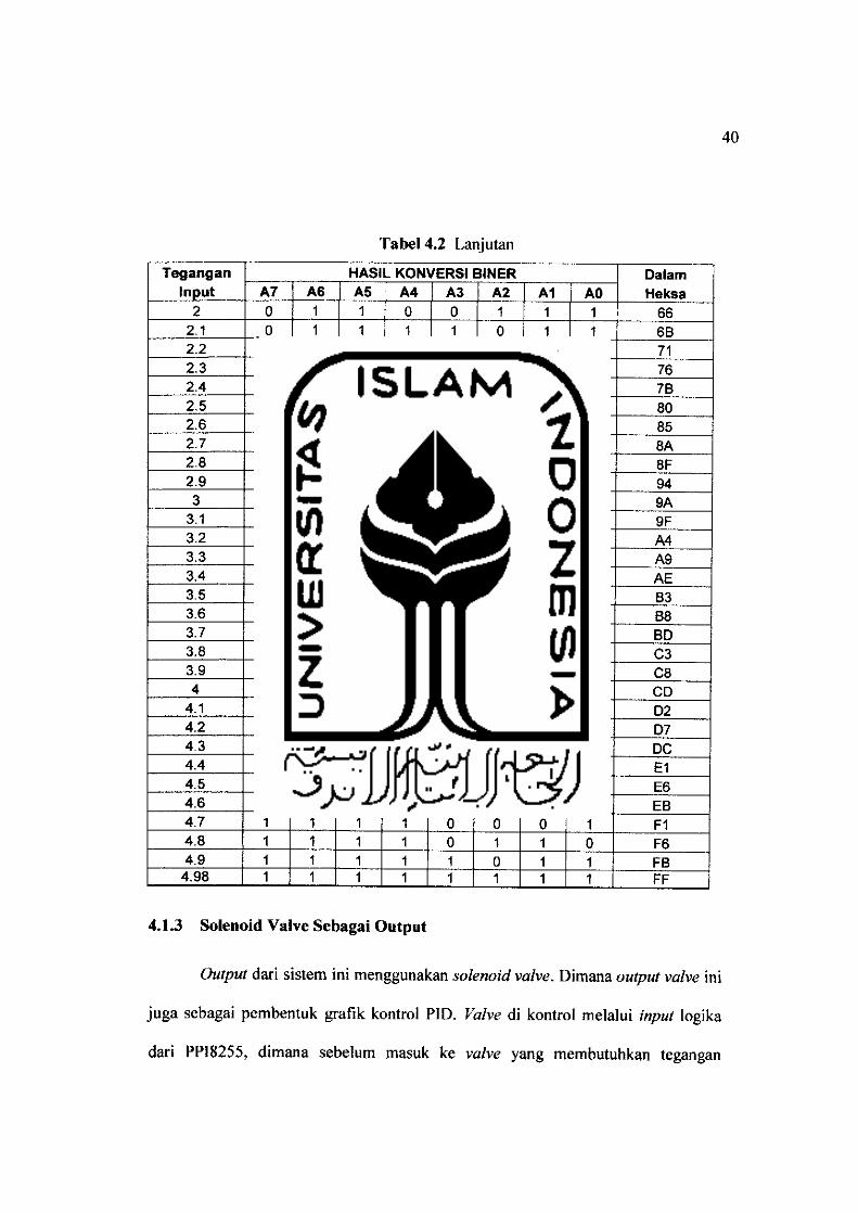
Tabel 4.2 Lanjutan
Tegangan
Input
HASIL KONVERSI BINER Dalam
HeksaA7 A6 A5 A4 A3 A2 A1 AO
2 0 0 0 1 1 1 66
2.1 0 1 1 0 1 1 6B
2.2 0 1 0 0 0 1 71
2.3 0 1 0 1 1 0 76
2.4 0 1 1 0 1 1 7B
2.5 o 0 0 0 0 0 0 80
2.6 0 0 0 0 1 0 1 85
2.7 0 0 0 1 0 1 0 8A
2.8 0 0 0 1 1 1 1 8F
2.9 0 0 1 0 1 0 0 94
3 0 0 1 1 0 1 0 9A
3.1 0 0 1 1 1 1 1 9F
3.2 0 0 0 1 0 0 A4
3.3 0 0 1 0 0 1 A9
3.4 0 0 1 1 1 0 AE
3.5 0 1 0 0 1 1 B3
3.6 0 1 1 0 0 0 B8
3.7 0 1 1 1 0 1 BD
3.8 0 0 0 0 1 1 C33.9 0 0 1 0 0 0 C8
4 0 0 1 1 0 1 CD
4.1 0 1 0 0 1 0 D2
4.2 0 1 0 1 1 1 D7
4.3 0 1 1 1 0 0 DC
4.4 0 0 0 0 1 E1
4.5 0 0 1 1 0 E6
4.6 0 1 0 1 1 EB
4.7 1 0 0 0 1 F1
4.8 1 0 1 1 0 F6
4.9 1 1 0 1 1 FB
4.98 1 1 1 1 1 FF
4.1.3 Solenoid Valve Sebagai Output
40
Output dari sistem ini menggunakan solenoid valve. Dimana output valve ini
juga sebagai pembentuk grafik kontrol PID. Valve di kontrol melalui input logika
dari PPI8255, dimana sebelum masuk ke valve yang membutuhkan tegangan

41
analog, maka bit dari PPI8255 akan di konversi menjadi tegangan oleh DAC 0808.
Valve ini memerlukan input tegangan 0-5 Volt. Sehingga ketika input logika dari
PPI8255 sebesar FFH (FF Heksa) maka DAC akan meng-konversi nya menjadi
tegangan 5 Volt. Valve akan aktif mengikuti output sistem dari kontrol PID.
4.2 Analisis Perangkat Lunak
Perangkat lunak ini menggunakan bahasa pemrograman PASCAL dengan
software Delphi 7. Sistem dibangun untuk menampilkan GUI (Graphical User
Interface) dari pemrograman kontrol PID, Gambar 4,2 ini adalah hasil dari visualisasi
perancangan pemrogramansistem kendali PIDdengan menggunakan Delphi 7.
Gambar 4.2 Tampilan GUI kontrol PID

42
Keterangan Gambar:
1. HScrolll : Merupakan input debit air yang masuk kedalam tangki visual.
Ketika tombol aktifkan pompa air di "klik" maka secara otomatis HScrolll
akan membuka penuh (100%) secara konstan sebagai masukan input. Pada
tangki yang asli pompa air akan aktif dan akan mengisi tangki secara terus
menerus dengan debit air yang konstan dan akan berhenti ketika tombol stop
pompa di "klik".
2. Tangki air visual : Ini merupakan visualisasi dari tangki air sebenamya.
Dimana ketika air terisi didalam tangki yang sebenamya maka tangki air
visual ini akan terisi juga secara otomatis. Tangki air visual ini terisi dengan
pembacaan data bit dari sensor yang telah dikonversi oleh ADC. Visual dari
tangki air ini berproses dengan sampling time 2 detik yang diatur oleh timer,
yaitu setiap 2 detik pembacaan data dari sensor maka dilakukan proses
ketinggian air yang berulang-ulang hingga batas air yang diinginkan. Proses
ketinggian air ini terbaca dalam persentase .
3. VScroIll : Digunakan sebagai pengatur ketinggian air yang diinginkan.
VScroIll ini juga merupakan setting point (SP) dari level ketinggian air.
Ketika VScroIll kita setting sebesar 50%, maka tangki air visual akan
berproses sebagai process variable yang akan mencapai nilai setting point.
Hal ini terjadi karena telah mengalami proses kontrol yang sebenamya,
dimana ketika error yang kita inginkan sama dengan nol (0) maka harus
terjadi proses dimana sesuai dengan persamaan :

E == SP -PV
Dimana,
E = Error
SP == Setting Point
PV = Process Variable
43
(4.4)
4, 5, 6. Parameter PID : Di bagian ini mempakan tempat untuk setting
parameter- parameter kontrol PID (Proporsional, Integral, Derivative) untuk
mendapatkan respon sistem yang paling baik.
7. VtChartl : Ini merupakan output grafik dari kontrol PID yang telah di setting
parameternya, Karena sistem yang dibuat ini yaitu mengontrol output
keluaran valve, maka grafik ini akan menampilkan nilai output keluaran dari
setting parameter. Grafik VtChartl ini akan berhubungan langsung dengan
Hscroll2 (no. 9) sebagai output dari sistem. Dari grafik di label Y terdapat
amplitudo yang merupakan output keluaran, sedangkan di label X mempakan
pewaktu (time) untuk mengetahui pada detik keberapa waktu proses kontrol
PID mulai terjadi.
8. Chartl : Ini mempakan grafik tegangan dari sensor potensiometer yang sudah
dikonversi oleh ADC menjadi biner. Dimana tiap bit data dari ADC akan
ditampilkan pada grafik.
9. HScroll2 : Mempakan output dari sistem yang dalam perangkat keras yang
nanti akan terhubung dengan solenoid valve sebagai keluaran air. Grafik dari

44
proses kontrol PID berawal dari bukaan HScroll2. Dimana HScrolI2 akan
sedikit demi sedikit terbuka sampai menghasilkan output respon yang baik.
HScroll2 ini dikontrol secara otomatis yang tergantung dari output sistem.
10. Panel2 : Ini digunakan sebagai penampil jam dan tanggal pada saat proses
kontrol dimulai.
11. Memo : Ini digunakan sebagai penampil proses PID yang telah terjadi dalam
perangkat lunak.
4.3 Analisis Parameter PID untuk Optimasi Level Ketinggian Air
Pengujian sistem pengaturan level ketinggian air dilakukan dengan berbagai
parameter konstanta Kp (Konstanta Proportional), Ki (Konstanta Integral), dan Kd
(Konstanta Derivative). Range pengukuran ketinggian air yang dilakukan adalah 0 -
50% yang dikonversikan oleh ADC menjadi data 0 - 255. Dalam pengujian ini data
ketinggian air yang digunakan adalah dalam skala yang ditunjukkan oleh ADC 0 -
255. Parameter yang dimasukan berbeda - beda.
4.3.1 Pengujian Sistem Kontrol PID
4.3.1.2 Pengujian Sistem Dengan Perubahan Parameter
4.3.1.2.1 Perubahan Parameter Kp

45
Tabel 4.3 Hasil Pengujian terhadap parameter Kp
SettingPoint (SP)
%
Konstanta PID Data ADC
Bit
Rise
Time
(Sec)
SteadyState
(Sec)
Over
Shoot
Error
Kp Ki Kd
30%
85 10 3 118 54.8 63 0
75 10 3 130 56.6 67 65 -2
65 10 3 148 59.8 72 67 0
55 10 3 145 59.7 72 68 -1
45 10 3 139 58.7 71 68 -5
Pada tabel percobaan diatas dapat dilihat pengaruh Kp terhadap sistem,
Pertambahan harga Kp akan menaikkan penguatan sistem sehingga dapat digunakan
untuk memperbesar kecepatan respon dan mengurangi error penyimpangan dalam
keadaan mantap (error steady state).
80
£ 60
f.40
< 20
Output Position
Ife^l'!«« *•«' <i*»TII II %A 13 14 11 Ml 17 M 14 M tl fc» a» fe* *i «« fcj t>fl
Time(sec)
Gambar 4.3 Respon output sistem dengan Kp-75, Ki=IO, Kd=3
Gambar 4,3 menunjukkan pemilihan Kp yang tidak optimal pada sistem
Pemakain alat kontrol jenis ini saja sering tidak memuaskan karena penambahan K
selain membuat sistem lebih sensitif, tetapi juga cenderung mengakibat kestabilan.

46
Disamping itu pertambahan Kp adalah terbatas dan tidak cukup untuk mencapai
respon sampai suatu harga yang diinginkan.
Kenyataan dalam usaha mengatur harga Kp terdapat keadaan-keadaan yang
bertentangan. Di satu pihak diinginkan mengurangi error sebanyak mungkin,tetapi hal
ini akan mengakibatkan osilasi bagi respons yang berarti membutuhkan waktu yang
lama pada "setting time", sedang di pihak lain respons terhadap setiap perubahan
masukan hams terjadi secepat mungkin tetapi dengan lonjakan dan osilasi sekecil
mungkin. Respons yang cepat memang dapat diperoleh dengan memperbesar Kp,
tetapi hal ini juga akan mengakibatkan ketidak stabilan sistem.
Untuk mengatasi masalah-masalah ini, alat kontrol yang akan digunakan
harus mempunyai persyaratan berikut:
a. penguatan yang tinggi pada frekuensi-frekuensi yang sangat rendah (untuk
mengurangi kesalahan-kesalahan).
b. Penguatan yang tinggi pada frekuensi-frekuensi tinggi (yakni dengan secepatnya
mengikuti perubahan masukan bila laju perubahan transien adalah yang paling
cepat). Hal ini penting untuk menjamin respon yang cepat.
c. Pada frekuensi-frekuensi menengah (yakni dalam bagian terakhir respons
transient dan sebelum "on set" (kondisi - kondisi mantap) penguatan sebaiknya
cukup rendah agar terjamin proses yang tidak mengalami lonjakan yang
berlebihan dan juga setiap kecendemngan berosilasi akan diredam dengan cepat.
4.3.1.2.2 Perubahan Parameter Ki

Tabel 4.4 Hasil Pengujian terhadap parameter Ki
SettingPoint (SP)
%
Konstanta PID
Data
ADC
Bit
Rise
Time
(Sec)
SteadyState
(Sec)
Over
Shoot
Error
Kp Ki Kd
30%
85 10 3 118 54.8 63 0
85 20 3 129 58.5 68 63 0
85 30 3 125 57.6 66 61.5 0
85 40 3 120 56.6 64 59.6 0
85 50 3 118 56.6 64 59.6 0
47
Dari tabel hasil percobaan 4.4 diatas dapat dilihat pengaruh Ki pada sebuah
sistem kontrol. Dari semua parameter Ki yang dimasukkan mengalami over shoot dan
hanya percobaan pertama pengujian terhadap parameter Ki ini. Pada dasarnya sifat
dasar kontrol Ki adalah dapat memperbaiki respon steady state, namun pemilihan Ki
yang tidak tepat atau terlalu besar dapat menyebabkan respon LJransient (transient
respon) yang tinggi sehingga dapat menyebabkan ketidakstabilan sistem. Pemilihan
Ki yang sangat tinggi justru dapat menyebabkan output berisolasi.
•g 60
•f 40-I 2C
Output Position
i- 4IJ ..: :/~.:tet: j i
• ]14t«ttll4(4tMllM It 11 II Hi I hi *3 *> *4 at •• hT h*
Time(sec)
Gambar 4.4 Respon output sistem dengan Kp-85, Ki-30, Kd=3

48
Gambar 4.4 menunjukkan respon sebuah kontrol yang tidak optimal dengan
pemilihan Ki yang besar.
4.3.1.2.3 Perubahan Parameter Kd
Tabel 4.5 Hasil Pengujian terhadap parameter Kd
Setting Point(SP)
%
Konstanta PID Data ADC
Bit
Rise
Time
(Sec)
SteadyState
(Sec)
Over
Shoot
Error
Kp Ki Kd
30%
85 10 3 118 54.8 63 0
85 10 10 118 54.8 63 _* -1
85 10 20 11855.6 64 -* -3
85 10 30 118 55.6 64 _*-5
85 10 40 118 55.6 64*
-7
Keterangan : -* => Over Shoot yang tidak kelihatan di grafik
Tabel 4.3 merupakan hasil pengujian ketika parameter Kd kita berikan nilai
bervariasi. Pada percobaan tersebut terdapat konstanta PID yang paling handal atau
ideal untuk mengatur level ketinggian air dengan settingpoint 30%. Untuk konstanta
kontrol yang paling tepat adalah dengan memasukan harga Kd - 3. Pemilihan Kd
yang tepat dapat meningkatkan stabilitas sistem, mengurangi over shoot, dan
meningkatkan respon transien. Dengan memberikan Kd yang ideal untuk tiap jenis
pengontrolan maka dapat menghasilkan respon yang cepat mencapai error. Apabila
Kd yang kita berikan teralalu besar maka stabilitas sistem akan terganggu. Pemberian

49
Kd yang kecil tidak hanya berpengaruh pada cepat nya kondisi rise time tapi juga
berpengaruh pada saat sistem mengalami steady state.
80
•» 60
= 40
< 201f
-
0 utPLIt Pa si(ic n
4 ;
j i4«4I 4*1>«1)1M(TU<1 H» 11 13 11 U » W
Time(secJ
ii i« i« kO H ft J HI U fe.l
Gambar 4.5 Respon output sistem dengan Kp-85, Ki-10, Kd=40
Gambar 4.5 menunjukkan sebuah respon output sistem yang kurang optimal denga
pemilian Kd yang besar
4.3.1.2 Pengujian Sistem dengan perubahan setting point
Setelah meiakukan percobaan dengan meiakukan perubahan pada parameter-
parameter kontrol Kp, Ki, dan Kd maka didapatkan parameter kontrol yang paling
optimal adalah Kp^85, Ki=10, dan Kd~ 3. Selanjutnya dalam pengujian ini,
dilakukan percobaan dengan parameter konstanta kontrol sama dan setting point yang
berbeda. Tujuan dari percobaan ini untuk mengetahui kehandalan pengendali PID.

50
Tabel 4.6 Hasil Pengujian terhadap settingpoint PID
SettingPoint (SP)
%
Konstanta PID Data ADC
Bit
Rise
Time
(Sec)
SteadyState
(Sec)
PV
Kp Ki Kd
30% 85 10 3 118 54.8 63 930
35% 85 10 3 126 58.8 67 1035
40% 85 10 3 141 63.6 72 1240
45% 85 10 3 153 67.6 75 1395
50% 85 10 3 168 71.9 80 1550
Pada tabel 4.6 diatas adalah hasil pengujian dengan parameter yang sama
namun dengan settingpoint yang berbeda. Hal ini dilakukan untuk mengetahui sejauh
mana parameter tersebut handal pada setiap setting point, maka dari tabel diatas
diketahui semua settingpoint pada sistem tersebut handal dengan parameter tersebut.
Nilai setting point ketinggian air 930 dan menunjukkan ketinggian air 30%
yang dilihat dari visual sedangkan di keadaan sebenamya ketinggian air 14cm.
. ™* i
IfcYAIFULWriSYURj -Outpm iooauv-f
3 jrajasi ><m n 39 33
a
Ketinggian Air -• 14 Cm
68
Proportioned gain O-l DO '
Dwrivotivw Ral* O-l 2D
Error O
I.'3
so
520
Outpur Poiltlo
-
\{
->*
Tlm«{«c)
•3 ^ejTTTFvttni
33 nrraaBi'
.a_.*:JJ.,. . W -e ' I* m ..--iivaie
Gambar 4.6 Tampilan GUI kontrol PID setelah di Run

51
Gambar 4.6 menunjukkan hasil visualisasi kontrol PID yang mulai di proses
setelah tombol aktifkan pompa air di "klik". Pada awalnya semua parameter kontrol
di setting Kp - 85, Ki = 10, dan Kd =3. Pada tangki air visual akan terjadi proses
hingga setting point yang telah di tetapkan yaitu 930 atau sebesar 30%. Pada tangki
air yang sebenamya air akan mengisi masuk hingga 14 cm. Ketika proses pengisian
padatangki air visual dan pada tangki sebenamya telah mencapai setting point maka
output sistem akan terbuka sebesar 66% dan pada solenoid valve yang telah di setting
keluarannya akan terbuka sebesar 70 Heksa yang menyesuaikan output 66% , dimana
output sistem inilah yang menjadi output dari PID.
Output Position
80 - b
-£ fin - "\3
* 40a. ^u
f 20 I
n . \« i*i 421 434 44JU 41 4B 49 SO Si 52 S3 54 51 S6 5? 5* 59 UH.1 C 2C 3 6 4 61
Time(sec)
Gambar 4.7 Respon output sistem dengan Kp-85, Ki=10, Kd-3
Pada gambar 4.4 diatas, waktu naik (rise time) terjadi pada detik ke-54,8.
Dengan memasukan harga Kp yang besar akan memperkecil overshoot dan
mempercepat pencapaian steady stale. Pencapaian steady state untuk mendapatkan
error - 0, terjadi pada detik ke- 63.

52
Untuk membuat tangki air visual dan tangki air sebenamya terkoneksi adalah
melalui data dari sensor potensiometer yang telah di konversi oleh ADC 0804. Untuk
percobaan ini kita settingpoint sebesar 930 maka tangki air sebenamya akan diisi
hingga data dari sensor terbaca 118 bit. Saat setting point yang di berikan berbeda-
bedamakadata dari sensor untuk mencapai setting point tersebut juga bervariasi. Hal
ini akan didapatkan di percobaan selanjutnya. Berikut gambar grafik dari ADC pada
percobaan pertama ini,
•I-rsM. t-.aii t-.tt.fei^i ADC C - 21~Z
1 -" 41.1 (M W. 'i.i! I >(\ -411 |^i_. U51 ,11: jiyf ^011
Gambar 4.8 Grafik ADC setelah di Run
Pada setting point selanjutnya maka diberikan masukkan nilai setting point
yang berbeda hingga 50%, maka pengaruh dari output terdapat di semua kondisi yaitu
pada data ADC, steady state, dan rise time, Semakin besar setting point yang kita
masukkan maka semakin besarpula kondisi-kondisi yang dialami sistem.
4.3.2 Pengujian Sistem Kontrol PI
Pengujian yang dilakukan dengan menggunakan kontrol PI ini untuk melihat
seberapa besar pengaruh kontrol PI terhadap sistem tanpa menambahkan kontrol D
(derivative) didalam sistem tersebut. Integral Controller memiliki karakteristik
mengurangi rise time, menambah overshoot dan selling time, serta

Wf$:fi?-ffiWY': •
Output Position
mi •
£ ©0 -
~ 40
f"
\ _.._ .-^ ....
< 20 ,
ft : ^4 *a «* 444 S«641 *»4* M « S» 13 W « MflHtlMtfUM *« «,s «c
54
Time(sec)
Gambar 4.9 Respon output sistem dengan Kp=70, Ki=8
Untuk membuat sistem stabil tanpa menambahkan kontrol Kd dipercobaan ini
maka parameter Kp haruslah lebih besar daripada parameter Ki, apabila pemilihan Ki
dan Kp tidak sesuai maka akan membuat sistem akan lambat mencapai error =0atau
bahkan akan membuat sistem sedikit berisolasi.
Pengaruh kontrol PID pada valve keluaran air adalah ketika persamaan
kontrol PID yang telah di masukkan pada sistem ini misalnya, sensor potensiometer
menghitung setiap 1detik atau lebih pendek, sehingga setiap I detik akan didapatkan
posisi kontrol valve yang bam. Error pada persamaan PID dihitung dari perbedaan
set-point dengan proses variabel. Jadi setiap I detik didapatkan error yang bam untuk
dihitung oleh PID untuk menghasilkan manipulated variabel yang baru.
Manipulated variabel (MV) - aliran airkeluaran yang diatur
Transmitter = pelampung untuk mengukur tinggi air

BABV
KESIMPULAN DAN SARAN
5.1 Kesimpulan
Dari hasil pengujian yang telah dilakukan, dapat diambil kesimpulan bahwa
sistem kontrol PID yang dibuat mampu mengontrol level ketinggian air. Secara
umum untuk aplikasi yang telah dibuat, semakin besar harga Kp maka sistem lebih
cepat mencapai steady statedan juga rise time semakin kecil. Semakin besar harga Ki
akan membuat respon sistem berisolasi dan lebih lambat mencapai keadaaan steady
state. Semakin besar harga Kd dapat membuat overshoot semakin kecil. Parameter
kontrol PID yang optimum untuk pengontrolan ketinggian air ini adalah, Kp = 80, Ki
- 10, Kd = 3 dan pada tangki air terbaca 14cm. Pada pengontrolan kontrol PI maka
parameter yang tepat di sistem ini adalah, Kp = 70, Ki - 8 dan pada tangki air terbaca
15cm.
5.2 Saran
Dari perancangan sistem yang telah direalisasikan pada Tugas Akhir ini
diharapkan dapat menjadi dasar penelitian lebih lanjut, mengingat banyaknya
keterbatasan yang dihadapi makadiusulkan beberapa saranpengembangan, yaitu :
1. Penggatian sensor dari potensiometer menjadi sensor yang lebih presisi dan
memiliki sedikit noise untuk mengukur level ketinggian air.
55

56
2. Solenoid valve yang digunakan selanjutnya lebih baik agar dapat mengukur
keluaran air dengan pasti, misalnya menggunakan motor servo sebagai
interfacing nya.
3. Pengujian sistem dengan memasukkan gangguan-gangguan yang mungkin
terjadi.
4. Memperbaiki dan membandingkan sistem dengan pengontrol Fuzzy atau
gabunagan antara Fuzzy dan PID.
5. Pada software dapat dikembangkan lagi agar dapat menganalisis ketinggian
air lebih tepat sehingga lebih sistemsecara keseluruhan akan lebih lengkap.

LAMPIRAN

S
32
.
-----
...
Ml..
17
1ff
3fi..
1a
-r
CH
JS
f__.
. 1|
+S
V
sS2
IN40
D1ik
INPU
Tlo
gic
LA
MP
IRA
N1
'+•
.2
....
.
.3
8..
.
2a
.
It
._..
(^u
na
13
j
m
+1S
v
-lc
_±
tp
5^ 1
2V
C0
1A
po
mp
sai
rJI
J?"1
>1
0k.
[5-
t^-
*_
i
3:oS
*bSe
'OU
T
ICU
V *J?
Gam
bar
Ran
gkai
anL
engk
ap
-T
15
V
-1S
VE
E
±*
IWU
12
CA
0?^
lt
-1—
®T'P
RE
LA
YS
PO
T
*ID
„M
*2
$v

// Adapted from Max Seim's BV sample [email protected] converted toDelphi5 and added a secondtype of PID algorithm.
//Andrew R Clayton 12-30-07 [email protected]
//syaiful M 2-9-2008 Cukup_ipu!J)[email protected]
unit Unit1;
interface
uses
Windows, Messages, SysUtils, Classes, Graphics, Controls, Forms, Dialogs,
StdCtrls, ExtCtrls, ComCtrls, Spin, Gauges,
Series, Chart, Buttons, SmaliPort, TeEngine, TeeProcs, OleCtrls, VCFI,
DB, DBTables;
type
TForml = class(TForm)
VScroIll :TScrollBar;
Textl:TLabeI;
StaticTextl: TStaticText;
HScroll2: TScrollBar;
GainSpinEdit: TSpinEdit;
IntregalResetSpinEdit: TSpinEdit;
DerivativeRateSpinEdit: TSpinEdit;
StaticText2: TStaticText;
StaticText3: TStaticText;
StaticText4: TStaticText;
HScrolll: TScrollBar;
Labell2:TLabel;
Label30: TLabel;
Gauge 1: TGauge;
Gauge2: TGauge;
VtChartl: TVtChart;

StaticText5: TStaticText;
Shape I: TShape;
Shape2: TShape;
Shape5: TShape;
Shape6: TShape;
Shape7: TShape;
Gauge3: TGauge;
Gauge4: TGauge;
Button2: TButton;
Chart l:TChart;
Series1: TLineSeries;
Panel 1: TPanel;
PompaAir: TButton;
Solenoid: TButton;
Editl:TEdit;
Button 1: TButton;
Panel2: TPanel;
Button3: TButton;
Memol: TMemo;
Button4: TButton;
SmaliPort l:TSmaIIPort;
Memo2: TMemo;
Button3TimerNew: TButton;
TimerNew: TTimer;
Edit2: TEdit;
Memo3: TMemo;
Memo4: TMemo;
Memo5: TMemo;
Label!: TLabel;

Label2: TLabel;
Label3: TLabel;
Label4: TLabel;
LabelTinggiAir: TLabel;
Label8: TLabel;
Panel3: TPanel;
Image 1: TImage;
procedure HScrolllChange(Sender: TObject);
procedure VScroIllChange(Sender: TObject);
procedure HScroll2Change(Sender: TObject);
procedure strobe 1;
procedure strobe2;
procedure PID(Sp,Pv:single; Var output: single);
procedure PID2(Sp,Pv:single; Var output: single);
procedure Tank();
Procedure Chart();
procedure Button2Click(Sender: TObject);
procedure FormCreate(Sender: TObject);
procedure PompaAirClick(Sender: TObject);
procedure SolenoidClick(Sender: TObject);
procedure ButtonlClick(Sender: TObject);
procedure Button3Click(Sender: TObject);
procedure Button4Click(Sender: TObject);
function CariTinggiAir(Datal: integer): integer;
procedure HitungPVAir;
procedure Edit2KeyDown(Sender: TObject; var Key: Word; Shift: TShiftState);
procedure ProsesTinggiAir(DataVisual: byte);
procedure ProsesTunda(Lama: longint);
procedureTimer]SewTimer(Sender: TObject);

procedure Button3TimerNewClick(Sender: TObject);
procedure ProsedurSolenoid(Persen: integer);
procedure BikinLabelChart(Sender: TObject);
private
{ Private declarations }
public
procedure tulis8255(port,data:byte);
{ Public declarations }
end;
const
PA-O;
PB=I;
PC=2;
PCW=3;
invalve : Single = 1.00;
outvalve : Single = LOO;
mode : integer = 1;
error : integer - 1;
supply : integer = 1;
stability : integer = I;
x : integer = 1;
y : integer = 1;
gain : single = 1.00; // Proportional Gain
reset : integer = 1; // Intregal reset
rate : integer = 1; // Derivative rate
output : single = 1.00;
PV : Single = 10.00;
si : integer= I;
s2 : integer^ I;

inputD : single- 1,00;
inputDF : single = 1.00;
inputlast: single - 1.00;
feedbackdfilter: integer = I;
feedback : Single = 1.00;
SP : integer = 1;
PV_DIV2: integer- 1550;
dfilter: integer =10;
1pt_data=$378;
lpt_status=$379;
Ipt_kontrol=$37A;
var
Forml: TForml;
wri,wrO:byte;
a,tampung:byte;
i:integer;
selesai: boolean
var TinggiAir: single;
hh, hhh: integer;
dataPort,dataVisual :byte;
chartlADC: integer;
AOwner: TComponent;
Lab: array[1..30] of TLabel;
procedure Out32(waddr:word;bOut:byte);stdcall;extemal'inpout32.dirimplementation
procedure tform LtuIis8255(port,data:byte);
begin
case port of

PA:
begin
wrl:=$08;
wr0:=$09;
end;
PB:
begin
wrl:=$0C;
wrO:=$OD;
end;
PC:
begin
wrl:=$00;
wrO:=$01;
end;
PCW:
begin
wrl:=$04;
wrO:=$05;
end;
end;
Out32($37A,wrl);
Out32($37A,wrO);
Out32($378,data);
Out32($37A,wrl);
end;
procedure de!ay(lama:longint);
var
reflongint;

begin
ref:=GetTickCount;
repeat
Application.ProcessMessages;
untiI((GetTickCount-ref)>=lama)
end;
procedure TForml.strobel;
begin
tampung:=SmallPortl.ReadByte(lpt_kontrol);
tampung:=tampung or $01;
SmallPortI.WriteByte(lpt_kontrol,tampung);
end;
procedure TForml.strobe2;
begin
tampung:^SmaIIPort1.ReadByte(lptkontrol);
tampung:=tampung and $FE;
SmallPortl.WriteByte(lpt_kontrol,tampung);
end;
{$R *.DFM}
procedure TForml.HScrolllChange(Sender: TObject);
begin
Invalve "(Hscroill.position * (supply /100))/60;
Gauge3.progress := Hscrolll.position;
If Gauge3.progress = 0 then shape5.brush.color := clwhite else
shapeS.brush.color := claqua;
If Gauge3.progress = 0 then shape2.brush.color := clwhite else
shape2.brush.color := claqua;
end;

procedure TForml.VScrolllChange(Sender: TObject);
begin
Label12.caption :=inttostr( (VScroil 1.position - (PV_DIV2 *2)));
Gauge2.progress := (PVDIV2 * 2) - VScroIll.position ;
Label 12.caption :- inttostr( (VScroIll.position - (PV_D1V2 * 2)) *-l);
sp :~ VScroIll.position;
end;
procedure TForml.HScroll2Change(Sender: TObject);
begin
Outvalve := (HScroI12.position * 30)/60 ;
Gauge4.progress := Hscrol12.position;
IfGauge4.progress = 0 then shape6.brush.color := clwhite else
shape6.brush.color := claqua;
end;
procedure TForm 1.Tank();
Begin
Gauge 1.Progress :=round(PV);
End;
Procedure TForml.Chart();
Var
Row: Integer;
temp : widestring;
Begin
VtChartl.repaint := false;
With Forml.VtChartl
Do
VtChartl.Column:=I;
VtChartl.Row := 24 ;
VtChartl.Data := inttostr(Round(100- Output));

For row := 1 to 26 Do
Begin
VtChartl.Column := 1;
VtChart 1.row :- (row +1);
temp := VtChartl.Data;
VtChart 1.row := row ;
VtChartl.Data := Temp;
Edit 1.Text:-temp;
Lab[row].Caption :- inttostr(row+hhh);
end;
VtChartl.repaint :~true;
End;
procedure TForml.PID(Sp,Pv:singIe; Varoutput: single); // no feedback
Begin
dfilter := 10;// Filter value to scale down derivative effect.
inputd := pv + (inputlast - pv) * (rate / 60); // Derivative Rate 0 to 120
inputlast := pv;
tnputdf:= inputdf+ (inputd - inputdf) * dfilter / 60 ;
output :== (sp- inputdf) * (gain /100) + feedback; // Proportional Gain
If output > 100 Then output := 100 ;//' clamp output valve between 0 and 100%
If output < 0 Then output:- 0 ;
feedback :=feedback - (feedback - output) * reset / 60; // Intregal Reset
End;
procedure TForm! .PID2(Sp,Pv:single; Varoutput: single); // no feedback
Const

ErrorLast: Single =1.00;
ErrorlastLast: Single = 1.00;
Begin
ifhhh=lthen
begin
ErrorLastLast := 1;
ErrorLast := 1;
end;
Memo4,Lines.Append('PID2- Gain ->' + floattostr(Gain));
Memo4.Lines.AppendCPID2 - Reset -> ' + floattostr(Reset));
Memo4.Lines.Append('PID2 - Rate ->' + floattostr(Rate));
Memo4.Lines.AppendCPID2 - Error ->' + floattostr(Error));
Memo4.Lines.Append(PID2 •ErrorLast -> ' + floattostr(ErrorLast));
Memo4.Lines.Append('PID2 - ErrorLastLast -> ' + floattostr(ErTorLastLast));
output := Output + (Gain/100) * (Error - ErrorLast + (Reset / 60)* Error + (Rate/60) *(error- ErrorLast* 2 + ErrorLastLast));
ErrorLastLast := ErrorLast;
ErrorLast := Error;
If output > 100Then output := 100;//" clampoutput valve between 0 and 100%
If output < 0 Then output := 0 ;
End;
procedure TForml.Button2Click(Sender: TObject);
begin
selesai:=true;
tulis8255(PC,$00);
tulis8255(PB,$00);
Shape 1.Brush.Co!or:=clwhite;
HScrolll.Position:=0;
HScroll2.Position:^ 0;

end;
procedure TForml.FormCreate(Sender: TObject);
var Shift: TShiftState;
Key: word;
x: integer;
begin
tulis8255(PCW,$80);
tulis8255(PB,$FF);
tu!is8255(PC,$00);
tulis8255(PA,$flf);
HScroll2.Position:=0;
Textl.Caption:=";
VScroil 1.Max := PV_DIV2 * 2;
Gauge2.MaxValue := PV_DIV2 * 2;
Gauge I.MaxValue := PV_DIV2 * 2;
BikinLabelChart(Sender);
Edit2.Text:= '255';
Key:=13;
Edit2KeyDown(Sender, Key, Shift);
for x := 1 to 26 do
Lab[x].Caption:- inttostr(x);
Gauge1.Progress :=0;
Edit2.CIear;
end;
procedure TForml.PompaAirClick(Sender: TObject);
var
dd: TDateTime;
tt: TTime;
begin

tulis8255(PB,$00);
TimerNew.Enabled := true;
chart 1ADC :=0;
dd := Date;
tt := Time;
Memo2.Lines.Append(Caption + ' - Mulai');
Memo2.Lines.Append('SP PV Output lOO-Output invalve outvalve');
Memo 1.Lines.Append(");
Memol.Lines.Append(DateToStr(dd) + " + TimeToStr(tt));
Memol.Lines.Append('MENGISI TANGKI');
begin
Labell2.Caption :- inttostr(VScroil I. Position);
supply :=2000;
HScrolll.Position:=100;
invalve := (HScrolll.Position * (supply / 100)) / 60 ;
outvalve := 0;
Textl.Caption := inttostr(Round( (PV_DIV2 * 2) -pv));
mode := 1;
HScrolI2.Enabled := true;
gain := GainSpinedit.value;
reset := IntregalResetSpinedit.value;
rate := DerivativeRateSpinedit.value;
Label 12.Caption := inttostr( VScroIll.Position);
sp := VScroil I.Position;
Shape2.Brush.Color:=clAqua;
Shapel .Brush.Color:=clAqua;
selesai:=false;
Series 1.Clear;

end;
end;
procedure TFormI.SolenoidClick(Sender: TObject);
begin
tulis8255(PC,$00);
tulis8255(PA,$64);
end;
procedure TForml.ButtonlCIick(Sender: TObject);
var
Nm: string;
dd: TDateTime;
tt: TTime;
begin
dd := Date;
tt := Time;
Nm ~ DateToStr(dd) +' *+ TimeToStr(tt);
Memo 1.Lines.Append(");
Memo 1.Lines.Append(DateToStr(dd) + " + TimeToStr(tt));
tulis8255(PC,$flf);
tulis8255(PA,$00);
Application.Terminate;
end;
procedure TForm LButton3Click(Sender: TObject);
begin
tu!is8255(PB,$FF);
end;
procedure TForm LButton4CIick(Sender: TObject);
begin
Memol.Lines. Append(");

Memol.Lines.Append('MENGOSONGKAN TANGKI');
Memo2.Lines. Append(");
Memo2. Lines.AppendCMENGOSONGKAN TANGKI');
tulis8255(PC,$00);
tulis8255(PA,$64);
end;
function TForm I,CariTinggiAir(Datal: integer):integer;
var Hasil: integer;
begin
Hasil :=0;
f (Datal >= 6) and (Datal <= 13) then Hasil := 0;
f(Datal >= 14)and (Datal <= 21) then Hasil :=I ;
f (Datal >= 22) and (Datal <= 30) then Hasil := 2;
f (Datal >= 31) and (Datal <= 38) then Hasil := 3;
f (Datal >= 39) and (Datal <^ 45) then Hasil := 4;
f (Datal >= 46) and (Datal <= 52) then Hasil —5;
f (Datal >= 53) and (Datal <= 60) then Hasil := 6;
f (Datal >= 61) and (Datal <= 67) then Hasil := 7;
f (Datal >= 68) and (Datal <= 74) then Hasil ~ 8;
f (Datal >= 75) and (Datal <= 81) then Hasil := 9;
f (Datal >= 82) and (Datal <= 89) then Hasil := 10;
f (Data! >= 90) and (Datal <= 97) then Hasil := 11;
f (Datal >= 98) and (Datal <== 104) then Hasil := 12;
f (Datal >= 105) and (Datal <= 111) then Hasil := 13;
f (Datal >= 112) and (Datal <= 118) then Hasil := 14;
f (Datal >= 119) and (Datal <= 126) then Hasil := 15;
f (Datal >= 127) and (Datal <= 134) then Hasil := 16;
f (Datal >= 135) and (Datal <= 143) then Hasil :- 17;
f (Datal >= 144) and (Datal <== 151) then Hasil " 18;

if (Datal >= 152) and (Datal <= 159) then Hasii := 19;
if (Datal >= 160) and (Datal <= 166) then Hasil := 20;
if (Datal >= 167) and (Datal <= 176) then Hasil := 21;
if (Datal >= 181) and (Datal <= 187) then Hasil := 22;
if (Datal >= 188) and (Datal <= 196) then Hasil :=23;
if (Datal >= 197) and (Datal <= 205) then Hasil := 24;
if (Datal >= 206) and (Datal <= 214) then Hasil := 25;
if (Datal >= 215) and (Datal <= 222) then Hasil ~ 26;
if (Datal >= 223) and (Datal <= 229) then Hasil := 27;
if (Datal >= 230) and (Datal <= 238) then Hasil := 28;
if (Datal >= 239) and (Datal <= 247) then Hasil := 29;
if (Datal >= 248) and (Datal <= 255) then Hasil := 30;
Result .= hasil;
end;
// BARU 23-FEB-2009
procedure TForml.Edit2KeyDown(Sender: TObject; var Key: Word;
Shift: TShiftState);
begin
ifKey=13then
begin
dataPort := strtoint(edit2.Text);
case dataPort of
0 : begin
Gaugel.Progress := 0;
dataVisual := 0;
end;
244..255:
dataVisual :=8I;
else

dataVisual := (dataPort) div 3;
end;
Label2.Caption := IntToStr(dataPort); // DataPort Asli
Label4.Caption := IntToStr(dataVisual); // DataPort Visual
ProsesTinggiAir(DataVisual);
// Ketinggian Air
LabelTinggiAir.Caption := 'Ketinggian Air=' + IntToStr(CariTinggiAir(dataPort)) + *Cm';
// Grafik ADC
with Chart1 do
with Series 1 do
addxy(chart 1ADC,dataPort,",clBlue);
inc(chartlADC);
ProsedurSolenoid(error);
end;
end;
procedure TForml.HitungPVAir;
Const
Toggle : boolean = false;
begin
//16-02-2009 23-15-15
hhh:=hhh + l;
Toggle := not toggle;
sp := (PV_DIV2 * 2) - VScroil 1.Position;
Gain := GainSpinEdit. value; //0 to 100
Reset := IntregalResetSpinEdit.value; // 0 to 120 sees
Rate :- DerivativeRateSpinEdit.value; // 0 to 120 sees
If pv <(PV_DIV2 *2) Then pv := pv +invalve ; // add and subtract product to tank x*^^OgT
!i;ll,?-,,,|ii \'ijJ.L;j.!.:l"!;i\PEF1

If pv > 0 Then pv := pv - outvalve;
Textl.Caption := IntToStr(Round( pv));
error:- round(sp - pv);
Memo4.Lines.Append('Pv -> ' + floattostr(pv));
Memo4.Lines.Append('error -> ' + floattostr(error));
Label30.Caption :— inttostiferror);
PID2(Sp,Pv, output); // feedback
HScroll2.Position := 100 - round (output);//' Change slider value (AUTO MODE)
Memo4.Lines.Append('HitungAirAqua - HScroll2.Position -> ' +inttostr(HScroI12.Position));
Tank();
If not toggle then Chart(); // reduce flicker
Memo3Lines.Append(inttostr(hhh) +' ' +floattostr(Sp) +* ' +floattostr(Pv) +' ' +floattosttfOutput)+ ' M-floattostr(100-Output) + ' ' + floattostr(inva!ve) +* ' + tloattostr(outvalve));
Memo4.Lines.Append(inttostr(hhh) +' ' + floattostr(output) +' ' + floattostr(invalve) +' ' +floattostr(outvalve) + ' ' + mttostr(en-or) +' ' + inttostr(supply) +' ' + floattostr(gain) + ' ' +inttostr(reset) +' ' + floattostr(rate) +' ' + floattostr(PV) + ' ' + floattostr(inputD) + ' ' +fioattostr(inputDF) +' ' + floattostifinputlast) +' ' +floattostr(feedback) +' ' + inttostr(SP) +' ' +inttostr(dfilter) + ' ' + inttostr(HScroin.position)+ ' ' + inttostr(HScroll2.position) +' ' +inttostr(VScroil 1.position));
Memo4. Lines. Append(");
end;
procedure TForml.ProsesTinggiAir(DataVisual: byte);
var u: byte;
begin
Memo4.C!ear;
Memo3.Clear;
HScroll2.Enabled := true;
HScrolll.Position:=100;
supply := 2000;
invalve := (HScroll1.Position * (supply / 100)) / 60 ;

outvalve := 0 ;
gain := GainSpinedit.value;
reset := IntregalResetSpinedit.value;
rate :~ DerivativeRateSpinedit.value;
sp := VScrolIl.Position;
hhh ~0;
HScroll2.Position:=0;
PV :=1.00;
output := LOO;
inputD := 1.00;
inputDF -1.00;
inputlast := 1.00;
feedback := 1.00;
for u := 1 to DataVisual do
begin
HitungPVAir;
ProsesTunda(30000);
end;
end;
procedure TForml.ProsesTunda(Lama: longint);
var u: longint;
begin
for u := 1 to Lama do
begin
Application.ProcessMessages;
end;
end;
procedure TForml.TimerNewTimer(Sender: TObject);
begin

Panel2.Caption := DateTimeToStr(now) ;
TimerNew.Enabled := false;
strobe1;
a~SmallPortl .ReadByte(lpt_status)and $F0;
a:=a shr 4;
strobe2;
a:=a or (SmallPortLReadByte(lpt__status) and $F0);
dataPort:=a xor $88;
// coz: saat DataPort 81, nilai PV sudah 1550
// padahal PV 1550 harusnya DataPort 255, maka 255 / 81 = 3.148
case dataPort of
244..255:
dataVisual :=81;
else
dataVisual := (dataPort) div 3;
end;
Label2.Caption := IntToStr(dataPort); // DataPort Asli
LabeM.Caption := IntToStr(dataVisual); // DataPort Visual
edit2.Text := inttostr(dataPort);
ProsesTinggiAir(DataVisuaI);
ProsesTunda(50000);
//Ketinggian Air
LabelTinggiAir.Caption := 'Ketinggian Air = ' + IntToStr(CariTinggiAir(dataPort)) + ' Cm';
// Grafik ADC
Panel 1.Caption—JntToStr(dataPort);
with Chart 1 doo
with Series 1 do
addxy(chartlADC,dataPort,",clBlue);
inc(chartlADC);

// ProsedurSolenoid
ProsedurSolenoid(error);
TimerNew.Enabled := true;
end;
procedure TForm LButton3TimerNewClick(Sender: TObject);
begin
TimerNew.Enabled := not TimerNew.Enabled;
end;
procedure TForml.ProsedurSolenoid(Persen: integer);
var heksa: byte;
begin
case Persen of
0 : heksa := $00;
1..1549: heksa :=$ff;
end;
Label8.Caption := IntToStr(Persen) +' %';
tulis8255(PC,$00);
tulis8255(PA,heksa);
end;
procedure TForml.BikinLabelChart(Sender: TObject);
var x: integer;
begin
for x := 1 to 26 do
begin
Lab[xj :=TLabel.Create(AOwner);
Lab[xl.Parent:=Panel3;
Lab[x].Font.Name := 'MS Serif;
Lab[x].Font.Size :=6;
Lab[x].Top :~ 0;

ifx= 1 then
Lab[x].Left:=86//102
else
begin
case x of
1..10 : Labfxl-Left := Lab[x-l].Left + 13;
11.. 15 :Lab[x].Left
16..20:Lab[x].Left
2L.30 : Lab[x].Left
end;
end;
end;
end;
end.
= Lab[x-l].Left + 17
= Lab[x-l].Left + 15
-Lab[x-l].Left + 15

& National SemiconductorMay 1999
OAC0808
8-Bit D/A Converter
General DescriptionThe DAC0808 is an 8-bit monolithic digital-to-analog converter (DAC) featuring a full scale output current settling timeof 150 ns while dissipating only 33 mW with ±5V supplies.No reference current (fREF) trimming is required for mostapplications since the full scale output current is typically ±1LSB of 255 lpjrp/256. Relative accuracies of better than±0.19% assure 9-bit monotonicity and linearity while zerolevel output current of less than 4 uA provides 8-bit zeroaccuracy for lREF>2 mA. The power supply currents of theDAC0808 is independent of bit codes, and exhibits essentially constant device characteristics over the entire supplyvoltage range.
The DAC0808 will interface directly with popular TTL, DTL orCMOS logic levels, and is a direct replacement for theMC1508/MC1408. For higher speed applications, seeDAC0800 data sheet.
Features• Relative accuracy: ±0.19% error maximum• Full scale current match: ±1 LSB typ• Fast settling time: 150 ns typ• Noninverting digital inputs are TTL and CMOS
compatible
• High speed multiplying input slew rate: 8 mA/us• Power supply voltage range: ±4.5V to ±18V• Low power consumption: 33 mW @ ±5V
Block and Connection Diagrams
W«fF|.)0-
*REF|-)0-
*l « M M If At »7 M
CURRENT MlTGWS
iiinni
5REFCREMCiCURRENT MH>
Nf* GUM HITSOURCE MIR
*K
Dual-Jn-Line Package
« {MOTE1) — u 16— COMPENSATION
GND —
MSI At —
DRCMH
«-i ^«1
Al i«
M — J-«
DS005687-2
Top ViewOrder Number DAC0608
See NS Package M16A or N16A
>2Q01 National Semiconductor Corporation DS005687 www.national.com
5oo00o00
oo
00
a
?oo3<CD
CD

COo00o
o
§
Block and Connection Diagrams (Continued)
Ordering Information
ACCURACY
Small-Outline Package
¥cc"" 1 16 -AB tSB
%-(♦}- 2 15 -A7
vWFH- i 14 —A«
CQMPMSATIOK- * II -A5
NC {NOTE 2)- 5 1! -A+
GND- e 11 -A3
VEE- 7 10 -A2
10— a 9 —A1 USB
OPERATING
TEMPERATURE RANGE N PACKAGE (N16A)
(Note 1)
8-bit 0*C<Td<+75'C DAC0808LCN MC1408P8
Note 1: Devices may be ordered by using eithef oftfer number.
www.nalional.com
SO PACKAGE
(M16A)
DAC0808LCM

s
No
the
No;
Nof
afe
pacjNot
Not
Hot
Noti
Absolute Maximum Ratings (Note 2)If Military/Aerospace specrfied devices are required,please contact the National Semiconductor Sales Office/Distributors for availability and specifications.
Power Supply Voltage
VCc
Digital Input Voltage, V5-V12
Applied Output Voltage, V0
Reference Current, l14
Reference Amplifier Inputs, V14, V15
Power Dissipation (Note 4)
ESD Susceptibility (Note 5)
+18 VDC-18 V^
-lOVoctO+ISV^
-11 VDCto+18VDC5 mA
Vcc VEE1000 mW
TBD
Storage Temperature RangeLead Temp. (Soldering, 10 seconds)
Dual-ln-Line Package (Plastic)Dual-ln-Line Package (Ceramic)Surface Mount Package
Vapor Phase (60 seconds)
fnfrared (15 seconds)
Operating RatingsTemperature Range
DAC0808
-65'Cto +150"C
260'C
300'C
215'C
220'C
' MIN ^ TA £ TMAX
0 <TA < +75"C
Electrical Characteristics(vcc = 5V. vee = ~15 vdc' vref^R14 = 2 mA, and all digital inputs at high logic fevel unless otherwise noted.)Symbol
TyEr
tpLH> 'F
TCIo
MSB
Vih
viSB
Typ
LogidInput
£ U
www. national.
Parameter
Relative Accuracy (Error Relative
to Full Scale l0)
DAC0808LC (LM1408-8)
Settling Time to Within V6 LSB
(Includes tpLH)
Propagation Delay Time
Output Full Scale Current Drift
Digital Input Logic Levels
High Level, Logic "1"
Low Level, Logic "0"
Digital Input Current
High Level
Low Level
Reference Input Bias Current
Output Current Range
Output Current
Output Current, All Bits Low
Output Voltage Compliance (Note 3)
VEE=-5V, lREF=1 mA
VP(= Below -10V
Reference Current Slew Rate
Output Current Power Supply
Sensitivity
Power Supply Current (All Bits
Low)
Power Supply Voltage Range
Power Dissipation
Conditions
(Figure 4)
TA=25°C (Note 7),
(Figure 5)
TA = 25"C, (Figure 5)
(Figure 3)
(Figure 3)
VIH = 5V
VIL = 0.8V
(Figure 3)
(Figure 3)
VeE = -5V
VEE = -15V, TA = 25*C
VREF = 2.000V,
R14 = 100QH.
(Figure 3)
(Figure 3)
Ers0.19%, TA = 25'C
(Figure 6)
-5V £ Vec £-16.5V
(Figure 3}
TA - 25'C, (Figure 3)
Min
1.9
4.5
-4.5
Typ
150
30
±20
0
-0.003
-1
2.0
2.0
1.99
0
0.05
2.3
-4.3
5.0
-15
Max
±0.19
100
0.8
0.040
-0.8
-3
2.1
4.2
2.1
4
-0.55, +0.4
-5.0, +0.4
2.7
22
-13
5.5
-16.5
Units
%
%
ns
ppnVC
mA
mA
pA
mA
mA
mA
MA
mA/us
uA/V
mA
mA
www. nattona!.com
D>a©COo00

Typical Performance Characteristics vcc *sv, vEE =-isv, ta =25 c unless otherwisenoted (Continued)
Output Current vs OutputVoltage (Output VoltageCompliance)
2.HALL BITS "ON" 1
2.4
2
1 1 |1 1
VEE «-16V V££ •-5V
r 1 <14 c?"iA1.6 1 j
l.Z I14 E 1 mA
0.8 MT —Ll_
0.4 ll4=ft2mA
0 JT 1 1 1-14 -ID -6-2 Z B 10 14 IB
Vq - OUTPUT VOLTAGE (V)
DSOQSS87-17
Typical Power SupplyCurrent vs VEE
ALL BITS HIGH OR LOWi 1 1 1 1lEEWtTHI14.2m*
- lEt WITHlM-1mA" —
lEEWITH 1,4 »0^mA
^ "I i'«
0-1-4-6 -8-IO-12-I4-1B-1I-20
VEE - NE6AT1VEPOWER SUPPLY|V(
DS0O5687-3O
Output Voltage Compliancevs Temperature
SHADEDAREA INDICATES!
PERMISSIBLE OUTPUT
VOLTAGE RANGE FOR
VEE'-ISVJH-ZnA
0 50 100
TEMPERATURE IT)
Typical Power SupplyCurrent vs Vcc
A
1LL
4*
ITSHIG ^0RL( W
j' E
' C
0 2 4 8 8 10 12 14 IS IB 20
VCc " POSITIVE POWER SUPPLY <V)
DS0056B7-2I DS005687-22
Unless otherwise specified; R14 = R15 = 1 kii, C= 15 pF, pin 16 to VEE; RL =50Q. pin 4 to ground.Curve A: Large Signal Bandwidth Method ofFigure 7 VREF =2 Vp-p offset 1V above ground.Curve B: Small Signal Bandwidth Method of Figure 7, RL =250Q, VREF =50 mVp-p offset 200 mV above ground.Curve C: Large and Small Signal Bandwidth Method of Figure 9(no op amp, RL =50fl), Rs =50Q, VRFF =2V V* =100 mVD-Dcentered at OV. ' s w w
Typical Power SupplyCurrent vs Temperature
8.0
7.D
6.0
S.D
4.0
3.0
2.0
1.0
0
ALL BITS HIGH OR LOW
-SO 0 SO 100
TEMPERATURE TCI
Reference InputFrequency Response
E
4
2
0
-2
-4
-6
-8
-10
-12
-14
-16
0.1
S B
A -
CV
0.3 1 ]
f-FREQUENCY (MHz)
(50
www. n a lio naI.com
a>
©00a00

DA
C0
80
8
"K
r~
sz
6
%if
O-*
y^
sask
ifto
te
5V
^V
•\a
e—
e<
—vw
•W
r--
VV
V-
-w
v
v«
FIGU
RE2.
Equi
vale
ntC
ircui
toft
heDA
C0B0
8Se
ries
(Not
e8)

Test Circuits
OS005687-6
V| and \-\ apply to inputs A1-A8.
The resistor tied lo pin 15 isto temperature compensate the bias current and may not be necessary for all applications.
h=̂ (~ +~^~+^+̂ : +̂ +~ +A2-A2+A£ + ;A6 + A6_A7A88 16 32 64 128 256
VrefR14
where K
and A^ = "1" tfAmis at high levelAm = "0" if An is at low level
FIGURE 3. Notation Definitions Test Circuit (Note 8)
"Ti.
FIGURE 4. Relative Accuracy Test Circuit (Note 8)
www.national.com
D>Oo00oCO

COo00o
o<
Test CirCUitS (Continued)
'© l»
www.national.com
iii.' o
ivDC
•o—Wv-
15 " :,.T"FOR IE RUNS TIME
MEASUREMENT lAlt 1111SWITCHED LOW ID HIGH)
IETTLMS IIM
t,[FICVRCi) Vto *w lm
X
1.1 4.F
r-r°l
**«
FIGURE 5. Transient Response and Settling Time (Note 8)
vCc
Zo-JZlo,*, "ZTL.15 . '1
DACM08
SCOPE
SLEWING
TIME
dl 1 dV
dt Hl dt
DS0056B7-9
FIGURE 6. Reference Current Slew Rate Measurement (Note 8)
A1
A2_
ajo-I
9ASO—
10Aer>-
A.""
Vcc
DAC0WH
R14-R1S
iSo-Jdo-R14
15 _ .HIS
2
—o-
-JsEfI SEE TEXT FOR VALUESOF C
VEEOS005687-10
FIGURE 7. Positive VRCF (Note 8}
\
r*L-«nmTO

Test Circuits (Continued)
flU^RIS
SEE TEXT FOR VALUES OF C
FIGURE 8. Negative VREF (Note 8)
vS
f~}jfISf5
A1
VfiEF
When VS = 0, h4 = 2.0 mA
^ V°fe*£l(*K
|(-Ov0
FIGURE 9. Programmable Gain Amplifier orDigital Attenuator Circuit (Note 8)
Application Hints
REFERENCE AMPLIFIER DRIVE AND COMPENSATION
The reference amplifier provides a voltage at pin 14 forconverting the reference voltage to a current, and a^um-around circuit or current mirror for feeding the ladder,rhe reference amplifier input currrent, l14, must always flownto pin 14, regardless of the set-up method or reference/oltage polarity.
Connections for a positive voltage are shown in Figure 7."he reference voltage source supplies the full current lT4.
For bipolar reference signals, as tn the multiplying mode,R15 can be tied to a negative voltage corresponding to theminimum input level. Itis possibleto eliminate R15with onlya small sacrifice in accuracy and temperature drift.
The compensation capacitor value must be increased withincreases in R14 to maintain properphase margin; for R14values of 1, 2.5 and 5k£i, minimumcapacitor values are 15,37 and 75 pF. The capacitor may be tied to either VEe orground, but using VEE increases negative supply rejection.A negative reference voltage may be used if R14 isgrounded and the reference voltage is applied to R15 asshown in Figure 8. A high input impedance is the main
www.national.com
OCOoCO

COoCOo
o<
Application Hints (continued)advantage of this method. Compensation involves a capacitor to VEE on pin 16, using the values of the previousparagraph. The negative reference voltage must be at least4V above the VEE supply. Bipolar input signals may behandled by connecting R14 to a positive reference voltageequal to the peak positive input level at pin 15.
When a DC reference voltage is used, capacitive bypass toground is recommended. The 5V logic supply is not recommended as a reference voltage. Ifa well regulated 5V supplywhich drives logic is to be used as the reference, R14 shouldbe decoupled by connecting it to 5V through another resistorand bypassing the junction of the 2 resistors with 0.1 uF toground. For reference voltages greater than 5V, a clampdiode is recommended between pin 14 and ground.
If pin 14 is driven by a high impedance such as a transistorcurrent source, none of the above compensation methodsapply and the amplifier must be heavily compensated, decreasing the overall bandwidth.
OUTPUT VOLTAGE RANGE
The voltage on pin 4 is restricted to a range of -0.55 to 0.4Vwhen VEE = ~5V due to the current switching methodsemployed in the DAC0808.
The negative output voltage compliance of the DAC0808 isextended to -5V where the negative supply voltage is morenegative than -10V. Using a full-scale current of 1.992 mAand load resistor of 2.5 kI2 between pin 4 and ground willyield a voltage output of 256 levels between 0 and -4.980V.Floating pin 1 does not affect the converter speed or powerdissipation. However, the value of the toad resistor determines the switching time due to increased voltage swing.Values of Rl up to 50011 do not significantly affect performance, but a 2.5 kli toad increases worst-case settling timeto 1.2 us (when all bits are switched ON). Refer to thesubsequent text section on Settling Time for more details onoutput loading.
OUTPUT CURRENT RANGE
The output current maximum rating of 4.2 mA may be usedonly for negative supply voltages more negative than -8V,due to the increased voltage drop across the resistors in thereference current amplifier.
ACCURACY
Absolute accuracy is the measure of each output currentlevel with respect to its intended value, and is dependentupon relative accuracy and full-scale current drift. Relativeaccuracy is the measure of each output current level as afraction of the full-scale current The relative accuracy of theDAC0808 is essentially constant with temperature due to theexcellent temperature tracking of the monolithic resistor lad
www. national.com 10
der. The reference current may drift with temperature, causing a change in the absolute accuracy of output currentHowever, the DAC0808 has a very low full-scale current driftwith temperature.
The DAC0808 series is guaranteed accurate to within ±VSLSB at a full-scale output current of 1.992 mA. This corresponds to a reference amplifier output current drive to theladder network of 2 mA,with the toss of 1 LSB(8 uA)whictiis the ladder remainder shunted to ground. The input cunerctto pin 14 has a guaranteed value of between 1.9 and 2.1 mA,allowing some mismatch in the NPN current source pair. Theaccuracy test circuit is shown in Figure 4. The 12-bit converter is calibrated for a full-scale output current of 1.992mA. This is an optional step since the DAC0808 accuracy isessentially the same between 1.5 and 2.5 mA. Then theDAC0808 circuits' full-scale current is trimmed to the same
value with R14 so that a zero value appears at the erroramplifier output. The counter is activated and the error bandmay be displayed on an oscilloscope, detected by comparators, or stored in a peak detector.
Two 8-bit D-to-A converters may not be used to construct a16-bit accuracy D-to-A converter. 16-bit accuracy implies atotal error of ±Vz of one part in 65,536 or ±0.00076%, whichis much more accurate than the ±0.019% specification provided by the DAC0808.
MULTIPLYING ACCURACY
The DAC0808 may be used in the multiplying mode with8-bit accuracy when the reference current is varied over arange of 256:1. If the reference current in the muttipfyingmode ranges from 16 uA to 4 mA, the additional errorcontributions are less than 1.6 pA This is well within 8-bitaccuracy when referred to full-scale.
A monotonic converter is one which supplies an increase incurrent for each increment in the binary word. Typically, theDAC0808 is monotonic for all values of reference currentabove 0.5 mA. The recommended range for operation with aDC reference current is 0.5 to 4 mA.
SETTLING TIME
The worst-case switching condition occurs when all bits areswitched ON, which corresponds to a low-to-high transitionfor alt bits. This time is typically 150 ns for settling to within±V£ LSB, for 8-bit accuracy, and 100 ns to V£ LSB for 7 and6-bit accuracy. The turn OFF is typically under 100 ns. Thesetimes apply when f\ <, 500i2 and C0 < 25 pF.
Extra care must be taken in board layout since this is usuallythe dominant factor in satisfactory test results when measuring settling time. Short leads, 100 pF supply bypassing forlow frequencies, and minimum scope lead length are allmandatory.

Physical Dimensions inches (millimeters) unless otherwise noted
P.010-II.0ZB
(D.2M- fl.MI)
13.910-3.988) t" '̂
r B* MAX TYP
ALL LEADS
11.388-0.394
(9 804-10.00)
IS 15 H 13 V 11 10 9
fl fl ft ft Q a Q fl
UU UUUOkli,1 J 3 4 S 6 7
(0.?M)
0.004-0.010
:«£ ^ LT
0.0W-0.010
[0.?03-0!54|TYP ALL LEADS
95°±5'
0.004
(0.102)ALL LEU TIPS
(0.408-1.ITD)TYP ALL LEADS
Small Outline PackageOrder Number DAC0808LCM
NS Package Number M16A
0.843-0470
(21.41-22.ID)
©UWUILillillillZlliJ
0.040
(L016J-TYP
(0103)
0.250 +0.005
(6.350 ±0.127)
_1
0.130 ±0.MS
(3.302 ±0.127)
WiYimr^w0.145-0.200
_£ (3J83-5.M0)
0.011 ±8.803 0.125-0.140 (0JJ"(0.457 ±0.0761 (3-175-3.556)
(2.540 +0.254)
DuaNn-Line PackageOrder Number DAC0808
NS Package Number N16A
www. n ation al.com
O>Oo00o00

a>
r
>co
a
Q
CQ•
oo
ooo00o
O
2
Notes
LIFE SUPPORT POLICY
^w!2^S PRODUCTS ARE NOT AUTHORIZED FOR USE AS CRITICAL COMPONENTS IN LIFE SUPPORT
1. Life support devices or systems are devices orsystems which, (a) are intended for surgical implantinto the body, or (b) support or sustain life, andwhose failure to perform when properly used inaccordance with instructions for use provided in thelabeling, can be reasonably expected to result in asignificant injury to the user.
<*National SemiconductorCorporationAmericas
Email: [email protected]
www.national.com
National SemiconductorEurope
Fax: +49 (0) 180-530 85 86Email: [email protected]
Deutsch Tel: +49(0)69 9508 6208English Tel: +44 (0) 870 24 0 2171Francais Tel. +33 (0) 1 41 91 8790
2. A critical component is any component of a lifesupport device or system whose failure to performcan be reasonably expected to cause the failure ofthe life support device or system, or to affect itssafety or effectiveness.
National SamlconductorAsla Pacific: CustomerResponse GroupTal: 65-2544466
Fax: 65-2504466
Email: [email protected]
National SemiconductorJapan Ltd.
Tel: 81-3-5639-7560
Fax: 81-3-5639-7507
NM do* no. a*™ any ^s%fc, u* o, any d™*ry d^d, no aror* p** I™ mm^*nd Nrfonl ma^s l» ngh, a, any^f£^^^m^^snd sp6df^Vom
•74

intefsil®
Data Sheet
8-Bit, Microprocessor-Compatible, AIDConverters
The ADC080X family are CMOS 8-Bit, successive-approximation A/D converters which use a modifiedpotentiometric ladder and are designed to operate with the8080A control bus via three-state outputs. These converters
appear to the processor as memory locations or I/O ports,and hence no interfacing logic is required.
The differential analog voltage input has good common-mode-rejection and permits offsetting the analog zerc-input-vottage value. In addition, the voltage reference input can beadjusted to allow encoding any smaller analog voltage spanto the full 8 bits of resolution.
Typical Application Schematic
i+6V l50pF
i*rM
1 MFF ,l_^ /INPUTS
LoVref^I
/7777
8-BIT RESOLUTION 1OVER ANY
DESIRED
ANALOG INPUT
VOLTAGE RANGE
Ordering Information
ADC0803, ADC0804
August 2002 FN3094.4
Features
• 80C48 and 80C80/85 Bus Compatible- No InterfacingLogic Required
• Conversion Time <100u.s
• Easy Interface to Most Microprocessors
• Will Operate in a "Stand Alone" Mode
• Differential Analog Voltage Inputs
• Works with Bandgap Voltage References
• TTL Compatible Inputs and Outputs
• On-Chip Clock Generator
• Analog Voltage Input Range(Single + 5V Supply) 0V to 5V
• No Zero-Adjust Required
• 80C48 and 80C80/85 Bus Compatible - No InterfacingLogicRequired
Pinout
&.DC0803, ADC0804
(PDIP)
TOP VIEW
csfT \J 2J)jV+ORVREFRD[2 T5JCLKRWRL£ «| DBo (LSB)
CLK IN \X rFJDB,INTR [6 I^DB;
vin(+)H lS|DBjVin (-) Q «1DB4AGND[8 ISJDBs
vREF« rj[ I^DBeDGND Qo HI DB7 (MSB)
PART NUMBER ERROR EXTERNAL CONDITIONS TEMP. RANGE(°C) PACKAGE PKG. NO
ADC0803LCN ±1/2 LSB VREF/2 Adjusted for Correct Full ScaleReading
0to70 20 Ld PDIP E20.3
f\DC08Q4LCN ±1 LSB VREF/2 = 2.500VDC (No Adjustments) 0to70 20 Ld PDIP E20.3
CAUTION: These devices are sensitive to electrostatic discharge, followproper IC HandlingProcedures.1-888-1NTERSIL or 321-724-7143 | Intersil (and design) is a registeredtrademarkoT Intersil AmericasInc.
Copyright © Intersil Americas Inc 2002 All Rights Reserved

Functional Diagram
V+ 20
vREFra»
AGND
VIN<
Vin t-)o
inters!
ADC0803, ADC0804
DIGITAL OUTPUTS
THREE-STATE CONTROL"1" • OUTPUT ENABLE
READ

ADC0803, ADC0804
Absolute Maximum Ratings
Supply Voltage 6.5VVoltage at Any Input -0.3V to (V* +0.3V)
Operating ConditionsTemperatureRange 0°C to 70°C
Thermal Information
ThermalResistance (Typical, Note 1) 8JA(°C/W)PDIP Package 80
Maximum Junction TemperaturePlastic Package 150°G
Maximum Storage Temperature Range -65°C to 150°CMaximum LeadTemperature (Soldering, 10s) 300°C
CAUTION: Stresses above those listed in "AbsoluteMaximum Ratings"may cause pennanent damage to the device. This is a stress only ratingand operation of th&device at these or any other conditions above those inacated in the operational sections of this specification is not implied.
NOTE:
1. 9ja, is measured with the component mounted on a loweffective thermal conductivity test board in free air. See Tech BriefTB379for details.
Electrical Specifications (Notes 2,8)
PARAMETER TEST CONDITIONS MIN TYP MAX UNITS
CONVERTER SPECIFICATIONS V+ = 5V, TA = 25°CandfCLK =640kHz, Unless Otherwise Specffied
Total Unadjusted Error
ADC0803 Vref/2 Adjusted for Correct Full Scale Reading . . ±v2 LSB
ADC0804 VREF/2 = 2.500V- -
±1 LSB
Vref/2 Input Resistance Input Resistance at Pin 9 1.0 1.3-
to
Analog Input Voltage Range (Note 3) GND-0.05 - <V+)+ 0.05 V
DC Common-Mode Rejection Over Analog Input Voltage Range - ±1/16 ±v8 LSB
Power Supply Sensitivity V+ = 5V ±10% Over Allowed Input VoltageRange
- *1'16 ±V8 LSB
CONVERTER SPECIFICATIONS V+ = 5V, 0°C to 70°C and fCi_K = 640kHz,Untess OtherwiseSpecified
Total Unadjusted Error
ADC0803 VREF/2Adjusted for Correct FullScale Reading . _ ±% LSB
ADC0804 VREF/2 = 2.500V- - ±1 LSB
Vref/2 Input Resistance Input Resistance at Pin 9 1.0 1.3-
to
Analog Input Voltage Range (Note 3) GND-0.05-
(V+) + 0.05 V
DC Common-Mode Rejection Over Analog Input Voltage Range- ±% ±v4 LSB
Power Supply Sensitivity v+ = 5V +10% Over Allowed Input voltageRange
- ±1'16 ±% LSB
AC TIMING SPECIFICATIONS V+ = 5V, and TA = 25°C, Unless Otherwise Specified
Clock Frequency, fcLK V+ = 6V (Note 4) 100 640 1280 kHz
V+ = 5V 100 640 800 kHz
Clock Periods per Conversion (Note 5),
tcONV
62-
73 Clocks/Conv
Conversion Rate in Free-Running Mode, CR INTRtied to WR with CS = 0V,fcl_K = 640kHz- - 8888 Conv/s
Width of WR Input (Start Pulse Width),
tw(WR)lCS = 0V (Note 6) 100
- -ns
Access Time (Delay from Falling Edge ofRD to Output Data Valid), tACc
CL * 100pF(Use BusDriver IC for Larger Cg-
135 200 ns
Three-State Control (Delay from RisingEdge of RD to Hl-ZState), t^. toH
CL=10pF, RL=10K(See Three-State Test Circuits)
-125 250 ns
Delay from Falling Edge ofWRto Reset ofINTRtwi.tRi
- 300 450 ns
Input Capacitance of Logic Control Inputs,
C|N
-5
- pF
Three-State Output Capacitance (DataBuffers), Cqut
- 5 - pF
Intersil

ADC0803, ADC0804
Electrical Specifications (Notes2,8) (Continued)
PARAMETER TEST CONDITIONS MIN TYP MAX UNITS
DC DIGITAL LEVELS AND DC SPECIFICATIONS V+ = 5V, and TM,N to TMAX, Unless Otherwise Specified
CONTROL INPUTS (Note 7)
Logic "1" Input Voltage (Except Pin 4 CLKIN), V,NH
V+ = 5.25V 2.0-
V+ V
Logic "0" Input Voltage (Except Pin 4 CLKIN), V,NL
V+ = 4.75V- - 0.8 V
CLK IN(Pin 4) Positive Going ThresholdVoltage, V+clk
2.7 3.1 3.5 V
CLK IN (Pin 4) Negative Going Threshold
Voltage, V-CLk1.5 1.8 2.1 V
CLK IN (Pin 4) Hysteresis, VH 0.6 1.3 2.0 V
Logic "1° Input Current (All Inputs), Ijnhi Vin = 5V - 0.005 1 LLA
Logic "0" Input Current (AH Inputs), Iinlo VIN = 0V -1 -0.005 - ma
Supply Current (Includes Ladder Current), l+ fCLK = 640kHz, TA = 25°C and CS = HI- 1.3 2.5 mA
DATA OUTPUTS AND INTR
Logic "0° Output Voltage, Vql l0 = 1.6mA, V+ = 4.75V- - 0.4 V
Logic "1" Output Voltage, Vqh l0 = -360uA, V+ = 4.75V 2.4- - V
Three-State Disabled Output Leakage (All
Data Buffers). iLo
VOUT=0V -3- - uA
V0UT=5V- - 3 HA
Output Short Circuit Current, IsouRCE V0UT Short to GND, TA = 25°C 4.5 6- mA
Output Short Circuit Current, Isink Vqut Short to V+, TA = 25°C 9.0 16-
mA
NOTES;
2. Allvoltages are measured with respect to GND, unless otherwise specified. The separate AGND point should always be wired to the DGND,being careful to avoid ground loops.
3. ForV)NH &V|N(+) the digital outputcode wilt be 00000000.Two on-chip diodesare tiedto each analog input (see Block Diagram) which willforward conduct foranalog inputvoltages one diode drop belowgroundor one diodedropgreater than the v+ supply.Be careful, duringtestingat lowV+levels (4.5V),as high level analog inputs (5V)can cause this inputdiode to conduct - especially at elevated temperatures, and causeemirs for analog inputs near fullscale. As long as the analog Vin does not exceed the supply voltage by more than 50mV,the output code willbe correct. To achieve an absolute 0Vto 5Vinputvoltagerange will thereforerequirea minimum supplyvoltage of4.950Vover temperaturevariations, initial tolerance and loading.
4. With V+ = 6V, the digital logic interfaces are no longer TTL compatible.
5. Withan asynchranous start putee, up to 8 clockperiods may be required beforethe internalclockphases are proper to start the conversionprocess.
6. The CS input is assumed to bracket the WR strobe input so that timingis dependent on the WR putee width.An arbitrarily wide pulse width willhold the converter in a reset mode and the start of conversion is initiatedby the lowto high transition of the WR pulse (see Timing Diagrams).
7. CLK IN(pin 4) is the input of a Schmitt trigger circuitand is therefore specified separately.
8. Noneofthese A/Ds requiresa zero-adjust. However, ifan allzerocode isa^sii^ foran anatoginpu otherthan0V, orifa narrow full sralesp^nexiste(for example: 0.5V to4Vfull scale)the V|n(.j input can be adjusted toachieve this. See theZero Error description inthis data sheet.
riming Waveforms
DATA
GND
FIGURE 1B. t1H, CL = 10pF
intefsil

ADC0803, ADC0804
Timing Waveforms (Continued)
RD
CS
v+ v+
'10K
m*
DATA
*OUTPUT
FIGURE 1C. ton FIGURE 1D. toH.CL=10pF
FIGURE 1. THREE-STATE CIRCUITS AND WAVEFORMS
Typical Performance Curves
1.8
w
§ 1.7g
8«
£ 15I-
1.4
81.3
-55°C TO 125°C
4.50 4.75 6-00 5.25
V+ SUPPLY VOLTAGE (V)
5.50
FIGURE 2. LOGIC INPUT THRESHOLD VOLTAGE vs SUPPLY
VOLTAGE
uio
so>
Q
3.5
3.1
2.7
2.3
- LA
VTO
-65° ;tc 125
VT( )
1.5
4.50 4.75 5.00 5.25
V+ SUPPLY VOLTAGE (V)
S.50
FIGURE 4. CLK IN SCHMfTT TRIP LEVELS vs SUPPLY
VOLTAGE
Intersil
wc
aa
200
100
200 400 500 800
LOAD CAPACITANCE (pF)1000
FIGURE 3. DELAY FROM FALLING EDGE OF RD TO OUTPUT
DATA VALID vs LOAD CAPACITANCE
1000
100
- R = S
f = 20*c -
10 100
CLOCK CAPACITOR (pF(
FIGURE 5. fCLK vs CLOCK CAPACITOR
1000

ADC0803, ADC0804
Typical Performance Curves (continued)
t
Jf-\/♦ « 4.6V
jztTI
J r~
Zl71
- V* = 6V , r~
"S^ ^
^
:r 6
400 800 1200
'cLK(kHz)
1600
FIGURE6. FULL SCALE ERROR vs fCLK
2000
Isv
DATA OUTPUT
BUFFERS
•sourceVoUT = 2.4 V
" -ISiNKVpiiT=0.4V
_J-SO -25 0 25 SO 75 100
TA AMBIENT TEMPERATURE (°C)
125
FIGURE 8. OUTPUT CURRENT vs TEMPERATURE
Timing Diagrams
CS
WR
ACTUAL INTERNALSTATUS OF THE
CONVERTER
INTR
-8-
*Wt
*W(v5rji
(LAST DATA READ)
(LAST DATA NOT READ)- *•t ».
16
14
112
m_)
10ttOK A
Ul
lii 6OT
11.
O 4
II
ASSUMES Vos = ZinV
THIS SHOWS THE NEED
FOR A ZERO ADJUSTMENT
0.01 0.1 1.0
Vref/2(V)
FIGURE 7. EFFECT OF UNADJUSTED OFFSET ERROR
1.6
| 1.5
£ 1-4KZ3ov 1.3
W 1.2tcui
I
1.0
I I
V+ * S.6V
V+ *5.( V —
-50 -25 0 25 50 75 100
TA AMBIENT TEMPERATURE (°C)
125
FIGURE 9. POWER SUPPLY CURRENT vs TEMPERATURE
"BUSY"
"NOT BUSY*'./1 TO 8 x 1tfCLK -». <— INTERNAL Tc
tvi
DATA IS VALID INOUTPUT LATCHES
INTRASSERTED
V INTF\ ASS
'z fCLK
FIGURE 10A. START CONVERSION
intefsll

ADC0803, ADC0804
Timing Diagrams (continued)
inaoo
h- D + 13
5 D-15
uiooo
I- D + 1D
S D_i
O D-15
INTR
RD
DATAOUTPUTS
INTR RESET
/
X X
3eTOPr3 tr DATA -, t'
*ACC
^ rTHREE-STATE_ /T?aTuT\
(Hl-Z) X P*W /
*1HitOH
FIGURE 10B. OUTPUT ENABLE AND RESET INTR
1,2i
A-1 A A + 1
ANALOG INPUT (VIN)
TRANSFER FUNCTION
.
+1/2 LSB3 5
\L-1/2 LSB
-1LSB
_\•
4 TI
I
s
b.
QUANTIZATION ERROR
A-1 A A + 1
ANALOG INPUT (V,N)
ERROR PLOT
FIGURE 11A. ACCURACY = ±0 LSB; PERFECT A/D
— •---«—j
-- p -• < j2 (
Tnr : :
+1LSB
* QUANTIZATION
ERROR
A-1 A A + 1
ANALOG INPUT (V,N)
TRANSFER FUNCTION
-1 LSB
A-1 A A + 1
ANALOG INPUT (VIN)
ERROR PLOT
FIGURE 11B. ACCURACY =±1/2 LSBFIGURE 11. CLARIFYING THE ERRORSPECS OFAN Art)CONVERTER
inter^ji

ADC0803, ADC0804
Understanding A/D Error SpecsA perfect A/Dtransfer characteristic (staircase wave-form) isshown in Figure 11A. The horizontal scale is analog inputvoltage and the particular points labeled are in steps of 1LSB (19.53mV with 2.5V tied to the VREf/2 pin). The digitaloutput codes which correspond to these inputs are shown asD-1, D, and D+1. For the perfect A/D, not only will center-value (A -1, A, A + 1, . ..) analog inputs produce the correctoutput digital codes, but also each riser (the transitionsbetween adjacent output codes) will be located ±% LSBaway from each center-value. As shown, the risers are idealand have no width. Correct digital output codes will beprovided for a range of analog input voltages which extend±1/2 LSB from the ideal center-values. Each tread (the rangeof analog input voltage which provides the same digitalOutput code) is therefore 1 LSB wide.
The error curve of Figure 11B shows the worst case transferfunction for the ADC080X. Here the specification guaranteesthat ifwe apply an analog input equal to the LSB analogvoltage center-value, the A/D will produce the correct digitalcode.
Next to each transfer function is shown the correspondingerror plot. Notice that the error includes the quantizationuncertainty of the A/D. For example, the error at point 1 ofFigure 11A is+V2 LSB because the digital code appearedV2 LSB in advance ofthecenter-value ofthetread. Theerror plots always have a constant negative slope and theabrupt upside steps are always 1 LSB in magnitude, unlessthe device has missing codes.
Detailed Descriptionthe functional diagram oftheADCOSOX seriesofA/Dconverters operates on the successive approximation
principle (see Application Notes AN016 and AN020 for amore detailed description of this principle). Analog switchesare closed sequentially by successive-approximation logicjntil the analog differential input voltage [V|N(+) - V|n(.)]matches a voltage derived from a tapped resistor stringacross the reference voltage. The most significant bit isested first and after 8 comparisons (64 clock cycles), an 8->it binary code (1111 1111 = full scale) is transferred to an>utput latch.
"he normal operation proceeds as follows. On the high-to-low•ansition of the WR input, the internal SAR latches and the
hid-register stages are reset, and the INTR output will be setigh. As long as the CS input and WR input remain low, theID will remain in a reset state. Conversion will start from 1 to
dock periods after at least one of these inputs makes a low-t-high transition. After the requisite number of dock pulses tosmplete the conversion, the INTR pin will make a high-to-lowansition. This can be used to interrupt a processor, orherwise signal the availability of a new conversion. A RDjeration (with CS low) will clear the INTR line high again,le device may be operated in the free-running mode by
8 internal
connecting INTR to the WR input with CS = 0. To ensure start
up under all possible conditions, an external WR pulse isrequired during the first power-up cycle. A conversion-in-process can be interrupted by issuing a second startcommand.
Digital Operation
The converter is started by having CS and WR simultaneouslylow.This sets the start flip-flop (F/F) and the resulting "1" levelresets the 8-bit shift register, resets the Interrupt (INTR) F/Fand inputs a T to the D flip-flop, DFF1, which is at the inputend of the 8-bit shift register. Internal clock signals thentransfer this "1" to the Q output of DFF1. The ANDgate, G1,combines this "1" output with a clock signal to provide a resetsignal to the start F/F. Ifthe set signal is no longer present(either WR or CS is a "1"), the start F/F is reset and the 8-bitshift register then can have the "1"clocked in, which starts theconversion process. Ifthe set signal were to still be present,this reset pulse would have no effect (both outputs of the startF/F would be at a "1"level) and the 8-bit shift register wouldcontinue to be held in the reset mode. This allows for
asynchronous or wide CS and WR signals.
After the "1"is clocked through the 8-bit shift register (whichcompletes the SAR operation) it appears as the input toDFF2. As soon as this "1"is output from the shift register, theAND gate, G2, causes the new digital word to transfer to theThree-State output latches. When DFF2 is subsequentlyclocked, the Q output makes a high-to-low transition whichcauses the INTR F/F to set. An inverting buffer then suppliesthe INTR output signal.
When data is to be read, the combination of both CS and RD
being low will cause the INTR F/F to be reset and the three-state output latches willbe enabled to provide the 8-bitdigital outputs.
Digital Control Inputs
The digital control inputs (CS, RD, and WR) meet standardTTLlogic voltage levels. These signals are essentiallyequivalent to the standard A/D Start and Output Enablecontrol signals, and are active lowto allowan easy interfaceto microprocessor control busses. For non-microprocessorbased applications, the CS input (pin 1) can be grounded andthe standard A/DStart function obtained by an active lowpulse at the WR input (pin 3). The Output Enable function isachieved by an active low pulse at the RD input (pin 2).
Analog Operation
The analog comparisons are performed by a capacitivecharge summing circuit. Three capacitors (with precise ratioedvalues) share a common node with the input to an auto-zeroed comparator. The input capacitor is switched betweenV|N(+) and V|N{_), while two ratioed reference capacitors areswitched between taps on the reference voltage divider string.The net charge corresponds to the weighted differencebetween the input and the current total value set by the

ADC0803, ADC0804
successive approximation register. A correction is made tooffset the comparison by V2 LSB (see Figure 11A).
Analog Differential Voltage Inputs and Common-Mode Rejection
This A/D gains considerable applications flexibility from theanalog differential voltage input. The V|N^.j input (pin 7) canbe used to automatically subtract a fixed voltage value fromthe input reading (tare correction). This is also useful in 4mA- 20mA current loop conversion. In addition, common-modenoise can be reduced by use of the differential input.
The time interval between sampling V|N{+) and V|N(_j is 41/2dock periods. The maximum errorvpltage due to thisslighttimedifference betweenthe input voltage samples isgiven by:
AVE(MAX) =<VpEAK)(2*fCM)r^lwhere:
•clkj
AVE is the error voltage due to samplingdelay,
VPEAKis tne Pesk value of the common-modevoltage,
fCM is *ne common-mode frequency.
For example, with a 60Hz common-mode frequency, fCM, anda 640kHz A/D dock, fCLK, keeping this error to1/4 LSB (~5mV)would allow a common-mode voltage, Vpeak. 9iven by:
AVE<MAX)(fCLK>V,PEAK (2KfCM)(4.5) '
(5x10 3)(640x103)VPEAK (6.28)(60)(4.5)The allowed range of analog inputvottage usuallyplacesmoresevere restrictions on input common-mode voltagelevels than this.
An analog input voltage with a reduced span and a relativelylargezero offsetcan be easily handled by making use ofthedifferential input (see Reference Voltage Span Adjust).
Analog Input Current
Theinternal switching action causes displacement currents tolow at the analog inputs. The voltageon the on-chipapacitance to ground is switchedthroughthe analoglifferential input voltage, resulting in proportional currentsntering the V|N(+) input and leaving the VINf_j input. Theseurrent transients occur at the leading edge of the internallocks. They rapidly decay and do not inherently cause errorss the on-chip comparator is strobed at the end of the dockshod.
tput Bypass Capacitors
/pass capadtors at the inputs will averagethese chargesid cause a DCcurrenttoflow through the outputresistancesthe analog signal sources.Thischarge pumping adion is)rse for continuous conversions with the V|N(+) input voltagefull scale. For a 640kHz dock frequency with the VfN/+)
= 1.9V.
Intersil
input at 5V, this DC current isata maximum ofapproximately5uA. Therefore, bypass capacitors should not be used atthe analog inputs or the VREF/2 pin for high resistancesources (>1kiJ). If input bypass capacitors arenecessary fornoise filtering and high source resistance is desirable tominimize capacitor size, theeffects ofthevoltage drop acrossthis input resistance, due tothe average value ofthe inputcurrent, can be compensated bya full scaleadjustment whilethe given sourceresistor and input bypasscapacitor are bothinplace. Thisis possible because theaveragevalue oftheinput current isa predse linear fundion ofthe differential inputvoltage at a constant conversion rate.
Input Source Resistance
Large values ofsource resistance where an input bypasscapadtoris notusedwill not cause errors sincethe inputcurrents settle out prior to the comparison time. Ifa low-pass filter is required in the system, use a low-value seriesresistor (£1 kil) for a passive RC section oraddanopampRC active low-pass filter. For low-source-resistanceapplications (slkn), a 0.1 uFbypass capadtor at the inputswill minimize EMI due to the series lead inductance of a longwire.A 100Q series resistor can be used to isolate thiscapadtor (both the R and C are placed outside the feedbackloop)from the outputof an op amp, ifused.
Stray Pickup
The leads to the analog inputs (pins 6 and 7) should be keptas short as possible tominimize stray signal pickup (EMI).Both EMI andundesired digital-dock coupling tothese inputscan cause system errors. The source resistance for theseinputs should, in general, bekept below 5k£l. Larger values ofsource resistance cancause undesired signal pickup. Inputbypass capacitors, placed from the analog inputs to ground,will eliminate thispickup butcan createanalog scaleerrors asthese capacitors will average thetransient input switchingcurrents ofthe A/D (see Analog Input Current). This scaleerrordepends on both a largesource resistance and the useofan input bypass capacitor, This error can becompensatedbya full scale adjustment ofthe A/D (see Full ScaleAdjustment) with thesource resistance and input bypasscapacitor in place, and the desired conversion rate.
Reference Voltage Span AdjustFormaximum application flexibility, these A/Ds havebeendesigned toaccommodate a 5V, 2.5V oran adjusted voltagereference. This has beenachieved inthedesign ofthe IC asshown in Figure 12.
Notice that the reference voltage for the IC iseither112 ofthevoltage which isapplied to theV+ supply pin, or isequal tothevoltage which isexternally forced at theVREF/2 pin. Thisallows for a pseudo-ratiometric voltage reference using, forthe V+ supply, a 5V reference voltage. Alternatively, avoltage less than 2,5V can beapplied tothe VREF/2 input.The internal gain to the VREF/2 input is 2 to allow thisfadorof 2 reduction in the reference voltas

ADC0803, ADC0804
Such an adjusted reference voltage can accommodate areduced span or dynamic voltage range of the analog inputvoltage. Ifthe analog input voltage were to range from 0.5V to3.5V, instead of 0V to 5V, the span would be 3V. With 0.5Vapplied to the V|N(.) pinto absorb the offset, the referencevoltage can bemade equal toV2 ofthe 3V span or1.5V. TheA/D nowwill encode the V|N(+) signalfrom 0.5V to 3.5V withthe 0.5V input corresponding to zero and the 3.5V inputcorresponding to full scale. The full 6 bits of resolution aretherefore applied over this reduced analog input vottagerange. The requisite connedions are shown in Figure 13. Forexpanded scale inputs, the drcuits of Figures 14 and 15 canbe used.
Vref/2 O-
AGND
v+
(Vref)20
DIGITAL
CIRCUITS
ANALOG
CIRCUITS
DGNO 10
ffm
FIGURE 12. THE VREFERENCE DESIGN ON THE IC
Vrefo (8V)
ICL7611 sv
"SPAN'72 ^ , 300
AVV
0.1nF
X
ZERO SHIFT VOLTAGE
-#-TOVREF/2
•+TOV, IN(-)
FIGURE 13. OFFSETTING THE ZERO OF THE ADC080X ANDPERFORMING AN INPUT RANGE (SPAN)ADJUSTMENT
10 internal
2RV|Nnovo—;wv—
2R
V|N(+) V+
A DC0803-
ADC0804
'IN(-)
20
t o 5V
(Vref)
;i;i0tiF
FIGURE 14. HANDLING +10V ANALOG INPUT RANGE
V|N±5V o VW- *m*i v+
ADCO803-
ADC0804
V.N,-,
20
-o 5V
(Vref)
ilOnF
FIGURE 15. HANDLING +5V ANALOG INPUT RANGE
Reference Accuracy RequirementsThe converter can be operated in a pseudo-ratiometric modeor an absolute mode. In ratiometric converter applications,the magnitude of the reference voltage is a fador in both theoutput of the source transducer and the output of the A/Dconverter and therefore cancels out in the final digitaloutputcode. In absolute conversion applications, both the initialvalue and the temperature stability of the reference voltageare important accuracy fadors in the operation of the A/Dconverter. ForVREF/2 voltages of 2.5V nominal value, initialerrors of ±10mV will cause conversion errors of ±1 LSB due
to the gain of 2 of the VREF/2 input. In reduced spanapplications, the initial valueand the stability ofthe VREF/2input voltage become even more important. For example, ifthe span is reduced to 2.5V, the analog input LSBvoltagevalue is correspondingly reduced from 20mV(5Vspan) to10mVand 1 LSBat the VREF/2 input becomes 5mV As canbe seen, this reduces the allowed initial tolerance of the
reference voltage and requires correspondingly lessabsolute change with temperature variations. Note thatspans smaller than 2.5V place even tighter requirements onthe initial accuracy and stability of the reference source.
In general, the reference voltage will require an initialadjustment. Errors due to an improper value of referencevoltage appear as full scale errors in the A/D transfer

ADC0803, ADC0804
function. IC voltage regulators may be used for references ifthe ambient temperature changes are not excessive.
Zero Error
The zero of the A/D does not require adjustment if theminimum analog input voltage value, V|N(MIN). isnot ground, azero offset can be done. The converter can be made to output0000 0000 digitalcode for this minimum inputvoltage bybiasing theA/D V)N(.) input at this VjN(M|N> value (seeApplications section). This utilizes the differential modeoperation of the A/D.
The zero error of the A/D converter relates to the location of
the first riser of the transfer fundion and can be measured bygrounding the V!N(.j input and applying a small magnitudepositive voltage to the V|N(+) input. Zeroerroris the differencebetween the actual DC input voltage which is necessary tojust cause an output digital code transition from 0000 0000 to
0000 0001 and the ideal 1/2 LSB value (1/2 LSB =9.8mV forVREF/2 ~ 2.500V),
Full Scale Adjust
The full scale adjustment can be made by applying adifferential input voltage which is 11/2 LSB down from thedesired analog full scale voltage range and then adjustingthe magnitude of the VREF/2 input (pin 9) for a digitaloutputcode which is just changing from 1111 1110 to 1111 1111.When offsetting thezeroand using a span-adjusted VREF/2voltage, the full scale adjustment is made by inputting VM)Nto the VfN(.) inputof the A/D and applying a voltage to thevtN(+) inPut which is given by:\j t - v 1 Kr(VMAX~vMiN^VIN(+)'SADJ - VMAX-1-°|_ 256 J'where:
VMAX - the high end of the analog input range, and
VMIN = tne lowend (the offset zero) of the analog range.(Both are ground referenced.)
Clocking Option
the dock for the A/D can be derived from an external sourcesuch as the CPU dock or an external RC network can beidded to provide self-docking. The CLKIN(pin 4) makesise of a Schmitt trigger as shown in Figure 16.
CLKR
CLK IN
19AOC0803-ADC0604
4^4jfCU<=TTRCR = 10kfi
FIGURE 16. SELF-CLOCKING THE A/D
;avy capadtive or DC loading of the CLK R pin should beoided as this will disturb normal converter operation.
11 internal
Loads less than 50pF, such as driving up to 7 A/Dconverterdock inputs from a single CLK R pin of 1 converter, areallowed. Forlargerdock line loading, a CMOS or low powerTTL bufferor PNP input logicshould be used to minimize theloading on the CLK R pin (donotuse a standardTTL buffer).
Restart During a Conversion
If the A/D is restarted(CSand WR go low and return high)during a conversion, the converter is reset and a newconversion isstarted. The output data latch is not updated ifthe conversion in progress is not completed. The data fromthe previous conversion remain in this latch.
Continuous Conversions
In this application, the CS input is grounded and the WRinput is tied to the INTR output. This WR and INTR nodeshould be momentarily forced to logic low following a power-up cycle to insure drcuit operation. See Figure 17 fordetails.
150pF ±:
*10fiF
FIGURE 17. FREE-RUNNING CONNECTION
Driving the Data Bus
ThisCMOS A/D, like MOS microprocessorsand memories,will require a bus driverwhen the totalcapacitance of thedata bus gets large. Other drcultry, which is tied to the databus, will add to the total capadtive loading, even in three-state (high-impedance mode). Back planebusing alsogreatly adds to the stray capadtance of the data bus.
There are some alternatives available to the designer tohandlethis problem. Basically, the capadtive loading ofthedata bus slowsdown the response time, even though DCspedfications are still met. For systems operating with arelatively slow CPU clock frequency, more time is availablein which to establish proper logic levels on the bus andtherefore higher capacitive loadscan be driven (see TypicalPerformance Curves).
At higher CPU dock frequences time can be extended forI/O reads (and/orwrites) by inserting wait states (8080) orusing dock-extending drcuits (6800).

ADC0803, ADC0804
Finally, iftime is short and capadtive loading is high,extemalbus drivers must be used. These can be three-state buffers
(low power Schottky is recommended, such as the 74LS240series) or spedal higher-drive-current products which aredesigned as bus drivers. High-current bipolar bus driverswith PNP inputs are recommended.
Power Supplies
Noise spikes on the V+ supply line can cause conversionerrors as the comparator will respond to this noise. Alow-inductance tantalum filter capadtor should be useddose to the converter V+pin, and values of 1u.F or greaterare recommended. Ifan unregulated voltage is available inthe system, a separate 5V voltage regulator for the converter(and other analog drcuitry)will greatly reduce digital noiseon the V+ supply. An ICL7663can be used to regulate sucha supply from an input as low as 5.2V.
Wiring and Hook-Up Precautions
Standard digital wire-wrap sockets are not satisfactory forbreadboarding with this A/D converter. Sockets on PCboards can be used. All logic signal wires and leads shouldbe grouped and kept as far away as possible from theanalog signal leads. Exposed leads to the analog inputscancause undesired digital noise and hum pickup; therefore,shielded leads may be necessary in many applications.
A single-point analog ground should be used which isseparate from the logic ground points. The powersupplybypass capadtor and the self-docking capadtor (ifused)should both be returned to digital ground. Any Vref72bypass capacitors, analog inputfilter capadtors, or inputsignal shielding should be returned to the analog groundpoint. A test for proper grounding is to measure the zeroerror oftheA/D converter. Zero errors in excessof1/4 LSBcan usually be traced to improper board layout and wiring(see Zero Error for measurement). Further information canbe found in Application Note AN018.
Testing the A/D Converterrhereare many degreesofcomplexity assodated with testingjn A/D converter. One ofthe simplest tests is to apply amown analog input voltage to the converter and use LEDs toiisplay the resulting digital outputcode as shown inFigure 18.
ror ease of testing, the VREF/2 (pin9) should be supplied/rth 2.560V and a V+ supply voltage of 5.12V should besed. This provides an LSB value of 20mV
:a full scale adjustment is to be made, an analog inputoltage of 5.090V (5.120 -11/2 LSB) should be applied tole V|N(+> pin with theV[N(.) pin grounded. The value oftheREF/2 inputvoltageshould be adjusted until the digitalutput code is just changing from 1111 1110 to 1111 1111.his value of VREF/2 should then be used for all the tests.
ie digital-output LED display can be decoded by dividinge 8 bits into 2 hex characters, one with the 4 most-
12 intersil
significant bits (MS) and onewith the 4 least-significant bits(LS). The output is then interpreted as a sum of fradionstimes the full scale voltage:
V0UT-P{f^(«.12)v.
AGND
2.S60V
Vref/2 •
^ V7777DGDGND
-O 5.120V
T* 10fiF-7777 TANTALUM
1--VW—W-JLSBJZl-VA Hgh-VA \4
l!-^w\—W-l-^vvH4-iiHvVvH<Jmsb
tjicn LEDBW (8)
FIGURE 18. BASIC TESTER FOR THE A/D
Forexample, for an output LED display of 1011 0110, theMS character is hex B (dedmal 11)and the LS eharader ishex (and dedmal) 6, so:
W=(^ +2|e)<5-12) =3,64VFigures 19 and 20 show more sophisticated test drcurts.
10-BIT XANALOG OUTPUTDAC
100X ANALOGERROR VOLTAGE
FIGURE 19. A/DTESTERWiTHANALOGERROROUTPUT.THISCIRCUITCAN BE USED TO GENERATE "ERRORPLOTS" OF FIGURE 11.
DIGITAL
INPUTS
10-BIT
DAC
vANALOOA/D UNDER
TEST
DIGITAL
OUTPUTS
:>FIGURE 20. BASIC "DIGITAL" A/D TESTER
Typical Applications
Interfacing 8080/85 orZ-80 Microprocessors

ADC0803, ADC0804
This converter has been designed to directly interface with8080/85or Z-80Microprocessors. The three-stateoutputcapability of the A/D eliminates the need fora peripheralinterface device, although address decoding is still requiredto generate the appropriate CS for the converter. The A/D
can be mapped into memory space (using standardmemory-address decoding for CS and the MEMR andMEMW strobes)or itcan be controlled as an I/O device byusingthe l/OR and l/OW strobes and decodingthe addressbitsAO -> A7(oraddress bitsA8-» A15, since theywillcontain the same 8-bit address information) to obtain the CSinput. Using the I/O space provides 256 additionaladdresses and may allow a simpler 8-bft address decoder,but the data can only be input to the accumulator. To makeuse of the additional memoryreference instrudions, the A/Dshould be mapped into memory space. See AN020 for morediscussion of memory-mapped vs l/O-mapped interfaces. Anexample of an A/D in I/Ospace is shown in Figure 21.
The standard control-bussignals of the 8080 (CS, RDandWR)can be directly wired to the digital control inputsof theA/D, sincethe bus timing requirements, toallow both startingthe converter, and outputting the data onto the data bus, aremet. A bus driver should be used for larger microprocessorsystems where the data bus leaves the PC board and/ormust drive capadtive loads larger than 100pF.
It is useful to note that in systems where the A/D converter is1 of8 or fewer l/O-mapped devices, noaddress-decodingdrcurtry is necessary. Each ofthe8 addressbits (AO toA7)can be difectly used as CS Inputs, one for each I/O device.
Interfacing the Z-80 and 8085
The Z-80 and 8085 control, buses are slightly different fromthat of the 8080.General RD and WRstrobes are providedand separate memory request, MREQ, and I/Orequest,IORQ, signals have to be combined with the generalizedstrobesto provide theappropriate signals. An advantage ofoperating the A/D in I/O space with the Z-80 is that the CPUwill automatically insert one wart state (the RD and WRstrobes are extended one dock period) to allow more timeor the I/O devices to respond. Logic to map the A/D in I/O•paceis shown in Figure 22. By using MREQ inplaceofORQ, a memory-mapped configuration results.
additional I/O advantages exist as software DMA routines arevailable and use can be made of the output data transferrhich exists onthe upper 8 address lines (A8 toA15) during6 input instrudions. For example, MUX channel seledion forleA/D can be accomplished with thisoperating mode.
ie 8085also provides a generalizedRDand WRstrobe, withi IO/M line to distinguish I/O and memory requests. ThecircuitFigure 22 can again be used, with IO/M inplace of IORQ formemory-mapped interface, and an extrainverter (orthe logicluivalent) to provide IO/M foran l/O-mapped connection.
13 •nter^i
Interfacing 6800 Microprocessor Derivatives (6502,etc.)
The control bus forthe 6800 microprocessor derivatives doesnot use the RD and WR strobe signals. Instead itemploys asingle R/W line andadditional timing, if needed, canbederivedfrom the$2dock, All I/O devices arememory-mapped in the6800system, anda spedal signal, VMA, indicates thatthecurrent address is valid. Figure 23 shows an interfaceschematic where theA/D is memory-mapped inthe6800system. For simplidty, theCS decoding isshown using 1/2DM8092. Note that in many 6800 systems, analready decoded4/5line is brought outto thecommon busat pin 21.This canbetieddirectly to the CS pinofthe A/D, provided that no otherdevices are addressed at HEX ADDR: 4XXX or 5XXX.
InFigure24 the ADC080X series is interfaced to the MC6800microprocessor through (thearbitrarily chosen) Port BoftheMC6820 orMC6821 Peripheral Interface Adapter (PIA). Herethe CS pin ofthe A/D isgrounded since the PIA isalreadymemory-mapped In the MC6800 system ahd noCSdecodingis necessary. Also notice thattheA/D output data lines areconnected to the microprocessor bus underprogram controlthrough thePIA and therefore theA/D RD pin can begrounded.
Application Notes
NOTE*
AN016
AN018
AN020
AN030
DESCRIPTION
"Selecting A/D Converters"
"Do'sand Don'tsof Applying A/D Converters"
"A Cookbook Approach toHigh SpeedData Acquisitionand Microprocessor Interfacing"
The ICL7104 - A Binary Outputa/d ConverterforMicroprocessors"

ADC0803, ADC0804
Dual-ln-Line Plastic Packages (PDIP)
\V )} ,.
L (T El
N/2 "
-B-
NOTES:
1. Controlling Dimensions: INCH. In case of conflict between Englishand Metric dimensions, the inch dimensions control.
2. Dimensioning and tolerancing per ANSI Y14.5M-1982.
3. Symbols are defined in the "MO Series Symbol List" in Section 2.2of Publication No. 95.
4. Dimensions A, A1 and L are measured with the package seated inJEDEC seating plane gauge GS-3.
5. D, D1.andE1 dimensions do not indude mold flash or protrusions.Mold flash or protrusions shall not exceed 0.010 inch (0.25mm).
6. EandfeX] are measured with the leads constrained to be perpen-dicularwaatum j-C-j.
7. eg and er; are measured at the lead tips with the leads uncon=strained, ec must be zero or greater.
8. 61 maximum dimensions do not indude dambar protrusions. Dam-bar protrusions shall not exceed 0.010 inch (0.25mm).
9. N is the maximum number of terminal positions.10. Comerteads (1, N..N/2 and N/2 + 1)forE8.3, £16.3, E18.3, E28.3.
E42.6 will have a B1 dimension of 0.030 - 0.045 inch (0.76 -1.14mm).
E20.3 (JEDEC MS-O01-AD ISSUE D)20 LEAD DUAL-IN-LINE PLASTIC PACKAGE
SYMBOL
INCHES MILLIMETERS
NOTESMIN MAX MIN MAX
A-
0.210-
5.33 4
A1 0.015- 0.39 - 4
A2 0.115 0.195 2.93 4.95-
8 0.014 0.022
0.070
0.356 0.558-
B1 0.045 1.55 1.77 8
C 0.008 0.014 0.204 0.355-
D 0 980 1.060- 24.89 26.9 5
D1 0.005- 0.13
-5
E 0.300 0.325 7.62 8.25 6
E1 0.240 0.280 6.10 7.11 5
e 0.100 BSC 2.54 BSC-
eA 0.300 BSC 7.62 BSC 6
eB - 0.430-
10.92 7
L 0.115 0.150 2.93 3.81 4
N 20 20 9
Rev. 012/93
All Intersil products are manufadured, assembled and tested utilizing ISO9000 quality systems.Intersil Corporation's quality certifications can be viewed at website www.intersil.com/quality/iso.asp.
terei'f productsare sold by description only. Intersil Corporation reserves the right to make changes in circuit design and/orspecifications at any time without noftce.xordngty, ffwreader is cautionedtoverify thatdatasheets arecurrent beforeplacingorders. Information furnished byIntersil is believedtobe accurateand reliable. Mower,no responsibility is assumed by Intersil or its subsidiariestorits use; norforany infringements ofpatents orotherrights of third partieswhich mayresultfrom its use. Nosnse is granted by implication or otherwise under any patent orpatent rightsof Intersil or its subsidiaries.
For information regarding Intersil Corporation and its products, see web site www.intersil.com
17 Intersil