Embed Size (px)
Citation preview

Sensors and Actuators A 111 (2004) 275–287
Development of piezoelectric micromachined ultrasonic transducers
Firas Akasheha, Todd Myersa, John D. Fraserb, Susmita Bosea, Amit Bandyopadhyaya,∗a School of Mechanical and Materials Engineering, Washington State University, Pullman, WA 99164, USA
b Philips Ultrasound, Bothell, WA 98041, USA
Received 8 December 2002; received in revised form 17 November 2003; accepted 24 November 2003
Abstract
Piezoelectric micromachined ultrasonic transducers (pMUTs) are an example of the application of MEMS technology to ultrasoundgeneration and detection, which is expected to offer many advantages over conventional transducers. In this work, we investigate pMUTsthrough novel design and fabrication methods. A finite element (FE) model, with original tools to measure device performance, wasdeveloped to design and optimize pMUTs. A pMUT for the operating range of 2–10 MHz in water and having maximized energy couplingcoefficient was modeled, designed, fabricated, and tested for its resonance frequency and coupling coefficient. The model predictions forthe resonance frequency were in excellent agreement with the measured values, but not as good for the coupling coefficient due to thevariability in the measured coupling coefficient. Compared to conventional ultrasonic transducers, pMUTs exhibit superior bandwidth, inexcess of 100%, and offer considerable design flexibility, which allows their operation frequency and acoustic impedance to be tailoredfor numerous applications.© 2003 Elsevier B.V. All rights reserved.
Keywords: Micromachined transducers; Ultrasonic transducers; PZT; pMUTs; Modeling
1. Introduction
Piezoactuation is one of the most common mechanismsfor actuation and sensing in micro electromechanical sys-tems (MEMS) devices. Piezoactive thin films have beenemployed in several applications including various micromanipulation tools, fluid transport, accelerometers, andultrasonic transducers, to name a few[1]. In all of these ap-plications, a piezoactive film is deposited on a substrate ofcertain geometry, commonly a cantilever beam or a mem-brane. By applying an electrical field to the film, the resultingstrain (due to the direct piezoelectric effect) causes the struc-ture to bend, thus, performing useful work. Alternatively,flexural motion of the structure can be detected by measuringthe electric output generated through the converse piezoelec-tric effect. In general, ferroelectric materials have been thematerials of choice for piezoactuation applications as theyexhibit the highest piezoelectric constants and electrome-chanical coupling factors necessary to achieve large forcesand displacements efficiently[1]. Besides, the ability to poleferroelectrics in any desired direction offers a great advan-tage in design flexibility. Among the available ferroelectric
∗ Corresponding author. Tel.:+1-509-335-4862; fax:+1-509-335-4662.E-mail address: [email protected] (A. Bandyopadhyay).
materials, lead zirconate titanate (PZT), Pb(ZrxTi1−x)O3,is the most popular due to its superior dielectric constant,piezoelectric constants, and thermal stability.
Ultrasonic transducers, the subject matter of this inves-tigation, are one application where the introduction of theMEMS miniaturization philosophy is expected to offersignificant advantages over the current bulk transducers.Current ultrasonic transducers, commonly referred to asconventional ultrasonic transducers,Fig. 1a, consist of PZTstrips (dimensions on the order of millimeters) electrodedand poled in the thickness direction to operate as extensionalmode resonators. In this mode of operation, the frequency ofthe transducer is governed by the thickness of the strip, withthe fundamental resonance frequency occurring when thestrip thickness is equal to half the wavelength at the speed ofsound in PZT[2]. This direct dependence of the device oper-ating frequency (resonance frequency) on the PZT thicknesscan be a limiting factor as geometrical and/or constructionalrestrictions on the thickness can conflict with the thick-ness requirement for a certain frequency. Further, by natureof their operation as extensional resonators, conventionalultrasonic transducers are limited in their performance, par-ticularly their bandwidth when operating in fluid media, dueto the large acoustic impedance mismatch between the ce-ramic (34 MRayls for PZT) and a fluid such as water or air(1.5 MRayls and 340 Rayls, respectively)[2,3]. Although
0924-4247/$ – see front matter © 2003 Elsevier B.V. All rights reserved.doi:10.1016/j.sna.2003.11.022

276 F. Akasheh et al. / Sensors and Actuators A 111 (2004) 275–287
Fig. 1. Schematic of the basic design of ultrasonic transducers: (a) conventional extensional transducers; (b) pMUTs.
quarter wavelength (λ/4) matching layers have been success-fully used to overcome the impedance mismatch problemand to improve the bandwidth, nonetheless, this solution hasits limitations. The right matching layer materials with therequired properties are not readily available and the layersbecome too thin to mechanically handle as the applicationfrequency of the transducer increases[3]. In addition to theirperformance limitations, conventional transducers also havefabrication limitations, as they do not lend themselves toeasy fabrication when non-traditional applications such ashigh frequency and 3D volumetric imaging are considered.3D imaging requires 2D arrays of microsized, closely spacedtransducer elements, while high frequency applications re-quire extremely thin extensional transducers[4,5]. With thecurrent dicing and cabling technology, achieving such levelof size refinement is difficult and impractical as well.
Piezoelectric micromachined ultrasonic transducers(pMUTs) represent a new approach to ultrasound detec-tion and generation that can overcome the shortcomingsof conventional ultrasonic transducers. In pMUTs, thesound-radiating element is a micromachined multi-layeredmembrane actuated by a piezoactive layer, typically a thinPZT film, Fig. 1b. Typical membrane dimensions are on theorder of micrometers in thickness and 10’s of micrometersin the lateral direction. In this particular device configura-tion, called ak31 bending mode device, the PZT is poled inthe thickness direction. By applying an electric field acrossthe thickness, the three-direction, the lateral strain in theone-direction induces membrane bending; thus causing apressure sound wave to propagate in the medium in contact.Upon the impinging of the back scattered sound waves onthe membrane, the induced flexural motion causes a chargedisplacement in the electroded PZT, which can be detectedby the receiving circuitry and further processed to extractuseful information about features in the tested medium.In this scheme, the thickness of the PZT layer does notdictate the operating frequency (the membrane resonance
frequency), as it is the case in conventional transducers.Instead, frequency is governed by the dimensions and thelayering materials of the membrane[6] and can thus becontrolled independent of the PZT layer thickness, offer-ing more design flexibility and control over the frequency.Other performance parameters, such as the device acousticimpedance and coupling coefficient, can also be controlledthrough the proper manipulation of the device geometry.Due to the low acoustic impedance of the membrane, aswill be shown in a later section, the acoustic impedance of apMUT can be made to match that of a fluid, which impliesthat pMUTs inherently have higher bandwidth[7]. As fortheir fabrication, pMUTs also have an advantage. The useof micromachining techniques allows for convenient fabri-cation of 2D arrays of identical elements[8], and very thinlayers, which were difficult to achieve with conventionaltransducers, due to the possibility of controlling dimensionson the micro scale and due to the elimination of the needto hard wiring, which is replaced by patterned electrodes.Besides, pMUTs offer the advantages of compact designsand the possibility of integrating the transducer and thesupporting receive and send electronics on the same chip,which contributes to the reduction of parasitic capacitanceand noise levels significantly[7,9], as well as a cost ad-vantage due to the adoption of the matured IC fabricationtechniques.
Before alluding to the history and current status of re-search on pMUTs, it is a worthwhile to point out an alter-native approach to micromachined flexural ultrasonic trans-ducer, that is, capacitive micromachined ultrasonic trans-ducers, cMUTs. cMUTs are basically miniaturized parallelplate capacitors (plate dimensions on the order of tens ofmicrometers, gaps of 10s to 100s of nanometers, capaci-tances on the order of pFs) with fixed back-plate, while theother can be set into vibration under the effect of electro-static attraction between the oppositely charged plates andthe opposing restoring force provided by the stiffness of the

F. Akasheh et al. / Sensors and Actuators A 111 (2004) 275–287 277
flexing membrane. cMUTs have received, and are still re-ceiving, greater attention from researchers as compared topMUTs. Published results by different researchers indicatethat cMUTs’ performance parallels, if not exceeds, that ofthe conventional transducers as far as the bandwidth, thedynamic range, electromechanical coupling coefficient, andthe generated sound pressure are concerned[3,7,10,11]. Al-though cMUTs have an almost perfect theoretical coupling[12]; however, practically, there are operational and fabri-cation considerations that significantly limit it. The voltagebias that needs be applied in order to achieve the theoreticalcoupling is near the collapse voltage of the cMUT[7]. Withthe current level of manufacturing control over the devicedimensions and residual stresses, it seems difficult to securean intended safety margin on the bias voltage, to avoid col-lapse, on all the array elements. Another practical issue tonote about cMUTs is the desire to have a different designfor a sending cMUT and a receiving cMUT[7]. A receivingelement needs to have a thin gap to maximize its sensitivitywhile a sending element must be designed to have a largegap allowing for large deflections of the membrane. Com-pared to cMUTs, pMUTs have a higher capacitance, whichimplies that the effect of the system parasitic capacitanceson the coupling and sensitivity is not as significant as in thecase of cMUTs. Moreover, the lower electrical impedanceof a pMUT allows a better matching to the typical support-ing electronic circuitry. pMUTs are also expected to be lesssensitive to the fabrication accuracy and inconsistencies be-tween array elements because their operation does not re-quire a dc bias as it is the case in cMUTs. For the abovementioned reasons, and motivated by the well-establish ex-perience of our group in fabrication high performance PZTthin films, our choice was to explore pMUTs.
Historically, the concept of piezoelectrically driven flex-ural transducers dates back to the 1950s. A detailed de-scription of unimorph, bimorph, and multimorph flexuralactuators as well as their alternative poling and excitationschemes and equivalent circuit parameters were providedby Germano in 1970[13]. In 1973, Denkmann et al.[14]presented finite element (FE) analysis to investigate theinfluence of the coupling between flexural and extensionaldeflection modes and the coupling between the structureand the contacting acoustic medium of such transducerson the dynamic response. Further works followed by manyresearches in which extended analytical analyses as wellas experimental validation of analytical results where con-ducted[15–19]. However, all of the previously mentionedtreatments where concerned with low frequency applica-tions, like microphones, dictated by the fabrication limita-tions on the size miniaturization that were possible backthen. The typical element dimensions were on the order ofmillimeters for the layers’ thicknesses and the membranedimensions. It was not till the 1990s when advantage wastaken of the microfabrication techniques, well-establishedand developed for semiconductor industry, that such deviceswere built with smaller sizes, on the order of micrometers
and less, which allowed for more compact devices withhigher resonance frequencies to be realized opening a wholenew set of applications, one of which is ultrasonic imaging.
Several research groups have successfully built and mod-eled and tested pMUTs. Brenstein and co-workers fabricated2D arrays of square and rectangular pMUT driven by PZT.The diaphragms varied in size from 0.2 to 2 mm while crackfree PZT films up to 12�m thick, made possible by a modi-fied sol–gel method, were deposited. Transducers in the fre-quency range of 0.3–2 MHz in water and of sensitivity ashigh as 225 dB/(V�Pa) were achieved. Furthermore, an FEmodel capable of good predictions of resonance frequency,as a function of the unimorph design, as well as static sen-sitivity was developed[8]. Perhaps the work and analysis ofMuralt et al. come closet to ours here. In their work, pMUTstructures driven by sol–gel-deposited PZT layer up to 4�mthick were built, tested, and simulated[20]. Admittance mea-surements were used to estimate the resonance frequency, themechanical quality factor, and the coupling coefficient, whilestroboscopic interferometry was used to measure the mem-brane deflection. Moreover, finite element analysis (FEA)was employed first to establish material properties, by ma-nipulating them to reproduce the observed deflections andadmittance behavior, before using it to predict the transducerbehavior under realistic fluid loads met in application. Ac-cording to simulations results, pMUTs units having a res-onance frequency of 6 MHz and a deflection of 400 nm/Vin air, shifted their resonance to 4 MHz with a deflection of2 nm/V when emitting into a water load. In[21], clampedrectangular piezoelectric laminated (two layers) plates withfully electrode-covered piezoelectric layer were theoreticallyanalyzed within the framework of electro-elastic theory andKirchhoff–Love plate hypothesis. The developed systems ofgoverning equations were solved numerically to calculatethe resonance frequency of the structure under flexural vi-bration. The theoretical predictions were validated by com-paring with data from FE simulations, for the case where theelectromechanical coupling is completely suppressed, andfound to be in excellent agreement. In a series of two arti-cles, Percin and Khuri-Yakub[22,23] theoretically derivedthe governing equations for a piezoelectrically actuated flex-tensional micromachined circular membrane based on bothKirchhoff and Mindlin’s plate theories. The derivation con-sidered the more general case where the electrode is an annu-lar disk not fully covering the piezoelectric layer and furtherdeveloped the equivalent circuit model for the device. Themodels were used to simulate the dynamic response of thedevice including the resonance frequency, surface displace-ment, input impedance and sensitivity. Devices were alsofabricated, with ZnO as the piezoelectric layer materials,tested, and compared to the model predictions which wherereported to be in good agreement. The simulated/fabricateddevices were of high frequency, about 3.5 MHz and had apeak displacement of 0.15�m/V in air.
In this work, we investigate the development ofPZT-based pMUTs, from design to fabrication, and testing.
278 F. Akasheh et al. / Sensors and Actuators A 111 (2004) 275–287
An FE model was developed and armed with unique toolsto simulate and directly measure the device performancefor design and optimization. Our choice to follow an FEAapproach is essentially dictated by the complexity of thedevice design and behavior. Most theoretical models for thedevice response and equivalent circuit models are developedfor low frequency applications, inherited in the model as-sumptions[13–19]. At higher frequencies damping effectsand additional energy coupling mode become significant,yet hard to tract theoretically. Those few models whichdemonstrated good predictions at high frequencies assumethe flexural structure follows the plate assumptions (whetherKirchhoff or Mindlin) which is not quite true for someof the pMUT designs considered here, specifically thosein the lower end of the membrane dimensions considered[8,21–23]. In addition, the our boundary condition can notbe idealized as either clamped nor simply supported due tothe extension of elastic beyond the limits of the membrane,as will be obvious from the device model illustrated in therelevant section below. Along with the modeling effort,a set of first-generation devices was fabricated and testedwith the purpose of validating the model. A validated modelwill provide a valuable tool through which a pMUT for anydesired application can be virtually built and tested. Theultimate goal is to design performance optimized pMUTsfor desired applications. We start by defining the devicestructure, design variables, and performance parameters ofinterest. Then, the developed FEA model of the device isdemonstrated. The details of the fabrication process usedto build the device are also listed. Finally, results fromthe fabricated devices on their resonance frequency andenergy coupling are presented and compared to the modelpredictions.
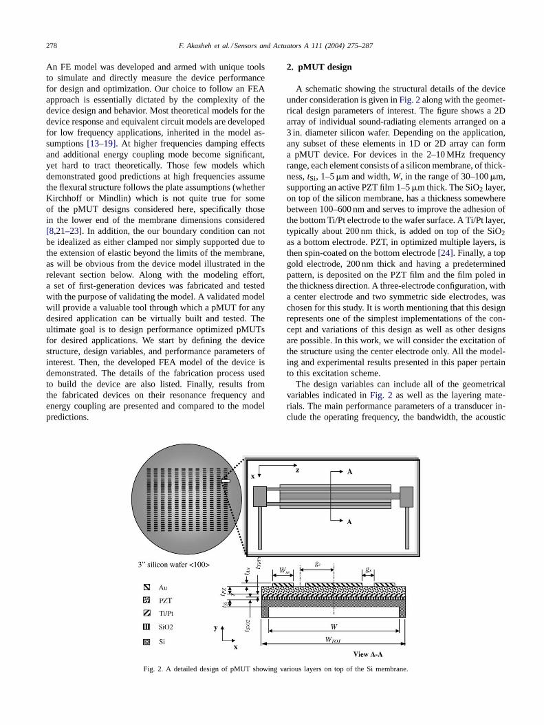
Fig. 2. A detailed design of pMUT showing various layers on top of the Si membrane.
2. pMUT design
A schematic showing the structural details of the deviceunder consideration is given inFig. 2along with the geomet-rical design parameters of interest. The figure shows a 2Darray of individual sound-radiating elements arranged on a3 in. diameter silicon wafer. Depending on the application,any subset of these elements in 1D or 2D array can forma pMUT device. For devices in the 2–10 MHz frequencyrange, each element consists of a silicon membrane, of thick-ness,tSi, 1–5�m and width,W, in the range of 30–100�m,supporting an active PZT film 1–5�m thick. The SiO2 layer,on top of the silicon membrane, has a thickness somewherebetween 100–600 nm and serves to improve the adhesion ofthe bottom Ti/Pt electrode to the wafer surface. A Ti/Pt layer,typically about 200 nm thick, is added on top of the SiO2as a bottom electrode. PZT, in optimized multiple layers, isthen spin-coated on the bottom electrode[24]. Finally, a topgold electrode, 200 nm thick and having a predeterminedpattern, is deposited on the PZT film and the film poled inthe thickness direction. A three-electrode configuration, witha center electrode and two symmetric side electrodes, waschosen for this study. It is worth mentioning that this designrepresents one of the simplest implementations of the con-cept and variations of this design as well as other designsare possible. In this work, we will consider the excitation ofthe structure using the center electrode only. All the model-ing and experimental results presented in this paper pertainto this excitation scheme.
The design variables can include all of the geometricalvariables indicated inFig. 2 as well as the layering mate-rials. The main performance parameters of a transducer in-clude the operating frequency, the bandwidth, the acoustic

F. Akasheh et al. / Sensors and Actuators A 111 (2004) 275–287 279
impedance, and the device effective coupling coefficient.The bandwidth refers to the width of the frequency rangeover which the transducer exhibits a significant responseand is a basic figure of merit for an ultrasonic transducer. Awider bandwidth is desirable as it implies a shorter impulseresponse time and a better system resolution[25]. The de-vice acoustic impedance and its relation to the characteristicacoustic impedance of the load medium is essential in deter-mining the energy transfer from the transducer to the load.For higher efficiency and improved bandwidth, the deviceacoustic impedance should closely match that of the loadmedium. The device coupling coefficientk2
eff measures theportion of the total electrical input energy that gets stored asmechanical energy in the form of elastic energy in the de-formed structure[26]. In our case, the mechanical energy ofconcern is that part of the total elastic energy which is storedin the first flexural mode, as it is the main mode throughwhich the device radiates sound. This stored energy repre-sents a ceiling on the energy that can be available for trans-duction. It is important to have a high coupling coefficientfor an ultrasonic transducer to be broadband and efficient[5].
In this work, we consider the design of a pMUT for thefrequency range of 2–10 MHz for operation in water as anexample. Such a system would have an axial resolution inthe range of 375–150�m, given an appropriate bandwidth.One application of such transducers is medical ultrasonicimaging of the human soft tissue, in particular, for the imag-ing of embryo and organs on the size scale of the heart of anadult. Soft human tissue, which represents a water-like load,has acoustic impedance very close to 1.5 MRayls, the acous-tic impedance of water. As such, the transducer needs to bedesigned with an acoustic impedance close to 1.5 MRayls,for efficient energy transfer. Due to the fact that the deviceeffective coupling coefficient,k2
eff , is central for a broadbandefficient transducer, the design process will aim at maxi-mizing k2
eff , while satisfying the requirements on the deviceresonance frequency and acoustic impedance. Another rea-son for maximizingk2
eff is that pMUTs, by their structure,have a small amount of the piezoactive material, which em-phasizes the need for a good coupling coefficient in orderto increase the maximum power that can be transmitted theacoustic port of the device.
3. Device model
Due to the complexity of the device behavior and to re-duce the experimental effort required to reach an optimizeddesign, an FE model integrating the electrical, mechanicaland acoustic fields, was developed to simulate the devicebehavior through modeling a single element representativeof an array, as shown in the lower right corner ofFig. 2.PZFlex, a commercial FEA package (Weidlinger AssociatesInc., Los Altos, CA), was used to build the model; however,special tools had to be developed and incorporated into the
package to allow for extracting device performance param-eters which can not be provided through the standard FEAoutput. In particular, two original tools for the measurementof the device coupling coefficient and acoustic impedancewere developed. The measurement of the coupling coeffi-cient k2
eff involves the extraction of the energy coupling tothe first standing flexural mode within the transducer (ne-glecting the non-radiating modes and the radiation from thehigher order modes, this is the mode that couples to thesound field and is therefore the one of interest). We choseto accomplish the measurement by comparing the energystored in the structure due to a step voltage excitation intwo cases: one where the radiating vibrational mode can befreely excited and the other where it is clamped. In bothcases, the electrical input energy is not allowed to leavethe system and, therefore, gets trapped either as mechanicalstrain energy in the deformed membrane or as stored elec-trical energy in the device capacitance. In the clamped case,no radiatable mechanical energy is stored and the detectedcharge on the electrodes measures the stored electrical andnon-radiatable mechanical energy,WE. In the free case, thedetected electrode charge measure the total stored energy,WT. The coupling coefficient can then be calculated from(WT − WE)/WT [26].
The acoustic impedance of the device is estimated bymatching the acoustic impedance of the load medium tothat of the device. (We are neglecting effects of compleximpedances.) In a manner analogous to the load impedancematching in an electrical circuit modeled by a voltage sourceof internal resistanceRS connected to a load of resistanceRL, maximum power transfer occurs when the load resis-tance is made equal to the source resistance. Under theseconditions, the peak velocity due to a pulse excitation{herechosen to be a Haversine of 2 V amplitude,V(t) = sin(2π×5e6t −π/2)+ 1} in the normal direction (Y-direction in ourcase) of any point on the membrane is equal to half the cor-responding value at no load (short circuit) condition and theacoustic impedance of the device matches that of the load;i.e.,ZD = ZL. The resonance frequency of the device is di-rectly determined by analyzing its time response under freevibration after a pulse excitation (again the same Haversineabove was used) has been applied, while the bandwidth isestimated from the frequency response of the normal veloc-ity of a central point on the membrane in the water loadedconditions. TheY-velocity history is transformed into thefrequency domain by applying the fast Fourier transform(FTT). From the resulting spectrum of the frequency re-sponse, the center frequency and the lower and upper “70%points” corresponding to a 3 dB (half power) reduction areextracted and used to calculate the bandwidth.
The fact that the membranes have the out-of-plane(Z-direction) dimension much larger than any of the mem-brane lateral dimensions (10:1 ratio at least), implies thata simplified 2D treatment can be used. To integrate theacoustic field into the model, a water layer, representing theacoustic load on the device, was added with an absorbing

280 F. Akasheh et al. / Sensors and Actuators A 111 (2004) 275–287
boundary condition at the device end that would not allowany reflections back[27].
4. Fabrication of pMUTs
In this section, a description of our device fabrication pro-cess is given. Basically, pMUT fabrication involves buildinga silicon membrane with electroded PZT layers on top. Tofabricate silicon membranes, anisotropic wet etching wasutilized with a boron etch stop. This approach allowed forcontrol of the membrane thickness by accurate control ofboron diffusion into one side of the wafer. The 3 in. siliconwafers (p-type〈1 0 0〉, 395–405�m) were wet oxidized at1050◦C to grow a 500 nm thick oxide. The oxide layer wasremoved from one side of the wafer using a buffered oxideetch (BOE). A boron soak was carried out to diffuse highconcentrations of boron into the exposed silicon using planarboron disks at a temperature of 1125◦C for 1 h. Borosilicateglass that forms on the surface of the boron-doped waferswas then removed using BOE. A subsequent sacrificial lowtemperature thermal oxide was grown at 850◦C. This ox-ide layer was removed using BOE, and then a final thermaloxide was grown at 850◦C for 3 h. The first sacrificial ox-ide was grown and removed to lower the residual stress in-duced by the high boron concentration near the surface ofthe wafer[28].
Standard photolithography techniques were used to createan oxide mask on the backside of the wafer. The wafers werethen etched with the anisotropic silicon etchant ethylene-diamine pyrocatechol (EDP) at 110◦C for 5.5 h to formSi/SiO2 membranes.Fig. 3 is a flow chart for the membraneprocessing. The thickness of the membrane was measuredto be 2.0�m using SEM (JSM-6400, JEOL, MA) with a100 nm oxide on the surface (Nanospec 210, Nanometrics,CA). The bottom electrodes consisting of 10 nm of titaniumand 200 nm of platinum, which were deposited using anelectron beam evaporation to the topside of the wafer.
PZT thin films are then deposited via spin coating of thePZT sol. The details of sol–gel processing of PZT can befound elsewhere[24]. A precursor solution was preparedconsisting of 2-methoxyethanol (2-MOE) as the solvent andstoichiometric amounts of anhydrous lead acetate, titaniumiso-propoxide, and zirconiumn-propoxide. Sequential sto-ichiometric additions of the starting chemicals, each fol-lowed by refluxing provided a 0.5 M precursor solution witha (52/48) morphotropic phase boundary (MPB) composi-tion. Spin coating was used for film deposition followed bya two temperature drying cycle at 150 and 350◦C. A total of15 layers were deposited, using a pre-sinter for every fourlayers at 700◦C for 10 min. This resulted in a 1�m thickfilm (Alpha Step 200, Tencor, CA). Top electrodes weredeposited by sputtering 10 nm of TiW and 200 nm of Au.These films were then patterned using standard photolithog-raphy techniques to create a top electrode with leads off themembrane. The PZT film was also patterned to expose the
Fig. 3. Schematic flow chart of silicon membrane fabrication.
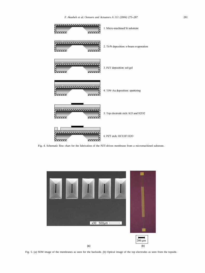
bottom electrode using a HCl:HF:H2O etchant.Fig. 4 illus-trates the processing sequence. Finally, the PZT film waspoled by applying a dc voltage of 15 V, which correspondsto 15 MV/m. Fig. 5 shows images of the membrane fromthe backside and the top electrodes from the topside.
5. Results
As mentioned earlier, the main goal at this point is to vali-date our model as a tool for designing optimized devices. Tothis end, we chose to pick one design variable, membranewidth W, and model its effect on the device performance,indicated by its resonance frequency and coupling coeffi-cient, while keeping the rest of the design variables fixed.Devices with corresponding designs and variable membranewidth were fabricated and tested for their actual resonancefrequency and coupling coefficient, and results compared.Membrane width is an important design parameter as itstrongly affects the membrane stiffness and, hence, the de-vice resonance frequency, acoustic impedance, bandwidth,and coupling coefficient. In all cases, the rest of the deviceparameters were fixed as follows: PZT film thickness,tPZT,1.0�m (a total of 15 layers), silicon membrane thickness,tSi, 2.0�m, bottom electrode thickness,tTi/Pt, 0.021�m,top electrode,tAu, 0.205�m, and silicon oxide layer,tSiO2,0.2�m. The top electrode configuration was fixed as follows:
F. Akasheh et al. / Sensors and Actuators A 111 (2004) 275–287 281
Fig. 4. Schematic flow chart for the fabrication of the PZT-driven membrane from a micromachined substrate.
Fig. 5. (a) SEM image of the membranes as seen for the backside. (b) Optical image of the top electrodes as seen from the topside.
282 F. Akasheh et al. / Sensors and Actuators A 111 (2004) 275–287
gap center location,gc, 14�m, gap size,gs, 10�m, and sideelectrode width,Wse, 8µm. In all cases, the center electrodeonly was excited with a Haversine signal:V(t) = sin(2π ×5e6t −π/2)+ 1. The choice of these values was dictated byour current fabrication capabilities and does not necessarilyrepresent an optimized device based on the modeling results.In fact, as will be shown later, the device with best predictedcoupling coefficient had different design parameters. Never-theless, the results are still important, as they help us validateour model and hence use it to predict pMUTs with optimizedproperties.
5.1. Modeling results
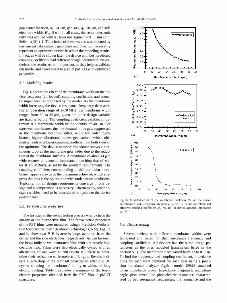
Fig. 6shows the effect of the membrane width on the de-vice frequency (air loaded), coupling coefficient, and acous-tic impedance, as predicted by the model. As the membranewidth increases, the device resonance frequency decreases.For an operation range of 2–10 MHz, the membrane widthranges from 80 to 35�m, given the other design variableare fixed as before. The coupling coefficient exhibits an op-timum at a membrane width in the vicinity of 40�m. Fornarrower membranes, the first flexural mode gets suppressedas the membrane becomes stiffer, while for wider mem-branes, higher vibrational modes get excited, which ulti-mately leads to a lower coupling coefficient on both sides ofthe optimum. The device acoustic impedance shows a con-tinuous drop as the membrane gets wider due to the reduc-tion of the membrane stiffness. A membrane of about 41�mwide ensures an acoustic impedance matching that of wa-ter at 1.5 MRayls, as set by the problem requirements. Thecoupling coefficient corresponding to this particular mem-brane happens also to be the maximum achieved, which sug-gests that this is the optimum device under those conditions.Typically, not all design requirements converge in one de-sign and a compromise is necessary. Alternatively, other de-sign variables need to be considered to optimize the deviceperformance.
5.2. Ferroelectric properties
The first step in the device testing process was to check thequality of the piezoactive film. The ferroelectric propertiesof the PZT films were measured using a Precision Worksta-tion ferroelectric tester (Radiant Technologies, NM).Fig. 7aand b, show twoP–E hysteresis loops acquired from thecenter and the side electrodes, respectively. As can be seen,the loops indicate well-saturated films with a relatively highcoercive field. Films were also electrically cycled with analternating square wave at 280 kV/cm at 10 kHz to deter-mine their resistance to ferroelectric fatigue. Results indi-cate a 37% drop in the remnant polarization after 3× 10⁸
cycles, showing the membranes’ ability to withstand longelectric cycling.Table 1provides a summary of the ferro-electric properties obtained from the PZT film in pMUTstructures.
Fig. 6. Modeled effect of the membrane thickness, W, on the deviceperformance. (a) Resonance frequency,f0 vs. W in air operation; (b)effective coupling coefficientk2
eff vs. W; (c) device acoustic impedancevs. W.
5.3. Device testing
Several devices with different membrane widths werefabricated and tested for their resonance frequency andcoupling coefficient. All devices had the same design pa-rameters as the ones modeled (parameters listed in theSection 5.1). The membrane sizes varied from 32 to 81�m.To find the frequency and coupling coefficient, impedanceplots for each were captured for each case using a preci-sion impedance analyzer, Agilent model 4294A, attachedto an impedance probe. Impedance magnitude and phaseangle plots reveal the piezoelectric resonance character-ized by two resonance frequencies: the resonance and the

F. Akasheh et al. / Sensors and Actuators A 111 (2004) 275–287 283
Fig. 7. Hysteresis loop obtained from an electrode pattern indicating excellent ferroelectric properties: (a) from a center electrode and (b) from thetwo-side electrodes.
Table 1Polarization and electric field measurements for 1�m PZT 52/48 thinfilm in pMUT structures
Average σ Range
Saturation polarization (�C/cm2) 56 2.3 51–59Remnant polarization (�C/cm2) 28 2.1 26–35Coercive field (kV/cm) 80 5.2 67–90
anti-resonance frequencies, which can be used to determinethe coupling coefficient using the relation[26]
k2eff
1 − k2eff
= F2a − F2
r
F2r
,
where Fr and Fa are the resonance and anti-resonancefrequency, respectively.Figs. 8 and 9show examples ofimpedance plots for two of the fabricated devices havingmembrane lateral dimensions (in-plane× out-of-plane) of44�m × 553�m and 71�m × 1066�m and tested in air.As can be seen in both plots, the typical characteristics of apiezoelectric resonance, where the impedance changes char-acter from capacitive to inductive at the resonance frequencyand back to capacitive at the anti-resonance frequency, isobvious. The corresponding change in the phase angle doesnot go up to+90◦, as expected for inductance, due tothe weak coupling of a pMUT, as predicted by the modeland measured experimentally. The estimated resonance fre-quency and coupling coefficient for the 44�m membrane
Fig. 8. Impedance magnitude and phase (Z–θ) plot shows the resonance of a 71�m wide membrane at 3.3 MHz in the case of air loading.
were 6.1 MHz and 0.035, while for the 71�m membranesthe corresponding values were 3.3 MHz and 0.024, respec-tively. The multiple resonances seen inFig. 9 indicate thatother vibration modes are being excited besides the mainmode of interest (the first flexural mode). The excitationof modes other than the one of interest is undesirable as itimpairs the energy coupling to the sound-radiating mode.
Fig. 10summarizes the results for the measured resonancefrequency and coupling coefficient of the tested membranesalong with the corresponding model prediction copied fromFig. 6for the convenience of making comparisons. Two setsof experimental data are shown by the scattered data points.Set 1 represents data for membranes having an out-of-planewidth of 533�m, while in Set 2 the membranes had anout-of-plane width of 1066�m. Both sets provide a validbasis for comparison to the model because a ratio of atleast 1:10 for the in-plane,W, to out-of-plane membranewidth is secured, thus allowing the membranes to practicallymeet the plane strain condition assumed in the FEA model.As can be seen, the modeled and the measured resonancefrequency results are in good agreement. This is not the casefor the coupling coefficient. A greater discrepancy betweenthe model prediction and the actual results exists.
6. Discussion
The good agreement between the predicted and mea-sured frequencies indicates that the model does capture the

284 F. Akasheh et al. / Sensors and Actuators A 111 (2004) 275–287
Fig. 9. Impedance magnitude and phase (Z–θ) plot shows multiple res-onances of a 44�m wide membrane. The primary resonance occurs at6.1 MHz (air-loaded case).
behavior of the device and can be used reliably to predictthe resonance frequency. The relatively large discrepancybetween the modeled and the measured coupling coefficientcan be analyzed in two aspects. First the wide dispersionof the measured data indicates that the electromechanicalproperties of the film are not consistent. Defects and incon-sistencies in the piezoelectric film can easily influence thepiezoelectric properties, hence the coupling, to a more ex-tent than they affect the mechanical properties of the mem-brane. Film defects include pinholes, microcracks due tolayered deposition interrupted with sintering heat treatment,and lattice misorientation. As the PZT is deposited via spincoating of precursor sol, inconsistencies in the solution anddeposited thickness are quite possible. The second aspectof disagreement between the modeled and measured valuesof the coupling coefficient is the general over-prediction bythe model. Several factor contribute to a lower actual cou-pling. The actual device has a significant parasitic capaci-tance that is not accounted for by the model. The parasiticcapacitance is mainly due to the additional capacitance in-troduced by the electroded PZT under the connection padsand leads running from the pads to the actual electrodeson top of the membrane, as illustrated byFig. 5. This por-tion of the PZT is not acting to drive the membrane, butis only acting to increase the portion of the total dielectricstored energy; thus, impairing the energy coupling of thedevice. An approximate idea about the effect of the para-sitic capacitance in reducing the coupling can be made bynoting that each of the connection pads has dimensions of100�m × 100�m while each of the three leads has dimen-sions of 375�m × 6�m. As such, the parasitic capacitanceamounts to about 72% of the capacitance of the PZT driv-ing the membrane. From a rough theoretical considerationstemming from the basic definition of the coupling coeffi-cient [26], this amount of parasitic capacitance will causethe coupling coefficient to drop to about 60% of the corre-sponding value in case it (the parasitic capacitance) did notexist. Table 2summarizes this point. As can be seen fromthe table, if the modeled coupling is adjusted to take the ef-fect of parasitic capacitance into account, the measured andpredicted values will be in fairly good agreement, especially
Fig. 10. (a) The measured resonant frequency in air operation, and (b)coupling coefficient as a function of membrane width excited by the centerelectrode only along with the corresponding model prediction shown bythe trendline.
if the dispersion in the measured coupling coefficient due tothe inconsistent quality of the film is resolved.
Another factor that can contribute to a lower than pre-dicted coupling coefficient is related to fabrication inaccu-racies. One such potential source of error in our fabricationprocess is the alignment of the membrane etched from thebackside of the wafer and the top electrode patterned fromthe front side of the wafer. Misalignment between the topelectrode and the membrane can excite undesirable vibra-tional modes, which will adversely influence the couplingcoefficient. Although this factor can have little effect in ourcase where only the center electrode is excited, it is expectedto have a significant effect in the case when all three elec-trodes are excited. Other fabrication errors, such as varia-tions in the various layers’ thickness can also lead to theexcitation of undesirable modes.
As the results indicate, the coupling coefficient of pMUTsis generally weaker that that of a bulk piece of PZT operatedas an extensional or thickness mode resonator. A PZT-5Hstrip, such as those commonly used for ultrasonic transduc-ers, properly electroded and poled to operate as extensionalresonator, will have a coupling coefficient (k2
33 in this case)of 0.5 compared to a maximum of 0.037 seen in this study

F. Akasheh et al. / Sensors and Actuators A 111 (2004) 275–287 285
Table 2Summary of the effect of parasitic capacitance on the disagreement between the measured and predicted values of the coupling coefficient
Membranewidth, W (�m)
(a) Modeled couplingcoefficient,k2
eff(parasitic capacitancenot accounted for)
(b) Modeled couplingcoefficient,k2
eff(parasitic capacitanceaccounted for)
Ratio of k2eff in
column (a) tok2eff
in (b) (%)
(c) Measuredk2eff Error in k2
eff ,|[(a) − (c)]/(c)|(%)
Error in k2eff ,
|[(b) − (c)]/(c)|(%)
32 0.035 0.021 59.0 0.027 29.6 22.241 0.037 0.022 59.1 0.023 60.9 4.344 0.037 0.022 59.1 0.035 5.7 37.150 0.034 0.020 59.0 0.026 30.8 23.153 0.032 0.019 58.9 0.020 60.0 5.063 0.031 0.019 58.9 0.021 47.6 9.571 0.034 0.020 59.0 0.024 41.7 16.776 0.031 0.018 58.9 0.016 93.4 12.5
where that membrane width was the only design variable tobe varied. Obviously, to explore the possibility of achiev-ing higher coupling with our device, a more comprehensiveoptimization including the other design variables must beundertaken. In a previous study, we presented the detailsof a comprehensive theoretical optimization of the couplingcoefficient, which included all the design parameters[29].Through a study of the effect of each design variable on thedevice coupling, three parameters, the PZT film thickness,tPZT, the silicon membrane thickness,tSi, and the top elec-trode design (in itself having three parameters: gap centerlocation,gc, gap size,gs, and side electrode width,Wse) wereidentified as the ones mostly affecting the coupling. Opti-mizing these variables, the coupling coefficient was shownto improve up to 0.092 for the particular pMUT design con-sidered here (thek31 bending mode device). Furthermore,a preliminary investigation of a pMUT with a modified de-sign, referred to as thek33 bending mode device, showeda coupling coefficient of 0.17. In this design, an in-planepoling scheme, as opposed to the through-thickness polingof the PZT film in thek31 device, allows the strongerk33piezoelectric coupling effect to drive the membrane in bend-ing, thus providing a generally higher energy coupling tothe first bending mode, i.e., to sound-radiating mode[30].In any case, in spite of a low coupling coefficient, pMUTsstill has the advantage of wide bandwidth compared to con-ventional transducers. A modern ultrasonic transducer has abandwidth of 75–80%. The model prediction for the pMUTdevice modeled earlier and having a membrane width of41�m indicates a bandwidth of 103%, which represents asignificant performance advantage.
7. Conclusions
The development of pMUTs, including design, fabricationand testing, was investigated. An FEA model, with originaltools to measure the device performance, was developed tohelp design and optimize the devices. Devices were fabri-cated and their performance tested and compared to modelpredications, which were found to be in good agreement.
The validated model can be a very useful tool, saving greatdeal of experimental effort, for the design and optimizationpMUTs for different purposes. Our investigation proved thatpMUTs is a viable concept. The flexibility in tailoring theirfrequency and acoustic impedance increases the potentialof their application in various fields. Compared to conven-tional transducers, pMUTs offer the advantage of superiorperformance as far as bandwidth is concerned. In spite oftheir lower coupling coefficient, there is a potential of sig-nificantly improving it. In this work, our main focus wason thek31 device due to its simplicity, however, a brief in-vestigation of a modified design, thek33 device, proved animprovement of about 100% in the device coupling. Otheradvantage lie in the fact that pMUTs are more compact andtheir fabrication is more convenient, allowing for new ap-plications such as 3D and high frequency imaging. Finally,pMUTs are expected to have a cost advantage due to theirmass fabrication by the matured IC fabrication techniques.
Acknowledgements
The authors wish to express their gratitude to the financialsupport of Washington Technology Center (WTC), WA, andPhilips Ultrasound, Bothell, WA. We also acknowledge thecontribution of Oliver Huang and Gabe Kuhn to the exper-imental effort in device fabrication. Thanks are also due tothe engineering team at Weidlinger Associates Inc., CA, inparticular to Dr. Paul Reynolds, for their persistent techni-cal support with their PZFlex software package, used in thiswork. Last but not least, the first author would like to thankDr. Michael Anderson, at University of Idaho, for many in-sightful discussions.
References
[1] W.P. Robbins, Ferroelectric-based microactuators, Integr. Ferroelect.11 (1995) 179.
[2] A. Goldstein, R.L. Powis, Medical ultrasonic diagnostics, in: R.NThurston, A.D. Pierce (Eds.), Ultrasonic Instruments and DevicesI, in: E. Papadakis (volume ed.), Physical Acoustics, vol. XXIII,Academic Press, New York, 1999, pp. 43–191.

286 F. Akasheh et al. / Sensors and Actuators A 111 (2004) 275–287
[3] I. Ladabaum, X. Jin, H.T. Soh, A. Atalar, B.T. Khuri-Yakub, Sur-face micromachined capacitive ultrasonic transducers, IEEE Trans.Ultrason. Ferroelectr. Freq. Contr. 45 (3) (1998) 678.
[4] R.L. Goldberg, S.S. Smith, J. Mottley, K.W. Ferrara, Ultrasound,in: J.D. Bronzino (Editor-in-Chief), The Biomedical EngineeringHandbook, vol. 1, second ed., CRC Press LLC, Boca Raton, 2000,pp. 65-1–65-23.
[5] N.F. Foster, Piezolectric and piezoresistive properties of films, in:L.I. Maissel, R. Glang (Eds.), Handbook of Thin Film Technology,McGraw-Hill, New York, 1970 (Chapter 15).
[6] P. Osbond, C.M. Beck, C.J. Brierley, M.R. Cox, S.P. Marsh, N.M.Shorrocks, The influence of ZnO and electrode thickness on the per-formance of thin film bulk acoustic wave resonators, in: Proceedingsof the IEEE Ultrasonics Symposium, 1999, pp. 911–914.
[7] P.C. Eccardt, K. Neiderer, Micromachined ultrasonic transducers withimproved coupling factors from a CMOS compatible process, Ultra-sonics 38 (2000) 744.
[8] J.J. Bernstein, S.L. Finberg, K. Houston, L.C. Niles, H.D. Chen,L.E. Cross, K.K Li, K. Udayakumar, Micromachined high frequencyferroelectric sonar transducers, IEEE Trans. Ultrason. Ferroelectr.Freq. Contr. 44 (5) (1997) 960–969.
[9] G. Percin, B.T. Khuri-Yakub, Micromachined 2-D array piezoelectri-cally actuated flextensional transducers, in: Proceedings of the IEEEUltrasonic Symposium, vol. 2, 1997, pp. 959–962.
[10] T. Khuri-Yakub, et al., Silicon micromachined ultrasonic transducers,Jpn. J. App. Phys. 39 (2000) 2883–2887.
[11] O. Oralkan, Simulation and experimental characterization of a 2-D,3-MHz capacitive micromachined ultrasonic transducer (CMUT) ar-ray element, in: Proceedings of the IEEE Ultrasonics Symposium,1999, pp.1141–1144.
[12] P. Reynolds, J.D. Fraser, Finite element determination of effectiveelectromechanical coupling coefficient with applications to piezo-electric and electrostatic transducers, Ultrasonics International 2001,Technical University of Delft, Delft, The Netherlands, 2–5 July 2001.
[13] C.P. Germano, Flexure mode piezoelectric transducers, IEEE Trans.Audio Electroacoust. AU-19 (1973) 6–12.
[14] W.J. Denkmann, R.E. Nickell, D.C. Strickler, Analysis ofstructural–acoustic interactions in metal–ceramic transducers, IEEETrans. Audio Electroacoust. AU-21 (4) (1973) 317–324.
[15] Y.T. Antonyak, M.E. Vassergiser, Calculation of the characteristics ofa membrane-type flexural-mode piezoelectric tranducer, Sov. Phys.Acoust. 28 (3) (1982) 176–180.
[16] E.S. Brailov, M.E. Vassergiser, Estimation of the characteristics of adisk-shaped flexural-mode bimorph cell, Sov. Phys. Acoust. 26 (4)(1980) 325–328.
[17] M.E. Vassergiser, A.N. Vinnichenko, A.G. Dorosh, Calculation andinvestigation of flexural-mode piezoelectric disk transducers on apassive substrate in reception and radiation, Sov. Phys. Acoust. 38 (6)(1992) 558–561.
[18] N.T. Adelman, Y. Stavsky, Flexural-extensional behavior of compos-ite piezoelectric circular plates, J. Acoust. Soc. Am. 67 (3) (1980)819–822.
[19] B.S. Aronov, L.B. Nikitin, Calculation of the flexural modes ofpiezoceramic, Acoustics 27 (5) (1981) 382–387.
[20] P. Muralt, D. Schmitt, N. Ledermann, J. Baborowski, P.K. Weber, W.Steichen, S. Petitgrang, A. Bosseboeuf, N. Setter, P. Gaucher, Studyof PZT coated membrane structures for micromachined ultrasonictransducers, 2001 IEEE Ultrasonics Symposium, pp. 907–911.
[21] S.H. Chang, Y.C. Tung, Electro-elastic characteristics of asymmetricrectangular piezoelectric laminae, IEEE Trans. Ultrason. Ferroelectr.Freq. Contr. 46 (4) (1999) 950–960.
[22] G. Percin, B.T. Khuri-Yakub, Piezoelectrically actuated flextensionalmicromachined ultrasonic transducers. I. Theory, IEEE Trans. Ultra-son., Ferroelect., Freq. Contr. 49 (5) (2002) 573–584.
[23] G. Percin, B.T. Khuri-Yakub, Piezoelectrically actuated flextensionalmicromachined ultrasonic transducers. II Fabrication and experi-
ments, IEEE Trans. Ultrason. Ferroelect. Freq. Contr. 49 (5) (2002)585–595.
[24] T. Myers, P. Banerjee, S. Bose, A. Bandyopadhyay, Layered lead zir-conate titanate and lanthanum-doped lead zirconate titanate ceramicthin films, J. Mater. Res. 17 (9) (2002) 2379–2385.
[25] F. Akasheh, J.D. Fraser, S. Bose, A. Bandyopadhyay, Piezoelectricmicromachined ultrasonic transducers (pMUTs): influence of struc-tural parameters on device performance, IEEE Trans. Ultrason. Fer-roelect. Freq. Contr., submitted for publication.
[26] ANSI/IEEE Std 176-1987, IEEE Standard on Piezoelectricity, TheInstitute of Electrical and Electronics Engineers, New York, USA.
[27] N.N. Abboud, G.L. Wojcik, D.K. Vaughan, J. Mould, D.J. Powell,L. Nikodym, Finite element modeling for ultrasonic transducers,in: Proceedings of the SPIE International Symposium on MedicalImaging, San Diego, 21–27 February 1998.
[28] G. Kuhn, T. Myers, S. Bose, A. Bandyopadhyay, Mechanical prop-erties of boron doped Si and Si/SiO2 membranes, Mater. Res. Soc.Symp. Proc. 729 (2002).
[29] F. Akasheh, J.D. Fraser, S. Bose, A. Bandyopadhyay, Piezoelectricmicromachined ultrasonic transducers (pMUTs): influence of struc-tural parameters on device performance, in preparation.
[30] B. Xu, L.E. Cross, J.J. Brenstein, Ferroelectric and antiferroelectricfilms for microelectromechanical systems applications, Thin SolidFilms 377–378 (2000) 712–718.
Biographies
Firas Akasheh received his masters degree in mechanical engineering fromthe School of Mechanical and Materials Engineering at Washington StateUniversity in 2002. His MS research was on modeling of piezoelectricmicromachined ultrasonic transducers (pMUTs), where he worked withATL Ultrasound (currently, Philips) to develop a predictive model usingfinite element analysis for the optimization of critical design parametersto improve performance of pMUTs. Presently, he is pursuing his PhD incomputational mechanics at Washington State University. Before startinghis graduate studies, he worked in aluminum extrusion and aluminumextrusion die design and production industries for 7 years.
Todd B. Myers received his masters in materials science and engineer-ing in 2002 from the School of Mechanical and Materials Engineeringat Washington State University. His initial research as an undergraduatefocused on the synthesis and processing lead zirconate titanate (PZT)thin films and their derivatives. The focus progressed as graduate studentinto silicon micro-machining with PZT thin film integration in an effortto develop PZT driven micro electromechanical systems (MEMS). Heis currently employed by the Intel Corporation and focused on develop-ing electronic packaging technologies for communications, wireless, andmemory applications.
John D. Fraser received a BS in applied physics from Caltech in 1973,and a PhD in applied physics from Stanford University in 1979, special-ized in ultrasonic transducers. Form 1978 to 1990, he was a founder andvice-president of Precision Acoustic Devices, Inc., a small business sup-plying medical and nondestructive testing ultrasonic transducers. Duringthat time he was Principal Investigator on three SBIR grants. In 1990,PAD was purchased by ATL Ultrasound, and then ATL was purchased byPhilips Medical Systems. John is currently corporate scientist for Trans-ducer R&D at Philips. His current research activities center on highlyaccurate modeling of ultrasonic transducer behavior, and novel high per-formance ultrasonic transduction techniques. He has over 16 publishedpapers, and 15 patents.
Susmita Bose received her BS in chemistry from the University ofKalyani (India) in 1990, MS in Chemistry from the Indian Institute ofTechnology–Kanpur in 1992 and Ph.D. in physical–organic chemistry

F. Akasheh et al. / Sensors and Actuators A 111 (2004) 275–287 287
from Rutgers–the State University of New Jersey in 1998. She workedas a research assistant professor in the School of Mechanical and Mate-rials Engineering at Washington State University from 1998 to 2001 andbecame an assistant professor in 2001. Her research interests include syn-thesis and processing of nano-structured materials for piezoelectric, bioand structural applications. Prof. Bose received CAREER award in 2002from the National Science Foundation. She has published 35 technicalarticles.
Amit Bandyopadhyay received his BS in metallurgy from Jadavpur Uni-versity (India) in 1989, MS in metallurgy from the Indian Institute of
Science–Bangalore in 1992 and PhD in materials science and engineer-ing from the University of Texas at Arlington in 1995. He worked as aresearch associate at the Center for Ceramics Research at Rutgers Uni-versity from 1995 to 1997 and joined the School of Mechanical and Ma-terials Engineering at Washington State University in 1997 as an assistantprofessor, and became an associate professor in 2001. His research in-terest lies with processing and characterization of piezoelectric, bio andstructural materials. He has received the CAREER award from the Na-tional Science Foundation in 1999 and the Young Investigator ProgramAward from the Office of Naval Research in 1998. He holds 8 US patents,published 82 technical articles and edited 1 book.