Embed Size (px)
Citation preview

micromachines
Review
Advances in Capacitive MicromachinedUltrasonic Transducers
Kevin Brenner 1,† , Arif Sanli Ergun 1,2,† , Kamyar Firouzi 1,† , Morten Fischer Rasmussen 1,† ,Quintin Stedman 1,† and Butrus (Pierre) Khuri–Yakub 1,*,†
1 E.L. Ginzton Lab., Stanford University, Stanford, CA 94305, USA; [email protected] (K.B.);[email protected] (A.S.E.); [email protected] (K.F.); [email protected] (M.F.R.);[email protected] (Q.S.)
2 Department of Electrical and Electronics Engineering, TOBB University of Economics and Technology,Ankara 06560, Turkey
* Correspondence: [email protected]; Tel.: +1-650-723-0718† These authors contributed equally to this work.
Received: 15 January 2019; Accepted: 18 February 2019; Published: 23 February 2019�����������������
Abstract: Capacitive micromachined ultrasonic transducer (CMUT) technology has enjoyed rapiddevelopment in the last decade. Advancements both in fabrication and integration, coupled withimproved modelling, has enabled CMUTs to make their way into mainstream ultrasound imagingsystems and find commercial success. In this review paper, we touch upon recent advancements inCMUT technology at all levels of abstraction; modeling, fabrication, integration, and applications.Regarding applications, we discuss future trends for CMUTs and their impact within the broad field ofbiomedical imaging.
Keywords: capacitive micromachined ultrasonic transducer (CMUT); acoustics; micromachining;capacitive; transducer; modelling; fabrication
1. Introduction
The capacitive micromachined ultrasonic transducer (CMUT) started with an idea to make a betterairborne ultrasound transducer operating in the MHz frequency range [1]. Later, a simple underwaterexperiment showed the huge advantage in bandwidth over piezoelectric transducers and motivatedthe development of a sealed CMUT for immersion applications [2]. A CMUT consists of a flexible topplate suspended over a gap. Transduction is achieved electrostatically, in contrast with piezoelectrictransducers. The merit of the CMUT derives from having a very large electric field in the cavity of thecapacitor, a field of the order of 108 V/m or higher results in an electro-mechanical coupling coefficientthat competes with the best piezoelectric materials. The availability of micro-electro-mechanical-systems(MEMS) technologies makes it possible to realize thin vacuum gaps where such high electric fields canbe established with relatively low voltages. Thus, viable devices can be realized and even integrateddirectly on electronic circuits such as complimentary metal-oxide-semiconductor (CMOS). A further andvery important development was the discovery of collapse mode operation of the CMUT. In this mode ofoperation, the CMUT cells are designed so that part of the top plate is in physical contact with the substrate,yet electrically isolated with a dielectric, during normal operation. The transmit and receive sensitivities ofthe CMUT are further enhanced thus providing a superior solution for ultrasound transducers [3]. In short,the CMUT is a high electric field device, and if one can control the high electric field from issues like
Micromachines 2019, 10, 152; doi:10.3390/mi10020152 www.mdpi.com/journal/micromachines
Micromachines 2019, 10, 152 2 of 27
charging and breakdown, then one has an ultrasound transducer with superior bandwidth and sensitivity,amenable for integration with electronics, manufactured using traditional integrated circuits fabricationtechnologies with all its advantages, and can be made flexible for wrapping around a cylinder or evenover human tissue.
In this paper, we will review the various aspects of CMUT technology: theory of operation, fabricationwith surface and bulk micromachining, electronic integration methods, characterization, and applications.Beyond this overview, further details in the above-named topics will be left to the references.
2. Theory and Modeling of Capacitive Ultrasonic Transduction
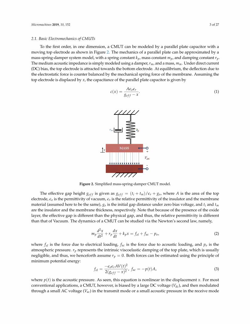
A CMUT element typically consists of several cells connected in parallel. Each cell is composed of aflexible top plate (also referred to as top electrode) anchored around its edges. A shallow gap is formedbetween this flexible top plate and a fixed bottom plate. These two plates are made electrically conductive(partially or completely) to form a capacitor with the gap in-between (Figure 1a), making the CMUT cell avariable capacitor. A CMUT presents a challenging modeling problem as multiple physics are involved inits operation. As with any other MEMS device, at the basic level, the mechanics of the plate needs to bemodeled along with the electrodynamics. Moreover, a CMUT interacts with an acoustic medium suchas air or water to radiate or sense ultrasound; so, the interaction of the acoustic medium with the CMUTplate also needs to be modeled.
(a) (b)Figure 1. Capacitive micromachined ultrasonic transducer (CMUT) cell illustration. (a) A CMUT cell iscomposed of a flexible top plate and a fixed bottom plate. (b) A direct current (DC) bias is applied duringthe operation that deflects the top plate.
Mechanical systems can be converted into electrical circuits by using the analogy between themechanical and the electrical domains. One way to implement this analogy is to replace the forces inthe mechanical domain by voltage sources and velocities by electrical currents. The models of this typeare called equivalent circuit models. This methodology serves as a powerful tool for the analysis ofelectromechanical systems. Equivalent circuit models have been widely used for design and optimizationof variety of transducer technologies such as piezoelectric [4] and an CMUTs [5,6].
Advancement in contemporary computing and equivalent circuits has enabled more detailedtwo-dimensional and three-dimensional finite element (FE) models to calculate the collapse voltage,output pressure, bandwidth, sensitivity, and crosstalk. Finite element models are designed to solve to theexact coupled-field theory of electrostatics, solid mechanics, and acoustics. A variety of finite element toolshave been deployed, including but not limited to, ANSYS, COMSOL, COVENTOR, LS-DYNA, PZFlex,as well as custom-made modeling tools [7].
In the following sub-sections, we first explain the basic electromechanics of CMUTs using a simpleparallel plate model. Next, we review the basics of equivalent circuit and finite element modeling.
Micromachines 2019, 10, 152 3 of 27
2.1. Basic Electromechanics of CMUTs
To the first order, in one dimension, a CMUT can be modeled by a parallel plate capacitor with amoving top electrode as shown in Figure 2. The mechanics of a parallel plate can be approximated by amass-spring-damper system model, with a spring constant kp, mass constant mp, and damping constant rp.The medium acoustic impedance is simply modeled using a damper, rm, and a mass, mm. Under direct current(DC) bias, the top electrode is attracted towards the bottom electrode. At equilibrium, the deflection due tothe electrostatic force is counter balanced by the mechanical spring force of the membrane. Assuming thetop electrode is displaced by x, the capacitance of the parallel plate capacitor is given by
c(x) =Aεoεr
ge f f − x. (1)
Figure 2. Simplified mass-spring-damper CMUT model.
The effective gap height ge f f is given as ge f f = (ti + tm)/εr + go, where A is the area of the topelectrode, εo is the permittivity of vacuum, εr is the relative permittivity of the insulator and the membranematerial (assumed here to be the same), go is the initial gap distance under zero bias voltage, and ti and tm
are the insulator and the membrane thickness, respectively. Note that because of the presence of the oxidelayer, the effective gap is different than the physical gap, and thus, the relative permittivity is differentthan that of Vacuum. The dynamics of a CMUT can be studied via the Newton’s second law, namely,
mpd2xdt2 + rp
dxdt
+ kpx = fel + fac − po, (2)
where fel is the force due to electrical loading, fac is the force due to acoustic loading, and po is theatmospheric pressure. rp represents the intrinsic viscoelastic damping of the top plate, which is usuallynegligible, and thus, we henceforth assume rp = 0. Both forces can be estimated using the principle ofminimum potential energy:
fel =−εoεr AV(t)2
2(ge f f − x)2 , fac = −p(t)A, (3)
where p(t) is the acoustic pressure. As seen, this equation is nonlinear in the displacement x. For mostconventional applications, a CMUT, however, is biased by a large DC voltage (Vdc), and then modulatedthrough a small AC voltage (Vac) in the transmit mode or a small acoustic pressure in the receive mode
Micromachines 2019, 10, 152 4 of 27
(leading to induction of a small Vac). This assumption serves as a basis for linearization of the electrostaticforce at Vdc and xdc. After expanding the total voltage and displacement as V = Vdc +Vac and x = xdc + xac,and dropping the second order terms, the linearized equation of motions becomes:
(mp + mm)d2xac
dt2 + rmdxac
dt+ (kp − ks)xac =
−εoεr AVdcVac(t)2(ge f f − xdc)2 , (4)
with
ks =εoεr AVdc
2
(ge f f − xdc)3 , (5)
where ks is known as the spring softening effect, which is a function of the DC bias, and implies theresonance frequency of the CMUT shifts as the DC bias increases. As the top electrode moves closerto the bottom electrode due to the applied voltage, the electrical field increases, and the top electrodedisplaces further, acting as if the spring constant of the top electrode decreases under the influence of theapplied voltage. Also, mm and rm are the effect of acoustic loading, which we shall discuss in-depth laterin this section.
The DC components can be calculated by solving kpxdc = fel − po. In absence of the atmosphericpressure, this leads to
Vdc =
√2kpxdc
εoεr A(ge f f − xdc), (6)
which implies an important phenomenon; if the bias voltage is increased beyond a certain value, the topelectrode collapses onto the bottom electrode. This means that the displacement of the top electrodecan result in an increase in the electric field to the point where the attractive electrostatic force cannotbe balanced by the spring force, resulting in the collapse of the top electrode onto the bottom electrode.Mathematically, this occurs when the gradient of the electrostatic force is larger than the gradient of themechanical force. One can calculate the collapse voltage by equating the gradient of the electrostatic forceto zero:
Vcoll =√
8kg3e f f /27εoεr A, (7)
and thus, it can be seen that displacement at Vcoll is ge f f /3.
2.2. Small-Signal (Linear) Equivalent Circuit Model
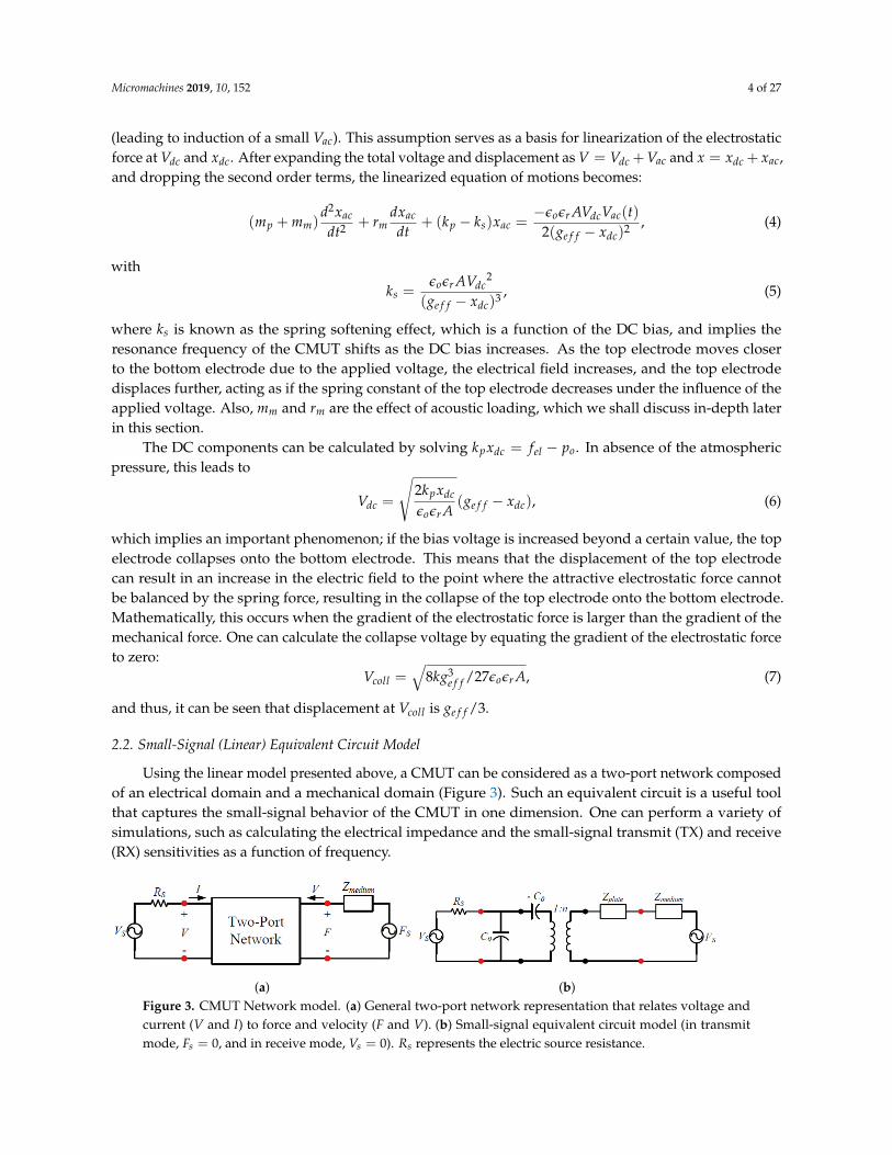
Using the linear model presented above, a CMUT can be considered as a two-port network composedof an electrical domain and a mechanical domain (Figure 3). Such an equivalent circuit is a useful toolthat captures the small-signal behavior of the CMUT in one dimension. One can perform a variety ofsimulations, such as calculating the electrical impedance and the small-signal transmit (TX) and receive(RX) sensitivities as a function of frequency.
(a) (b)Figure 3. CMUT Network model. (a) General two-port network representation that relates voltage andcurrent (V and I) to force and velocity (F and V). (b) Small-signal equivalent circuit model (in transmitmode, Fs = 0, and in receive mode, Vs = 0). Rs represents the electric source resistance.
Micromachines 2019, 10, 152 5 of 27
In the electrical part, Co is the clamped capacitance of the device at the bias voltage and −Co representsthe spring softening capacitance. Vs and Rs represent the input voltage source and its electric resistance.The mechanical membrane and medium acoustic impedances constitute the mechanical part. Fs is theforce due to an acoustic pressure source, i.e., Fs = pA. The two parts are coupled together through anelectromechanical transformer, picturing a CMUT as a device that transforms electrical energy to mechanicalenergy and vice versa. For a parallel plate capacitor, the electric field and transformer ratio are given by
Eo =Vdc
ge f f − xdc, Co =
εoεr Age f f − xdc
, n = EoCo. (8)
Note also that it is easy to verify n =√
ksCo. When the transducer is operated in vacuum,the mechanical port of the circuit is short-circuited. For immersion devices, the mechanical port issimply terminated by the radiation impedance. In transmit mode, Fs = 0, and in receive mode, Vs = 0.
The maximum small signal output pressure of the transducer can be easily calculated using theequivalent circuit method. The maximum output pressure is obtained at the resonant frequency of themembrane, where all the reactive elements cancel each other out in the mechanical part of the circuit.At this frequency, the output pressure per volt is simply
pmax =nA
=εoVdc
(ge f f − xdc)2 , (9)
and for a bias voltage close to the collapse voltage, is pmax =√
3kεo/2Age f f . In equivalent circuitmodeling, the mechanical impedance of the plate is determined by subjecting the plate to a harmonicloading, semi-analytically using either the classical plate theory [5] or finite element method [8,9], in caseswhere analytical solutions are either tedious or do not exist. This can be used to derive the impedance ofplates of various shapes such as circular, rectangular, or hexagonal geometries, or under different boundary(clamping) conditions.
The medium in which the transducer is operating presents an impedance (Zmedium) to the transducerthat must be included in the small-signal equivalent circuit model (see Figure 3b) and can be considered asZmedium = Za A, where Za is the characteristic acoustic impedance of the plate as a radiator of sound (notto be confused with mechanical impedance). However, since the transducer is in general a small resonator(compared to the wavelength) Za can be quite different than that of a plane wave. For a circular pistontransducer of radius a, within an infinite rigid baffle, this acoustic impedance is given by [10]
Za = Zo
(1− J1(2ka)
ka+ j
H1(2ka)ka
), (10)
where J1 is the Bessel function of the first kind and the first order and H1 is the Struve function of thefirst order. Zo is the plane wave impedance (Zo = ρoco), where ρo and co are the density and speed ofsound in the loading fluid. k = ω/co is the wave number. Note that Za has both real and imaginary parts.The real part contributes to the acoustic damping through rm and is known as the radiation impedance.rm is the mechanism by which a CMUT radiates sound. The imaginary part contributes to the mass termthrough mm, and thereby results in shift in the resonance frequency. In summary, rm = jωARe{Za} andmm = jωAIm{Za}.
Having a complete model, one can now determine the resonance frequency as well as transmit andreceive sensitivities. The resonance frequency and fractional bandwidth (FBW) are
Micromachines 2019, 10, 152 6 of 27
ωo =
√kp − ks
mp + mm, FBW =
rm√(mp + mm)(kp − ks)
. (11)
For transmit and receive sensitivities, STX and SRX , it can be shown that
STX =∣∣∣Pout
Vin
∣∣∣ = STX,maxΞ(ω), SRX =∣∣∣ Iout
Pin
∣∣∣ = SRX,maxΞ(ω), (12)
where STX,max = n/A, SRX,max = nA/rm and
Ξ(ω) =[1 +
( ω
rm(mp + mm)
)2(1− ωo
ω
)2]− 12. (13)
2.3. Finite Element Modeling
An equivalent circuit model using lumped parameters serves to provide a good approximation butsuch an approach has many limitations and may not represent all the underlying physics. Finite elementanalysis is ideal for analyzing such multi-physics systems. The underlying physics for the CMUT operationcan be described using partial differential equations with some boundary conditions. Depending on theshape, geometry, and mode of operation of CMUTs, a diverse array of finite element procedures havebeen developed over the years. In the finite element method, the simulation domain is divided into manysmall elements, called finite elements, over which a much simpler function is used to approximate the truesolution. A set of linear equations is formulated based on minimizing the error between this approximatesolution and the true solution.
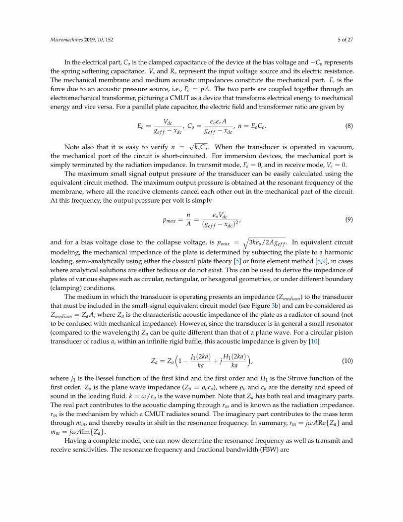
Conventional CMUTs have been simulated using finite element analysis as described by [11,12].Depending on the geometry and structure of the CMUT, Finite element models have been implementedin two-dimensions (2D), two-dimensions with axial symmetry (2D-Axisym.), and three-dimensions (3D)models. In the simplest form, the equations of linear elasticity (both static and dynamic) have been used tocapture the mechanics of the vibrating plate. Finite element methods have made it possible to includevarious mechanical nonlinearities with ease. Perhaps the most prevalent one is geometric nonlinearity(also referred to as stress stiffening) in thin CMUT plates (where the thickness to diameter ratio is less than5%). Stress stiffening is a nonlinear signature, where the vibrating plate stiffens as it is being deformeddue to the second order effects of the strain.
The plate is usually anchored at the edges and is immersed in an acoustic medium (i.e., a domain thatis governed by the acoustic wave equation). Often, the acoustic domain is terminated at the outer edges(at a certain distance from the plate) via some form of absorbing boundary conditions (ABC) or a perfectlymatched layer (PML). This is usually used in the transmit mode and intended to absorb all out-goingwaves, and thus, model a CMUT cell pulsating in an infinite half-space. To investigate the operation ofa single CMUT cell, generally a spherical absorbing boundary is used to emulate the acoustic radiationcondition (Figure 4a). For investigating an array of CMUT cells, it is practically not possible to model allthe cells, unless the array has a small number of cells or has a specific type of symmetry. The standardprocedure to model an array of CMUT cells is known as the wave-guide model, where a single cell CMUTis modeled, however, with periodic boundary conditions (both in 2D and 3D). The wave-guide modelis more subtle in axially symmetric geometries, where symmetry boundary conditions (as opposed toperiodic conditions) have been widely adopted to mimic the effect the neighboring cells with a goodaccuracy [12–14] (see Figure 4b). The wave-guide models are also used in the receive mode, in the regimeswhere the incident wavelength is much larger than the dimensions of the CMUT cell.
Micromachines 2019, 10, 152 7 of 27
(a) (b)Figure 4. Geometry and boundary conditions of 2D-Axisym. CMUT finite element (FE) models. (a) Singlecell model. (b) Wave-guide model.
Care should be taken, however, when using the wave-guide model. The model shown in Figure 4bgenerates sound waves in the fluid when the membrane is excited. The field quickly converges into planewaves as it propagates away from the membrane and the wave-fronts become parallel to the membraneplane and absorbing boundary. Below a certain cut-off frequency the fluid wave-guide only supportsplane-waves, which is ideal for the purpose of modeling the CMUT cell. However if the frequencyis high enough, there are also waves propagating at an oblique angle. The cut-off frequency of thewave-guide is given by fc = 1.22vL/2rout, where vL is the sound velocity in the fluid and rout is theradius of the wave-guide. Above this frequency, due to the oblique incidence on the absorbing boundary,some part of the incidence wave gets reflected at the absorbing boundary. This results in standing wavesin the wave-guide.
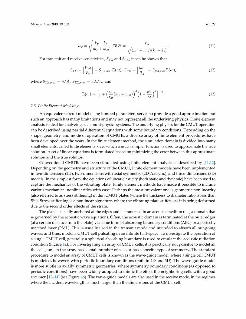
Perhaps the most challenging FE modeling of CMUTs is the electrostatic force (or variable capacitance),which is inversely proportional to the deformed gap. As such, different Element technologies have beenapplied, depending on the Software being used. We elaborate on two here: (1) ANSYS: the electrical portsare added to the membrane by segmenting the gap into many parallel plate capacitors as shown in Figure 5.This approach neglects the fringing fields and assumes that the electric field is always perpendicular to theelectrodes. (2) COMSOL: the gap is meshed and modeled by solving the actual equation of electrostaticswith a deformed mesh. The last part is necessary as the gap changes in response to the pressure or electricalfields. The coupling between the electric field and vibrating plate is through the electromechanical forcethat is calculated at the top electrode by the Maxwell’s stress tensor [15].
Figure 5. CMUT electrostatic gap segmentation. The electrostatic force is approximated by adding severalparallel plate capacitors between the top and bottom electrodes.
Using the above model one can perform static, harmonic (small signal frequency domain),and transient (large signal time domain) analyses. For small signal analyses, static calculation is first usedto pre-stress the plate prior to the harmonic analysis. The static analysis is also needed to calculate thecollapse voltage. Next, a harmonic (frequency domain) analysis is performed to determine various CMUTcharacteristics in the linear regime.
Micromachines 2019, 10, 152 8 of 27
Recent advancements in FE modeling and computer technologies have also enabled exploring adiverse array of sophisticated designs with the ultimate goal of improving performance measures suchas sensitivity and bandwidth, These designs include but are not limited to collapsed mode operationand squeeze-film airborne CMUTs. Each of these developments introduces unique challenges inmodeling. For example, for collapsed mode operation the mechanical as well as electrical contactsbetween the substrate and the vibrating plate should be taken into account. Furthermore, the wholeelectromechanical operation is nonlinear, leading to a need for time-domain analyses [13,14], which aregenerally computationally costly and less efficient than frequency analyses. Squeeze-film airborneCMUTs are devices with vented cavities and aim at increasing the bandwidth of airborne CMUTs.Modeling CMUTs with vented cavities is particularly challenging as it involves many different physicalphenomena. Namely, the air inside the cavity as well as the vent holes will result in additional loadingwhich needs to be modeled as well. The main challenge for simulating CMUTs with vented cavitieslies in modeling the squeeze film, the vent channels, and the interaction of the squeeze film with theacoustic medium, for which one should consider modeling the squeeze film losses using both the Reynoldsequation as well as the Navier-Stokes equations [16–18].
3. Fabrication Technologies
3.1. Sacrificial Release Process
The first method developed for fabricating CMUTs was the sacrificial release process [1]. This isa surface micromachining processes where the vacuum gap is created by etching a sacrificial layerbetween the top plate and the substrate. A vacuum-sealing step allows devices suitable for immersionapplications [2].
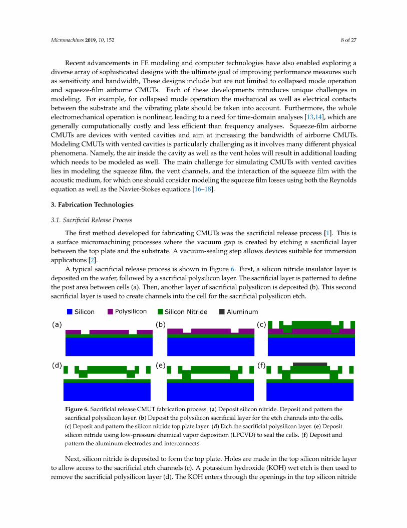
A typical sacrificial release process is shown in Figure 6. First, a silicon nitride insulator layer isdeposited on the wafer, followed by a sacrificial polysilicon layer. The sacrificial layer is patterned to definethe post area between cells (a). Then, another layer of sacrificial polysilicon is deposited (b). This secondsacrificial layer is used to create channels into the cell for the sacrificial polysilicon etch.
Figure 6. Sacrificial release CMUT fabrication process. (a) Deposit silicon nitride. Deposit and pattern thesacrificial polysilicon layer. (b) Deposit the polysilicon sacrificial layer for the etch channels into the cells.(c) Deposit and pattern the silicon nitride top plate layer. (d) Etch the sacrificial polysilicon layer. (e) Depositsilicon nitride using low-pressure chemical vapor deposition (LPCVD) to seal the cells. (f) Deposit andpattern the aluminum electrodes and interconnects.
Next, silicon nitride is deposited to form the top plate. Holes are made in the top silicon nitride layerto allow access to the sacrificial etch channels (c). A potassium hydroxide (KOH) wet etch is then used toremove the sacrificial polysilicon layer (d). The KOH enters through the openings in the top silicon nitride
Micromachines 2019, 10, 152 9 of 27
layer, then proceeds through the etch channels formed by the second sacrificial polysilicon deposition andinto the cells. KOH has high selectivity to polysilicon over silicon nitride, so the silicon nitride structureremains undamaged.
The sacrificial release step leaves a gap, which is vented to the atmosphere. The gap is sealed byperforming low-pressure chemical vapor deposition (LPCVD) of silicon nitride. This seals off the narrowetch channels (e). The LPCVD is performed at very low pressure, so the gap is effectively vacuum-filledwhen it is sealed.
Finally, aluminum is deposited to form the top electrode, electrical contacts, and interconnects (f).Sputtering is usually used in order to get conformal coverage. The substrate wafer is highly doped so thatit can be used as the back electrode.
In the sacrificial release process, the gap height is set by the combined thicknesses of the twopolysilicon depositions (a) and (b), and the top plate thickness is set by a silicon nitride deposition (c).This can make achieving good uniformity challenging compared to a wafer-bonding process. In addition,roughness in the silicon nitride layer can decrease the effective gap height, causing deviations in deviceperformance from the design values [19]. Also, the plate material can have substantial intrinsic stress,which alters the device properties.
On the other hand, sacrificial release processes have several advantages. They are relatively simpleand reliable. They avoid the yield challenges of a wafer bonding step. Additionally, it is possible to designsacrificial release processes with a low maximum processing temperature (250 °C) [20], allowing postprocessCMOS integration [21].
Vias and 2D Arrays
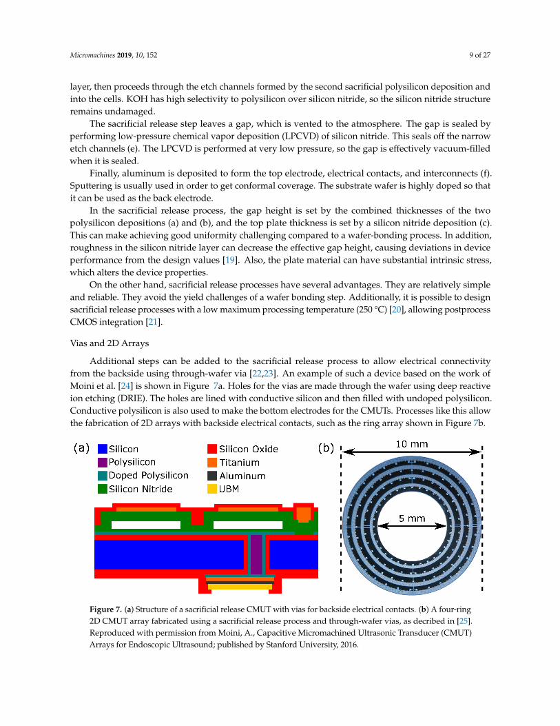
Additional steps can be added to the sacrificial release process to allow electrical connectivityfrom the backside using through-wafer via [22,23]. An example of such a device based on the work ofMoini et al. [24] is shown in Figure 7a. Holes for the vias are made through the wafer using deep reactiveion etching (DRIE). The holes are lined with conductive silicon and then filled with undoped polysilicon.Conductive polysilicon is also used to make the bottom electrodes for the CMUTs. Processes like this allowthe fabrication of 2D arrays with backside electrical contacts, such as the ring array shown in Figure 7b.
Figure 7. (a) Structure of a sacrificial release CMUT with vias for backside electrical contacts. (b) A four-ring2D CMUT array fabricated using a sacrificial release process and through-wafer vias, as decribed in [25].Reproduced with permission from Moini, A., Capacitive Micromachined Ultrasonic Transducer (CMUT)Arrays for Endoscopic Ultrasound; published by Stanford University, 2016.
Micromachines 2019, 10, 152 10 of 27
With backside electrical contacts, it is feasible to construct 2D arrays with individually-addressableelements. Rectangular 2D arrays have been fabricated for volumetric imaging [23], and ring arrays havebeen fabricated for forward-looking imaging on the ends of catheters [24].
3.2. Wafer Bonding—Basic Process
In this technique, a combination of surface micromachining and silicon on insulator (SOI) technologiesare used to fabricate the CMUT [26]. This wafer bonding process greatly simplifies the fabrication andbrings new levels of uniformity and control, especially regarding the plate thickness, which is now definedby the device layer of the SOI wafer.
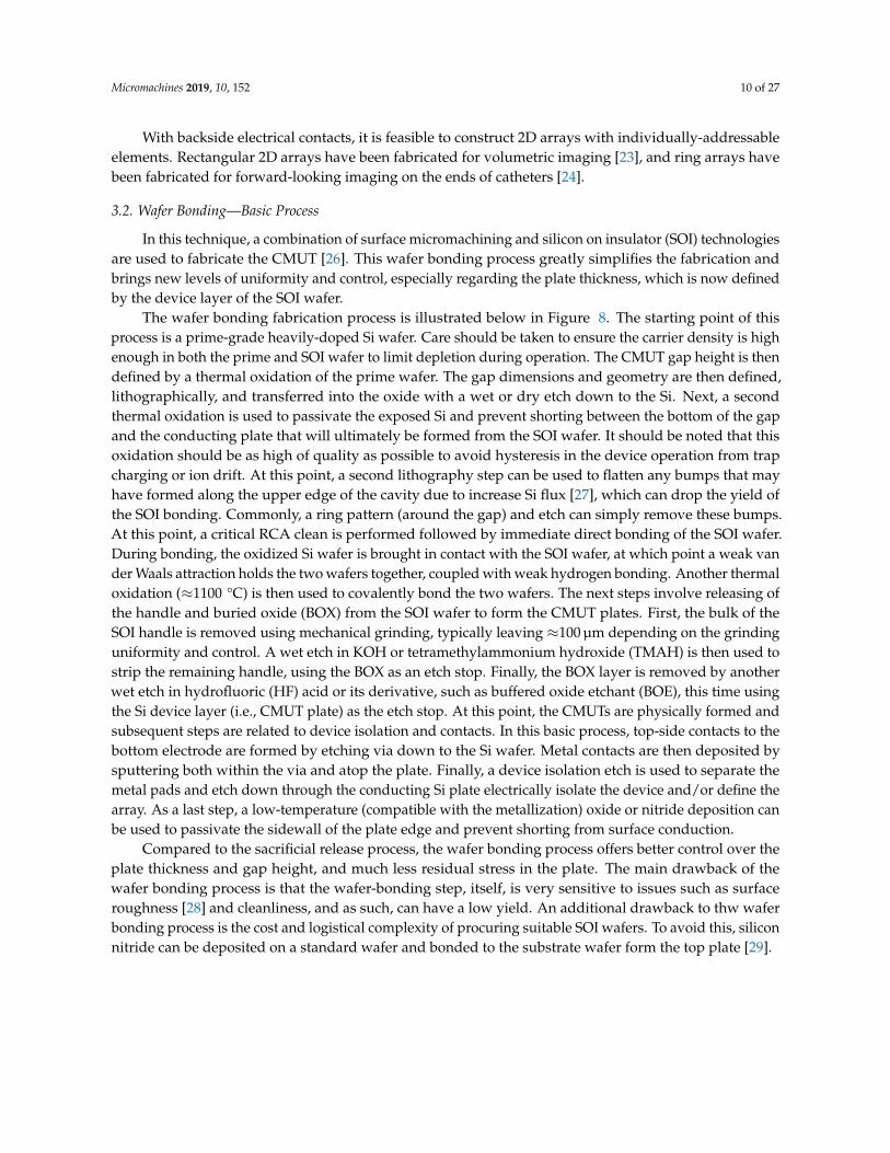
The wafer bonding fabrication process is illustrated below in Figure 8. The starting point of thisprocess is a prime-grade heavily-doped Si wafer. Care should be taken to ensure the carrier density is highenough in both the prime and SOI wafer to limit depletion during operation. The CMUT gap height is thendefined by a thermal oxidation of the prime wafer. The gap dimensions and geometry are then defined,lithographically, and transferred into the oxide with a wet or dry etch down to the Si. Next, a secondthermal oxidation is used to passivate the exposed Si and prevent shorting between the bottom of the gapand the conducting plate that will ultimately be formed from the SOI wafer. It should be noted that thisoxidation should be as high of quality as possible to avoid hysteresis in the device operation from trapcharging or ion drift. At this point, a second lithography step can be used to flatten any bumps that mayhave formed along the upper edge of the cavity due to increase Si flux [27], which can drop the yield ofthe SOI bonding. Commonly, a ring pattern (around the gap) and etch can simply remove these bumps.At this point, a critical RCA clean is performed followed by immediate direct bonding of the SOI wafer.During bonding, the oxidized Si wafer is brought in contact with the SOI wafer, at which point a weak vander Waals attraction holds the two wafers together, coupled with weak hydrogen bonding. Another thermaloxidation (≈1100 °C) is then used to covalently bond the two wafers. The next steps involve releasing ofthe handle and buried oxide (BOX) from the SOI wafer to form the CMUT plates. First, the bulk of theSOI handle is removed using mechanical grinding, typically leaving ≈100 µm depending on the grindinguniformity and control. A wet etch in KOH or tetramethylammonium hydroxide (TMAH) is then used tostrip the remaining handle, using the BOX as an etch stop. Finally, the BOX layer is removed by anotherwet etch in hydrofluoric (HF) acid or its derivative, such as buffered oxide etchant (BOE), this time usingthe Si device layer (i.e., CMUT plate) as the etch stop. At this point, the CMUTs are physically formed andsubsequent steps are related to device isolation and contacts. In this basic process, top-side contacts to thebottom electrode are formed by etching via down to the Si wafer. Metal contacts are then deposited bysputtering both within the via and atop the plate. Finally, a device isolation etch is used to separate themetal pads and etch down through the conducting Si plate electrically isolate the device and/or define thearray. As a last step, a low-temperature (compatible with the metallization) oxide or nitride deposition canbe used to passivate the sidewall of the plate edge and prevent shorting from surface conduction.
Compared to the sacrificial release process, the wafer bonding process offers better control over theplate thickness and gap height, and much less residual stress in the plate. The main drawback of thewafer bonding process is that the wafer-bonding step, itself, is very sensitive to issues such as surfaceroughness [28] and cleanliness, and as such, can have a low yield. An additional drawback to thw waferbonding process is the cost and logistical complexity of procuring suitable SOI wafers. To avoid this, siliconnitride can be deposited on a standard wafer and bonded to the substrate wafer form the top plate [29].
Micromachines 2019, 10, 152 11 of 27
Figure 8. Process flow for a wafer-bonded CMUT. (a) Starting prime wafer. (b) Thermal oxidation. (c) Etchto form cavity. (d) Thermal oxidation. (e) Silicon on insulator (SOI) wafer bonding. (f) SOI handle.(g) Removing burried oxide. (h) Sputtering metallization. (i) Metal pattern and device isolation.
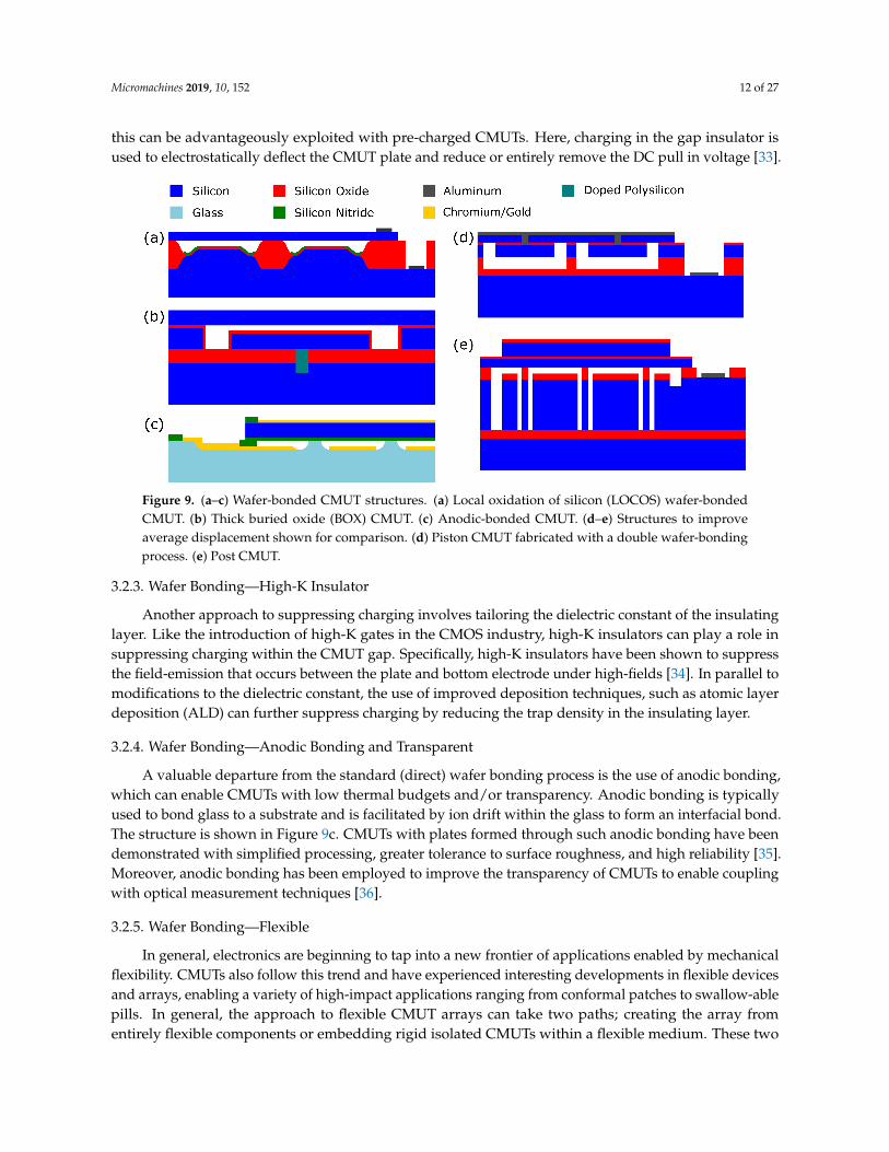
3.2.1. Wafer Bonding—LOCOS Process
The LOCOS (local oxidation of silicon) process is a variant of the wafer-bonding process that allowsexcellent gap height control and reduced parasitic capacitance when compared to the basic wafer bondingprocess [30]. The process uses local oxidation, a method used to isolate neighboring MOS transistors inwhich a silicon nitride mask is used to prevent the diffusion of oxidants to the silicon surface in particularlocations so that oxide only grows in specific areas.
A typical LOCOS CMUT structure is shown in Figure 9a. The elevated silicon area in the center ofthe cells is created using a local oxidation step. This step may be masked with silicon oxide [30] or siliconnitride [31]. A second LOCOS step produces the silicon oxide posts which support the top plate. In thisway, the gap height can be made small while keeping the post area thick, unlike the simple wafer bondingprocess where the gap height and post height are coupled. Gap heights as small as 40 nm have beenachieved using this process [30]. In the device shown in Figure 9a, there is no metal layer on the top plate.Instead, highly-doped silicon is used to provide conductivity.
3.2.2. Wafer Bonding—Thick BOX, Pre-Charged
A variety of modifications to the basic process flow for wafer-bonded CMUTs exist, each addressinga specific aspect of performance. Charging is one aspect of CMUT performance that has receivedconsiderable attention due to its impact on the device reliability. Specifically, charge trapping and ion driftin the insulating layer within the gap can be responsible for hysteresis in the electrostatic deflection of theplate. In response to such charging, the use of an SOI wafer with a thick BOX layer to form the bottomelectrodes has been proposed as one solution [32]. The structure is shown in Figure 9b. The purpose of thisis to localize the electrical field, which is the underlying cause of charging, to within the gap by patterningvias through the thick BOX layer. In addition, these backside contacts allow a flat and continuous front faceon the transducer array, which improves imaging and simplifies packaging. On the flip side of charging,
Micromachines 2019, 10, 152 12 of 27
this can be advantageously exploited with pre-charged CMUTs. Here, charging in the gap insulator isused to electrostatically deflect the CMUT plate and reduce or entirely remove the DC pull in voltage [33].
Figure 9. (a–c) Wafer-bonded CMUT structures. (a) Local oxidation of silicon (LOCOS) wafer-bondedCMUT. (b) Thick buried oxide (BOX) CMUT. (c) Anodic-bonded CMUT. (d–e) Structures to improveaverage displacement shown for comparison. (d) Piston CMUT fabricated with a double wafer-bondingprocess. (e) Post CMUT.
3.2.3. Wafer Bonding—High-K Insulator
Another approach to suppressing charging involves tailoring the dielectric constant of the insulatinglayer. Like the introduction of high-K gates in the CMOS industry, high-K insulators can play a role insuppressing charging within the CMUT gap. Specifically, high-K insulators have been shown to suppressthe field-emission that occurs between the plate and bottom electrode under high-fields [34]. In parallel tomodifications to the dielectric constant, the use of improved deposition techniques, such as atomic layerdeposition (ALD) can further suppress charging by reducing the trap density in the insulating layer.
3.2.4. Wafer Bonding—Anodic Bonding and Transparent
A valuable departure from the standard (direct) wafer bonding process is the use of anodic bonding,which can enable CMUTs with low thermal budgets and/or transparency. Anodic bonding is typicallyused to bond glass to a substrate and is facilitated by ion drift within the glass to form an interfacial bond.The structure is shown in Figure 9c. CMUTs with plates formed through such anodic bonding have beendemonstrated with simplified processing, greater tolerance to surface roughness, and high reliability [35].Moreover, anodic bonding has been employed to improve the transparency of CMUTs to enable couplingwith optical measurement techniques [36].
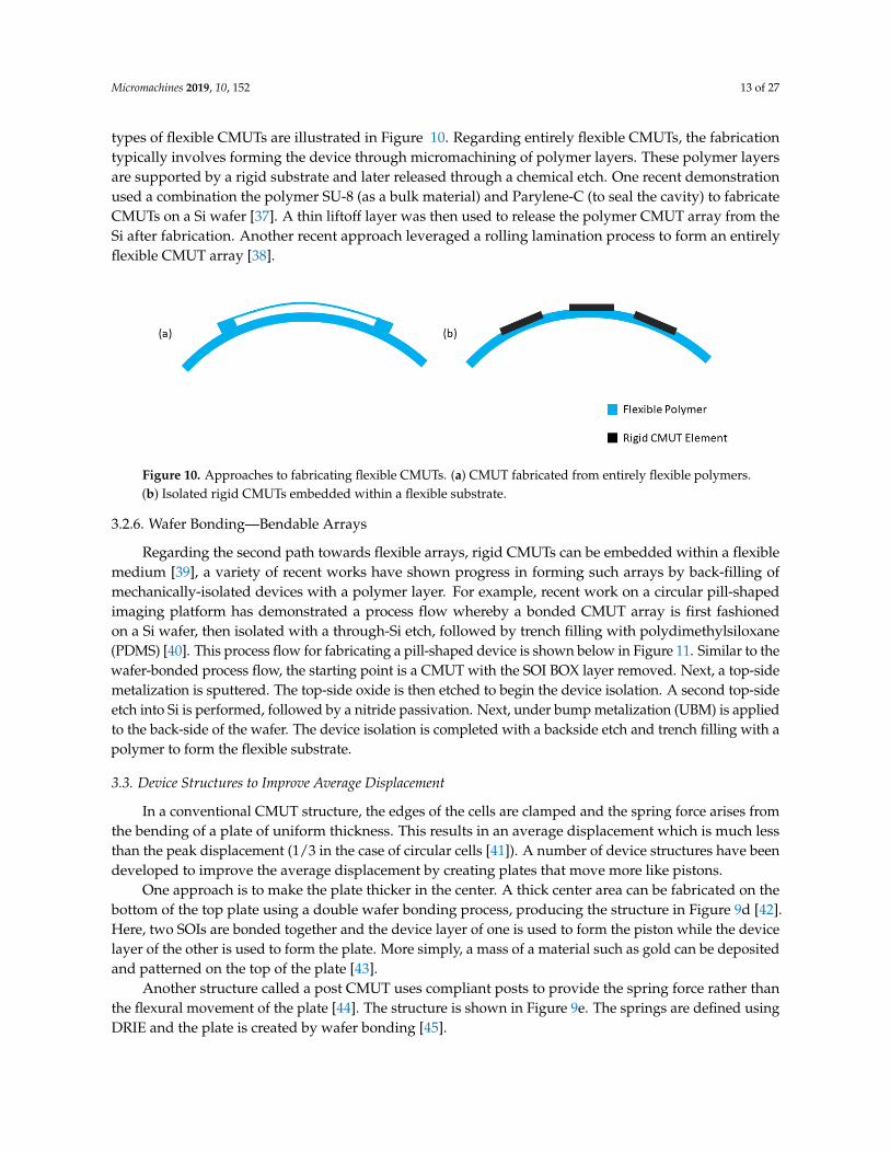
3.2.5. Wafer Bonding—Flexible
In general, electronics are beginning to tap into a new frontier of applications enabled by mechanicalflexibility. CMUTs also follow this trend and have experienced interesting developments in flexible devicesand arrays, enabling a variety of high-impact applications ranging from conformal patches to swallow-ablepills. In general, the approach to flexible CMUT arrays can take two paths; creating the array fromentirely flexible components or embedding rigid isolated CMUTs within a flexible medium. These two
Micromachines 2019, 10, 152 13 of 27
types of flexible CMUTs are illustrated in Figure 10. Regarding entirely flexible CMUTs, the fabricationtypically involves forming the device through micromachining of polymer layers. These polymer layersare supported by a rigid substrate and later released through a chemical etch. One recent demonstrationused a combination the polymer SU-8 (as a bulk material) and Parylene-C (to seal the cavity) to fabricateCMUTs on a Si wafer [37]. A thin liftoff layer was then used to release the polymer CMUT array from theSi after fabrication. Another recent approach leveraged a rolling lamination process to form an entirelyflexible CMUT array [38].
Figure 10. Approaches to fabricating flexible CMUTs. (a) CMUT fabricated from entirely flexible polymers.(b) Isolated rigid CMUTs embedded within a flexible substrate.
3.2.6. Wafer Bonding—Bendable Arrays
Regarding the second path towards flexible arrays, rigid CMUTs can be embedded within a flexiblemedium [39], a variety of recent works have shown progress in forming such arrays by back-filling ofmechanically-isolated devices with a polymer layer. For example, recent work on a circular pill-shapedimaging platform has demonstrated a process flow whereby a bonded CMUT array is first fashionedon a Si wafer, then isolated with a through-Si etch, followed by trench filling with polydimethylsiloxane(PDMS) [40]. This process flow for fabricating a pill-shaped device is shown below in Figure 11. Similar to thewafer-bonded process flow, the starting point is a CMUT with the SOI BOX layer removed. Next, a top-sidemetalization is sputtered. The top-side oxide is then etched to begin the device isolation. A second top-sideetch into Si is performed, followed by a nitride passivation. Next, under bump metalization (UBM) is appliedto the back-side of the wafer. The device isolation is completed with a backside etch and trench filling with apolymer to form the flexible substrate.
3.3. Device Structures to Improve Average Displacement
In a conventional CMUT structure, the edges of the cells are clamped and the spring force arises fromthe bending of a plate of uniform thickness. This results in an average displacement which is much lessthan the peak displacement (1/3 in the case of circular cells [41]). A number of device structures have beendeveloped to improve the average displacement by creating plates that move more like pistons.
One approach is to make the plate thicker in the center. A thick center area can be fabricated on thebottom of the top plate using a double wafer bonding process, producing the structure in Figure 9d [42].Here, two SOIs are bonded together and the device layer of one is used to form the piston while the devicelayer of the other is used to form the plate. More simply, a mass of a material such as gold can be depositedand patterned on the top of the plate [43].
Another structure called a post CMUT uses compliant posts to provide the spring force rather thanthe flexural movement of the plate [44]. The structure is shown in Figure 9e. The springs are defined usingDRIE and the plate is created by wafer bonding [45].
Micromachines 2019, 10, 152 14 of 27
Figure 11. Process flow for fabricating a bendable CMUT array. (a) A wafer-bonded CMUT after strippingthe SOI BOX. (b) Sputtering top-side metallization. (c) Top-side isolation etch. (d) Second top-side isolationwith nitride passivation. (e) Deposit of under bump metalization (UBM). (f) Secure to supporting wafer.(g) Back-side isolation and polydimethylsiloxane (PDMS) filling.
In addition to improving average displacement, the piston and post CMUTs decouple the complianceof the plate from the mass, which allows greater design flexibility. However, they both present fabricationchallenges. In the piston structure, any misalignment of the piston mass can change the dynamic behaviorof the cell. Fabrication of post CMUTs with high yield has proved complex and challenging [45].
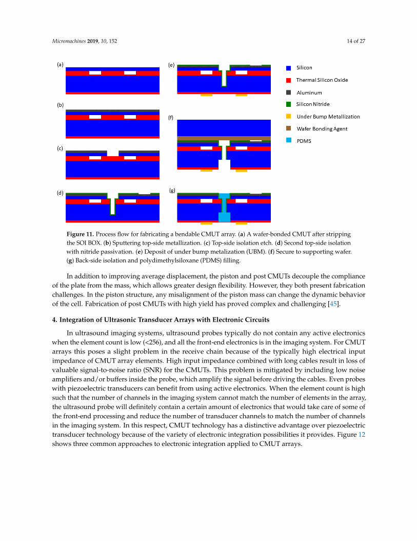
4. Integration of Ultrasonic Transducer Arrays with Electronic Circuits
In ultrasound imaging systems, ultrasound probes typically do not contain any active electronicswhen the element count is low (<256), and all the front-end electronics is in the imaging system. For CMUTarrays this poses a slight problem in the receive chain because of the typically high electrical inputimpedance of CMUT array elements. High input impedance combined with long cables result in loss ofvaluable signal-to-noise ratio (SNR) for the CMUTs. This problem is mitigated by including low noiseamplifiers and/or buffers inside the probe, which amplify the signal before driving the cables. Even probeswith piezoelectric transducers can benefit from using active electronics. When the element count is highsuch that the number of channels in the imaging system cannot match the number of elements in the array,the ultrasound probe will definitely contain a certain amount of electronics that would take care of some ofthe front-end processing and reduce the number of transducer channels to match the number of channelsin the imaging system. In this respect, CMUT technology has a distinctive advantage over piezoelectrictransducer technology because of the variety of electronic integration possibilities it provides. Figure 12shows three common approaches to electronic integration applied to CMUT arrays.
Micromachines 2019, 10, 152 15 of 27
Ultrasound Imaging
planarization layer
ASICUltrasound Imaging
ASIC
ASICUltrasound Imaging
flex−cablesflex−cables
(a)
(b)
(c)
CMUT array
flip−chip bonding
CMUT array
with through−wafer
interconnects
CMUT array
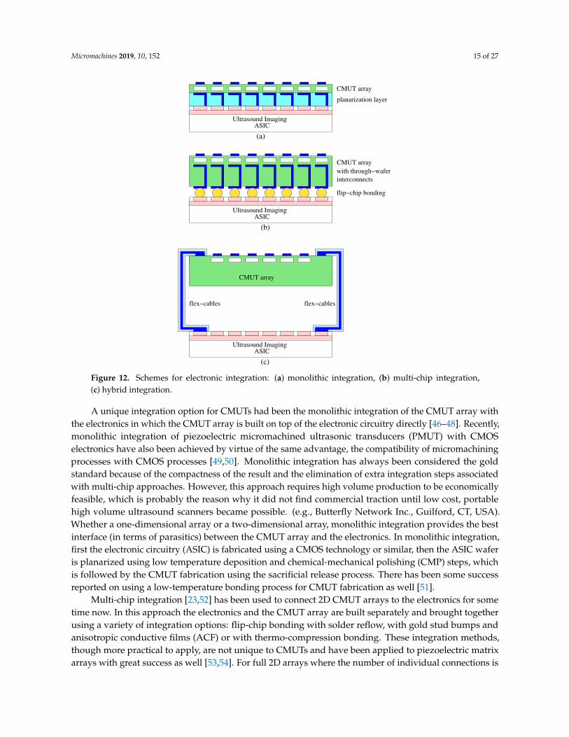
Figure 12. Schemes for electronic integration: (a) monolithic integration, (b) multi-chip integration,(c) hybrid integration.
A unique integration option for CMUTs had been the monolithic integration of the CMUT array withthe electronics in which the CMUT array is built on top of the electronic circuitry directly [46–48]. Recently,monolithic integration of piezoelectric micromachined ultrasonic transducers (PMUT) with CMOSelectronics have also been achieved by virtue of the same advantage, the compatibility of micromachiningprocesses with CMOS processes [49,50]. Monolithic integration has always been considered the goldstandard because of the compactness of the result and the elimination of extra integration steps associatedwith multi-chip approaches. However, this approach requires high volume production to be economicallyfeasible, which is probably the reason why it did not find commercial traction until low cost, portablehigh volume ultrasound scanners became possible. (e.g., Butterfly Network Inc., Guilford, CT, USA).Whether a one-dimensional array or a two-dimensional array, monolithic integration provides the bestinterface (in terms of parasitics) between the CMUT array and the electronics. In monolithic integration,first the electronic circuitry (ASIC) is fabricated using a CMOS technology or similar, then the ASIC waferis planarized using low temperature deposition and chemical-mechanical polishing (CMP) steps, whichis followed by the CMUT fabrication using the sacrificial release process. There has been some successreported on using a low-temperature bonding process for CMUT fabrication as well [51].
Multi-chip integration [23,52] has been used to connect 2D CMUT arrays to the electronics for sometime now. In this approach the electronics and the CMUT array are built separately and brought togetherusing a variety of integration options: flip-chip bonding with solder reflow, with gold stud bumps andanisotropic conductive films (ACF) or with thermo-compression bonding. These integration methods,though more practical to apply, are not unique to CMUTs and have been applied to piezoelectric matrixarrays with great success as well [53,54]. For full 2D arrays where the number of individual connections is
Micromachines 2019, 10, 152 16 of 27
very high, fanning out interconnects to the sides where conventional interconnect schemes (wire bonding)can be used become impractical. In that case, flip-chip bonding the 2D CMUT array onto the electronicsbecomes a necessity. The amount of electronic integration that can be incorporated into a CMUT probevaries depending on many parameters, ranging from size to power consumption to the type of application.We will now look into some of these varieties and their associated electronics.
4.1. Analog Front End Integration for SNR Improvement
CMUTs typically have higher electrical input impedance and suffer from the parasitic capacitance ofthe interconnection between the transducer array and the system more than piezoelectric transducer arraysdo. To alleviate this problem, a simple solution has been proposed and implemented. An array of low noisepreamplifiers is integrated into the probe. The preamplifiers are equipped with active or passive switches thatisolate them from the transmit circuitry during high voltage transmit events. After the transmit event theswitches change position and the received signals go through the low noise preamplifiers. These amplifiersneed not have high amplification but should be low noise and be able to drive the low impedance of the cableand the system front end [55]. Such preamplifiers have already been implemented on standard US front-endchip sets [56]. To accommodate the high input impedance of the CMUT elements, high input impedancepreamplifiers can be used. When accompanied with buffers high input impedance preamplifiers reduce signalloss due to the loading of the system cables. However, these preamplifiers are still susceptible to parasiticcapacitances between the preamplifier and the transducer element. In case of high parasitic capacitancein the CMUT element and between the CMUT element and the preamplifier, transimpedance amplifiers(aka resistive feedback amplifiers) provide an elegant solution by creating a low impedance node at thepreamplifier input which essentially shunts the parasitic capacitance. Both these approaches provide goodsolutions with some gain and wide bandwidth. Another approach is to use capacitive feedback preamplifiers.These amplifiers are similar to transimpedance amplifiers where the feedback resistor is replaced by a feedbackcapacitor. Because the impedance of the capacitor drops with frequency, these amplifier show low-passbehavior and are somewhat band-limited. On the other hand, because the feedback resistor is eliminated,capacitive feedback amplifiers show excellent noise performance [57].
4.2. Row-Column Addressing
Row-column addressed CMUTs have found a renewed interest in recent years. The row-columnaddressing allows the fabrication of 2D CMUT arrays relatively easily with reduced number ofinterconnects [46,58,59]. In this type of array, the bottom electrode is divided into lines (as opposedto making the whole silicon substrate a single electrode which is typically the case for 1D arrays). The topelectrode on the other hand is also divided into lines that are perpendicular to the bottom electrodelines. The intersection of these perpendicular lines, which we can refer to as azimuth and elevationlines, constitute an element of the 2D array. Each element in the array is accessed by accessing thecorresponding row and column electrodes. Hence, only 2N connections are required, rather than N2 toaccess all the elements. The electronics associated with row-column addressed CMUTs can be somewhatmore complicated than the front-end electronics for one-dimensional arrays depending on how they areimplemented, but they are a lot simpler than that of fully addressable 2D arrays and produce volumetricimages. Hence, row-column addressed 2D CMUT arrays present a very attractive alternative to fullyaddressable 2D arrays. A row-column addressed 2D array can be used as a synthetic 1D array whoseelevation aperture is dynamically changed and electronically scanned in the elevation direction. In thisscenario the azimuth lines are connected to the system channels directly whereas the elevation lines areconnected to the bias voltage(s) through switches. By electronically turning on and off the switches theelevation aperture is adjusted for each firing [60–62]. Another approach is to switch the elevation and
Micromachines 2019, 10, 152 17 of 27
azimuth apertures between transmit and receive events while applying Fresnel focusing in the elevationdirection, which provides isotropic resolution in azimuth and elevation directions [46]. In such systems, aswitch matrix is used to selectively connect each azimuth and elevation line to a system channel, to thebias voltage or to ground. Such a switch matrix can be integrated in any one of the ways described above.
4.3. Catheter Based Imaging Systems
CMUTs have catalyzed considerable progress in catheter based imaging applications where array sizeand channel count are severely limited due to physical constraints such as blood vessel diameter. CMUTs offerelegant solutions to the array size problem. The fabrication flexibility allows manufacturing of small, highfrequency, linear, ring shaped, cylindrical forward looking and side looking arrays. Small element size andthe long cables associated with catheters warrant a higher level of electronic integration at the catheter tipeven for piezoelectric transducers, and only more so for CMUTs. The electronic integration options discussedabove along with fabrication simplicity makes CMUTs a better option for catheter based imaging systems.To overcome the parasitic capacitance that the cables present CMUTs are integrated with low noise amplifiersand buffers [21,24,63,64]. The size constraint also limits the number of cables that can run through a catheter.Hence, reducing the number of channels becomes a necessity. Analog multiplexing of the transducer channelsand applying synthetic aperture imaging can reduce the number of connections to as low as two [65] withsome compromise in the imaging quality and frame rate. A more efficient approach is to integrate TXbeamformers and analog multiplexers with the CMUT array at the catheter tip to reduce the cable countwithout compromising the image quality [48,66,67].
4.4. Imaging System on a Chip
Developments in the electronics industry have opened up the way to building ultrasound imagingsystems on a chip. Combined with post processing methods to fabricate CMUTs, it is now possible to buildsingle chip ultrasound imaging systems. One caveat in this approach is that ultrasound imaging typicallyinvolves a very large dynamic range. Transmit voltages and CMUT DC bias voltages are typically highvoltages (≈100 V), whereas received signals are very low voltages. Maintaining a high signal-to-noise ratioand frequency bandwidth is probably the most important objective in the receive chain. In addition, thereis the digital component of the imaging system. Combining all of these in a single chip provides the bestsignal integrity but may compromise signal quality to some degree. However, HV-BCD processes seemsto overcome such problems [57,67,68]. Building ultrasound imaging systems on a chip or even on multiplechips paves the way to very low cost, ultra portable ultrasound imaging systems. When combined withtoday’s wireless communication capabilities and battery power technologies, such ultrasound systemsturn into flexible, wearable, ingestible standalone ultrasound imaging systems. In our group we havedeveloped and demonstrated the components of such a system which would go into an ingestible capsuleform and provide the images of the gastrointestinal tract. This capsule combines an ultrasound imagingsystem with on-chip transmit and receive beamforming capability, with power management and wirelesstransfer circuitry [69,70]. The system acquires US images of the intestinal cross-section and wirelesslytransmits them to a host computer Figure 13. In addition to the high dynamic range requirements, the formfactor of an ingestible US imaging system forces a multichip approach for this integration problem.
4.5. Imaging and HIFU System Integration
CMUTs have two very distinctive advantages when it comes to high intensity focused ultrasound(HIFU) applications. One of them is the ability to do imaging and HIFU with the same transducerarray given the inherent wide frequency band of the CMUT transducers. The other one is the lackof a self-heating mechanism in CMUTs (whereas for piezoelectric transducers self heating is the main

Micromachines 2019, 10, 152 18 of 27
issue). Therefore, CMUT transducer arrays are excellent candidates for dual mode operation. Dual modeoperation usually requires specific electronic circuitry that interfaces the HIFU drivers with the transducerarrays. In HIFU operation long bursts of sinusoidal signals are used to excite the elements. The pulsersin the imaging circuitry are usually not efficient enough to generate such kind of long bursts withoutoverheating, and therefore separate HIFU drivers are needed for dual mode operation. The HIFU driver isinterfaced to the CMUT array and the imaging system with a switch matrix which switches from imagingto HIFU and back to imaging in a programmable manner to be able to ablate tissue and monitor theresults in real time. In our group we have successfully developed and demonstrated such a dual modeimaging/HIFU system for ablation in shallow tissue that uses a 2D CMUT array which is flip-chip bondedto the electronic circuitry [71,72]. The 2D CMUT array consists of dedicated transmit and receive elements.The transmit elements are connected to a TX beamformer whereas the receive elements are connected to lownoise receive amplifiers. To reduce power consumption in the ASIC, an off-chip, standalone, eight-channelHIFU driver is used. The ASIC includes high-voltage switches to switch the TX elements between imagingpulsers and HIFU channels Figure 14. With this integrated device, it is possible to do HIFU (up to 16 MPapeak to peak pressure at 1 cm focal depth at 5 MHz) and imaging with the same 2D array. As the levelof electronic integration increases thermal management of the transducer array and electronics assemblystart to become an important issue, especially in dual mode systems. For example, even though off-chipHIFU drivers are used the amount of power dissipation in the high-voltage switches in the ASIC is enoughto increase the probe temperature to unacceptable levels (42 °C US probes). However, the thermal energylevels involved are modest and is easily managed by basic thermal design considerations.
Figure 13. Capsule US imaging system.
Imaging
Pulser
HIFU
Driver
TX elements
RX elements
TIA Buffer
HV Switch
TX
Beamformer
ASIC Chip
FPGA
System
Figure 14. Dual-mode high intensity focused ultrasound (HIFU) and imaging system with 2D CMUT arrayand electronic circuitry (ASIC).
Micromachines 2019, 10, 152 19 of 27
5. Applications
As there have already been many applications of CMUTs, we cannot present them all here.Instead, we have selected applications of particular interest from our own work.
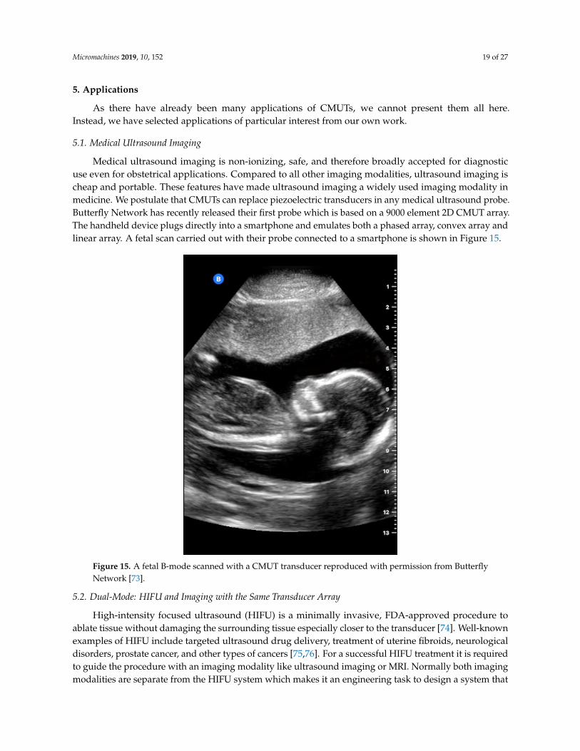
5.1. Medical Ultrasound Imaging
Medical ultrasound imaging is non-ionizing, safe, and therefore broadly accepted for diagnosticuse even for obstetrical applications. Compared to all other imaging modalities, ultrasound imaging ischeap and portable. These features have made ultrasound imaging a widely used imaging modality inmedicine. We postulate that CMUTs can replace piezoelectric transducers in any medical ultrasound probe.Butterfly Network has recently released their first probe which is based on a 9000 element 2D CMUT array.The handheld device plugs directly into a smartphone and emulates both a phased array, convex array andlinear array. A fetal scan carried out with their probe connected to a smartphone is shown in Figure 15.
Figure 15. A fetal B-mode scanned with a CMUT transducer reproduced with permission from ButterflyNetwork [73].
5.2. Dual-Mode: HIFU and Imaging with the Same Transducer Array
High-intensity focused ultrasound (HIFU) is a minimally invasive, FDA-approved procedure toablate tissue without damaging the surrounding tissue especially closer to the transducer [74]. Well-knownexamples of HIFU include targeted ultrasound drug delivery, treatment of uterine fibroids, neurologicaldisorders, prostate cancer, and other types of cancers [75,76]. For a successful HIFU treatment it is requiredto guide the procedure with an imaging modality like ultrasound imaging or MRI. Normally both imagingmodalities are separate from the HIFU system which makes it an engineering task to design a system that

Micromachines 2019, 10, 152 20 of 27
guarantees co-registration between the HIFU delivery location with the imaging. Here we present a devicewhere we have combined the imaging and HIFU system into one integrated circuit (IC) that operates onone 32 × 32 element 2D CMUT array and the co-registration is therefore an integral part of the system.The IC can switch between HIFU mode and imaging mode on a millisecond scale giving the illusion to theuser that the HIFU ablation and imaging is taking place at the same time. The switching time is limited bythe speed of the DC power supplies. The dual-mode device is shown in Figure 16.
(a)
(b) (c)Figure 16. (a) The integrated CMUT, IC and flexible printed circuit board (flex PCB) prior to PDMS casting.(b) 3D imaging result of a wire phantom. (c) HIFU ablation of a piece of ex-vivo tissue. All images from [71].Reproduced with permission from Jang, J.H. et al., 2015 IEEE International Ultrasonics Symposium (IUS);published by IEEE Xplore, 2015 [72]. Reproduced with permission from Jang, J.H. et al., 2017 IEEEInternational Ultrasonics Symposium (IUS); published by IEEE Xplore, 2017.
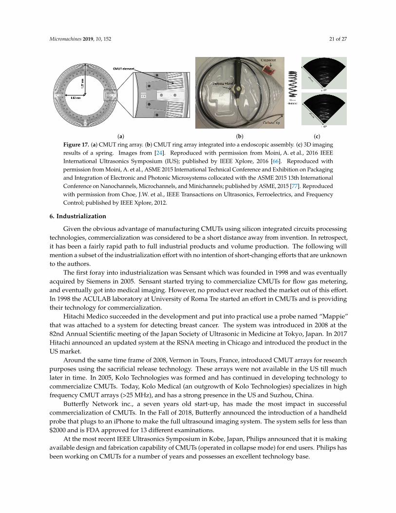
5.3. Catheter Based Ultrasound Imaging
An alternative to an imaging and HIFU system that operates as one, is to have a system that easesthe coupling between the two systems and therefore also the co-registration. We present here a CMUTring array that has been fully integrated into a catheter assembly with a 12.5 mm OD and 4 mm ID.The circular catheter form-factor makes it easy to couple and co-register the imaging array with acenter-piece, see Figure 17a, HIFU system or optical fibers for photoacoustic imaging. The catheteris shown in Figure 17.
Micromachines 2019, 10, 152 21 of 27
(a) (b) (c)Figure 17. (a) CMUT ring array. (b) CMUT ring array integrated into a endoscopic assembly. (c) 3D imagingresults of a spring. Images from [24]. Reproduced with permission from Moini, A. et al., 2016 IEEEInternational Ultrasonics Symposium (IUS); published by IEEE Xplore, 2016 [66]. Reproduced withpermission from Moini, A. et al., ASME 2015 International Technical Conference and Exhibition on Packagingand Integration of Electronic and Photonic Microsystems collocated with the ASME 2015 13th InternationalConference on Nanochannels, Microchannels, and Minichannels; published by ASME, 2015 [77]. Reproducedwith permission from Choe, J.W. et al., IEEE Transactions on Ultrasonics, Ferroelectrics, and FrequencyControl; published by IEEE Xplore, 2012.
6. Industrialization
Given the obvious advantage of manufacturing CMUTs using silicon integrated circuits processingtechnologies, commercialization was considered to be a short distance away from invention. In retrospect,it has been a fairly rapid path to full industrial products and volume production. The following willmention a subset of the industrialization effort with no intention of short-changing efforts that are unknownto the authors.
The first foray into industrialization was Sensant which was founded in 1998 and was eventuallyacquired by Siemens in 2005. Sensant started trying to commercialize CMUTs for flow gas metering,and eventually got into medical imaging. However, no product ever reached the market out of this effort.In 1998 the ACULAB laboratory at University of Roma Tre started an effort in CMUTs and is providingtheir technology for commercialization.
Hitachi Medico succeeded in the development and put into practical use a probe named “Mappie”that was attached to a system for detecting breast cancer. The system was introduced in 2008 at the82nd Annual Scientific meeting of the Japan Society of Ultrasonic in Medicine at Tokyo, Japan. In 2017Hitachi announced an updated system at the RSNA meeting in Chicago and introduced the product in theUS market.
Around the same time frame of 2008, Vermon in Tours, France, introduced CMUT arrays for researchpurposes using the sacrificial release technology. These arrays were not available in the US till muchlater in time. In 2005, Kolo Technologies was formed and has continued in developing technology tocommercialize CMUTs. Today, Kolo Medical (an outgrowth of Kolo Technologies) specializes in highfrequency CMUT arrays (>25 MHz), and has a strong presence in the US and Suzhou, China.
Butterfly Network inc., a seven years old start-up, has made the most impact in successfulcommercialization of CMUTs. In the Fall of 2018, Butterfly announced the introduction of a handheldprobe that plugs to an iPhone to make the full ultrasound imaging system. The system sells for less than$2000 and is FDA approved for 13 different examinations.
At the most recent IEEE Ultrasonics Symposium in Kobe, Japan, Philips announced that it is makingavailable design and fabrication capability of CMUTs (operated in collapse mode) for end users. Philips hasbeen working on CMUTs for a number of years and possesses an excellent technology base.
Micromachines 2019, 10, 152 22 of 27
Similarly, the Fraunhofer Institute for Photonoic Microsystems (IPMS) has been working on CMUTsand is commercializing CMUTs for a number of applications both in the medical space and in airborneultrasound. IPMS has a previous history in making vibrating ribbons for light modulation (silicon lightvalve), a device that is very similar to the CMUT in design and construction.
Another player in the space is Canon, which has been working on 3D real time photoacoustic imagingsystems for breast screening using 2D arrays of CMUTs. It is expected that they will be on the market withsuch systems once they receive FDA approval.
Overall, it is estimated that there is a total of about 23 companies offering CMUT products.
7. Discussion
Since its inception 25 years ago, CMUT technology have seen significant developments, especially inthe last decade. With the advance of the modern modeling tools, both analytical and numerical CMUTmodels have become accurate and reliable enough to make industrial quality designs possible both fornormal mode and collapse mode of operation. Fabrication processes and electronic integration toolshave also matured to the point that mass production of CMUT probes along with its accompanyingelectronics have become economically feasible. As a result, more and more ultrasound imaging companieshave started to incorporate CMUT probes into their systems. The ease of miniaturization and variety ofelectronic integration options enabled low-cost, ultra-portable, wireless or with minimal wiring, wearableor ingestible complete ultrasound imaging systems possible.
CMUTs show distinctive advantages when it comes to high intensity focused ultrasound applications.The lack of self-heating mechanism and inherent wide frequency bandwidth make CMUTs an excellentcandidate for HIFU and dual mode imaging/HIFU applications. Although this option hasn’t seen acommercial application yet, primarily because it is an area that is being explored only recently, there hasbeen successful demonstrations of dual mode operation with CMUTs. The future work on CMUTs islikely to include its therapeutic uses as well. Some imaging systems have already started including HIFUcapability which should find commercial success in the coming years.
Funding: This research was funded by the NIH grant number 1R01EB023901.
Acknowledgments: The authors would like to thank Soitec for kindly sponsoring SOI wafers used for CMUTfabrication in different projects by our group.
Conflicts of Interest: B.T. Khuri–Yakub serves as a technical advisor for Butterfly Network. The other authors declareno conflict of interest.
References
1. Haller, M.I.; Khuri-Yakub, B.T. A Surface Micromachined Electrostatic Ultrasonic Air Transducer. IEEE Trans.Ultrason. Ferroelectr. Freq. Control 1996, 43, 1–6. [CrossRef]
2. Soh, H.T.; Ladabaum, I.; Atalar, A.; Quate, C.F.; Khuri-Yakub, B.T. Silicon micromachined ultrasonic immersiontransducers. Appl. Phys. Lett. 1996, 69, 3674–3676. [CrossRef]
3. Park, K.K.; Oralkan, O.; Khuri-Yakub, B. A comparison between conventional and collapse-mode capacitivemicromachined ultrasonic transducers in 10-MHz 1-D arrays. IEEE Trans. Ultrason. Ferroelectr. Freq. Control 2013,60, 1245–1255. [CrossRef] [PubMed]
4. Mason, W.P. Electromechanical Transducers and Wave Filters; D. Van Nostrand: New York, NY, USA, 1942.5. Ladabaum, I.; Jin, X.; Soh, H.; Atalar, A.; Khuri-Yakub, B. Surface micromachined capacitive ultrasonic
transducers. IEEE Trans. Ultrason. Ferroelectr. Freq. Control 1998, 45, 678–690. [CrossRef] [PubMed]6. Khuri-yakub, B.T.; Cheng, C.H.; Degertekin, F.L.; Ergun, S.; Hansen, S.; Jin, X.; Oralkan, O. Silicon Micromachined
Ultrasonic Transducers. Jpn. J. Appl. Phys. 2000, 39, 2883–2887. [CrossRef]

Micromachines 2019, 10, 152 23 of 27
7. Nikoozadeh, A.; Bayram, B.; Yaralioglu, G.; Khuri-Yakub, B. Analytical calculation of collapse voltage of CMUTmembrane. In Proceedings of the IEEE Ultrasonics Symposium, Montreal, QC, Canada, 23–27 August 2004;Volume 1, pp. 256–259. [CrossRef]
8. Lohfink, A.; Eccardt, P.C.; Benecke, W.; Meixner, H. Derivation of a 1D CMUT model from FEM results for linearand nonlinear equivalent circuit simulation. In Proceedings of the IEEE Symposium on Ultrasonics, Honolulu,HI, USA, 5–8 October 2003; pp. 465–468. [CrossRef]
9. Lohfink, A.; Eccardt, P.C. Linear and nonlinear equivalent circuit modeling of CMUTs. IEEE Trans. Ultrason.Ferroelectr. Freq. Control 2005, 52, 2163–2172. [CrossRef] [PubMed]
10. Morse, P.M.P.M.; Ingard, K.U. Theoretical Acoustics; Princeton University Press: Princeton, NJ, USA, 1986; p. 927.11. Yaralioglu, G.; Ergun, S.; Khuri-Yakub, B. Finite-element analysis of capacitive micromachined ultrasonic
transducers. IEEE Trans. Ultrason. Ferroelectr. Freq. Control 2005, 52, 2185–2198. [CrossRef] [PubMed]12. Kupnik, M.; Wygant, I.O.; Khuri-Yakub, B.T. Finite element analysis of stress stiffening effects in CMUTS.
In Proceedings of the 2008 IEEE Ultrasonics Symposium, Beijing, China, 2–5 November 2008; pp. 487–490.[CrossRef]
13. Bayram, B.; Yaralioglu, G.; Kupnik, M.; Ergun, A.; Oralkan, O.; Nikoozadeh, A.; Khuri-Yakub, B.Dynamic analysis of capacitive micromachined ultrasonic transducers. IEEE Trans. Ultrason. Ferroelectr.Freq. Control 2005, 52, 2270–2275. [CrossRef] [PubMed]
14. Khuri-Yakub, B.T.; Yaralioglu, G.G.; Bayram, B. 5F-3 Finite Element Analysis of CMUTS: Conventional vs.Collapse Operation Modes. In Proceedings of the 2006 IEEE Ultrasonics Symposium, Vancouver, BC, Canada,2–6 October 2006; pp. 586–589. [CrossRef]
15. Jackson, J.D. Classical Electrodynamics, 3rd ed.; Wiley: Hoboken, NJ, USA, 1999; p. 808.16. Apte, N.; Park, K.K.; Khuri-Yakub, B.T. Finite element analysis of CMUTs with pressurized cavities.
In Proceedings of the 2012 IEEE International Ultrasonics Symposium, Dresden, Germany, 7–10 October 2012;pp. 979–982. [CrossRef]
17. Apte, N.; Park, K.K.; Nikoozadeh, A.; Khuri-Yakub, B.T. Bandwidth and sensitivity optimization in CMUTs forairborne applications. In Proceedings of the 2014 IEEE International Ultrasonics Symposium, Chicago, IL, USA,3–6 September 2014; pp. 166–169. [CrossRef]
18. Ma, B.; Chang, C.; Oguz, H.K.; Firouzi, K.; Khuri-Yakub, B.T.; Lab, E.L.G. Multi-parameter optimization ofvented CMUTs for airborne applications. In Proceedings of the 2017 IEEE International Ultrasonics Symposium(IUS), Washington, DC, USA, 6–9 September 2017; pp. 1–4. [CrossRef]
19. Lin, D.S.; Zhuang, X.; Wong, S.H.; Ergun, A.S.; Kupnik, M.; Khuri-Yakub, B.T. Characterization of fabricationrelated gap-height variations in capacitive micromachined ultrasonic transducers. In Proceedings of the IEEEUltrasonics Symposium, New York, NY, USA, 28–31 October 2007. [CrossRef]
20. Knight, J.; McLean, J.; Degertekin, F.L. Low temperature fabrication of immersion capacitive micromachinedultrasonic transducers on silicon and dielectric substrates. IEEE Trans. Ultrason. Ferroelectr. Freq. Control 2004, 51,1324–1333. [CrossRef]
21. Zahorian, J.; Hochman, M.; Xu, T.; Satir, S.; Gurun, G.; Karaman, M.; Degertekin, F.L. Monolithic CMUT-on-CMOSintegration for intravascular ultrasound applications. IEEE Trans. Ultrason. Ferroelectr. Freq. Control 2011,58, 2659–2667. [CrossRef] [PubMed]
22. Cheng, C.H.; Chow, E.M.; Jin, X.; Ergun, S.; Khuri-Yakub, B.T. An Efficient Electrical Addressing MethodUsing Through-Wafer Vias for Two-Dimensional Ultrasonic Arrays. In Proceedings of the IEEE InternationalUltrasonics Symposium (IUS), San Juan, PR, USA, 22–25 October 2000; pp. 1179–1182.
23. Wygant, I.O.; Zhuang, X.; Yeh, D.T.; Oralkan, O.; Ergun, A.S.; Karaman, M.; Khuri-Yakub, B.T. Integration of 2DCMUT arrays with front-end electronics for volumetric ultrasound imaging. IEEE Trans. Ultrason. Ferroelectr.Freq. Control 2008, 55, 327–342. [CrossRef] [PubMed]
24. Moini, A.; Nikoozadeh, A.; Choe, J.W.; Chang, C.; Stephens, D.N.; Sahn, D.J.; Khuri-Yakub, P.T. Fully integrated 2DCMUT ring arrays for endoscopic ultrasound. In Proceedings of the IEEE International Ultrasonics Symposium (IUS),Tours, France, 18–21 September 2016; pp. 3–6. [CrossRef]
Micromachines 2019, 10, 152 24 of 27
25. Moini, A. Capacitive Micromachined Ultrasonic Transducer (CMUT) Arrays for Endoscopic Ultrasound.Ph.D. Thesis, Stanford University, Stanford, CA, USA, 2016.
26. Huang, Y.; Ergun, A.S.; Haeggstrom, E.; Khuri-Yakub, B.T. Fabrication of Capacitive Micromachined UltrasonicTransducers (CMUTs) Using Wafer Bonding Technology for Low Frequency (10 kHz–150 kHz) Sonar Applications.In Proceedings of the IEEE Oceans, Biloxi, MI, USA, 29–31 October 2002; pp. 2322–2327.
27. Sarioglu, A.F.; Kupnik, M.; Vaithilingam, S.; Khuri-Yakub, B.T. Nanoscale Topography of Thermally-GrownOxide Films at Right-Angled Convex Corners of Silicon. J. Electrochem. Soc. 2011, 159, H79–H84. [CrossRef]
28. Miki, N.; Spearing, S.M. Effect of nanoscale surface roughness on the bonding energy of direct-bonded siliconwafers. J. Appl. Phys. 2003, 94, 6800–6806. [CrossRef]
29. Logan, A.; Yeow, J.T.W. Fabricating capacitive micromachined ultrasonic transducers with a novelsilicon-nitride-Based wafer bonding process. IEEE Trans. Ultrason. Ferroelectr. Freq. Control 2009, 56, 1074–1084.[CrossRef] [PubMed]
30. Park, K.K.; Lee, H.; Kupnik, M.; Khuri-Yakub, B.T. Fabrication of capacitive micromachined ultrasonictransducers via local oxidation and direct wafer bonding. J. Microelectromech. Syst. 2011, 20, 95–103. [CrossRef]
31. Molgaard, M.J.; Hansen, J.M.; Jakobsen, M.H.; Thomsen, E.V. Sensitivity Optimization of Wafer BondedGravimetric CMUT Sensors. J. Microelectromech. Syst. 2018, 7, 1089–1096. [CrossRef]
32. Kupnik, M.; Vaithilingam, S.; Torashima, K.; Wygant, I.O.; Khuri-Yakub, B.T. CMUT fabrication based on a thickburied oxide layer. In Proceedings of the IEEE Ultrasonics Symposium, San Diego, CA, USA, 11–14 October 2010.[CrossRef]
33. Ho, M.C.; Kupnik, M.; Park, K.K.; Khuri-Yakub, B.T. Long-term measurement results of pre-charged CMUTs withzero external bias operation. In Proceedings of the IEEE International Ultrasonics Symposium (IUS), Dresden,Germany, 7–10 October 2012. [CrossRef]
34. Xu, T.; Tekes, C.; Degertekin, F. CMUTs with high-K atomic layer deposition dielectric material insulation layer.IEEE Trans. Ultrason. Ferroelectr. Freq. Control 2014, 61, 2121–2131. [CrossRef] [PubMed]
35. Yamaner, F.Y.; Zhang, X.; Oralkan, O. A three-mask process for fabricating vacuum-sealed capacitivemicromachined ultrasonic transducers using anodic bonding. IEEE Trans. Ultrason. Ferroelectr. Freq. Control 2015,62, 972–982. [CrossRef] [PubMed]
36. Zhang, X.; Adelegan, O.; Yamaner, F.Y.; Oralkan, O. CMUTs on glass with ITO bottom electrodes forimproved transparency. In Proceedings of the IEEE International Ultrasonics Symposium (IUS), Tours, France,18–21 September 2016. [CrossRef]
37. Gerardo, C.D.; Cretu, E.; Rohling, R. Fabrication and testing of polymer-based capacitive micromachinedultrasound transducers for medical imaging. Microsyst. Nanoeng. 2018, 4, 19. [CrossRef]
38. Pang, D.C.; Chang, C.M. Development of a novel transparent flexible capacitive micromachined ultrasonictransducer. Sensors 2017, 17, 1443. [CrossRef] [PubMed]
39. Zhuang, X.; Lin, D.S.; Oralkan, O.; Khuri-Yakub, B.T. Fabrication of flexible transducer arrays with through-waferelectrical interconnects based on trench refilling with PDMS. J. Microelectromechan. Syst. 2008, 17, 446–452.[CrossRef]
40. Wang, J.; Memon, F.; Touma, G.; Baltsavias, S.; Jang, J.H.; Chang, C.; Rasmussen, M.F.; Olcott, E.; Jeffrey, R.B.;Arbabian, A.; et al. Capsule ultrasound device: Characterization and testing results. In Proceedings of the2017 IEEE International Ultrasonics Symposium (IUS), Washington, DC, USA, 6–9 September 2017; pp. 1–4.[CrossRef]
41. Wygant, I.O.; Kupnik, M.; Khuri-Yakub, B.T. Analytically Calculating Membrane Displacement and theEquivalent Circuit Model of a Circular CMUT Cell. In Proceedings of the IEEE International UltrasonicsSymposium (IUS), Beijing, China, 2–5 November 2008; pp. 2111–2114.
42. Huang, Y.; Zhuang, X.; Hæggstrom, E.O.; Ergun, A.S.; Cheng, C.H.; Khuri-Yakub, B. Capacitive micromachinedultrasonic transducers with piston-shaped membranes: Fabrication and experimental characterization. IEEE Trans.Ultrason. Ferroelectr. Freq. Control 2009, 56, 136–145. [CrossRef] [PubMed]
Micromachines 2019, 10, 152 25 of 27
43. Yoon, H.S.; Ho, M.C.; Apte, N.; Cristman, P.; Vaithilingam, S.; Kupnik, M.; Butts-Pauly, K.; Khuri-Yakub, B.T.Fabrication of CMUT cells with gold center mass for higher output pressure. AIP Conf. Proc. 2011, 1359, 183.[CrossRef]
44. Nikoozadeh, A.; Khuri-Yakub, B. CMUT with substrate-embedded springs for non-flexural plate movement.In Proceedings of the IEEE Ultrasonics Symposium, San Diego, CA, USA, 11–14 October 2010. [CrossRef]
45. Lee, B.C.; Nikoozadeh, A.; Park, K.K.; Khuri-Yakub, B.T. Non- flexural parallel piston movement across CMUTwith substrate-embedded springs. In Proceedings of the IEEE International Ultrasonics Symposium, Chicago, IL,USA, 3–6 September 2014; pp. 591–594. [CrossRef]
46. Daft, C.; Wagner, P.; Panda, S.; Ladabaum, I. Elevation beam profile control with bias polarity patterns applied tomicrofabricated ultrasound transducers. In Proceedings of the IEEE Symposium on Ultrasonics, Honolulu, HI,USA, 5–8 October 2003; pp. 1578–1581. [CrossRef]
47. Gurun, G.; Hasler, P.; Degertekin, F.L. Front-end receiver electronics for high-frequency monolithicCMUT-on-CMOS imaging arrays. IEEE Trans. Ultrason. Ferroelectr. Freq. Control 2011, 58, 1658–1668. [CrossRef][PubMed]
48. Gurun, G.; Tekes, C.; Zahorian, J.; Xu, T.; Satir, S.; Karaman, M.; Hasler, J.; Degertekin, F.L.Single-Chip CMUT-on-CMOS Front-End System for Real-Time Volumetric IVUS and ICE Imaging. IEEE Trans.Ultrason. Ferroelectr. Freq. Control 2014, 61, 239–250. [CrossRef] [PubMed]
49. Lu, Y.; Tang, H.; Fung, S.; Wang, Q.; Tsai, J.M.; Daneman, M.; Boser, B.E.; Horsley, D.A. Ultrasonic fingerprintsensor using a piezoelectric micromachined ultrasonic transducer array integrated with complementary metaloxide semiconductor electronics. Appl. Phys. Lett. 2015, 106, 263503. [CrossRef]
50. Jiang, X.; Lu, Y.; Tang, H.Y.; Tsai, J.M.; Ng, E.J.; Daneman, M.J.; Boser, B.E.; Horsley, D.A. Monolithic ultrasoundfingerprint sensor. Microsyst. Nanoeng. 2017, 3, 17059. [CrossRef]
51. Tsuji, Y.; Kupnik, M.; Khuri-Yakub, B.T. Low temperature process for CMUT fabrication with wafer bondingtechnique. In Proceedings of the IEEE Ultrasonics Symposium, San Diego, CA, USA, 11–14 October 2010;pp. 551–554. [CrossRef]
52. Oralkan, O.; Ergun, A.S.; Cheng, C.H.; Johnson, J.A.; Karaman, M.; Lee, T.H.; Khuri-Yakub, B.T.Volumetric ultrasound imaging using 2-D CMUT arrays. IEEE Trans. Ultrason. Ferroelectr. Freq. Control2003, 50, 1581–1594. [CrossRef] [PubMed]
53. Wildes, D.; Lee, W.; Haider, B.; Cogan, S.; Sundaresan, K.; Mills, D.M.; Yetter, C.; Hart, P.H.; Haun, C.R.;Concepcion, M.; et al. 4-D ICE: A 2-D Array Transducer with Integrated ASIC in a 10-Fr Catheter for Real-Time3-D Intracardiac Echocardiography. IEEE Trans. Ultrason. Ferroelectr. Freq. Control 2016, 63, 2159–2173. [CrossRef][PubMed]
54. Chen, C.; Chen, Z.; Bera, D.; Raghunathan, S.B.; Shabanimotlagh, M.; Noothout, E.; Chang, Z.Y.; Ponte, J.;Prins, C.; Vos, H.J.; et al. A Front-End ASIC with Receive Sub-array Beamforming Integrated with a 32 × 32 PZTMatrix Transducer for 3-D Transesophageal Echocardiography. IEEE J. Solid-State Circuits 2017, 52, 994–1006.[CrossRef]
55. Savoia, A.S.; Caliano, G.; Pappalardo, M. A CMUT probe for medical ultrasonography: From microfabrication tosystem integration. IEEE Trans. Ultrason. Ferroelectr. Freq. Control 2012, 59, 1127–1138. [CrossRef] [PubMed]
56. Maxim Integrated. MAX4805 Octal High-Voltage-Protected, Low-Power, Low-Noise Operational Amplifiers.2010. Available online: https://datasheets.maximintegrated.com/en/ds/MAX4805-MAX4805A.pdf (accessedon 11 January 2019).
57. Sautto, M.; Savoia, A.S.; Quaglia, F.; Caliano, G.; Mazzanti, A. A comparative analysis of CMUT receivingarchitectures for the design optimization of integrated transceiver front ends. IEEE Trans. Ultrason. Ferroelectr.Freq. Control 2017, 64, 826–838. [CrossRef] [PubMed]
58. Sampaleanu, A.; Zhang, P.; Kshirsagar, A.; Moussa, W.; Zemp, J. Top-Orthogonal-to-Bottom-Electrode (TOBE)CMUT Arrays for 3-D Ultrasound Imaging. IEEE Trans. Ultrason. Ferroelectr. Freq. Control 2014, 61, 885–3010.[CrossRef] [PubMed]
Micromachines 2019, 10, 152 26 of 27
59. Christiansen, T.L.; Rasmussen, M.F.; Bagge, J.P.; Moesner, L.N.; Jensen, J.A.; Thomsen, E.V. 3-D imaging usingrow-column-addressed arrays with integrated apodization-part ii: Transducer fabrication and experimentalresults. IEEE Trans. Ultrason. Ferroelectr. Freq. Control 2015, 62, 959–971. [CrossRef] [PubMed]
60. Seo, C.H.; Yen, J.T. A 256 × 256 2-D array transducer with row-column addressing for 3-D rectilinear imaging.IEEE Trans. Ultrason. Ferroelectr. Freq. Control 2009, 56, 837–847. [CrossRef] [PubMed]
61. Yen, J.T.; Seo, C.H.; Awad, S.I.; Jeong, J.S. A dual-layer transducer array for 3-D rectilinear imaging. IEEE Trans.Ultrason. Ferroelectr. Freq. Control 2009, 56, 204–212. [CrossRef] [PubMed]
62. Logan, A.S.; Wong, L.L.P.; Chen, A.I.H.; Yeow, J.T.W. A 32 × 32 element row-column addressed capacitivemicromachined ultrasonic transducer. IEEE Trans. Ultrason. Ferroelectr. Freq. Control 2011, 58, 1266–1271.[CrossRef] [PubMed]
63. Nikoozadeh, A.; Choe, J.W.; Kothapalli, S.r.; Moini, A.; Sanjani, S.S.; Kamaya, A.; Gambhir, S.S.; Khuri-yakub, P.T.Photoacoustic Imaging Using a 9F MicroLinear CMUT ICE Catheter. In Proceedings of the IEEE InternationalUltrasonics Symposium, Dresden, Germany, 7–10 October 2012.
64. Stephens, D.N.; Truong, U.T.; Nikoozadeh, A.; Oralkan, O.; Seo, C.H.; Cannata, J.; Dentinger, A.; Thomenius, K.;Rama, A.d.l.; Nguyen, T.; et al. First In Vivo Use of a Capacitive Micromachined Ultrasound TransducerArray—Based Imaging. J. Ultrasound Med. 2012, 31, 247–256. [CrossRef] [PubMed]
65. Lim, J.; Tekes, C.; Degertekin, F.L.; Ghovanloo, M. Towards a Reduced-Wire Interface for CMUT-BasedIntravascular Ultrasound Imaging Systems. IEEE Trans. Biomed. Circuits Syst. 2017, 11, 400–410. [CrossRef][PubMed]
66. Moini, A.; Nikoozadeh, A.; Choe, J.W.; Khuri-Yakub, B.T.; Chang, C.; Stephens, D.; Smith, L.S.; Sahn, D.Fabrication, Packaging, and Catheter Assembly of 2D CMUT Arrays for Endoscopic Ultrasound and CardiacImaging. In Proceedings of the ASME 2015 International Technical Conference, San Francisco, CA, USA,6–9 July 2015; p. V003T07A008. [CrossRef]
67. Jung, G.; Tekes, C.; Rashid, M.W.; Carpenter, T.; Cowell, D.; Freear, S.; Degertekin, L.; Ghovanloo, M.A Reduced-Wire ICE Catheter ASIC with Tx Beamforming and Rx Time-Division Multiplexing. IEEE Trans.Biomed. Circuits Syst. 2018, 12, 1246–1255. [CrossRef] [PubMed]
68. Chen, K.; Lee, H.S.; Chandrakasan, A.P.; Sodini, C.G. Ultrasonic imaging transceiver design for cmut:A three-level 30-vpp pulse-shaping pulser with improved efficiency and a noise-optimized receiver. IEEE J.Solid-State Circuits 2013, 48, 2734–2745. [CrossRef]
69. Memon, F.; Touma, G.; Wang, J.; Baltsavias, S.; Moini, A.; Chang, C.; Rasmussen, M.; Nikoozadeh, A.; Choe, J.;Arbabian, A.; et al. Capsule ultrasound device. In Proceedings of the 2015 IEEE International UltrasonicsSymposium (IUS 2015), Taipei, Taiwan, 21–24 October 2015. [CrossRef]
70. Memon, F.; Touma, G.; Wang, J.; Baltsavias, S.; Moini, A.; Chang, C.; Rasmussen, M.; Nikoozadeh, A.; Choe, J.;Olcott, E.; et al. Capsule ultrasound device: Further developments. In Proceedings of the IEEE InternationalUltrasonics Symposium (IUS), Tours, France, 18–21 September 2016. [CrossRef]
71. Jang, J.H.; Rasmussen, M.F.; Bhuyan, A.; Yoon, H.S.; Moini, A.; Chang, C.; Ronald, D.; Choe, J.W.; Nikoozadeh, A.Dual-Mode Integrated Circuit for Imaging and HIFU With 2-D CMUT Arrays. In Proceedings of the IEEEInternational Ultrasonics Symposium (IUS), Taipei, Taiwan, 21–24 October 2015; pp. 1–4.
72. Jang, J.H.; Chang, C.; Rasmussen, M.; Moini, A.; Brenner, K.; Stephens, D.; Oralkan, O.; Khuri-Yakub, B.Integration of a dual-mode catheter for ultrasound image guidance and HIFU ablation using a 2-D CMUTarray. In Proceedings of the IEEE International Ultrasonics Symposium (IUS), Washington, DC, USA,6–9 September 2017; pp. 1–4. [CrossRef]
73. Butterfly Network. 2019. Available online: www.butterflynetwork.com/clinical/ob (accessed on11 January 2019).
74. Kennedy, J.E. High-intensity focused ultrasound in the treatment of solid tumours. Nat. Rev. Cancer 2005, 5, 321.[CrossRef] [PubMed]
75. Dubinsky, T.J.; Cuevas, C.; Dighe, M.K.; Kolokythas, O.; Joo, H.H. High-intensity focused ultrasound: Currentpotential and oncologic applications. Am. J. Roentgenol. 2008, 190, 191–199. [CrossRef] [PubMed]
Micromachines 2019, 10, 152 27 of 27
76. Sanghvi, N.T. Noninvasive surgery of prostate tissue by high-intensity focused ultrasound. IEEE Trans. Ultrason.Ferroelectr. Freq. Control 1996, 43, 1099–1110. [CrossRef]
77. Choe, J.W.; Oralkan, O.; Nikoozadeh, A.; Gencel, M.; Stephens, D.N.; O’Donnell, M.; Sahn, D.J.; Khuri-Yakub, B.T.Volumetric real-time imaging using a CMUT ring array. IEEE Trans. Ultrason. Ferroelectr. Freq. Control 2012, 59,1201–1211. [CrossRef] [PubMed]
© 2019 by the authors. Licensee MDPI, Basel, Switzerland. This article is an open access articledistributed under the terms and conditions of the Creative Commons Attribution (CC BY)license (http://creativecommons.org/licenses/by/4.0/).

![Surface Micromachined Capacitive Ultrasonic Transducers · coupled ultrasonic inspections motivate the development of air transducers [1]{[5] and the advantages of limited di raction](https://img.dokumen.tips/doc/110x75/5f75b2fed63e901fb755300d/surface-micromachined-capacitive-ultrasonic-transducers-coupled-ultrasonic-inspections.jpg)


![PMMA-Based Wafer-Bonded Capacitive Micromachined ... · Transducers for underwater acoustic applications are designed to operate in the 100 kHz–2 MHz frequency range [32]. The transducer,](https://img.dokumen.tips/doc/110x75/600691a7b312da08161bd453/pmma-based-wafer-bonded-capacitive-micromachined-transducers-for-underwater.jpg)