Embed Size (px)
Citation preview

Design of an Ultra-Low Power Wake-Up Receiver in 130nm CMOS Technology
Master's Thesis performed in Electronic Systemsby
Fikre Tsigabu Gebreyohannes
LiTH-ISY-EX—12/4564--SELinköping 2012/06/12
1

2

Design of an Ultra-Low Power Wake-Up Receiver in 130nm CMOS Technology
Master's thesis in Electronic Systemsat Linköping Institute of Technology
by
Fikre Tsigabu Gebreyohannes
LiTH-ISY-EX--12/4564--SE
Supervisor: J Jacob Wikner ISY, Linköping University
Examiner: J Jacob Wikner ISY, Linköping University
Linköping, 11 June, 2012
3

4

5

6

Abstract
Wireless Sensor Networks have found diverse applications from health to agriculture and industry. They have a potential to profound social changes, however, there are also some challenges that have to be addressed. One of the problems is the limited power source available to energize a sensor node. Longevity of a node is tied to its low power design. One of the areas where great power savings could be made is in nodal communication. Different schemes have been proposed targeting low power communication and short network latency. One of them is the introduction of ultra-low power wake-up receiver for monitoring the channel. Although it is a recent proposal, there has been many works published. In this thesis work, the focus is study and comparison of architectures for a wake-up receiver. As part of this study, an envelope detector based wake-up receiver is designed in 130nm CMOS Technology. It has been implemented in schematic and layout levels. It operates in the 2.4GHz ISM band and consumes a power consumption of 69µA at 1.2V supply voltage. A sensitivity of -52dBm is simulated while receiving 100kb/s OOK modulated wake-up signals.
7

8

Table of Contents
Abstract.............................................................................................................................7
Abbreviations.................................................................................................................11
List of Figures.................................................................................................................14
List of Tables...................................................................................................................17
Acknowledgments..........................................................................................................18
Chapter 1 Introduction to Wireless Sensor Networks ...............................................20
1.1 Applications of Wireless Sensor Networks..............................................................221.2 Challenges in Wireless Sensor Networks................................................................231.3 Outline of thesis.......................................................................................................241.4 Results.....................................................................................................................24
Chapter 2 Introduction to Wake-up Receiver Architectures.....................................27
2.1 Nodal Communication in Wireless Sensor Networks.............................................282.2 Wake-up Receiver Specification..............................................................................322.3 Traditional Receiver Architectures..........................................................................34
2.2.1 Heterodyne Receiver........................................................................................352.2.2 Direct-Conversion Receiver and Low-IF Receiver.........................................352.2.3 Sliding-IF Receiver..........................................................................................36
2.3 Wake-up Receiver Architectures from Recent Publications....................................372.3.1 Tuned-RF receiver Architecture.......................................................................372.3.2 Uncertain-IF Architecture................................................................................382.3.3 Tuned-RF with double-Sampling.....................................................................392.3.4 Duty-cycled Architectures...............................................................................39
2.4 Conclusion...............................................................................................................40
9

Chapter 3 Design of Ultra-low power Wake-up Receiver ........................................42
3.1 Main Requirements and System Overview.............................................................433.2 Sensitivity Calculation of Selected Architecture.....................................................44
3.2.1 CMOS Transistor Operating Regions..............................................................443.2.1.1 Strong Inversion ......................................................................................463.2.1.2 Moderate Inversion .................................................................................473.2.1.3 Weak Inversion ........................................................................................47
3.2.2 Envelope Detector Sensitivity and Operation .................................................473.2.1 RF Amplifier....................................................................................................523.2.3 Baseband Amplifier.........................................................................................553.2.4 Comparator......................................................................................................58
Chapter 4 Wake-up Receiver Simulation Results.......................................................63
4.1 RF Amplifier.......................................................................................................644.2 Envelope Detector...............................................................................................684.3 Baseband Amplifier............................................................................................694.4 Comparator.........................................................................................................704.5 Summary.............................................................................................................72
Chapter 5 Conclusion and Future Work.....................................................................77
5.1 Comparison..............................................................................................................775.1 Future Work.............................................................................................................79
Bibliography...................................................................................................................82
10

AbbreviationsACK Acknowledge beacon for received (pp. 28)
ADC Analog to Digital Converter circuit of ADC (pp. 25)
AM Amplitude Modulation information on amplitude (pp. 29)
Amp Amplifier circuit of amplifier (pp. 33)
ASK Amplitude Shift Keying digital form of AM (pp. 30)
BAW Bulk Acoustic Wave filter (pp. 36)
BB Baseband after down-conversion (pp. 34)
BFSK Binary Frequency Shift Keying f1 and f2 for '1' and '0' (pp. 31)
BPSK Binary Phase shift Keying f1 and -f1 for '1' and '0' (pp. 31)
CMFB Common Mode Feedback output level control (pp. 55)
CMOS Complementary Metal Oxide Semiconductor transistor (pp. 22)
DAC Digital to Analog Converter circuit of DAC (pp. 75)
DC Direct Current One direction flow (pp. 30)
ED Envelope Detector outputs the envelope (pp. 34)
FPGA Field-Programmable Gate Array user programmable IC (pp. 35)
FM Frequency Modulation message on frequency (pp. 29)
FSK Frequency Shift Keying digital FM (pp. 30)
IF Intermediate Frequency frequency after down-conversion (pp. 32)
ISM Industrial, Scientific and Medical frequency band (pp. 30)
11

kb/s Kilo bit per second measurement of data transfer (pp. 30)
LDO Low-DropOut voltage regulator (pp. 60)
LNA Low Noise Amplifier receiver front-end circuit (pp. 32)
LO Local Oscillator frequency synthesizer (pp. 33)
MAC Media Access Control data communication protocol (pp. 24)
MCU Microcontroller Unit processor (pp. 18)
MEMS MicroElectroMechanical Systems miniature devices (pp. 18)
NF Noise Figure measure of noise in a block (pp. 32)
NMOS N-type Metal Oxide Semiconductor NMOS transistor (pp. 55)
OOK On-Off Keying carrier for '1' and no carrier for '0' (pp. 29)
OSC Oscillator frequency synthesizer (pp. 32)
Pe Probability of Error error in reception (pp. 31)
PSK Phase Shift Keying digital PM modulation (pp. 31)
PM Phase Modulation message in phase of carrier (pp. 30)
PMOS P-type Metal Oxide Semiconductor PMOS transistor (pp. 53)
RICER Receiver-Initiated CyclEd Receiver type of duty-cycling (pp. 26)
REF Reference clean, external reference signal (pp. 36)
RF Radio Frequency conventionally 3KHz to 300GHz (pp. 35)
RX Receiver radio receiver circuit (pp. 25)
SNR Signal-to-Noise Ration measure of received signal strength (pp. 34)
TICER Transmitter-Initiated CyclEd Receiver type of duty-cycling (pp. 26)
TX Transmitter radio transmitter circuit(pp. 25)
12

WSN Wireless Sensor Networks network of sensor nodes (pp. 18)
WuRx Wake-Up Receiver low power triggering radio (pp. 28)
13

List of Figures
Figure 1: A simple depiction of communication between nodes of a sensor
network and blocks in a sensor node...........................................................................18
Figure 2: Power breakdown for a commericial chip [4] ............................................24
Figure 3: communications states of five sensor nodes [1] .......................................25
Figure 4: Duty-cycled asynchronous nodal communication schemes [5]...............26
Figure 5: Nodal communication using a wake-up receiver......................................27
Figure 6: A heterodyne receiver architecture..............................................................31
Figure 7: A homodyne receiver architecture...............................................................32
Figure 8: A sliding-IF receiver [22]................................................................................32
Figure 9: Tuned-RF architecture....................................................................................33
Figure 10: Uncertain-IF receiver architecture..............................................................34
Figure 11: A WuRx with double sampling ..................................................................35
Figure 12: A super-regenrative receiver block diagram ............................................36
Figure 13: Block diagram of wake-up receiver inside a sensor node.......................39
Figure 14: NMOS transistor with its terminal voltages labelled..............................41
14

Figure 15: Active region of transistor subdivided [16]...............................................42
Figure 16: Envelope detector circuit and an RC filter................................................44
Figure 17: Simulated voltage gain of envelope detector............................................47
Figure 18: Cascode RF amplifier ..................................................................................48
Figure 19: Common source cascode RF amplifier with active inductor..................49
Figure 20: Active inductor circuit .................................................................................49
Figure 21: a) Small-Signal Model of the active inductor, b) equivalent passive
circuit.................................................................................................................................50
Figure 22: Fully differential baseband amplifier.........................................................52
Figure 23: CMFB operation............................................................................................53
Figure 24: Common-Mode Feedback Circuit..............................................................54
Figure 25: Comparator circuit, biasing not shown.....................................................55
Figure 26: Inverter at the output of comparator.........................................................55
Figure 27: RC filter at the other input of the comparator..........................................56
Figure 28: WuRx testbench.............................................................................................59
Figure 29: Input matching network..............................................................................60
Figure 30: input match, S11 - Schematic Level............................................................61
15

Figure 31: Gain of RF amplifier - Schematic Level.....................................................61
Figure 32: RF amplifier gain – Layout Level...............................................................62
Figure 33: Voltage gain of the RF amplifier – Layout Level......................................62
Figure 34: ED output at schematic level for 450µV input..........................................64
Figure 35: Phase and gain curves of the baseband amplifier....................................65
Figure 36: Comparator Operation ................................................................................66
Figure 37: The ratio of the total power budget consumed by each WuRx block. . .67
Figure 38: Operation of WuRx at minimum input signal using Envelope analysis
............................................................................................................................................68
Figure 39: A screenshot of the wake-up receiver layout with its test buffer...........69
Figure 40: A modified wake-up receiver layout .........................................................70
16

List of Tables
Table 1: NMOS transistor regions of operation [15]...................................................42
Table 2: The wake-up receiver compared with other wake-up receivers................81
17

Acknowledgments
First and foremost, I would like to express my sincere gratitude to my supervior Prof. Jacob Wikner whose guidance since I took my first course with him has been invaluable. He goes to great lengths to help his students and I am glad I am one. Mr. Frank Henkel gave me the opportunity to work in his group and I am grateful. I would also like to thank my supervisor at IMST GmbH Dr. Andreas Neyer. Our discussions through the course of this project have helped me to have a clearer understanding of the work. He has made it smooth for me to move to Germany and work at IMST GmbH. I would like to acknowledge the input of Mr. Gamal El Din to this work. His help has come at crucial times of this project. Vivek Elangovan and Venkataraman Radhakrishnan were always there for me to discuss my questions and I thank them.
I would like to extend my appreciation to Henkel’s group at IMST GmbH; they have been nice and made me feel at home. I would like to thank Peter Runtemund for all the ride. My neighbor Ajith Puppala, Vivek and Venkata have been good friends of mine in my six months stay and thank you for all the laughs.
18

19

Chapter 1
Introduction to Wireless Sensor Networks
Advances in transistor scaling, MicroElectroMechanical Systems (MEMS) and communication protocols have heralded the advent of sensors. Sensors are small, low-cost and low-power communication devices. Basically, a single sensor node comprises a sensing part, power source, transceiver and processor. The sensing part enables them to collect information of a particular interest. Moreover, it determines their application. The type of power source a sensor node employs has a significant effect on the size, cost and longevity of the node. The integrated transceiver provides sensor nodes the capability for wireless communication between each other or as a network of devices. Hence, the term Wireless Sensor Networks.
20
A typical Wireless Sensor Network is a set of sensor nodes deployed on a specific location to gather intelligence and transmit that intelligence to a central control unit called a sink. The number of nodes on a WSN depends on the deployment strategy. Since WSN finds it application in areas where other solutions are difficult to implement, the environment of sensor nodes is not conducive to engineered deployment of nodes [1]. Therefore, a multitude of sensor are “randomly” and densely distributed either in or near the phenomenon [2].
A sensor node may be employed in application where it has to manage for a many years with a fixed power source, for example, a battery. Since battery sizes are big compared to the rest of the nodal blocks, size of the node is intertwined with the power requirement of the node. Hence, the need for low power design.
The characteristics of a WSN can be summarized as follows:
Large number of nodes
Small size nodes
21
Figure 1: A simple depiction of communication between nodes of a sensor network and blocks in a sensor node
Sink
TRX
Sense
A/D conversion + BB Processing
SUPPLY

Dense deployment
Limited power source
Communicating nodes
These characteristics of sensor networks pose challenges in areas of electronics design and wireless communications, to mention a few. The problem this thesis attempts to address can be subscribed to the second category. However, before discussion of the problem statement, the introduction of WSN will be concluded with a list of some applications and challenges of sensor networks.
1.1 Applications of Wireless Sensor NetworksWith ever-increasing demand for information and environmental awareness, Wireless Sensor Networks find applications in areas such as: military, automotive and medical. The following examples are partly taken from a detailed works referred early. A summary of these areas is below:
Sensing of wildfires: Sensor nodes can be randomly and densely placed across swaths of forest to detect drastic changes in temperature or heat. The information can be relayed to a control center. This mechanism will buy time for early action and controlling the fire. The specific problems faced in this application are failure of communication between nodes due to diffraction caused by the trees. The other can be short battery lifetime because solar sources may not be sufficient.
Drought prediction: Sensor nodes are deployed in an agricultural field or a plantation to detect the level of some chemical compounds. The information gathered will be useful in predicting droughts. Problems in battery lifetime, cost-effectiveness and feasibility, deployment and effect of rainfall in communication between sensors could pose challenges in realizing this application.
Sensing oil leakage: Since oil pipelines are long and usually go through an uninhabited lands, their monitoring is difficult. Suitable sensors can be placed near or on the pipeline to send information such as pressure or humidity that in turn can help prevent wastage of oil or stoppage of service. One problem that can be faced in this application is, in addition to the common ones, finding a suitable sensor to do the job.
Environmental Monitoring: Sensor networks can be used for reliable, up-date monitoring of the environment. One example is monitoring the health of bridges and other structures. Sensing the vibration of these structures helps to schedule maintenance and ascertain that they work reliably. The
22

following paper is one of many for further reading on the use of WSN for bridge health monitoring [3].
While there are wide applications for WSN currently, the number of applications will certainly grow with advances in electronics and wireless communications. The effectuality of the already existing applications will also improve in parallel. WSN has a potential to impact society in a profound way. Nevertheless, there are challenges and hurdles that has to be overcome before its full potential is realized.
1.2 Challenges in Wireless Sensor Networks
The main challenges faced in WSN applications emanate from its inherent characteristics. Apart from application specific problems, the following can listed as basic issues that has to be considered in design related to WSN.
Power: Power consumption determines the size of battery or other power source that is installed or integrated in the node. It affects the lifetime and size of the node. Therefore, low power design is a priority. Mechanism to decrease power consumption or to find a better power source improve WSN lifetime.
Cost: Feasibility of a WSN application depends on the cost of the system. Decrease in the cost of a single sensor node have a visible impact on the total cost of a WSN application since large number of sensor nodes are deployed. Cost can be affected by the type of power source or MEMS used.
Communication protocol: Interaction of large number of devices at a short distance in a spectrum-constrained system pose communication challenges. Wake-up receiver is part of the solutions to this problem.
Size: Small size nodes simplify interference problems. In some applications, the nodes has to be small enough to avoid detection or to avoid externally caused fault.
There are advances in different area to address and improve the problems listed above. They are not the main topic of this thesis.
1.3 Outline of thesisThis thesis report is divided into five chapters. An introductory chapter gives a broad overview of the applications and challenges in WSN. In chapter two, the focus is more into the area of wake-up receivers. Architectural issues in the
23

design of high sensitivity and ultra-low power receiver is discussed. Receiver architecture is selected in chapter two and the design of a 2.4GHz envelope detector based wake-up receiver is explained in chapter three. Each circuit block is part of the discussion in chapter three. In chapter four, simulation results are presented. The reports ends by comparing the wake-up receiver with wake-up receivers recently reported in publications.
1.4 ResultsAn envelope detector based wake-up receiver is designed in 130nm CMOS Technology. It has been implemented in schematic and layout levels. It operates in the 2.4GHz ISM band and consumes a power consumption of 69µA at 1.2V supply voltage. A sensitivity of -52dBm is simulated while receiving 100kb/s OOK modulated wake-up signals.
24

25

Chapter 2
Introduction to Wake-up Receiver Architectures
As argued in the previous chapter, power is critical to the longevity, size and cost of a sensor node. Therefore, low power design of a sensor node is important. One of the strategies is to reduce power consumption of power-hungry blocks of a node. This can be accomplished in the physical design of the node as well as by devising a power-saving nodal communication scheme (i.e., in the MAC layer). In the physical layer, the goal is to design low power transceiver, microcontroller
26

unit and ADC. In the MAC layer, one way of achieving a low power node is to conserve power wasted while no communication occurs between nodes.
Out of the three main electronic blocks of a sensor node (microcontroller, ADC and sensor), the transceiver is the most power-hungry block. This can be attested by a graph showing power distribution in a commercial sensor node. Consequently, reductions in the power consumption of transceiver contributes highly to the lowering of total power budget of a node.
Communication between nodes of a sensor network involves the transceiver. In other words, the power budget of nodal data transfer is proportional to the power budget of the transceiver – which is the highest of the blocks. The question is when and how to turn on the nodes (specifically the transceiver) so that the amount of power wasted by each communicating node waiting for each other is minimum? There are many protocols which address this basic issue. Some of them involve duty-cycling of transmitter and receiver of communicating nodes to reduce waiting time, others incorporate timing into the solution. The next topic is a discussion of this issue.
2.1 Nodal Communication in Wireless Sensor NetworksData communication between nodes is energy-efficient when there is no waiting time. In other words, the nodes turn-on their transceivers simultaneously and turn-off when data transfer is completed. This kind of communication is also
27
Figure 2: Power breakdown for a commericial chip [4]

known as synchronous communication. The problem with this scheme is its implementation. For this to work, there should be a predetermined timing schedule between the receiver and transmitter. Timing circuits add complexity to the node and, thus, raise the power consumption. Delay between the nodes may increase probability of error in data reception. For these reasons, synchronous communication is less desirable.
Other mechanisms are grouped under asynchronous communication. While there are different schemes in this category, all of them involve duty-cycling. Essentially, duty-cycling is varying the current consumption of the transceiver according to different states. For example, a typical system may have an active, idle and sleep states. In the active state, the transceiver is transmitting/receiving data and, evidently, the consumption is higher than in other states. Sleep state can be viewed as the opposite of active state. In this state, there is no activity and, ideally, no current consumption. Idle state is when the transceiver is waiting for a response from other node. Its consumption is lower than active state. A table of current consumption at different states of five “state-of-the-art” sensor nodes is given below.
By controlling the duty-cycle of the transceiver, power consumption of a sensor node can be optimized. In this part, two types of asynchronous communication are discussed. The first is called TICER and the second RICER. The terms are taken from a paper on communication of wireless sensor nodes and the same paper is referred for the subsequent explanation [5].
Normally, a node checks for communication signals periodically. One period could contain active state, idle state and sleep state. In the active part of the period, a transmission occurs. In the idle state, the device waits for response. If there is no message from other nodes, it goes to sleep. If there is message from other nodes, it follows a defined protocol and starts communicating. In the case of TICER, the transmitting node searches for the receiver by sending search
28
Figure 3: communications states of five sensor nodes [1]

signals periodically. When the receiver reads the message of the transmitter, it sends ready signal to the transmitter. After this process, data is transferred and their communication ends by an acknowledgment signal from the receiver.
Whereas for RICER, the searching is done by the receiver. In this case, the transmitter is asleep and only checks the channel periodically. The receiver is sending ready signals to the transmitter asking if there is data to be sent. When the transmitter wakes-up and detects the receiver signals and if it has data to be sent, communication starts. After data transfer, receiver ends the session by sending an acknowledgment signal to the transmitter. The figure below shows TICER and RICER method of communication.
In TICER, the searching period of the transmitter can be divided into two time sections. One is transmission time and the other is waiting time. In transmission time, the search signal is sent. The length of the waiting time should be longer than ready signal of the receiver.
29
Figure 4: Duty-cycled asynchronous nodal communication schemes [5]
TTon
Search Ack
DataWait
Ton
Search
SleepReady
TxNode
RxNode
TxNode
RxNode
AckMonitorChannel
Wait
Period of wake-up
Data transfer
TICER
RICERSleep
Tx
Rx

The length of these signals can be optimized for a specific application. Nonetheless, when their energy-efficiency is compared under different channel conditions, the performance of these two “pseudo-asynchronous schemes” has only slight difference. The main problem with these schemes is it may take long time before a desired communication starts – long network latency. For a significant improvement in speed of communication, duty-cycling has to be abandoned for a better solution [5].
A wake-up radio is an additional radio beside the main transceiver of a sensor node whose task is to wake-up the transceiver when there is a request for communication from another node of a wireless sensor network. Since the wake-up radio is always on, the main transceiver can go to sleep. The main transceiver is only activated for actual data transfer and is relieved of the task of monitoring the channel. The aim of this scheme is to conserve power by turning-off the power-hungry transceiver. However, there are conditions that has to be fulfilled for this method to outperform the duty-cycled communication schemes.
From a physical layer perspective, which is the scope of this work, the critical condition is to design the wake-up receiver to work at ultra-low power. This
30
Figure 5: Nodal communication using a wake-up receiver
Main Transceiver
Node-1
Node-2
Data transfer
Ack
Main TRX On
WuRxMonitors channel
Wake-up signals
Datatransfer
Ready
WuRx monitors
Main TRX sleep
Main TRX sleep
WuRx active

comes with architectural and circuit level challenges. For designing a micro-watt receiver, the ordinary architectures may not fit. In circuit level, topologies used for designing ordinary higher power systems may not be usable. Therefore, new tricks and approaches are necessary. This is the main subject of this thesis work.
Other conditions include reduction of false wake-up of a node. The reason being for each incorrect wake-ups of the main transceiver, there is a power penalty as the consumption is proportional to the power share of the transceiver.
Problem of false wake-up can be handled by the type of modulation chosen to transmit wake-up signals. For example, modulation types such as FM are less prone to channel noise than AM. Therefore, using FM in transmitting wake-up signals in nodal communication reduces false wake-ups. However, there is a price to be paid, because FM would require more complex demodulation circuitry than AM and, thus, could lead to increase in total power of the wake-up receiver. Other ways to handle false wake-ups is to tighten the requirement for turning-on the transceiver either by using channel coding or raising the threshold in the decision circuit. Either case enables the use of simple modulation schemes such as OOK for sending wake-up signals.
The following work argues that the wake-up receiver scheme is energy-efficient than the duty-cycled schemes if the receiver is designed for a standby power of less than 50µW [5]. The schemes are compared in a 6 neighbor system with 1pkt/sec traffic load under a weak fading channel.
For designing a receiver at 50µW, conventional receiver designing methods and systems may not be useful. In the following topics, traditional receiver architectures which could be used for design of the wake-up receiver are revised. A discussion of wake-up receiver architectures from recent publications ends the chapter.
2.2 Wake-up Receiver SpecificationBesides the power constraint set in the previous discussion, there are other parametric goals which the receiver must satisfy to replace the duty-cycled communication schemes. One of them and the critical one is sensitivity of the receiver. There are also other minor ones such as: modulation type, frequency of operation, bandwidth, data rate, wake-up signal energy and size of the receiver.
Since the wake-up receiver has to decode signals from other nodes, the minimum sensitivity the receiver has to work depends on the distance between of the nodes, the energy of wake-up signals and the environment in which the WSN is going to be implemented.
31

Clearly, as the separation between the nodes of a WSN increase, the sensitivity of the wake-up signal has to be higher. The separation of nodes depend on the application and is a factor that determines the cost of implementation of a WSN. For a low-sensitivity wake-up receiver to be used, the distance between nodes has to be reduced. For a given application, this results in the increase of the number of nodes and, consequently, cost of implementation of the WSN increases.
Energy of a wake-up signal depends on the transceiver power of a sensor node. The transmission power of the wake-up signals together with the sensitivity of the wake-up receiver determines the density of the WSN. This means the loss of distance caused by poor sensitivity wake-up receiver can be compensated by increasing the energy of the wake-up signals. For example, a WSN in a noise environment demands more sensitive receiver or an increase in the energy of wake-up signals to compensate for the loss of SNR.
Wireless Sensor Networks are one application of the IEEE 802.15.4 standard. There are bands at 868MHz, 915MHz and 2.4GHz for this application. The wake-up receiver operates in the 2.4GHz ISM band. Generally, others parameters being equal, the power consumption of a receiver is lower at lower frequencies of operations.
In a typical AM modulated communication, the bandwidth required is at least twice the modulating signal. In this application, the data rate is the fundamental frequency of the modulating signal. A bandwidth twice the data rate is required for reception. For example, a 100kb/s data rate OOK signal, after downconversion to DC, would require 200kHz bandwidth. It is expected, then, that higher data rate communication of nodes, for a typical modulation, will require wider bandwidth frequency band and baseband amplifier in the receiver. Although high data rate communication needs only a short time slot, the receiver power requirements are increased. For instance, power consumption of a wider bandwidth baseband amplifier is higher.
With respect to the transmitter of a sensor node, there are many types of modulation methods which can be used to transmit wake-up signals from one node to another. Their difference comes mainly from receiver side issues such as demodulation circuit complexity, robustness to channel interference and bandwidth requirements to mention a few. Since low power design is a critical requirement, modulation schemes with complex demodulation circuits demand more power and are not desirable.
If we compare FSK and ASK modulation, FSK requires power hungry blocks such as a frequency synthesizer for demodulation. Even a simple LC tuning followed by envelope detection (from FM to AM) would require a big LC tank as
32

the typical data rate for wake-up codes is 100kb/s. Others schemes such as quadrature demodulation require a mixer and a filter. Whereas ASK modulation has relatively simple demodulation which can be implemented with a low power blocks such as an envelope detector. From transmission side, ASK (specifically OOK) requires less power to transmit than FSK.
FM generally requires higher bandwidth than AM. Using FSK for sending wake-up signals requires a wider bandwidth receiver blocks. This causes an increase in the total power of the receiver.
Compared on sensitivity, those with complex modulation schemes have good resistance against channel interference. This means they give low probability of error on reception or the sensitivity of the receiver is higher. The other benefit of complex modulation schemes is their contribution to power savings by decreasing the number of false wake-up of the transceiver. For example, PSK has a better performance against interference than ASK and FSK. However, PSK has a coherent demodulation and carrier recovery is adds complexity. Compared on average power required for transmission, ASK and FSK have similar error probabilities. From maximum energy required to transmit bits, FSK has a 3dB higher SNR than ASK for the same error probabilities. The following formulas can be used to compare probabilities of error of ASK, BPSK and BFSK using the Q-function [6]:
OOK: Using Emax Using E avg
P e= Q (√ Emax
2 N o) Q(√ Eavg
N o) .......................(1)
BPSK:
P e= Q (√2 Emax
N o) Q(√2 Eavg
N o) .................(2)
BFSK:
P e= Q (√ Emax
N o) Q(√Eavg
N o) .....................(3)
where E_max is maximum signal energy, E_avg is average signal energy
As size is one of the main requirements in a wireless sensor node design, wake-up receiver has to be designed for smaller sizes. Choice of architecture and
33

topology of circuits of a wake-up receiver make a difference in the amount of chip area it occupies. As a rule, topologies and architectures with less number of inductors are chosen.
2.3 Traditional Receiver ArchitecturesFor the wake-up receiver to work below the minimum power budget, it should be designed with a suitable architecture. Besides the power constraint, there are other specifications the receiver has to meet. In this topic, we will explore some of the traditional receiver architectures that can be used to implement the wake-up receiver.
2.2.1 Heterodyne ReceiverThe basic heterodyne receiver architecture has a Low Noise Amplifier in the front and employes one or two frequency conversion blocks (mixers) and, thus, need one or two frequency synthesizer (Local oscillator). The output of the mixers is fed to an Intermediate Frequency (IF) amplifier followed by an Analog-to-digital Converter (ADC). The problem with this architecture is the difficulty to get the total power to a minimum with as many power-hungry blocks as this receiver has.
2.2.2 Direct-Conversion Receiver and Low-IF ReceiverDirect and Low-IF receiver are generally categorized under the homodyne architecture shown in figure below. Similarly, the Direct or Low-IF topologies
34
Figure 6: A heterodyne receiver architecture
Mixer LPFLNA
Osc
Amp

have circuits with high current consumption. One fundamental difference between the homodyne and heterodyne approaches is that the former has always an Intermediate Frequency stage and it is possible to avoid flicker noise in the down-converted signal by choosing a higher IF frequency. This becomes vital in the wake-up receiver when the down-converted wake-up signals have small Signal-to-Noise Ratio (SNR).
2.2.3 Sliding-IF ReceiverThe sliding-IF architecture is a derivative of the basic heterodyne architecture. Like a super-herterodyne receiver, it has two frequency conversion stages. Unlike the ordinary heterodyne receive, it has a variable IF. It has a single Local Oscillator. A frequency divider is used to generate another LO for the second mixer. A good analysis on the operation of this type of receiver is found here [22]. The figure below illustrates the frequencies at the different stages of the receiver and is taken from the same source.
35
Figure 7: A homodyne receiver architecture
I
Q
Mixer
Mixer LPF
LPF
LNA
90°
Osc
Amp
Amp

2.3 Wake-up Receiver Architectures from Recent PublicationsThe wake-up receiver as a replacement for the duty-cycled communication between nodes of a WSN is a recent proposal. Nonetheless, in a short period there have been many receivers already reported. As part of this work, a study on most of them has been carried out. A summary of five wake-up receivers which represent a good performance for a particular architecture are discussed below.
2.3.1 Tuned-RF receiver ArchitectureThe tune-RF receiver architecture discussion is based upon a wake-up receiver found here [11]. The figure below shows a basic tuned-RF receiver block diagram.
36
Figure 9: Tuned-RF architecture
BB AmpRF Amp ED
Figure 8: A sliding-IF receiver [22]
:2
LNA
Osc
I
Q

The receiver has an input matched LNA, an envelope detector and a baseband amplifier. The operation of the circuit is straightforward; the LNA amplifies a weak, high frequency RF input received from other nodes, the envelope detector demodulates the RF signal from the LNA and the demodulated wake-up codes are amplified by the baseband amplifier. The bandwidth of the envelope detector is set higher than the data rate of the wake-up codes.
The problem with this architecture is that the demodulated signals has a frequency less than the 1/f noise cut-off frequency. The noise contribution from the flicker noise could have been avoided if the signals were demodulated to a higher frequency.
As a higher percentage, more than 70% for the referenced work, of the total power is consumed in the LNA for only 10dB gain, removing the LNA results in substantial power reduction for only a few dBs drop in sensitivity. For example, a similar approach is followed in this work [7]. The digital processing is done in an FPGA. At 2.4GHz operation, the receiver has -53dBm sensitivity, at 100kb/s data rate and a total power consumption of 12.5µW accounting for a fully integrated correlation receiver.
2.3.2 Uncertain-IF ArchitectureThis is one of the most ingenious architectures for a wake-up receiver [8]. Basically, it is similar to a heterodyne receiver architecture. It has a high quality-factor MEMS resonators for input filtering, a mixer, local oscillator and an IF amplifier. However, the difference is that the IF is not fixed. It may change within some range defined by the less accurate digitally tunable ring oscillator. The bandwidth of an IF amplifier after the mixer is enough for the range the LO could vary. A differential envelope detector finally converts the amplified IF signal to DC. The following block diagram is taken from the reference above.
37

The impreciseness of the ring oscillator is an advantage in that ultra-low power design of an oscillator is possible (20µW) for the work refereed. Problems of interferers is sufficiently addressed by a BAW input filter. There is an off-chip frequency calibration. A sensitivity of -72dBm and a power consumption of 52µW at 100kb/s is reported.
2.3.3 Tuned-RF with double-SamplingThis work employs double-Sampling technique in an otherwise tuned-RF receiver [9]. The technique is used to downconvert to an IF higher than the 1/f noise. After amplification at the chosen IF frequency, the signal is then down-sampled to DC. In addition to a matching network, LNA, envelope detector and baseband amplifier, it has a clock and control logic for down-sampling operation. The following diagram is taken from the aforementioned work.
38
Figure 10: Uncertain-IF receiver architecture
Frequencycalibration
Off-chip
RefDigitally tunable ring
oscillator
Mixer ED BB output
BAW input match IF Amp

The reported result for this work is -64dBm sensitivity at a power consumption of 51µW when receiving an OOK modulated 100kb/s data. For lower data rates, a significant improvement in sensitivity is reported.
2.3.4 Duty-cycled ArchitecturesThese are a class of wake-up receivers which employ duty-cycling for power reduction. Unlike the other architecture discussed, the duty-cycled receivers can have a power hungry block. Since each block operates for a small percentage of the period, depending on the duty-cycle, the total power consumption of the receiver is highly minimized.
39
Figure 11: A WuRx with double sampling CLK
ControlLogic
BB Amp
CLK
Output sampler
EDLNATo
ADC
Figure 12: A super-regenrative receiver block diagram
Powercontrol
Osc EDIsolating
AmpBB Amp

A super-regenerative receiver has an average power consumption of 53µW, a sensitivity of -75dBm and data rate of 100kb/s at 2.4GHz frequency of operation with a 10% duty-cycle in this work [10].
2.4 ConclusionLow power design of individual analog blocks will certainly reduce the power consumption of a wake-up receiver and this can enable the use of traditional receivers like heterodyne architecture. However, the main reduction can only came when RF blocks like front-end amplifier are designed for an ultra-low power as they take the highest percentage of the budget. This can be done by compromising some uncritical metrics such as noise figure of a low noise amplifier in a envelope detection receiver. Other methods consist of duty-cycling with an additional clocking and control logic.
40

41

Chapter 3
Design of Ultra-low power Wake-up Receiver
As part of this study on wake-up receiver architectures, an analog front-end is designed. Due to time constraints, much thought was not put into the selection of receiver architecture. However, the problems faced in the course of this receiver design has been a good input to compare the wake-up receiver architectures. The focus of chapter two is general performance metrics by which wake-up receivers are compared; and in this chapter the specific design goals that has of this project are highlighted.
42

3.1 Main Requirements and System OverviewThe analog front-end is to connected into an already made digital baseband. Thus, the design of the receiver is independent of the digital baseband. Due to this reason, duty-cyling wake-up receiver architectures which require clocking in the analog front-end were not suitable. Time constraint has necessitated the use of simple architectures with less number of circuit blocks. The architecture choice should be such that the receiver has to be fully integrated and within some area limit. Hence, architectures and circuits with area demanding blocks/components were not suitable. The wake-up receiver is designed based on a tuned-RF architecture.
The critical requirements for this project were power and sensitivity. Others such as data rate and modulation were only secondary. The targeted data rate was up to 100kHz and the modulation scheme is OOK AM modulation. Wake-up signals are assumed to have a power of 0dBm at the transmitter antenna. In other words, a Zigbee transmitter was assumed. The receiver is designed in the 2.4GHz ISM band.
3.2 Sensitivity Calculation of Selected ArchitectureIn order to set a block level design goals, the sensitivity of the whole architecture was estimated. The tuned-RF architecture is similar to the one discussed in 2.3.1.
43
Figure 13: Block diagram of wake-up receiver inside a sensor node
ED BB AmpRF Amp ComparatorDigital
BasebandMatching Network
Wake-up Signal to Transceiver(Through Microcontroller Unit)
LPF
Wake-up Receiver front-end
Main Sensor Transceiver

Understanding the envelope detector is basic to our sensitivity calculation. The detector has been discussed here [12] and [13] and its BJT version here [14]. The same envelope detector was used in the design of this wake-up receiver. Since the sensitivity is limited by the envelope detector, for the ease of the discussion, detector sensitivity analysis follows after a brief summary of transistor operation.
3.2.1 CMOS Transistor Operating RegionsIn broad categories, a CMOS transistor may work in triode, saturation and cut-off regions depending on the voltages at its terminals. The triode region is where the transistor has a linear voltage to current characteristics. The transistor acts as a resistor, i.e., drain current and drain to source voltage has an ohmic relationship. In saturation, drain current follows a square-law relationship with the gate voltage. In theory, there is no drain current in cut-off region. The table below shows the conditions for these three regions of operation.
The figure below shows NMOS transistor terminal voltages. Vgs is the gate to source voltage, Vth is the nominal threshold voltage, Vds is drain to source voltage and Veff is difference between Vgs and Vth, Cox is gate oxide capacitance per unit area, µn is the mobility of electrons, W is the transistor width and L is transistor channel length.
44

Table 1: NMOS transistor regions of operation [15]
Region of Operation
Condition Drain to Source Current, Ids
Active or saturation
Vds > Veff 12 μn Cox
WL (V gs−V TH )2.
Triode or Linear
Veff > Vds μn CoxWL [(V gs−V th)V ds−
12 V ds
2 ] ,
μnC oxWL (V gs−V th)V ds , for V ds≪2(V gs−V th).
Cut-off Vgs < Vth Ideally no current flows
We are interested in the saturation region of operation. In practice, the square law relationship does not hold as the effective gate voltage, Veff, drops to zero when Vds is greater than 200mV [15]. The saturation region can be divided into additional three regions of operation depending on the amount of inversion under the gate. Normally, when Vgs is greater than Vth, the channel is conducting
45
Figure 14: NMOS transistor with its terminal voltages labelled
D
Vds
Veff = Vgs – Vth
Vgs
BG
S

and current increases as Vds increases until it reaches a constant saturation value. When Vgs starts to decrease, the current also decreases. However, at lower Vgs value the trajectory of the current reduction start to change from parabolic to exponential. In the graph below, the three regions are marked.
3.2.1.1 Strong Inversion
This is a region when Vgs is greater than Vth by at least 80mV or more precisely 2n(kT/q) [16]. kT/q is approximately 26mV and n varies from 1 to 2. The current equation has a squared relationship with the drive voltage.
I ds=12 μn Cox
WL [V gs−V TH ]2[1+λ(V ds−Vdsp)]. ..................... (4)
where λ is the channel length modulation factor and Vdsp is the drain-to-source pinch-off voltage [16].
46
Figure 15: Active region of transistor subdivided [16]

The transconductance, gm, is a measure of the amount of drain-to-source current obtained for a given drive voltage. It is given by the following formula in strong inversion:
g m=dI ds
dV gs=√2μC ox(
WL )I ds ................. (5)
3.2.1.2 Moderate Inversion
This is a poorly defined region between the weak inversion and strong inversion. It is a transition region without an exact drain current and transconductance equations. In a paper by [16], it is stated that it occurs when difference between Vgs and Vth is between 20mV and 80mV.
3.2.1.3 Weak Inversion
In this region, the current flow is dominated by diffusion currents. This diffusion current flow occurs when Vgs – Vth is less than 20mV. As Vgs increases, current flow is replaced by drift current and the transistor is in strong inversion. However, in weak inversion, current has an exponential relationship with the input voltage.
I ds=I doWL
qnKT e( qVgs
nKT )(1−e−q V ds
KT ) ,
I ds=I doWL
qnKT e( qV gs
nKT ) , for V ds⩾200mV as KTq is around 26mV at room temperature
g m=dI ds
dV gs=I do
WL ( q
nKT )2e(qV gs
nKT ) ,
gm=q
nKT I ds ,
gm
Ids= q
nKT . ........................................... (7)
Transconductance to drain current ratio, gm/Ids, is constant. This means there is a constant gain in the weak inversion region. This case makes the weak inversion region suitable for low power circuit design.
3.2.2 Envelope Detector Sensitivity and Operation After the input signal is amplified in the front-end amplifier, the tuned output is fed to downconverter in the form of an envelope detector. The main purpose of
47

the detector is to extract the DC information signal embedded in the OOK modulated RF carrier. Its bandwidth should accommodate the wake-up codes of the required data rate. The envelope detector circuit is shown in Figure 16. M1 is biased in weak inversion. M2 creates the constant current bias for M1. A filtering capacitor is connected at the output node. The circuit can be seen as an RC filter.
48

By using small-signal analysis, we can derive the equivalent R of this circuit.
V out
V in= gm1
(g ds1+g ds2+ g m1+SCout), ignoring the bulk−to−source transconductance , g mbs
V out
V in= gm1
(1+S ( 1gm1
)Cout), assuming that g m1≫g ds1+gds2
time constant= Cout
g m1. ....................... (8)
Therefore, it can be concluded that this circuit acts as a filter. The bandwidth of the filter can be estimated by the filter cut-off frequency:
f bandwidth=1
(2Π (1/ gm1 )C out). ..................... (9)
This cut-off frequency determines the possible data rates. For example, for a capacitor value of 1pF, 200kHz bandwidth can be obtained if width of M1 is set such that gm = 33µS. Therefore, by adjusting the width of M1, the detector cut-off frequency can be chosen and in turn the data rate.
49
Figure 16: Envelope detector circuit and an RC filter
Cout
Out_ED
In_ED
I_Bias
M2
M1
Weak Inversion
Cout
In_ED
≈ 1/gm1
Out_ED~

The power consumption of the envelope detector depends on the biasing current. The value of the biasing current and the dimension of the subthreshold transistor are used to set the value of gm. Good detector performance can be acquired with even less than 1µW biasing current.
A derivation of SNR of the envelope detector only considering the detector's drain noise is also given below [12].
I ds≈I doWL
qnKT
e(qV gs
nKT ),
V_gs is composed of a DC biasing voltage and an RF carrier with amplitude of V_rf
V gs=V dc+V rf −V s , V s isthe constant DC level at the capacitor output
I ds=I do+dI ds
dV rfV rf +
d 2 I ds
d 2V rf
V rf2
2,
I ds=I do+q I do
nKTV rf +
q I do
nKTV rf
2
2,
I ds=I do+I doqV rf
nKT+ I do
q2V rf2
2(nKT )2
Assuming V rf =V s cos (wt ) , then V rf2 =V s
2(1+cos(2wt))
I ds=I do+I doqV s cos (wt )nKT
+I doq2V s
2 cos(2wt)2 (nKT )2 +I do
qV s2
4(nKT )2
The additional DC current flow caused by the input RF is:
i s2=
qV s2
4(nKT )2 .................................. (10)
As discussed in [11], noise at the output of the detector has three contributors. These are noise from the RF amplifier, the envelope detector drain noise and baseband noise appearing at the output of the detector. Of all these noise, the envelope detector own noise is affects the SNR highly. In the paper referenced above, SNR at the output of ED is derived by assuming the detector at the fron-end and it's drain noise as the only noise source.
50

The noise contribution from the envelope detector isequal to the drain noise of the transistor:
inM12 =4 γ KT g m1 B , B is the bandwidth defined by previous cut-off frequency
SNR=is
2
inM12
SNR=gm1 V s
4
64 KT V o2 B
,V ois nKTq
..................... (11)
For OOK modulated wake-up signals, a Pe of 0.001 is obtainedat SNR of 12dB
V s=4√64 KT V o
2 Bgm1
SNR
We have: B=g m1
2πC out, thus
V s=4√32 KT V o
2
πC outSNR ....................................(12)
For C out=2pF ,SNR=12dB≈15.85 , n≈1.5,V s≈3.6mVand the corresponding input power at 50Ω is ≈−38.9dBm
As can be seen from the above derivation, the envelope detector has a poor sensitivity. To improve sensitivity, we have to increase the output capacitance value. This in turn decreases the bandwidth and the date rate the wake-up receiver can work in.
Similar observation can be made by calculating envelope detector gain. A theoretical discussion of gain can be found here [11]. The gain decreases with decreasing input voltage. The gain is highly dependent on the input amplitude. The simulated gain of the circuit is here.
51

As the can be seen from the graph, the voltage gain is very small for low input RF voltages. Since the output voltage of the envelope detector quickly deteriorates for low power RF signals, the detector acts as a bottleneck in the sensitivity of the whole receiver. In other words, the sensitivity of the envelope detector can be taken to mean the sensitivity of the whole wake-up receiver if the detector is at the front-end of the receiver.
Gain obtained in the front-end RF amplifier increase the sensitivity of the receiver. However, the RF amplifier have to be designed within the power budget of 50µW. For higher sensitivities, the required RF amplifier gain is higher and thus the power consumption of the amplifier increases. For example, in [11], the sensitivities of two different wake-up receiver with an envelope detection are compared. One of them with a gain of 20dB and a noise figure 10dB and the other with 42dB gain and 20dB noise figure. A 20dB improvement in sensitivity is obtained. Even though, a 20dB noise figure is a less stringent requirement to fulfill, an integrated RF amplifier with 42dB gain at less than 50µW power consumption was unachievable within the scope of this project. Some techniques like duty-cycling could be used, still, additional design blocks such as clock and control logic were no easy to accommodate.
In this thesis work, attempts at high sensitivities receiver were not realized due to time constraint and requirements mentioned at the beginning of this chapter. The aim was to design an RF amplifier similar to this [9]. However, since the wake-up receiver is integrated, it was not possible to use an external inductor. Hence, integrated LNA design methods were sought. One means was to replace the low
52
Figure 17: Simulated voltage gain of envelope detector

quality factor on-chip inductor with an active inductor that could suit the already designed cascode LNA. Many active inductors that are reported to work on 2.4GHz were compared. An acceptable gain was simulated with an active inductor similar to utilized here [17]. The next discussion is about the RF amplifier.
3.2.1 RF AmplifierThe RF amplifier is based on a common source casocde topology which is commonly used for ultra-low power RF amplifier. As shown in the following figure, basically, M1 forms the common source amplifier and M2 is the cascode. The LC is tuned to 2.4GHz – the desired frequency of operation. Vbias1 is the gate bias of M1 and M2 is biased by the supply voltage.
Normally, high speed circuits are designed with minimum transistor length and higher Vgs-Vth [18]. On the other hand, higher gain is obtained with longer channel lengths, four to five times being the recommended, and with lower effective voltage. Assuming gain and circuit speed are the critical requirements, the next is to trade-off. However, the critical requirement for this amplifier is power and gain – of course it should work at 2.4GHz. As higher value of effective voltage gives rise to higher currents, it was not used.
From power consumption perspective, the circuit is better designed in weak inversion because this region has a higher gm/Id ratio and the current levels are low. Now the problem with this region is it has higher noise and speed is low. Poor gain were simulation at this region. For power and gain compromise, M1
53
Figure 18: Cascode RF amplifier
Input Match
Tuned LC
Out
RF InM1
M2
Rbias
Gate Bias

was biased in moderate inversion. For higher values of transition frequency, Ft, channel lengths close to minimum length were selected.
For analysis purposes, it is drawn separately in figure 20.
The small-signal model of the active inductor can be drawn as follows. Gate-to-source have visible effect on the resonance frequency and quality-factor and, thus, are added. By assuming a small input current, the equivalent impedance of the circuit can be approximated to the circuit shown to the left – figure 21b.
54
Figure 20: Active inductor circuit
Out
I_tuneI_bias
M_L1
M_L2
M_L3
Figure 19: Common source cascode RF amplifier with active inductor
Input Match
M1
M2
Vbias1In
Out
Vbias2Rbias

By using nodal analysis, we can determine the transformation equations between the circuits above. Equivalent admittance of the second circuit is given by Y2 and that of the active inductor is Y1. Assuming gds2 << gm1, gm2, the following can be derived:
i y1
V y1=Y 1=SC gs2+g ds1+g ds2+gm2+
(gm2+gds2)( gm1−g ds2)g ds2+gds3+SCgs1
.
i y2
V y2=Y 2=SC p+g p+
gs
1+SLeff g s,where R p=
1g p
∧Rs=1gs
.
∴C p=C gs2 .................... (13)
Rp=1
g ds1∥g m2 .................... (14)
R s=gds3+gds2
g m1 g m2.................... (15)
Leff =Cgs1
gm1 gm2.................... (16)
The self-resonant frequency of the active inductor and its intrinsic quality-factor are given by [19]:
55
Figure 21: a) Small-Signal Model of the active inductor, b) equivalent passive circuit
gm1Vx
gm2Vy
gds1
gds3 Cgs1
Vy
iy
Cgs2
gds2
Vx
Leff
Rs
CpRp
iy
Vy

W resonace≈√ gm1 gm2
C gs1 C gs2
=√W t1 W t2 , ...................................... (17)W t1∧W t2 arethe unity−gain frequencyof M L1∧M L2 respectively.
Q≈√ gm1 Cgs2
gm2 Cgs1
=√W t1
W t2 ..................................................... (18)
Because of the difficulty to bias the active inductor circuit to higher resonant frequency, no capacitor is added to it. However, even parasitics lower the frequency by a significant amount such that the gain at 2.4GHz is small in the post-layout simulation. The loading of the envelope detector also affects the active inductor resonance frequency. The detector is biased such that weak inversion operation is obtained with a smaller dimension transistor.
3.2.3 Baseband AmplifierThe baseband amplifier is a fully-differential operational amplifier. Since the DC value of at the output of the envelope detector is low, a PMOS input amplifier is used. A variable resistors setup can be employed for gain tuning. However, this amplifier was designed for a fixed, high gain. A common-mode feedback is utilized.
56

Since the output from the envelope detector is single-ended, it was necessary to bias the other input of the amplifier with a similar DC value. There were two ways of doing that: one is to bias the gate using a biasing circuit as simple as a voltage divider and the other is to build another similar envelope detector. Whereas the first method does not give a stable DC value and there is a possible problem with the stability of the amplifier, the second method interferes with the performance of the RF amplifier and it comes with issues of offset cancellation.
For low power operation, the transistors at the top are biased with as low a current as 2µW current. The miller capacitor and the zero cancellation resistor are chosen for a bandwidth of at least 100kHz and a phase margin greater than 500.
Common-mode feedback circuit is used to stabilize the DC output level of an amplifier. It can be performed in two stages. One is sensing of the signle-ended output levels of the opamp and the next is comparing them with a desired magnitude and sending the correction through bias transistors. For the first operation, for example, two resistors can be connected to each output of an amplifier as shown below and their average could be taken for comparison. Now this approach may not bear fruit as the value of the resistors may affect the operation of the opamp and can have parasitic effects. So other methods have to be used. In our case, those methods require low power implementation.
57
Figure 22: Fully differential baseband amplifier
Rz Cc
Rgain
In+ In-
Vcm
RzCc
M1
M2
M3 M5
M4 M4M2
M1
M3
Out+ Out-

In the second operation, the sensed average is compared with a desired level. For instance, another amplifier could be used to generate an output correction after comparing the sensed average and the desired level. While employing an amplifier could give a better performance CMFB, it may not useful for such low power receiver.
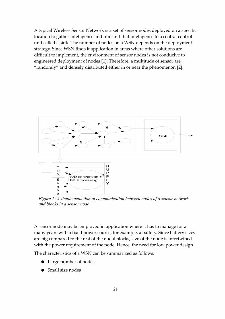
A simple type of common-mode feedback circuits (CMFB) was used. M1 and M2
are in deep triode region. This is achieved by selecting long transistors.
58
Figure 23: CMFB operation
Vcm
Vdesired Ibias
Vcm is used to bias the lower NMOS transistors of the amplifier.
2∣V in+−V dd−V th∣≫∣V cm−V dd∣, the same is true for M 2
V cm=V in++V in-
2. ............................................ (19)
3.2.4 ComparatorThe circuit used for the comparator is shown in figure 25. Of the two inputs of the comparator, one of them is from the baseband amplifier output whereas the other is a filtered version of the first. In order to keep the duty-cycle close to 50%, a single output of the amplifier is passed through a simple RC circuit and fed to the second input of comparator.
59
Figure 24: Common-Mode Feedback Circuit
In+ In-
Vcm
M1 M2
Deep triode operation
This current is copied by the mirror
transistorsIcmfb_bias

Due to the type of CMFB used in the baseband amplifier, the swings at its two outputs are not the same. The maximum swing that can be obtained from the first is input small and fixed where the other one has a swing that changes with input. Hence, the one with highest swing is passed through the circuit of figure 27 and fed to In- of figure 25. The value of the biasing currents I_sink and I_source is the same.
Figure 26 is the inverter circuit at the output of figure 25. It is used for further adjusting the swing and to create signals that are suitable to the subsequent digital baseband.
60
Figure 25: Comparator circuit, biasing not shown
outIn+ In-
I_sink
I_sourceR

Figure 27 shows the low pass filter through the output of the baseband amplifier passes before it is fed to the other input, In-, of the comparator.
Since big resistor and big capacitor are used, the output of the RC filter is a slower and smoother than the first. As long as there is enough voltage difference in the transition edges, the inverter connected to the output of the comparator outputs digital bits.
61
Figure 26: Inverter at the output of comparator
Vcomp Digital output
Wake-up codes are sent for
decoding to the digital baseband
Output of the comparator
Figure 27: RC filter at the other input of the comparator
Baseband Amplifier Out
Comparator Input
Big C
Big RLPF

The discussion of the circuits used for the wake-up receiver ends here. We have the mechanism by which the receiver architecture operates. The circuits that are used to receive, amplify, downconvert are discussed. In the next chapter, we will see the simulation results of these discussed circuits.
62

63

Chapter 4
Wake-up Receiver Simulation Results
In this chapter, simulation results of the actual circuits are presented. To minimize power consumption, small width of transistors were used. When possible longer transistors were selected. Transistors lengths which are two to five times the minimum length (120nm for this process) are advisable for analog design [18]. Most transistors are operated in the moderate inversion region.
Simple mirror circuits were used for biasing in the RF amplifier, envelope detector and baseband amplifier. The circuits were designed initially for 1V power supply. However, as there was only 1.2V LDO, some of the circuits were optimized for the new supply voltage. A 5µA current reference has been copied for biasing most of the circuits.
64

An external input matching circuit has been used. Except a DC blocking input capacitance, which is on-chip, all the other components are off-chip. The matching circuit is a capacitor transformer similar to one used here [9].
In addition to the actual wake-up receiver circuit, a test buffer is included to minimize the number of pins in the final chip. Inputs to the comparator and output from the baseband amplifier and the receiver can be selected for measurement.
In the testbench, the wake-up codes are modulated on to an RF carrier using a multiplier. A screenshot of the testbench used is below:
4.1 RF AmplifierThe common source transistor of the amplifier is a wide transistor with multiple fingers. Shorter lengths increase the power consumption; however, good gm/Id
ratio of 19 is obtained at 2*Lmin. The cascode transistor is optimized for 2.4GHz operation of the active inductor and a good gain for the amplifier.
The transistors in the active inductor are designed with minimum lengths. M_L1
has gm of 183µS and M_L2 is designed for a gm of 20µS and M_L3 passes a drain
65
Figure 28: WuRx testbench

current of around 3.5% of the total current flow in M_L1. Parasitics were used for simulation in the output node and at the gate of M_L1.
A biasing voltage at the gate of M1 keep the transistor in moderate inversion. To lessen the noise contribution of the resistor feeding the bias to the transistor, high value (10kΩ) poly resistor is used.
The input matching circuit is a capacitor transformer and is shown below:
The gain of the amplifier when simulated with the envelope detector connected to its output, the output and input waveforms and the input match, S11, are in the next figures.
66
Figure 29: Input matching network
C1
C2
CvarL1
RF input To RF amplifier

The input matching network is external. For measurement purposes, the capacitors can be varied for better match.
As can be seen from the above figure, the gain of the RF amplifier is wide-band. In other words, the selectivity of the RF amplifier is poor. Therefore, the input
67
Figure 30: input match, S11 - Schematic Level
Figure 31: Gain of RF amplifier - Schematic Level
matching network is expected to have a narrow gain curve. As node address is part of the packet sent in nodal communication, the effect of false wake-up is reduced. Therefore, problems of a wideband RF amplifier may not be severe.
68

The simulated schematic level total power consumption of the RF amplifier is 41µA at 1.2V supply. The gain of the amplifier is highly dependent on the active
69
Figure 33: Voltage gain of the RF amplifier – Layout Level
Figure 32: RF amplifier gain – Layout Level

inductor resonance frequency. As parasitics lower the resonance frequency, the gain lowers too. A voltage gain of 9.5dB is found after layout and a gain of around 12dB in schematic. Originally the circuit was designed for a 1V supply and a similar voltage gain was obtained at a power consumption of 36µA.
4.2 Envelope DetectorTransistor M1 is in weak inversion. Wide transistors choice in the envelope detector are easier to operate in weak inversion as they have higher gm value and higher source potential. Higher gm value gives wide bandwidth. Nonetheless, wide transistors also have an added penalty of gate capacitance which could offset the resonance frequency of the active inductor in the RF amplifier. Thus, it is a trade-off. As the gain of the envelope detector decreases with input level, it is reasonable to choose a transistor width so as to obtain a good gain at the amplifier even it lowers the conversion gain of the detector by some amount.
Minimum transistor length is used to lower gate capacitance and a biasing current of 1µA which gives a power consumption of 1.2µW. As it is variation of biasing voltage in one of the gates of the baseband amplifier could affect the stability of the opamp, two similar detectors are used for biasing the op-amp inputs.
The main transistor has a gm value of 24µS and an output capacitance of 1pF is connected at the output. Using the formula derived in the previous chapter, this gives a bandwidth of 3.8MHz. This is enough for data rates up to 100kHz.
The output waveform of the envelope detector is in the next figure.
70

4.3 Baseband AmplifierThe operational amplifier is mainly optimized for gain, bandwidth and phase margin. A 40fF MIM-cap miller capacitance and a 10kΩ poly resistor are used in the feedback circuit. The output common-mode voltage is kept higher to suit the biasing of the subsequent comparator. A current consumption of 7µA at 1.2V supply is obtained. The gain, phase and outputs waveforms of the baseband amplifier are shown below:
71
Figure 34: ED output at schematic level for 450µV input

4.4 ComparatorOnly one of the outputs of the baseband amplifier drives one of the inputs of the comparator. The swing from the negative output node of the amplifier is affected by the voltage headroom in the common-mode feedback circuit, hence, the other input is used to drive the comparator. The comparator detects as low as 7mV difference between the input levels. It has a current consumption of not more than 5µA at 1.2V supply. Output waveforms from the comparator and that of the inverter are shown below:
72
Figure 35: Phase and gain curves of the baseband amplifier

The above figure shows the operation of the comparator. One of the inputs of the baseband amplifier and its RC-filtered version are the input to the comparator. The output is digital whose duty ratio is fairly constant for different input values.
73
Figure 36: Comparator Operation

4.5 Summary
The wake-up receiver power is dominated by the RF amplifier. The pie-chart in figure 37 shows the power ratio at schemtic level. The RF amplifier consumes a little more than 60% of the total power budget of the WuRx. In account of the reference current source (5µA) used, the biasing circuit takes the next bigger slice of power. It is clear how much the total power consumption can be improved with a low reference. The baseband amplifier is the third highest power consuming block. The reason being it has an additional CMFB circuit.
74

The operation of the wake-up receiver at minimum input signal can be seen in the following graphs.
75
Figure 37: The ratio of the total power budget consumed by each WuRx block
RF AmpEDBB AmpCompBiasing

Because Transient analysis takes long time for simulating the whole wake-up receiver, it is only used for comparing the results with that found using Envelope Analysis. The graphs are from an Envelope analysis. The input is an OOK modulated RF signal. The second graph is at the output of the RF amplifier. The third is at ED output and the inputs and output of the comparator are drawn last. The digital output is the output of the WuRx and this is fed to the digital baseband for decoding.
Figure 39 is a screenshot of the wake-up receiver layout.
76
Figure 38: Operation of WuRx at minimum input signal using Envelope analysis

A modified version, but not taped out, can be found in the next figure. It is the same receiver except the testbuffer is removed. There is not a significant difference in performance.
77
Figure 39: A screenshot of the wake-up receiver layout with its test buffer

78
Figure 40: A modified wake-up receiver layout

79

Chapter 5
Conclusion and Future Work
Although the results obtained for the wake-up receiver are only simulated and not measured, we can still compare its performance to some of the recent works in the area. As there will be an improved implementation of the wake-up receiver in the future, these comparisons will put the strengths and weaknesses of the wake-up receiver in terms of architecture, circuit topologies and systems level choices in perspective.
5.1 ComparisonWhile wake-up receiver is a recently proposed method, there has been many publications in the last 4 to 5 years. Most of these works have investigated different architectures for improving the sensitivity and power consumption of the receiver. As far as my literature review, the uncertain-IF receiver and the tuned-RF receiver with double-sampling discussed in the chapter two have the
80

best power and sensitivity performance for a wake-up receiver. There are others which have an improved sensitivity and power performance, however, these blend the two nodal communication methods – duty-cycling and using a wake-up receiver. They do this by further duty-cycling the wake-up receiver.
Four receivers are included in the comparison as shown in the following table.
This work is closely similar to the first one in the table. The above work uses MEMS for input matching. This increases the cost of the receiver. Another difference is in the baseband implementation. The above work uses a 20mW ADC. This has increased the total power significantly. The envelope detector used in that work is biased using an offset-calibration DAC. The front-end amplifier uses bulk biasing for lowering threshold voltages of the cascode transistors and those in the active inductor.
The second work, also from Berkeley Wireless Research Center (BWRC), does not have an ADC. It has an envelope detector at its output stage. Although a 20pF capacitor is used at the output of the ED, still, the output will not be digital and hence the wake-up receiver does not account for the additional power
81
Table 2: The wake-up receiver compared with other wake-up receivers
Works Powerin µW
Sens.in dBm
Data Ratein kb/s
Freq.in GHz
CMOSTech.
Volin V
[21] 65 -47 100 1.9 90nm 0.5[8] 52 -72 100 1.9 90nm 0.5[9] 51 -64 10 2.4 90nm 0.5[10] 53 -75 100 2.4 0.18m
m1.8
This work
69µA @1.2V
-52 100 2.4 130nm 1.2

consumption that could be incurred for converting the output of the ED to digital.
The third work uses two external inductor in its front-end amplifier – for matching and tuning. If the system is to be integrated, The wake-up receiver may not have the same performance – -64dBm sensitivity, 51µW power at 100kb/s.
The fourth work is a duty-cycled WuRx. It has a much lower power consumption. The future work of this thesis project is to implement the wake-up receiver using a duty-cycling mechanism.
With respect to the two critical requirements, power and sensitivity, the wake-up receiver results are only satisfactory. The design work is only “experimental”, nevertheless, minor changes such as a 1V LDO and a 1µA reference current could improve the wake-up receiver power consumption to less than 50µW. For example, a similar gain and power consumption is obtained for the RF amplifier at its previous supply voltage – 1V. Due to time shortage, the baseband amplifier is not optimized for lower power. The biasing and CMFB of this amplifier can be modified to further lower the consumption by at least 3µA.
5.1 Future WorkWith the designed wake-up receiver, the range of communication is limited. In WSN, this increases the number of nodes and the total cost of implementation. Assuming a 0dBm transmitter for wake-up codes, the loss at different distances from one node can be calculated by using the free space path loss formula [19]:
LFS (dB)=32.4+20log r+20log f , ........................................... (20)Where r is distance in kilometeres, and f is frequency in MHz.
At 4meters, the signal has a power of -52dBm. This means the wake-up receiver can only work up to this distance. As this affects the total cost of implementation, the practicality of the wake-up receiver for nodal communication is less convincing. With power-aware duty-cycling, the main transceiver is less costly than wake-up receiver scheme employing a low sensitivity WuRx for nodal communication. The reason being the main transceiver has higher sensitivity and can cover large area despite problems of longer latency and increased power dissipation. To put this in perspective, a work comparing wake-up receiver scheme with duty-cycled nodal communication is referred [20]. In this paper, the effect of wake-up receiver sensitivity on the total cost of a WSN is analyzed. It is concluded that wake-up receiver scheme is feasible when its sensitivity is at least -80dBm. The number of nodes used in the analysis is based on a mathematically calculated figure and does not take into consideration the deployment of higher
82

number of sensor nodes to mitigate effects of failure, nonetheless, the conclusion strengths that a sensitivity of -52dBm is low for a practical WuRx.
To overcome this problem, a future work targets on increasing the sensitivity by employing duty-cycling. As the whole wake-up receiver will be turned-on for a small percentage of a period, the total power consumption is multiplied by the duty-cycle. For example, a 20% duty-cycled wake-up receiver designed at 100µW will actually have a power consumption of only 20µW. The method enables the use of higher power consumption RF amplifier in the front-end to obtain a higher gain. Two RF amplifiers in cascade before the envelope detector is also an effective approach.
83

84

Bibliography[1] W. Dargie, C. Poellabauer, Fundamentals of Wireless Sensor Networks Theory
and Practice, John Wiley & Sons Ltd., 2010.
[2] I. F. Akyildiz, W. Su, Y. Sankarasubramaniam and E. Cayirci, “Wireless Sensor
Networks: A Survey”, Computer Networks (Elsevier) Journal, vol. 38, no. 4, pp.
393 – 422, March 2002.
[3] M. Reyer, S. Hurlebaus, J. Mander, O. E. Ozbulut, “Design of a wirelss sensor
network for Structural Health Monitoring of bridges,” in Fifth International
Conference on Sensing Technology, 2011, pp. 515-520.
[4] B. Zhao and H. Yang (2010). Design of Radio-Frequency Transceivers for
Wireless Sensor Networks, Wireless Sensor Networks: Application-Centric
Design, , , ISBN: 978-953-307-321-7, InTech, Available from:
http://www.intechopen.com/books/wireless-sensor-networks-application-centric-
design/design-of-radio-frequency-transceivers-for-wireless-sensor-networks
[5] E.-Y. Lin, J. Rabaey, and A. Wolisz, "Power-efficient rendez-vous schemes for
dense wireless sensor networks," in IEEE International Conference on
Communications, Vol. 7, no. , pp. 3769-3776, June 2004.
[6] M. Olofsson, Introduction to Digital Communication, Linköping: Linköping
University, August 2010.
85

[7] M. S. Durante, S. Mahlknecht, "An ultra low power Wakeup Receiver for
Wireless Sensor Networks," in Proceedings of the 2009 Third International
Conference on Sensor Technologies and Applications, vol. 00, 2009, pp. 167-170.
[8] N. M. Pletcher, S. Gambini and J. Rabaey, "A 2GHz 52 microWatt wake-up
receiver with -72dBm sensitivity using uncertain-IF architecture," in IEEE Journal
of Solid State Circuits Conference, February 2008, San Francisco, CA.
[9] W. Huang, S. Rampu, X. Wang, G. Dolmans and H. d. Groot, "A
2.4GHz/915MHz 51 microWatt Wake-Up Receiver with Offset and Noise
Suppression," in IEEE International Solid State Circuits Conference, 2010, San
Franscisco, CA.
[10] X. Yu, Jeong-Seon Lee, C. Shu, and Sang-Gug Lee, "A 53mW Super-
Regenerative Receiver for 2.4GHz Wake-up Application," in IEEE Asia-Pacific
Microwave Conference, 2008.
[11] N. Pletcher, J. M. Rabaey, "Ultra-Low Power Wake-Up Receivers for Wireless
Sensor Networks," Ph.D. Dissertation, University of California, Berkeley, 2008.
[12] E. Nilsson, C. Svensson, "Envelope Detector Sensitivity and Blocking
Characteristics," in 20th European Conference on Circuit Theory and Design,
August 2011, pp. 773 – 776.
[13] S. Gambini, N. Pletcher, and J. M. Rabaey, "Sensitivity Analysis for AM
detectors," in EECS Department, University of California, Berkeley, Tech. Rep.
UCB/EECS-2008-31, April 2008. Available from:
http://www.eecs.berkeley.edu/Pubs/TechRpts/2008/EECS-2008-31.html
86
[14] R. G. Meyer, “Low-Power Monolithic RF Peak Detector Analysis,” in IEEE
Journal of Solid State Circuits, vol. 30, no. 1, pp. 65-67, January 1995.
[15] B. Razavi, Design of Analog CMOS Integrated Circuits, New York: McGraw-
Hill , 2001.
[16] D. J. Comer and D. T. Comer,, "Using the weak inversion region to
optimizeinput stage design of CMOS op amps," in Circuits and Systems II:
Express Briefs, Vol. 51, no. 1, pp. 8-14, 2004.
[17] Y. Wu, M. Ismail, and H. Olsson, "A nover CMOS fully differential
inductorless RF bandpass Filter," in Proceedings of the IEEE International
Symposium on Circuits and Systems, Vol. 4, May 2000, pp. 149-152.
[18] W. M.C. Sansen, Analog Design Essentials, Dordrecht, The Netherlands:
Springer, 2006.
[19] L. Ahlin, J. Zander, B. Slimane, Principles of Wireless Communications,
Studentlitteratur, 2006.
[20] R. Su, T. W., K. S. J. Pister, “Comparison between Preamble Sampling and
Wake-Up Receivers in Wireless Sensor Networks,” in Proceedings of the IEEE
Global Telecommunications Conference, 2010.
[21] N. Pletcher, S. Gambini and J. M. Rabaey, “A 65µW, 1.9GHz RF to digital
baseband wakeup receiver for wireless sensor nodes,” in IEEE Custom Integrated
Circuits Conference, pp. 539 – 542, September 2007.
87

[22] B. Razavi, RF Microelectronics, 2nd ed. Prentice Hall, 2011.
88