Embed Size (px)
Citation preview

EEDG 6306
ASIC DESIGN OF
MINI-STEREO DIGITAL AUDIO PROCESSOR
UNDER IBM 130NM TECHNOLOGY
FINAL PROJECT REPORT
ILANGO JEYASUBRAMANIAN - ixj150230
SABARISH SEKAR – sxs154930

INDEX
1 INTRODUCTION
2 HARDWARE IMPLEMENTATION
3 BLOCK DIAGRAM
4 PORT DESCRIPTION
5 DATA FORMATS
6 FINITE STATE MACHINE AND
OPERATING MODES OF MSDAP
7 PIN CONFIGURATION
9 COMPUTATION
10 SIMULATION WAVEFORM
1.INTRODUCTION:
1.1 What is ASIC design?
An application-specific integrated circuit (ASIC) is an integrated circuit (IC) customized for a
particular use, rather than intended for general-purpose use. For example, a chip designed to run
in a digital voice recorder or a high-efficiency Bitcoin miner is an ASIC. Application-specific
standard products (ASSPs) are intermediate between ASICs and industry standard integrated
circuits like the 7400 or the 4000 series.
As feature sizes have shrunk and design tools improved over the years, the maximum complexity
(and hence functionality) possible in an ASIC has grown from 5,000 gates to over 100 million.
Modern ASICs often include entire microprocessors, memory blocks including ROM, RAM,
EEPROM, flash memory and other large building blocks. Such an ASIC is often termed a SoC
(system-on-chip). Designers of digital ASICs often use a hardware description language (HDL),
such as Verilog or VHDL, to describe the functionality of ASICs.
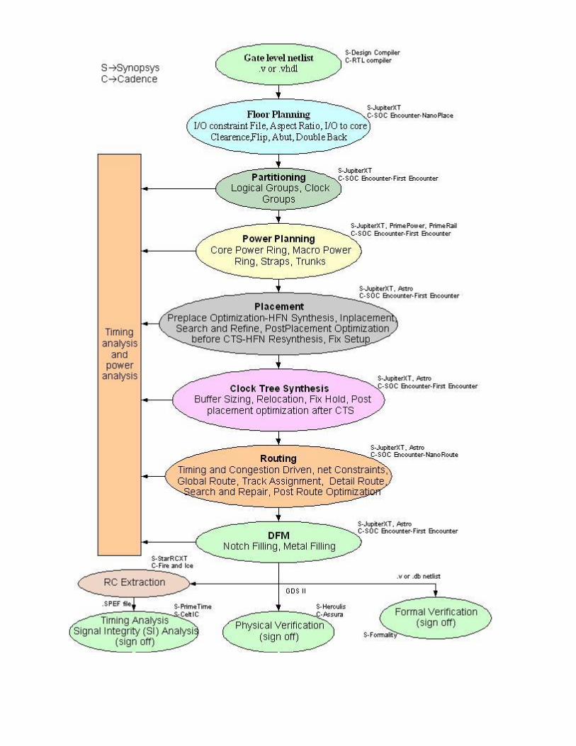
The main steps in the ASIC physical design flow are:
Design Netlist (after synthesis)
Floorplanning
Partitioning
Placement
Clock-tree Synthesis (CTS)
Routing
Physical Verification
GDS II Generation
These steps are just the basics. There are detailed PD flows that are used depending on the Tools
used and the methodology/technology. Some of the tools/software used in the back-end design
are :
Cadence (Cadence Encounter RTL Compiler, Encounter Digital Implementation, Cadence
Voltus IC Power Integrity Solution, Cadence Tempus Timing Signoff Solution)
Synopsys (Design Compiler, IC Compiler)
Magma (BlastFusion, etc.)
Mentor Graphics (Olympus SoC, IC-Station, Calibre)
A more detailed Physical Design Flow is shown below. Here you can see the exact steps and the
tools used in each step outlined.

1.2 What is Physical Design?
Physical design steps
Floorplanning
The first step in the physical design flow is Floorplanning. Floorplanning is the process of
identifying structures that should be placed close together, and allocating space for them in such a
manner as to meet the sometimes conflicting goals of available space (cost of the chip), required
performance, and the desire to have everything close to everything else.
Based on the area of the design and the hierarchy, a suitable floorplan is decided upon.
Floorplanning takes into account the macros used in the design, memory, other IP cores and their
placement needs, the routing possibilities and also the area of the entire design. Floorplanning also
decides the IO structure, aspect ratio of the design. A bad floorplan will lead to waste-age of die
area and routing congestion.
In many design methodologies, Area and Speed are considered to be things that should be traded
off against each other. The reason this is so is probably because there are limited routing resources,
and the more routing resources that are used, the slower the design will operate. Optimizing for
minimum area allows the design to use fewer resources, but also allows the sections of the design
to be closer together. This leads to shorter interconnect distances, less routing resources to be used,
faster end-to-end signal paths, and even faster and more consistent place and route times. Done
correctly, there are no negatives to floorplanning.
As a general rule, data-path sections benefit most from floorplanning, and random logic, state
machines, and other non-structured logic can safely be left to the placer section of the place and
route software.
Data paths are typically the areas of your design where multiple bits are processed in parallel with
each bit being modified the same way with maybe some influence from adjacent bits. Example
structures that make up data paths are Adders, Subtractors, Counters, Registers, and Muxes.
Partitioning
Partitioning is a process of dividing the chip into small blocks. This is done mainly to separate
different functional blocks and also to make placement and routing easier. Partitioning can be done
in the RTL design phase when the design engineer partitions the entire design into sub-blocks and
then proceeds to design each module. These modules are linked together in the main module called
the TOP LEVEL module. This kind of partitioning is commonly referred to as Logical Partitioning.
Placement
Before the start of placement optimization all Wire Load Models (WLM) are removed. Placement
uses RC values from Virtual Route (VR) to calculate timing. VR is the shortest Manhattan distance
between two pins. VR RCs are more accurate than WLM RCs.
Placement is performed in four optimization phases:
Pre-placement optimization
In placement optimization
Post Placement Optimization (PPO) before clock tree synthesis (CTS)
PPO after CTS.
Pre-placement Optimization optimizes the netlist before placement, HFNs are collapsed. It can
also downsize the cells.In-placement optimization re-optimizes the logic based on VR. This can
perform cell sizing, cell moving, cell bypassing, net splitting, gate duplication, buffer insertion,
area recovery. Optimization performs iteration of setup fixing, incremental timing and congestion
driven placement.Post placement optimization before CTS performs netlist optimization with ideal
clocks. It can fix setup, hold, max trans/cap violations. It can do placement optimization based on
global routing. It re does HFN synthesis.Post placement optimization after CTS optimizes timing
with propagated clock. It tries to preserve clock skew.
Clock tree synthesis
Ideal clock before CTS
The goal of clock tree synthesis (CTS) is to minimize skew and insertion delay. Clock is not
propagated before CTS as shown in the picture. After CTS hold slack should improve. Clock tree
begins at .sdc defined clock source and ends at stop pins of flop. There are two types of stop pins
known as ignore pins and sync pins. ‘Don’t touch’ circuits and pins in front end (logic synthesis)
are treated as ‘ignore’ circuits or pins at back end (physical synthesis). ‘Ignore’ pins are ignored
for timing analysis. If clock is divided then separate skew analysis is necessary.
Global skew achieves zero skew between two synchronous pins without considering logic
relationship.
Local skew achieves zero skew between two synchronous pins while considering logic
relationship.
If clock is skewed intentionally to improve setup slack then it is known as useful skew.
Rigidity is the term coined in Astro to indicate the relaxation of constraints. Higher the rigidity
tighter is the constraints.
Clock After CTS
In clock tree optimization (CTO) clock can be shielded so that noise is not coupled to other signals.
But shielding increases area by 12 to 15%. Since the clock signal is global in nature the same metal
layer used for power routing is used for clock also. CTO is achieved by buffer sizing, gate sizing,
buffer relocation, level adjustment and HFN synthesis. We try to improve setup slack in pre-
placement, in placement and post placement optimization before CTS stages while neglecting hold
slack. In post placement optimization after CTS hold slack is improved. As a result of CTS lot of
buffers are added. Generally for 100k gates around 650 buffers are added.
Routing
There are two types of routing in the physical design process, global routing and detailed routing.
Global routing allocates routing resources that are used for connections. It also does track
assignment for a particular net.
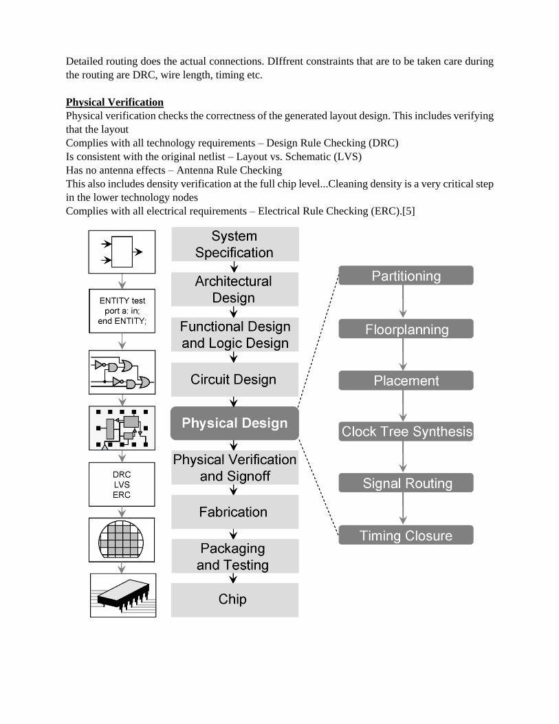
Detailed routing does the actual connections. DIffrent constraints that are to be taken care during
the routing are DRC, wire length, timing etc.
Physical Verification
Physical verification checks the correctness of the generated layout design. This includes verifying
that the layout
Complies with all technology requirements – Design Rule Checking (DRC)
Is consistent with the original netlist – Layout vs. Schematic (LVS)
Has no antenna effects – Antenna Rule Checking
This also includes density verification at the full chip level...Cleaning density is a very critical step
in the lower technology nodes
Complies with all electrical requirements – Electrical Rule Checking (ERC).[5]
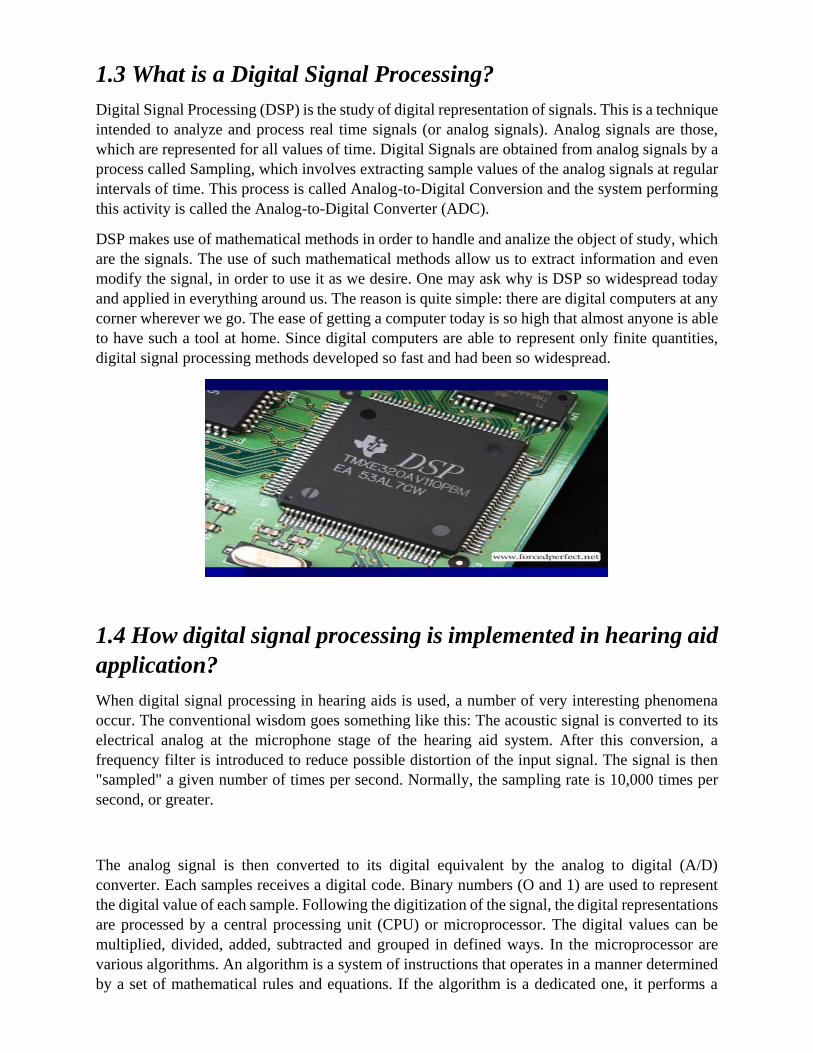
1.3 What is a Digital Signal Processing?
Digital Signal Processing (DSP) is the study of digital representation of signals. This is a technique
intended to analyze and process real time signals (or analog signals). Analog signals are those,
which are represented for all values of time. Digital Signals are obtained from analog signals by a
process called Sampling, which involves extracting sample values of the analog signals at regular
intervals of time. This process is called Analog-to-Digital Conversion and the system performing
this activity is called the Analog-to-Digital Converter (ADC).
DSP makes use of mathematical methods in order to handle and analize the object of study, which
are the signals. The use of such mathematical methods allow us to extract information and even
modify the signal, in order to use it as we desire. One may ask why is DSP so widespread today
and applied in everything around us. The reason is quite simple: there are digital computers at any
corner wherever we go. The ease of getting a computer today is so high that almost anyone is able
to have such a tool at home. Since digital computers are able to represent only finite quantities,
digital signal processing methods developed so fast and had been so widespread.
1.4 How digital signal processing is implemented in hearing aid
application?
When digital signal processing in hearing aids is used, a number of very interesting phenomena
occur. The conventional wisdom goes something like this: The acoustic signal is converted to its
electrical analog at the microphone stage of the hearing aid system. After this conversion, a
frequency filter is introduced to reduce possible distortion of the input signal. The signal is then
"sampled" a given number of times per second. Normally, the sampling rate is 10,000 times per
second, or greater.
The analog signal is then converted to its digital equivalent by the analog to digital (A/D)
converter. Each samples receives a digital code. Binary numbers (O and 1) are used to represent
the digital value of each sample. Following the digitization of the signal, the digital representations
are processed by a central processing unit (CPU) or microprocessor. The digital values can be
multiplied, divided, added, subtracted and grouped in defined ways. In the microprocessor are
various algorithms. An algorithm is a system of instructions that operates in a manner determined
by a set of mathematical rules and equations. If the algorithm is a dedicated one, it performs a
specific task relative to the processing of the input signal. For example, one algorithm may control
the frequency response of the instrument, another may control loudness growth, a third may
function to enhance the speech signal in a background of noise, etc. After the microprocessor has
performed its tasks, the digitized signal must be converted back to its analog equivalent. This is
accomplished at the digital to analog (D/A) conversion stage. When the digitized signal is
converted to its analog stage, it is frequency filtered again, to prevent signal distortion. It is then
amplified in the conventional manner and submitted to the receiver (speaker) of the hearing aid.
(Note: For some of the more recent DSP systems, the D/A conversion does not require a separate
circuit. Rather, it uses the hearing aid receiver to accomplish digital to analog conversion. This
process is referred to as a Direct Digital Drive.)
The obvious advantage of digital signal processing is that there are unlimited ways in which the
signal can be manipulated. The number of parameters that can be utilized, and that can be utilized
at the same instant in time, are significantly greater than those found in conventional analog
systems. As such, the ability to manipulate the signal to more closely approximate the acoustic
needs of the patient is greatly enhanced.
2.HARDWARE IMPLEMENTATION
The main function of this MSDAP processor is a two-channel, 512 order, finite impulse
response (FIR) digital filter. It receives 16-bit voice data (sampled at 768 kHz) and computes the
FIR result at the speed of 94.33MHz. The chip computes the following linear convolution:
𝒚(𝒏) = ∑ 𝒉(𝒌) × 𝒙(𝒏 − 𝒌)
𝑵
𝒌=𝟎
where x(n) and y(n) are input and output audio sequences, and h(k) are filter coefficients with
the filter order 512.
However, in order to reduce the hardware complexity, the multiplications are avoided
by replacing multiplications with shift operations. This is done by taking power-of-two digits as
filter coefficients for computation.
ℎ(𝑘) × 𝑥(𝑛 − 𝑘) = 2−3𝑥(𝑛 − 𝑘) − 2−7𝑥(𝑛 − 𝑘) + 2−16𝑥(𝑛 − 𝑘)
The Finite state machine designed represents the following system block diagram with one MSDAP
block and a controller communicated in an asynchronous manner with the following input and output
ports.
PORT SPECIFICATION:
INPUT SIGNALS : Sclk, Dclk, Start, Reset_n, InputL, InputR, Frame
OUTPUT SIGNALS: InReady, OutReady, OutputL, OutputR
CLOCKS : Sclk, Dclk
FREQUENCY OF DCLK: 768KHz
FREQUENCY OF SCLK : 94.33Hz
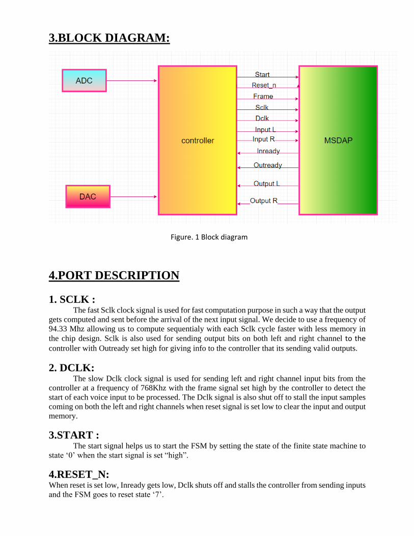
3.BLOCK DIAGRAM:
Figure. 1 Block diagram
4.PORT DESCRIPTION
1. SCLK : The fast Sclk clock signal is used for fast computation purpose in such a way that the output
gets computed and sent before the arrival of the next input signal. We decide to use a frequency of
94.33 Mhz allowing us to compute sequentialy with each Sclk cycle faster with less memory in
the chip design. Sclk is also used for sending output bits on both left and right channel to the controller with Outready set high for giving info to the controller that its sending valid outputs.
2. DCLK: The slow Dclk clock signal is used for sending left and right channel input bits from the
controller at a frequency of 768Khz with the frame signal set high by the controller to detect the
start of each voice input to be processed. The Dclk signal is also shut off to stall the input samples
coming on both the left and right channels when reset signal is set low to clear the input and output
memory.
3.START : The start signal helps us to start the FSM by setting the state of the finite state machine to
state ‘0’ when the start signal is set “high”.
4.RESET_N: When reset is set low, Inready gets low, Dclk shuts off and stalls the controller from sending inputs
and the FSM goes to reset state ‘7’.
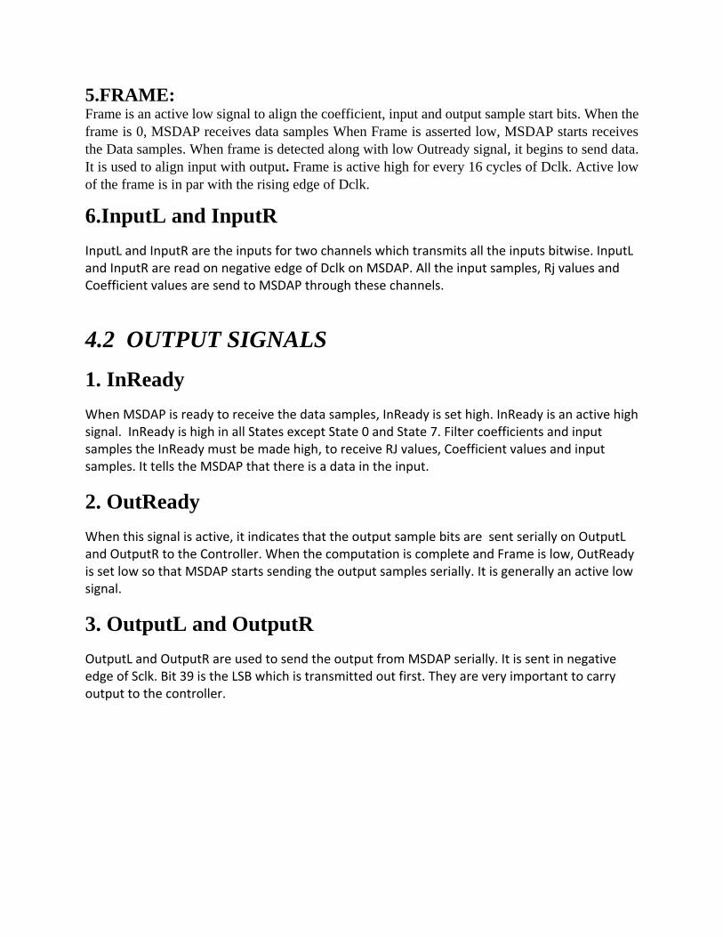
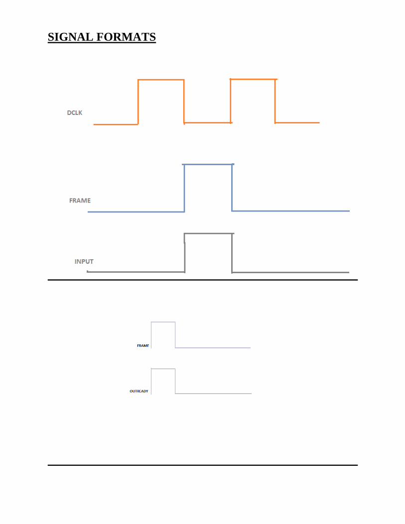
5.FRAME: Frame is an active low signal to align the coefficient, input and output sample start bits. When the
frame is 0, MSDAP receives data samples When Frame is asserted low, MSDAP starts receives
the Data samples. When frame is detected along with low Outready signal, it begins to send data.
It is used to align input with output. Frame is active high for every 16 cycles of Dclk. Active low
of the frame is in par with the rising edge of Dclk.
6.InputL and InputR
InputL and InputR are the inputs for two channels which transmits all the inputs bitwise. InputL and InputR are read on negative edge of Dclk on MSDAP. All the input samples, Rj values and Coefficient values are send to MSDAP through these channels.
4.2 OUTPUT SIGNALS
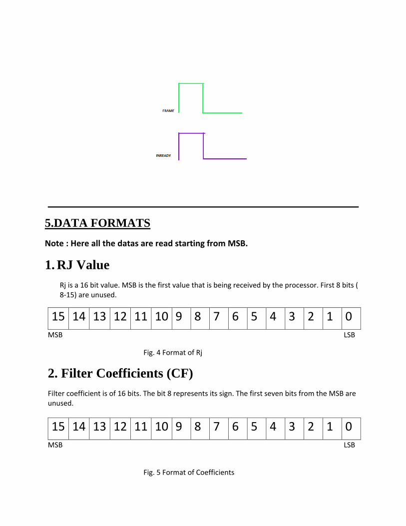
1. InReady
When MSDAP is ready to receive the data samples, InReady is set high. InReady is an active high signal. InReady is high in all States except State 0 and State 7. Filter coefficients and input samples the InReady must be made high, to receive RJ values, Coefficient values and input samples. It tells the MSDAP that there is a data in the input.
2. OutReady
When this signal is active, it indicates that the output sample bits are sent serially on OutputL and OutputR to the Controller. When the computation is complete and Frame is low, OutReady is set low so that MSDAP starts sending the output samples serially. It is generally an active low signal.
3. OutputL and OutputR
OutputL and OutputR are used to send the output from MSDAP serially. It is sent in negative edge of Sclk. Bit 39 is the LSB which is transmitted out first. They are very important to carry output to the controller.
SIGNAL FORMATS
5.DATA FORMATS
Note : Here all the datas are read starting from MSB.
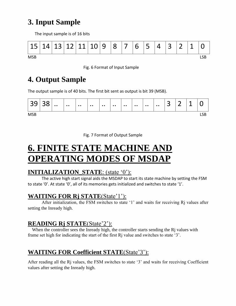
1. RJ Value
Rj is a 16 bit value. MSB is the first value that is being received by the processor. First 8 bits ( 8-15) are unused.
15 14 13 12 11 10 9 8 7 6 5 4 3 2 1 0
MSB LSB
Fig. 4 Format of Rj
2. Filter Coefficients (CF)
Filter coefficient is of 16 bits. The bit 8 represents its sign. The first seven bits from the MSB are unused.
15 14 13 12 11 10 9 8 7 6 5 4 3 2 1 0
MSB LSB
Fig. 5 Format of Coefficients
3. Input Sample
The input sample is of 16 bits
15 14 13 12 11 10 9 8 7 6 5 4 3 2 1 0
MSB LSB
Fig. 6 Format of Input Sample
4. Output Sample
The output sample is of 40 bits. The first bit sent as output is bit 39 (MSB).
39 38 .. .. .. .. .. .. .. .. .. .. 3 2 1 0
MSB LSB
Fig. 7 Format of Output Sample
6. FINITE STATE MACHINE AND
OPERATING MODES OF MSDAP
INITIALIZATION_STATE: (state ‘0’): The active high start signal aids the MSDAP to start its state machine by setting the FSM
to state ‘0’. At state ‘0’, all of its memories gets initialized and switches to state ‘1’.
WAITING FOR Rj STATE(State’1’): After initialization, the FSM switches to state ‘1’ and waits for receiving Rj values after
setting the Inready high.
READING Rj STATE(State’2’): When the controller sees the Inready high, the controller starts sending the Rj values with
frame set high for indicating the start of the first Rj value and switches to state ‘3’.
WAITING FOR Coefficient STATE(State’3’):
After reading all the Rj values, the FSM switches to state ‘3’ and waits for receiving Coefficient
values after setting the Inready high.

READING Coefficient STATE(State’4’): When the controller sees the Inready high, the controller starts sending the Coefficient values with
frame set high for indicating the start of the first Coefficient value and switches to state ‘5’.
WAITING FOR InputSTATE(State’5’): After reading all the Coefficient values, the FSM switches to state ‘5’ and waits for receiving
Coefficient values after setting the Inready high.
READING Input STATE and WORKING STATE(State’6’): When the controller sees the Inready high, the controller starts sending the Input values at both
left and right channels with frame set high for indicating the start of the first input value at both
the channels and starts reading the inputs at both the channels.
RESET STATE(State’7’): We can see that when reset is set low, Inready gets low, Dclk shuts off and stalls the controller
from sending inputs and the FSM goes to reset state ‘7’. At the reset state, all the input and output
memory gets cleared and stays in reset state until reset remains low. When reset gets high at reset
state ‘7’, the chip goes to state ‘5’ and waits for receiving input samples after setting Inready high.
When the controller sets Inready high, it starts sending the next input with the frame set high to
indicate the start of the next input. The MSDAP sees the frame set high and goes to working state
and starts reading the next inputs.
SLEEPING STATE(State ‘8’): For going to sleep state, if we are receiving 800 continuous16-bit zeros (i.e 12800 zero input bits)
at both the left and right channels in the working state, we will switch to sleep state ‘8’ and stall
computing the outputs.we also constantly receive inputs without storing the data. At the first non-
zero 16-bit input, we will store this data as the next input and switch to the working state ‘6’. This
is done by temporarily storing the data in the registers “tempL” and “tempR” for checking if we
are receiving a non-zero 16-bit input

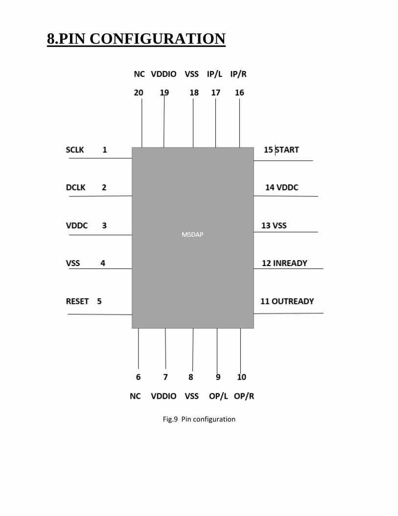
8.PIN CONFIGURATION
Fig.9 Pin configuration
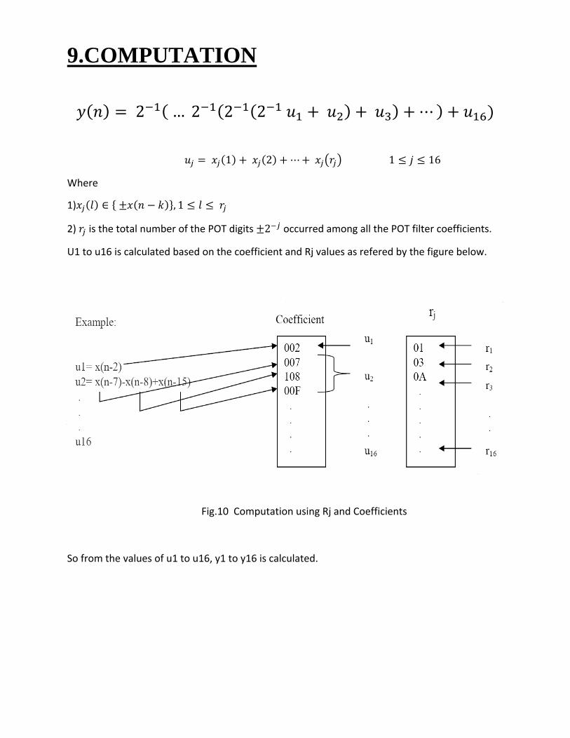
9.COMPUTATION
𝑦(𝑛) = 2−1( … 2−1(2−1(2−1 𝑢1 + 𝑢2) + 𝑢3) + ⋯ ) + 𝑢16)
𝑢𝑗 = 𝑥𝑗(1) + 𝑥𝑗(2) + ⋯ + 𝑥𝑗(𝑟𝑗) 1 ≤ 𝑗 ≤ 16
Where
1)𝑥𝑗(𝑙) ∈ { ±𝑥(𝑛 − 𝑘)}, 1 ≤ 𝑙 ≤ 𝑟𝑗
2) 𝑟𝑗 is the total number of the POT digits ±2−𝑗 occurred among all the POT filter coefficients.
U1 to u16 is calculated based on the coefficient and Rj values as refered by the figure below.
Fig.10 Computation using Rj and Coefficients
So from the values of u1 to u16, y1 to y16 is calculated.
• The input
format for the
C-program of
Exercise 3-1.
• This format is
also adopted
late in the
implementation
of the MSDAP
chip.

10.MSDAP ARCHITECTURE
The MSDAP consists of following blocks:
1) Serial to parallel control
2) Main Controller
3) ALU
4) RJ memory Left
5) RJ memory Right
6) COEFF memory Left
7) COEFF memory Right
8) DATA memory Left
9) DATA memory Right
10) Sign extension Left
11) Sign Extension Right
12) Adder Left
13) Adder Right
14) Shifter Left
15) Shifter Right
16) Parallel to Serial Control
17) Zero Detector
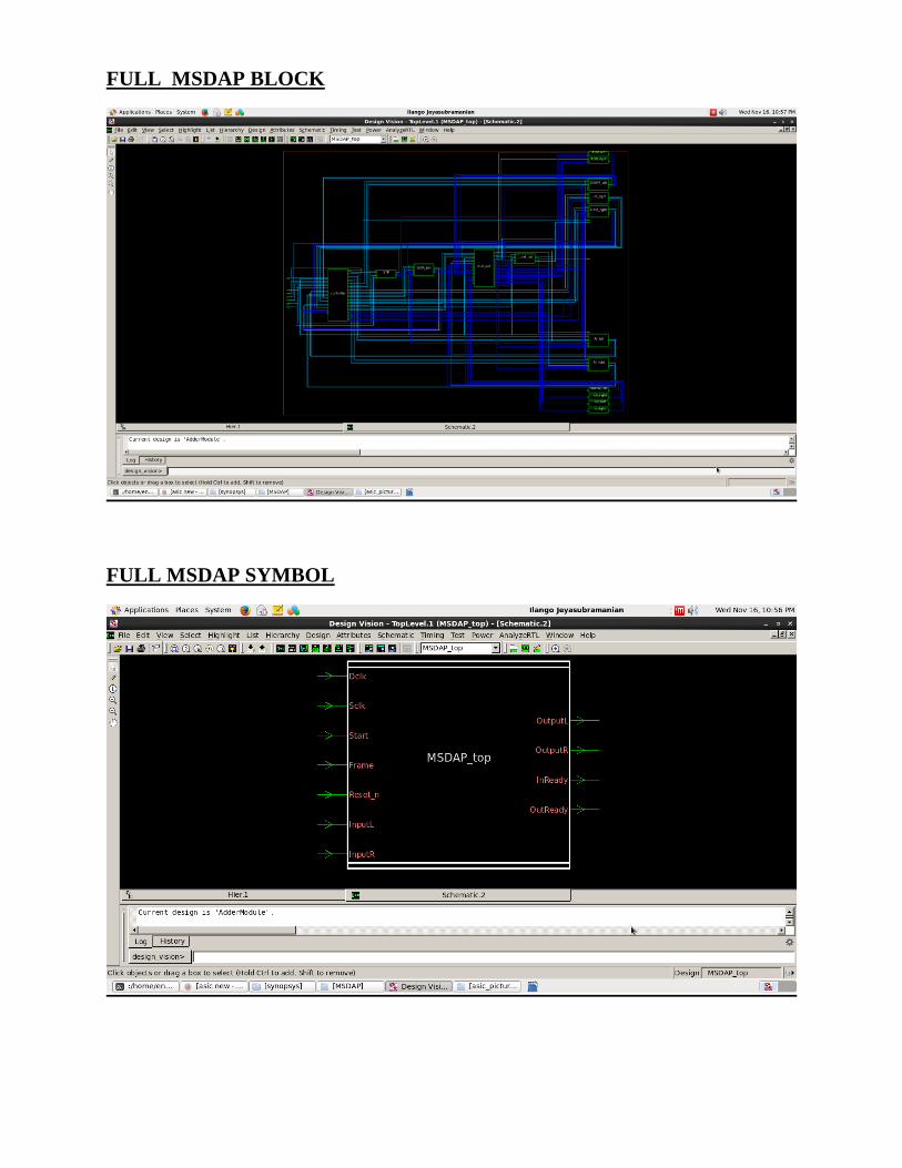
FULL MSDAP BLOCK
FULL MSDAP SYMBOL

SERIAL TO PARALLEL CONVERTER
Inputs (Input L and Input R) from the file is fed into this module which converts the serial input
into parallel. This works with reference with the Dclk. Serial to parallel module receives the data
when it encounters low STP_enable signal. STP_ready is made high after receiving 16 bits so as
to indicate controller as it is ready to get the next 16 bits.Clear signal is used to indicate that
MSDAP has started to clear all its registers, which is generally used in the State 0.
SIGNALS USED IN THIS MODULE
INPUT SIGNALS AND DATA
STP_enable : Enables the serial to parallel conversion module
Dclk : Data clock signal
InputL : Left channel serial input bits
InputR : Right channel serial input bits
OUTPUT SIGNALS AND DATA
Data_parallel_left : Converted parallel left data
Data_parallel_right : Converted parallel right data
STP_ready : Indicates that parallel conversion is done and the corresponding
parallel data is ready.
ALU BLOCK
The entire arithmetic and logical operations are performed inside this block. This works in
correspondence with Sclk and Frame.
SIGNALS USED IN THE MODULE
INPUT SIGNALS AND DATA
ALU_enable :Enables the ALU unit
ALU_start :Brings the ALU to the start of its own sub-state machine.
Sclk :High frequency system clock signal for faster computation.
Frame :Indicates the start of the new data MSB bit.
FROM RJ BLOCK
RJ_ready_left :Indicates that data from RJ_memory_left is sent for the corresponding
RJ_address_left
RJ_ready_right :Indicates that data from RJ_memory_right is sent for the corresponding
RJ_address_right
RJ_out_left :The data coming out from RJ_memory_left for the corresponding
RJ_read_address_left
RJ_out_right:The data coming out from RJ_memory_right for the corresponding
RJ_read_address_right
FROM COEFF BLOCK
COEFF_ready_left :Indicates that data from COEFF_memory_left is sent for the
corresponding COEFF_address_left
COEFF_ready_right :Indicates that data from COEFF_memory_right is sent for the
corresponding COEFF_address_right
COEFF_out_left :The data coming out from COEFF_memory_left for the corresponding
COEFF_read_address_left
COEFF_out_right :The data coming out from COEFF_memory_right for the corresponding
COEFF_read_address_right
FROM DATA BLOCK
DATA_read_ready_left : Indicates that data from DATA_memory_left is sent for the
corresponding DATA_address_left
DATA_read_ready_right : Indicates that data from DATA_memory_left is sent for the
corresponding DATA_address_left
DATA_out_left : The data coming out from DATA_memory_left for the
corresponding DATA_read_address_left
DATA_out_right : The data coming out from DATA_memory_right for the
corresponding DATA_read_address_right
FROM ADDER BLOCK
Add_output_left :Adder output from left adder module
Add_output_right :Adder output from right adder module
FROM SHIFTER BLOCK
shift_output_left :Shifter output from left shifter module
shift_output_right :Shifter output from right shifter module
FROM SIGN EXTENTION BLOCK
SE_ready_left :Indicates that the left sign extension output is ready
SE_ready_right :Indicates that the right sign extension output is ready
SE_output_left :Output from the left sign extension module.
SE_output_right :Output from the right sign extension module
OUTPUT SIGNALS AND DATA
TO RJ MODULE
RJ_enable_left :Enables the RJ_memory_left for reading
RJ_enable_right :Enables the RJ_memory_right for reading
RJ_address_left :The address used for fetching the corresponding value from
RJ_memory_left
RJ_address_right :The address used for fetching the corresponding value from
RJ_memory_right
TO COEFF MODULE
COEFF_enable_left :Enables the COEFF_memory_left for reading
COEFF_enable_right :Enables the COEFF_memory_right for reading
COEFF_address_left :The address used for fetching the corresponding value from
COEFF_memory_left
COEFF_address_right :The address used for fetching the corresponding value from
COEFF_memory_left
TO DATA MODULE
DATA_read_enable_left :Enables the DATA_memory_left for reading
DATA_read_enable_right:Enables the DATA_memory_right for reading
DATA_readaddress_left :The address used for fetching the corresponding value from
DATA_memory_left
DATA_readaddress_right :The address used for fetching the corresponding value from
DATA_memory_right
TO ADDER MODULE
AddSub_left :AddSub_left select helps to select between addition or subtraction with
AddSub =’0’ and AddSub=’1’ correspondingly.
AddSub_right :AddSub_right select helps to select between addition or subtraction with
AddSub =’0’ and AddSub=’1’ correspondingly.
Add_Input1_left :First input for addition/subtraction at the left computation.
Add_Input1_right :First input for addition/subtraction at the right computation.
Add_Input2_left :Second input for addition/subtraction at the left computation.
Add_Input2_right :Second input for addition/subtraction at the left computation.
TO SHIFTER MODULE
shift_left :Enables the left 1-bit shifter module
shift_right :Enables the right 1-bit shifter module
shift_input_left :Input for the left shifter module
shift_input_right :Input for the right shifter module
TO SIGN EXTENSION MODULE
SE_enable_left :Enables the left sign_extension module
SE_enable_right :Enables the right sign_extension module
SE_input_left :Input for the left sign extension module
SE_input_right :Input for the right sign extension module
TO PARALLE-SERIAL MODULE
PTS_enable : Enables the parallel to serial conversion module
PTS_ready : Indicates that the parallel to serial conversion is ready
PTS_left : Left parallel input for serial left “OutputL”
PTS_right : Right parallel input for serial right “OutputR”
MSDAP CONTROLLER
The entire control operation of the MSDAP takes place inside this block. Start signal is used to
start the MSDAP. It also controls all other modules in MSDAP. When the Zero detector detects
800 zero samples, it sends out Sleep signal indicating that the controller enters sleep mode. When
Reset_n signal is low it, clears all registers.
SIGNALS USED IN THE MODULE
INPUT SIGNALS AND DATA

Dclk :Data clock signal for sampling the input bits
Sclk :High frequency system clock signal for faster computation.
Start :Start signal for assigning the main controller state to state ‘0’
Frame :Indicates the start of the new data MSB bit.
Reset_n :Indicates that the chip should be resetted when Reset_n =’1’
InputL :Left channel input bits
InputR :Right channel input bits
FROM SERIAL-PARALLEL MODULE
STP_ready :Indicates that parallel conversion is done and the corresponding
parallel data is ready.
FROM RJ MODULE
RJ_ready_left :Indicates that data from RJ_memory_left is sent for the
corresponding RJ_address_left
RJ_ready_right :Indicates that data from RJ_memory_right is sent for the
corresponding RJ_address_right
RJ_clear_ready_left :Indicates that RJ_memory_left is resetted successfully.
RJ_clear_ready_right :Indicates that RJ_memory_right is resetted successfully.
FROM COEFF MODULE
COEFF_ready_left :Indicates that data from COEFF_memory_left is sent for
the corresponding COEFF_address_left
COEFF_ready_right :Indicates that data from COEFF_memory_right is sent for
the corresponding COEFF_address_right
COEFF _clear_ready_left :Indicates that COEFF_memory_left is resetted
successfully.
COEFF _clear_ready_right :Indicates that COEFF _memory_right is resetted
successfully.
FROM DATA MODULE
DATA_write_ready_left :Indicates that data from DATA_memory_left is sent for the
corresponding DATA_writeaddress_left
DATA_write_ready_right :Indicates that data from DATA_memory_right is sent for the
corresponding DATA_writeaddress_right
DATA_clear_ready_left :Indicates that the entire DATA_memory_left is wiped out.
DATA_clear_ready_right :Indicates that the entire DATA_memory_left is wiped out.
OUTPUT SIGNALS AND DATA
Inready :Inraedy signals the MSDAP controller to send the coefficient and input
samples.
TO SERIAL-PARALLEL MODULE
STP_enable : Enables the serial to parallel conversion module
TO RJ MODULE
RJ_enable_left :Enables the RJ_memory_left for reading

RJ_enable_right :Enables the RJ_memory_right for reading
RJ_address_left :Indicates that data from RJ_memory_left is sent for the corresponding
RJ_address_left
RJ_address_right :Indicates that data from RJ_memory_right is sent for the corresponding
RJ_address_right
RJ_clear_enable_left :Enables the RJ_memory_left for resetting.
RJ_clear_enable_right :Enables the RJ_memory_right for resetting.
TO COEFF MODULE
COEFF_enable_left : Enables the COEFF_memory_left for reading
COEFF_enable_right : Enables the COEFF_memory_right for reading
COEFF_address_left :Indicates that data from COEFF_memory_left is sent for the
corresponding COEFF_address_left
COEFF_address_right :Indicates that data from COEFF_memory_right is sent for the
corresponding COEFF_address_right
RJ_clear_enable_left :Enables the RJ_memory_left for resetting.
RJ_clear_enable_right :Enables the RJ_memory_right for resetting.
TO DATA MODULE
DATA_write_enable_left :Enables the DATA_memory_left for writing
DATA_write_enable_right :Enables the DATA_memory_right for reading
DATA_clear_enable_left :Enables the DATA_memory_left for resetting
DATA_clear_enable_right :Enables the DATA_memory_right for resetting
DATA_writeaddress_left :Indicates the DATA_memory_left address where the input
DATA_in is to be written.
DATA_writeaddress_right :Indicates the DATA_memory_right address where the input
DATA_in is to be written.
TO ALU MODULE
ALU_enable :Enables the ALU unit
ALU_start :Brings the ALU to the start of its own sub-state machine.
RJ MODULE (LEFT AND RIGHT)
RJ module (memory), holds RJ values that are required for the computation. It works in
correspondence with Sclk. RJ_read_ready is sent from RJ values are read to ALU.
RJ_write_ready is enabled when RJ values are written from Controller to RJ module.
SIGNALS USED IN THE MODULE
INPUT SIGNALS USED IN THE MODULE
Sclk :High frequency system clock signal for faster computation.
RJ_write_enable :Enables the RJ_memory for writing
RJ_read_enable :Enables the RJ_memory_right for reading
RJ_readaddress :Indicates the address where RJ_memory is to be read and sent out to RJ_out
RJ_writeaddress :Indicates the address where RJ_out is to be written in RJ_memory
RJ_in :Input data where RJ_memory is to be written at RJ_writeaddress
RJ_clear_enable :Enables the RJ_memory for resetting.

OUTPUT SIGNALS USED IN THE MODULE
RJ_out :Ouput data where data from RJ_memory at the corresponding
RJ_readaddress is sent out.
RJ_write_ready :Indicates that RJ_memory is written successfully.
RJ_read_ready :Indicates that RJ_memory is read successfully.
RJ_clear_ready :Indicates that RJ_memory is resetted successfully.
COEFF MODULE(LEFT AND RIGHT)
Similar to RJ module, we get the COEFF values here. This works in correspondence with Sclk.
COEFF_read_ready is sent from COEFF values are read to ALU. COEFF_write_ready is
enabled when COEFF values are written from Controller to RJ module.
SIGNALS USED IN THE MODULE
INPUT SIGNALS USED IN THE MODULE
Sclk :High frequency system clock signal for faster computation.
COEFF_write_enable :Enables the COEFF_memory for writing
COEFF_read_enable :Enables the COEFF_memory_right for reading
COEFF_readaddress :Indicates the address where COEFF_memory is to be read and sent
out to COEFF_out
COEFF_writeaddress :Indicates the address where COEFF_out is to be written in
COEFF_memory
COEFF_in :Input data where COEFF_memory is to be written at
COEFF_writeaddress
COEFF_clear_enable :Enables the COEFF_memory for resetting.
OUTPUT SIGNALS USED IN THE MODULE
COEFF_out :Ouput data where data from COEFF_memory at the
corresponding COEFF_readaddress is sent out.
COEFF_write_ready :Indicates that COEFF_memory is written successfully.
COEFF_read_ready :Indicates that COEFF_memory is read successfully.
COEFF_clear_ready :Indicates that COEFF_memory is resetted successfully.
DATA MODULE(LEFT AND RIGHT)
Similar to RJ module, we get the DATA values here. This works in correspondence with Sclk.
DATA_read_ready is sent from data values are read to ALU. DATA_write_ready is enabled
when data values are written from Controller to data module.
SIGNALS USED IN THE MODULE
INPUT SIGNALS USED IN THE MODULE
Sclk :High frequency system clock signal for faster computation.
DATA_write_enable :Enables the DATA_memory for writing
DATA_read_enable :Enables the DATA_memory for reading
DATA_readaddress :Indicates the address where DATA_memory is to be read and sent
out to DATA_out

DATA_writeaddress :Indicates the address where DATA_out is to be written in
DATA_memory
DATA_in :Input data where DATA_memory is to be written at
DATA_writeaddress
DATA_clear_enable :Enables the DATA_memory for resetting.
OUTPUT SIGNALS USED IN THE MODULE
DATA_out :Ouput data where data from DATA_memory at the
corresponding DATA_readaddress is sent out.
DATA_read_ready :Indicates that DATA_memory is read successfully.
DATA_write_ready :Indicates that DATA_memory is written successfully.
DATA_clear_ready :Indicates that DATA_memory is resetted successfully.
SIGN EXTENSION(LEFT AND RIGHT)
Sign extension module is used to extend 16 bits to 40 bits. It works with respect to Sclk.
SE_enable enables this module. SE_input is enabled when the input is ready for sign
extension. SE_ready notifies that sign extension has been performed.
SIGNALS USED IN THE MODULE
INPUT SIGNALS USED IN THE MODULE
Sclk : High frequency system clock signal for faster computation.
SE_enable : Enables the sign_extension module
SE_input : Input for the sign extension module
OUTPUT SIGNALS USED IN THE MODULE
SE_ready : Indicates that the sign extension output is ready
SE_output: Output from the sign extension module.
SHIFTER(LEFT AND RIGHT)
Shifter module implements one bit shift.
SIGNALS USED IN THE MODULE
INPUT SIGNALS USED IN THE MODULE
Shift :Enables the shifter
shift_input :Input for shifter
OUTPUT SIGNALS USED IN THE MODULE
shift_output :Output from the shifter
ADDER MODULE (LEFT AND RIGHT)
This module adds or subtracts two 40 bit values. Based on addsub value, addition or subtraction
is performed.
SIGNALS USED IN THE MODULE
INPUT SIGNALS USED IN THE MODULE
AddSub :AddSub select helps to select between addition or subtraction with AddSub =’0’ and
AddSub=’1’ correspondingly
Input1 :First input for addition/subtraction computation
Input2 :Second input for addition/subtraction computation
OUTPUT SIGNALS USED IN THE MODULE
Output :Computed output from the adder module
PARALLEL TO SERIAL CONVERTER
This module is used to send output serially from MSDAP to controller. This block works in
correspondence with Sclk. When PTS_ready is low and Outready is low, it starts sending the
output through OUTPUTL and OUTPUTR serially. After sending every 40 bits, the outready
is made high.
SIGNALS USED IN THE MODULE
INPUT SIGNALS USED IN THE MODULE
PTS_enable :Enables the parallel to serial conversion module
Sclk :High frequency system clock signal for faster computation.
Frame :Indicates the start of the new data MSB bit.
PTS_left : Left parallel input for serial left “OutputL”
PTS_right : Right parallel input for serial right “OutputR”
OUTPUT SIGNALS USED IN THE MODULE
OutputL :Final serial left output bits for parallel input PTS_left
OutputR :Final serial right output bits for parallel input PTS_right
Outready :Outready indicates that valid output bits are sent at these Sclk cycles.
PTS_ready :Indicates that Parallel to serial conversion is done and output bits are sent
serially successfully.
ZERO DETECTOR
This module puts the MSDAP into sleep mode when it detects 800 consecutive zero samples.
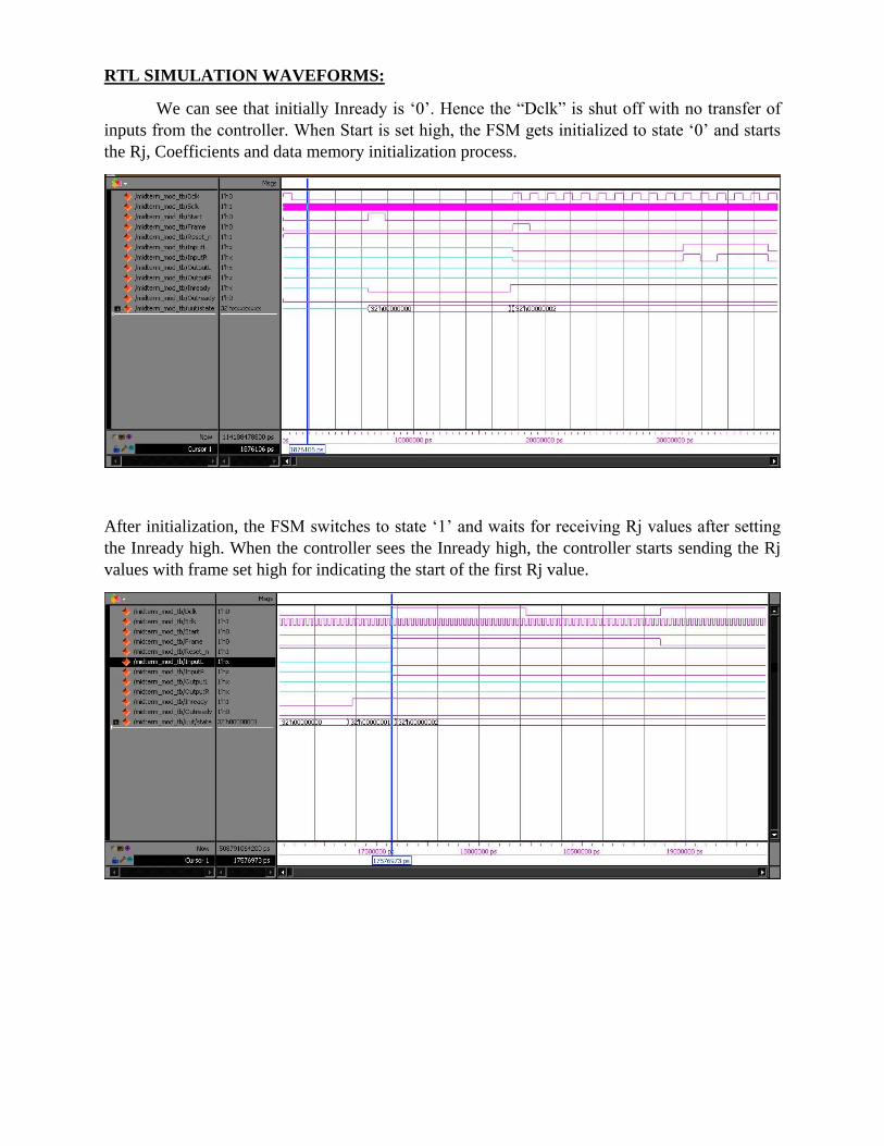
RTL SIMULATION WAVEFORMS:
We can see that initially Inready is ‘0’. Hence the “Dclk” is shut off with no transfer of
inputs from the controller. When Start is set high, the FSM gets initialized to state ‘0’ and starts
the Rj, Coefficients and data memory initialization process.
After initialization, the FSM switches to state ‘1’ and waits for receiving Rj values after setting
the Inready high. When the controller sees the Inready high, the controller starts sending the Rj
values with frame set high for indicating the start of the first Rj value.
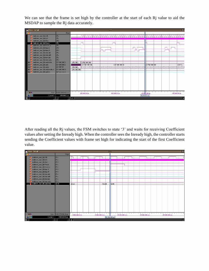
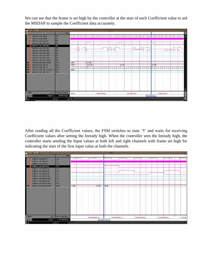
We can see that the frame is set high by the controller at the start of each Rj value to aid the
MSDAP to sample the Rj data accurately.
After reading all the Rj values, the FSM switches to state ‘3’ and waits for receiving Coefficient
values after setting the Inready high. When the controller sees the Inready high, the controller starts
sending the Coefficient values with frame set high for indicating the start of the first Coefficient
value.
We can see that the frame is set high by the controller at the start of each Coefficient value to aid
the MSDAP to sample the Coefficient data accurately.
After reading all the Coefficient values, the FSM switches to state ‘5’ and waits for receiving
Coefficient values after setting the Inready high. When the controller sees the Inready high, the
controller starts sending the Input values at both left and right channels with frame set high for
indicating the start of the first input value at both the channels.
We can see that the frame is set high by the controller at the start of each Input data value to aid
the MSDAP to sample the Input data accurately.
For going to sleep state, we used variables countL and countR to count at each zero input bit
reception at its corresponding left and right channels. The countL and countR gets resetted at any
non-zero bit reception at its corresponding left and right channels. If we are receiving 800
continuous16-bit zeros (i.e 12800 zero input bits) at both the left and right channels in the working
state, we will switch to sleep state ‘8’ and stall computing the outputs.
In the sleep state ‘8’, we constantly receive inputs without storing the data. At the first non-zero
16-bit input, we will store this data as the next input and switch to the working state ‘6’. This is
done by temporarily storing the data in the registers “tempL” and “tempR” for checking if we are
receiving a non-zero 16-bit input.
We can see that when reset is set low, Inready gets low, Dclk shuts off and stalls the controller
from sending inputs and the FSM goes to reset state ‘7’. At the reset state, all the input and output
memory gets cleared and stays in reset state until reset remains low. When reset gets high at reset
state ‘7’, the chip goes to state ‘5’ and waits for receiving input samples after setting Inready high.
When the controller sets Inready high, it starts sending the next input with the frame set high to
indicate the start of the next input. The MSDAP sees the frame set high and goes to working state
and starts reading the next inputs.
After each computation in the working state ‘6’, the corresponding output is sent at OutputL and
OutputR for the corresponding left and right channels.The MSB bit of the output is sent at the start
of the frame with Outready set high for the next 40 SClk cycles to send the corresonding 40 bit
output.
At the working state ‘6’, we can compute the first output only after receiving the first input. This
result in a delay in output computation by one input. Hence, the 512 size input data circular buffer
is not overwritten immediately after receiving the 513th input as we still need to compute the
corresponding 512th input. Hence, we temporarily store the new 513th input in the temporary
registers “DatawindtempL” and “DatawindtempR” for left and right channels correspondingly.
After the start of the 514th input, we would have completed the 513th output and hence its safe for
us to start storing the new inputs. Hence, we store the temporarily stored data as the 0th input and
start storing the 1st input in the data memory.
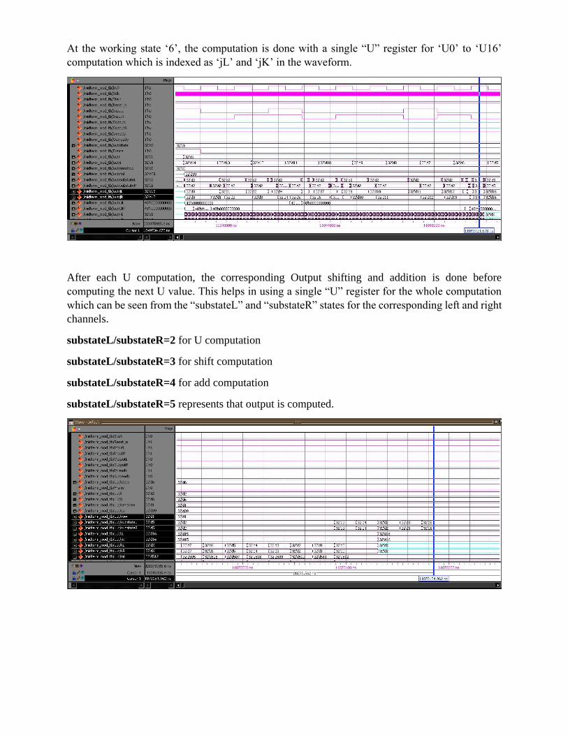
At the working state ‘6’, the computation is done with a single “U” register for ‘U0’ to ‘U16’
computation which is indexed as ‘jL’ and ‘jK’ in the waveform.
After each U computation, the corresponding Output shifting and addition is done before
computing the next U value. This helps in using a single “U” register for the whole computation
which can be seen from the “substateL” and “substateR” states for the corresponding left and right
channels.
substateL/substateR=2 for U computation
substateL/substateR=3 for shift computation
substateL/substateR=4 for add computation
substateL/substateR=5 represents that output is computed.
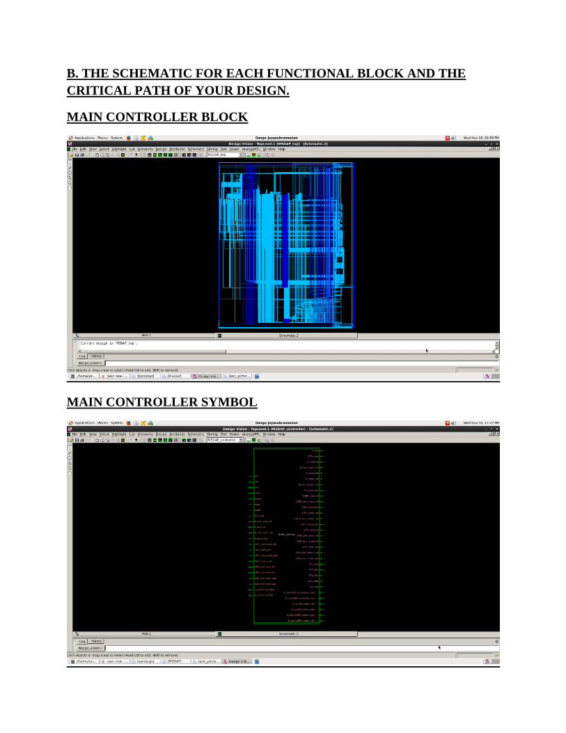
B. THE SCHEMATIC FOR EACH FUNCTIONAL BLOCK AND THE
CRITICAL PATH OF YOUR DESIGN.
MAIN CONTROLLER BLOCK
MAIN CONTROLLER SYMBOL
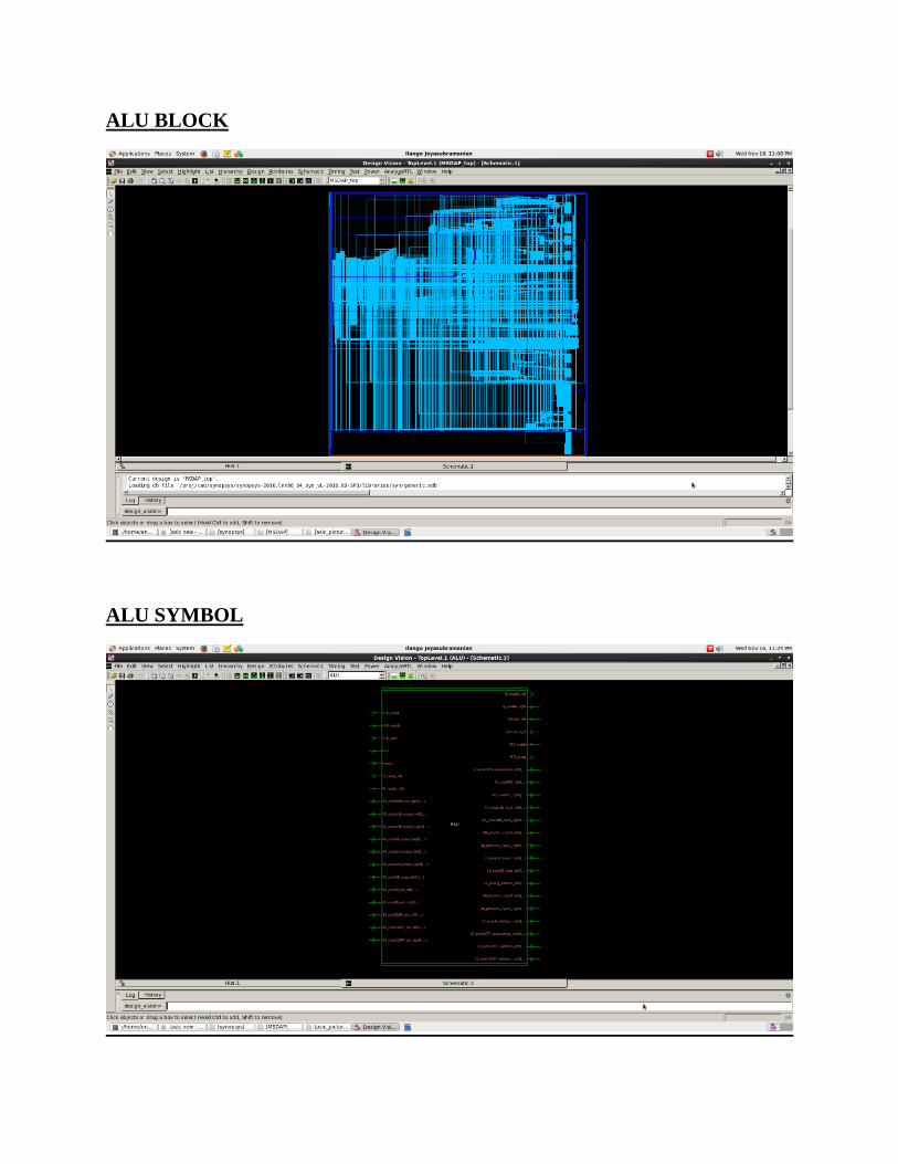
ALU BLOCK
ALU SYMBOL
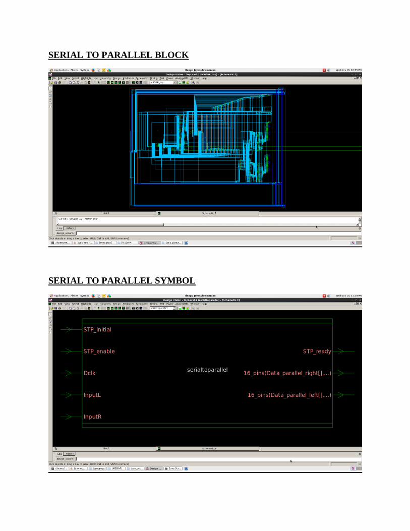
SERIAL TO PARALLEL BLOCK
SERIAL TO PARALLEL SYMBOL
PARALLEL TO SERIAL BLOCK
PARALLEL TO SERIAL SYMBOL
ADDER BLOCK
ADDER SYMBOL
SHIFTER BLOCK
SHIFTER SYMBOL
SIGN EXTENSION BLOCK
SIGN EXTENSION SYMBOL
RJ MEMORY BLOCK
RJ MEMORY SYMBOL
COEFF SYMBOL
DATA SYMBOL
GATE LEVEL SIMULATION WAVEFORMS
Start Signal:
Input Signal:
Output Signal:
Outready Signal:
Reset Signal
Sleep Signal
DESIGN VISION TIMING, CELL AND AREA REPORTS
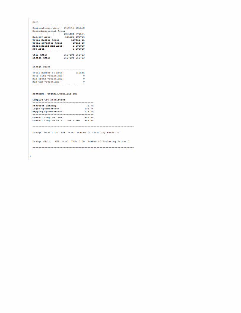
AREA REPORT
CELL REPORT
QOR REPORT
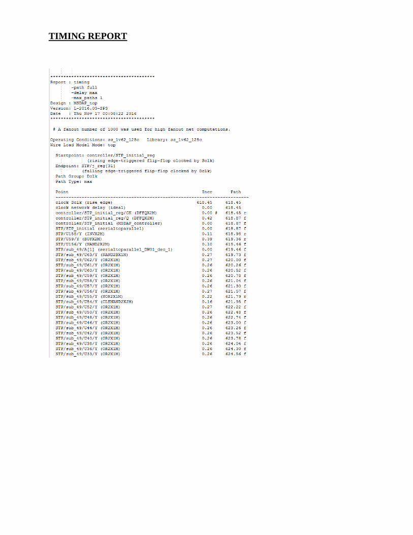
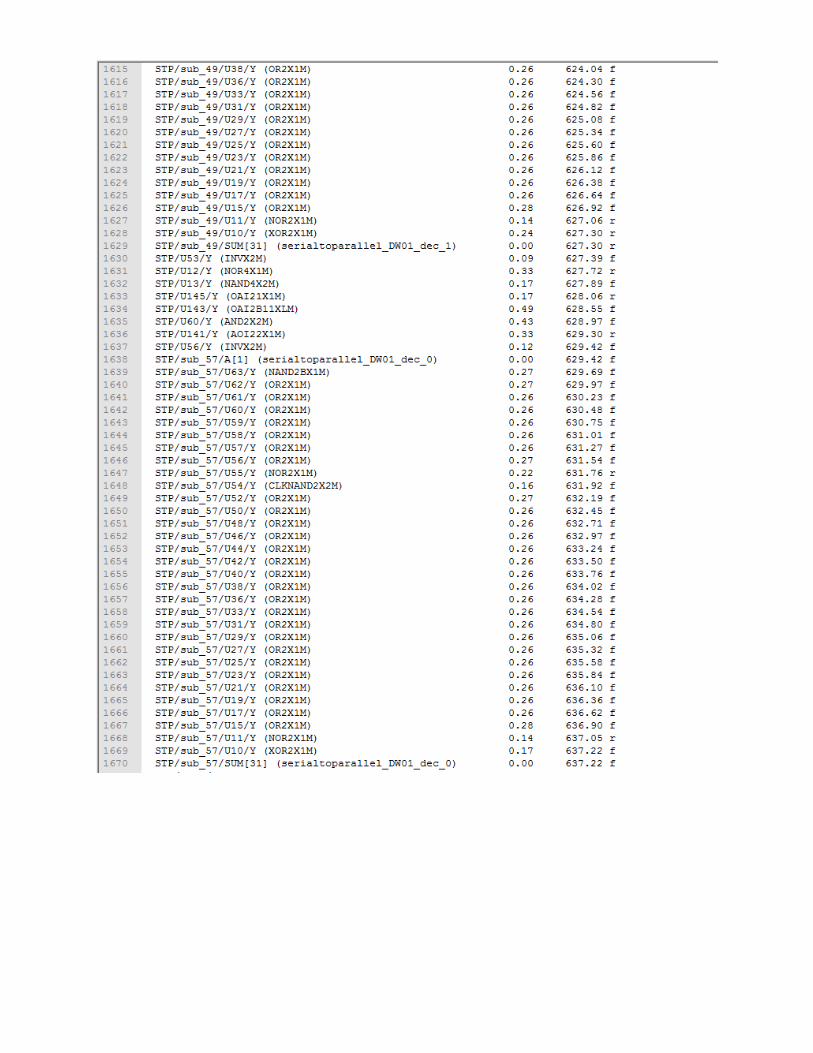
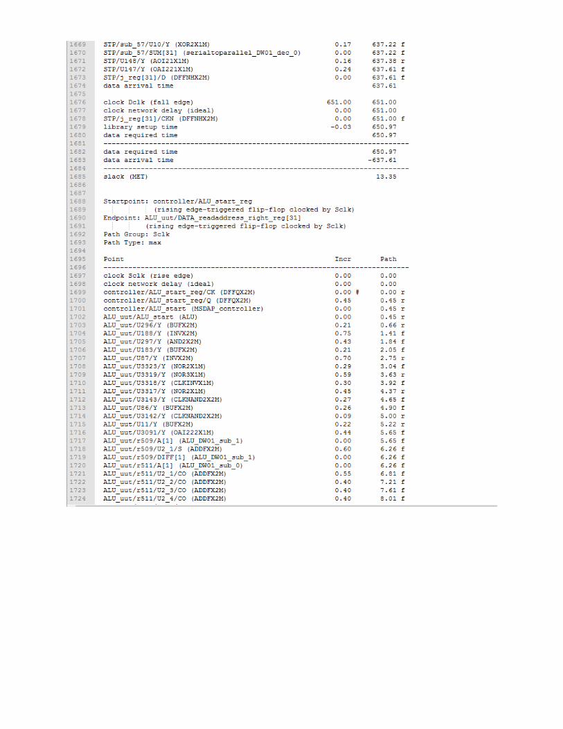
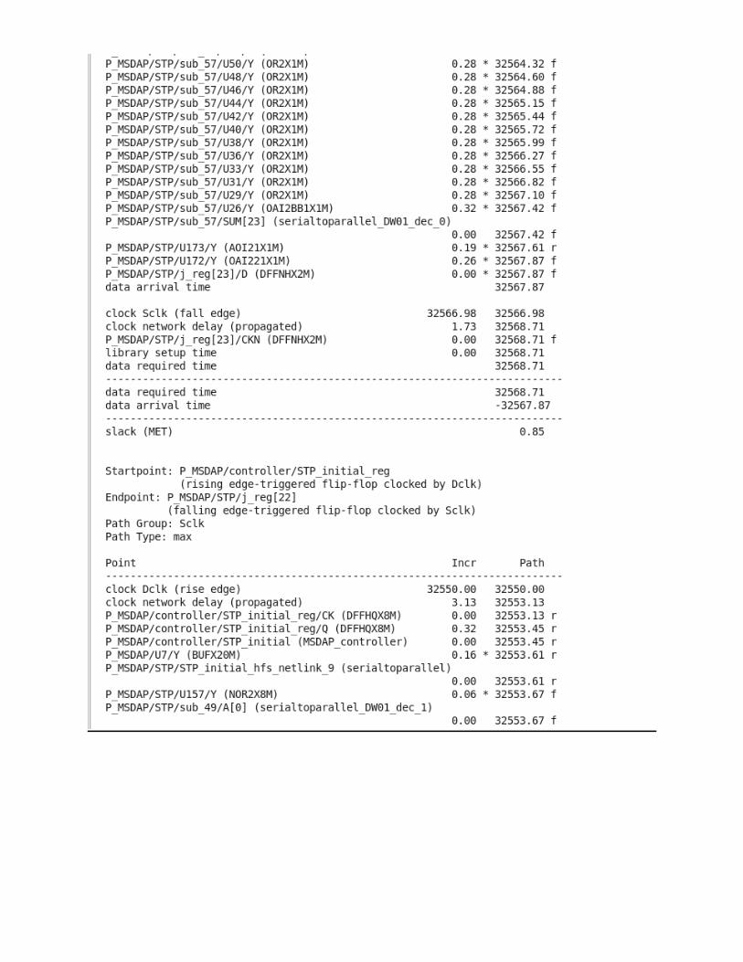
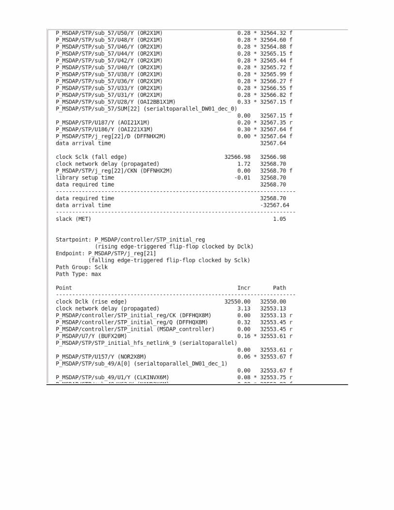
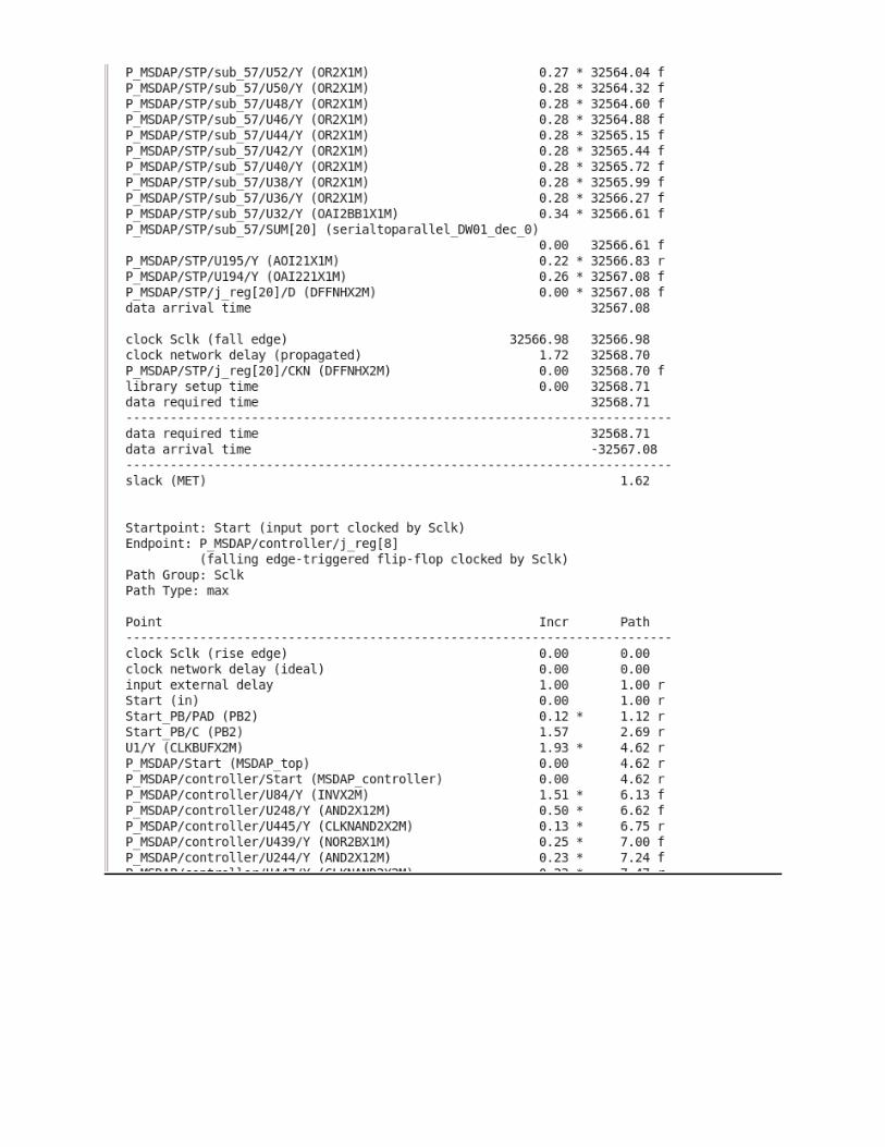
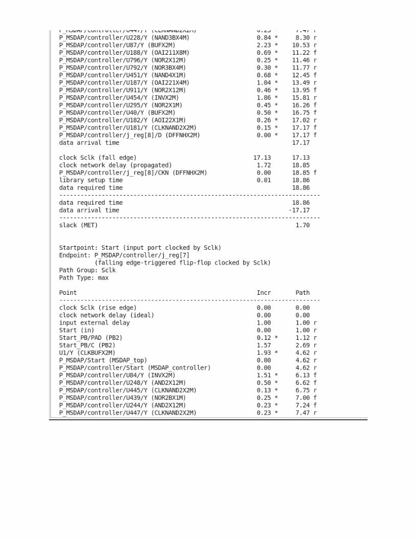
TIMING REPORT
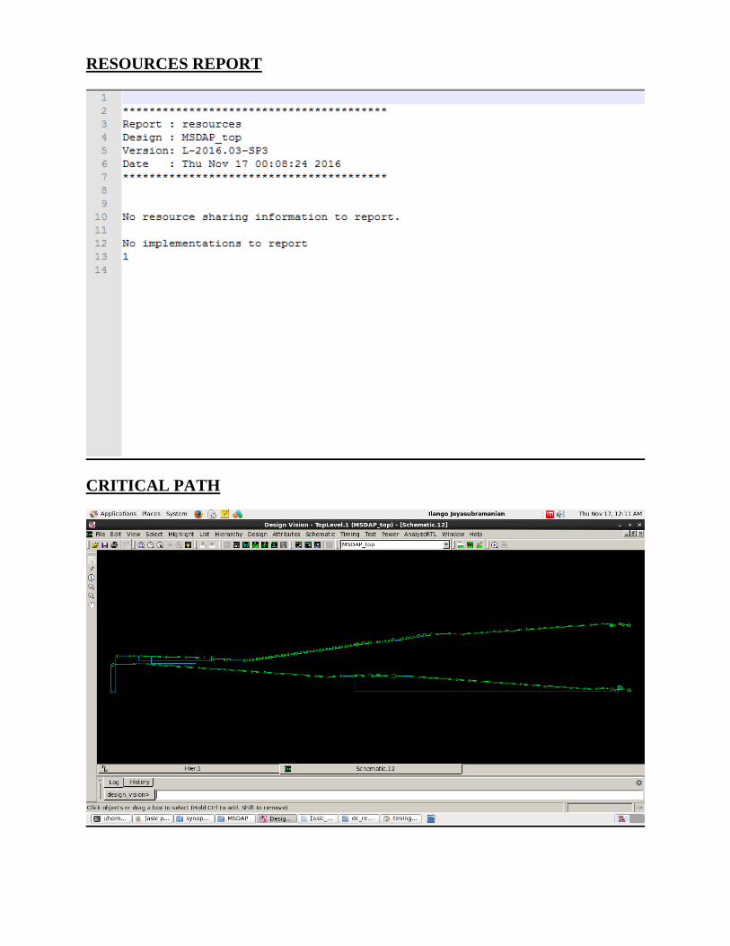
RESOURCES REPORT
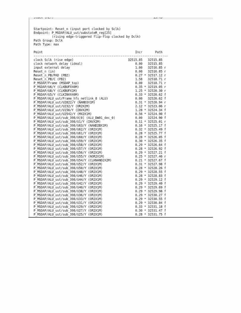
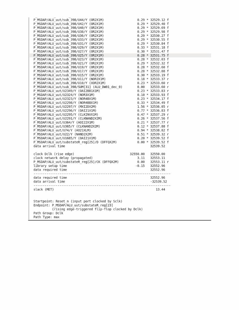
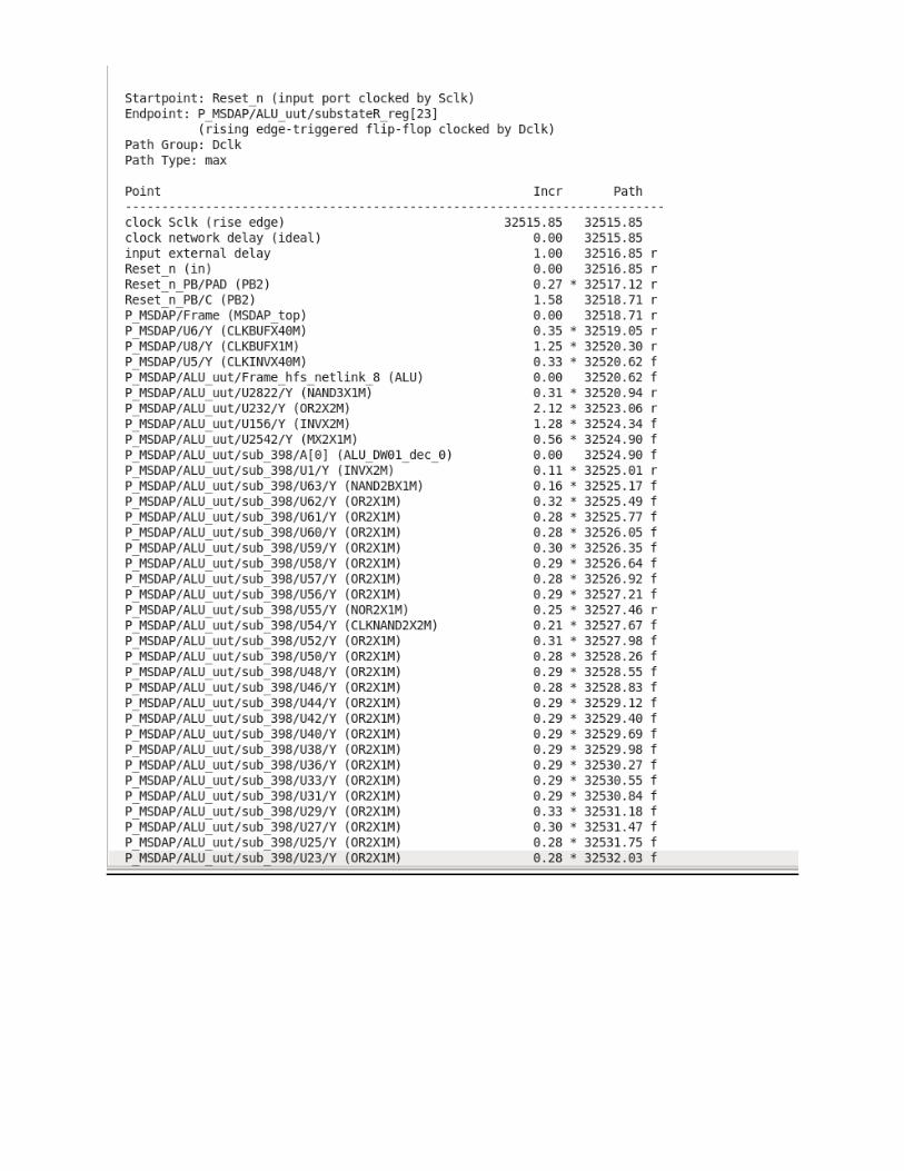
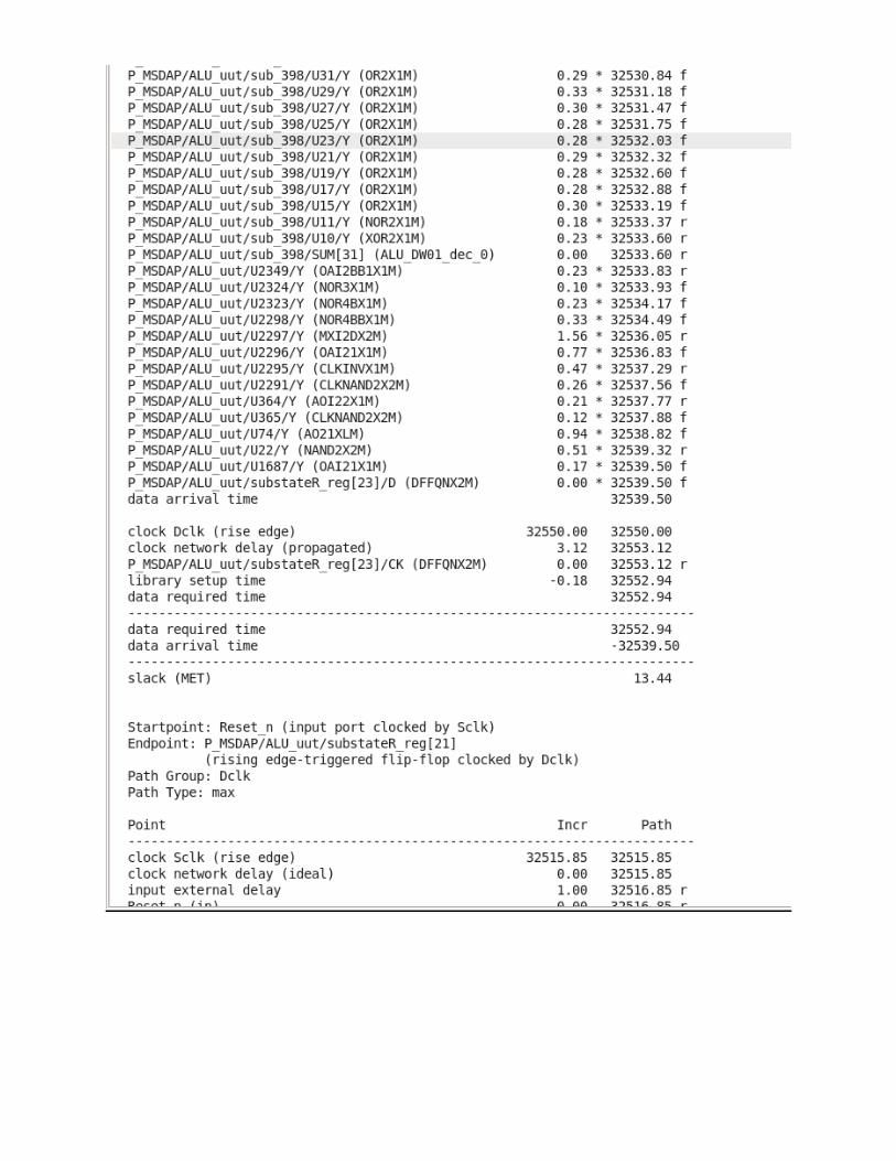
CRITICAL PATH
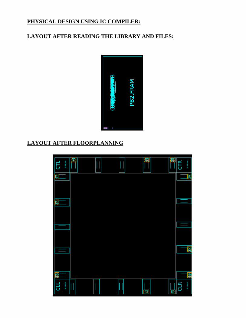
PHYSICAL DESIGN USING IC COMPILER:
LAYOUT AFTER READING THE LIBRARY AND FILES:
LAYOUT AFTER FLOORPLANNING
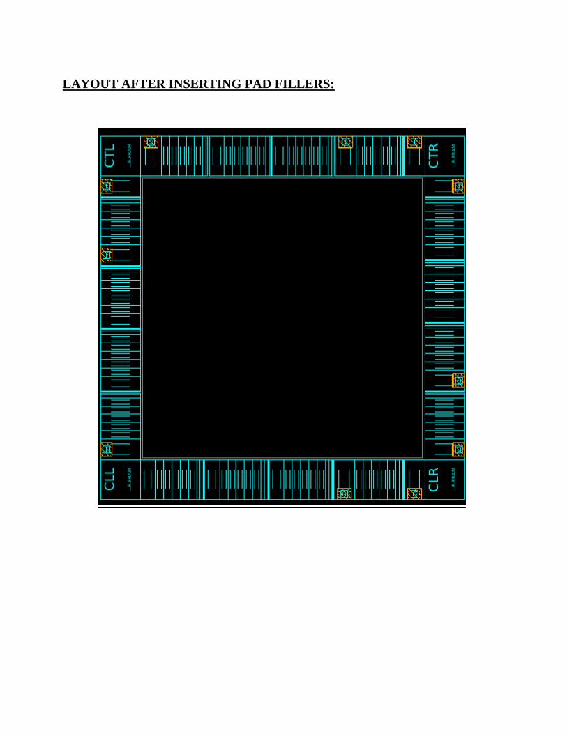
LAYOUT AFTER INSERTING PAD FILLERS:
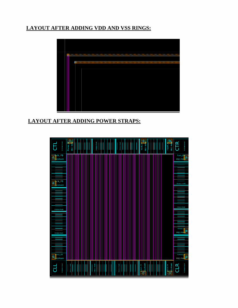
LAYOUT AFTER ADDING VDD AND VSS RINGS:
LAYOUT AFTER ADDING POWER STRAPS:
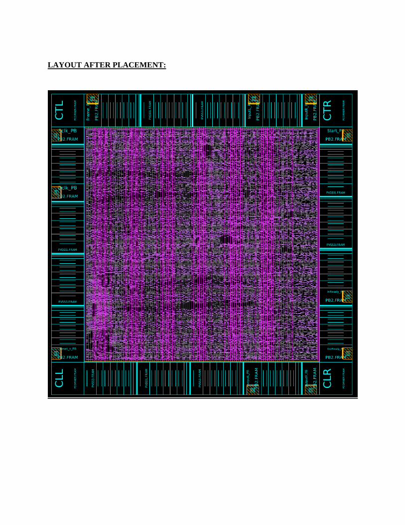
LAYOUT AFTER PLACEMENT:
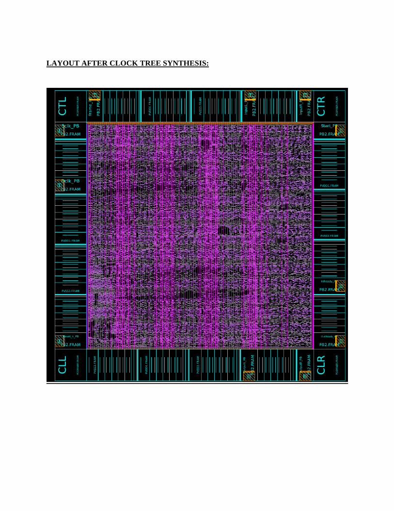
LAYOUT AFTER CLOCK TREE SYNTHESIS:
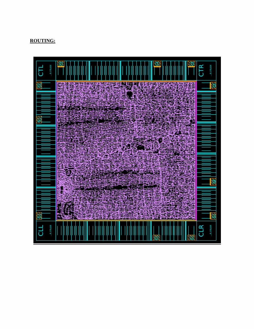
ROUTING:
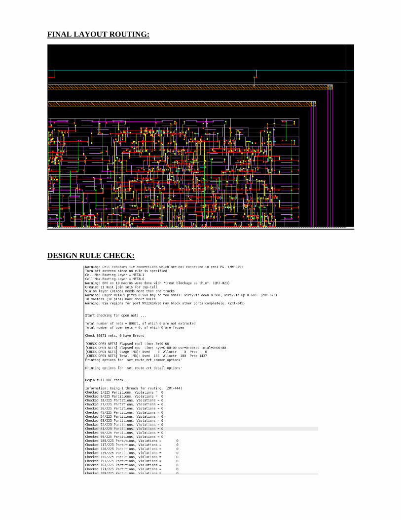
FINAL LAYOUT ROUTING:
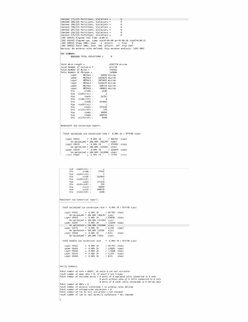
DESIGN RULE CHECK:
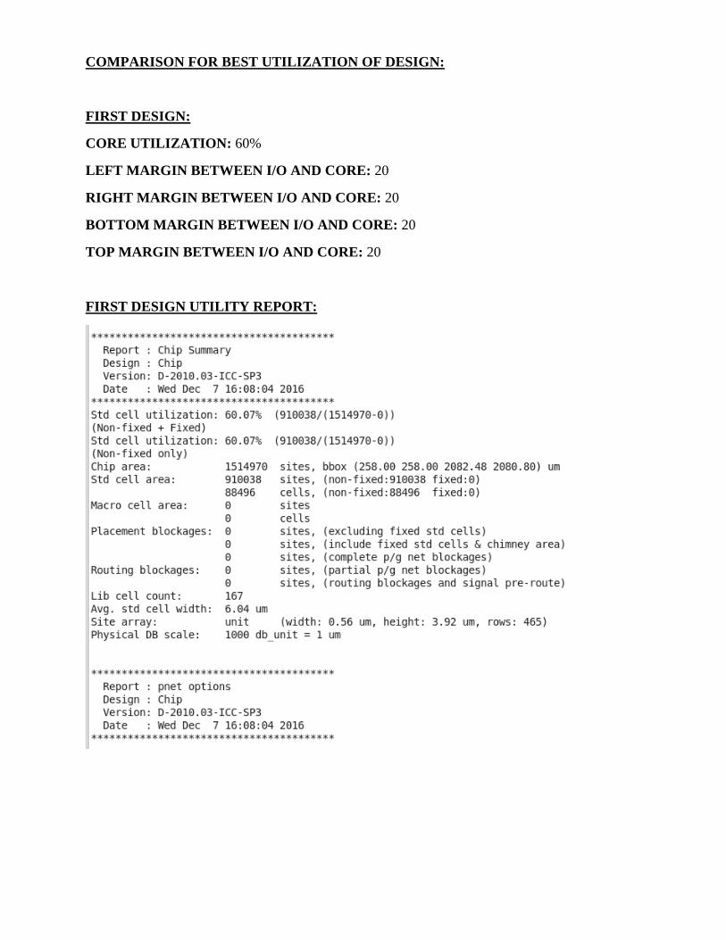
COMPARISON FOR BEST UTILIZATION OF DESIGN:
FIRST DESIGN:
CORE UTILIZATION: 60%
LEFT MARGIN BETWEEN I/O AND CORE: 20
RIGHT MARGIN BETWEEN I/O AND CORE: 20
BOTTOM MARGIN BETWEEN I/O AND CORE: 20
TOP MARGIN BETWEEN I/O AND CORE: 20
FIRST DESIGN UTILITY REPORT:
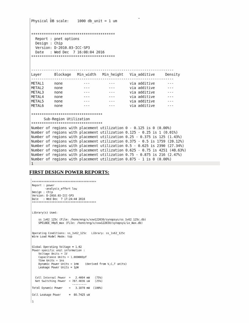
FIRST DESIGN POWER REPORTS:
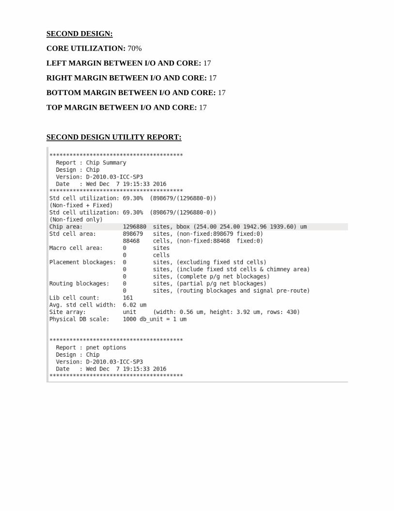
SECOND DESIGN:
CORE UTILIZATION: 70%
LEFT MARGIN BETWEEN I/O AND CORE: 17
RIGHT MARGIN BETWEEN I/O AND CORE: 17
BOTTOM MARGIN BETWEEN I/O AND CORE: 17
TOP MARGIN BETWEEN I/O AND CORE: 17
SECOND DESIGN UTILITY REPORT:
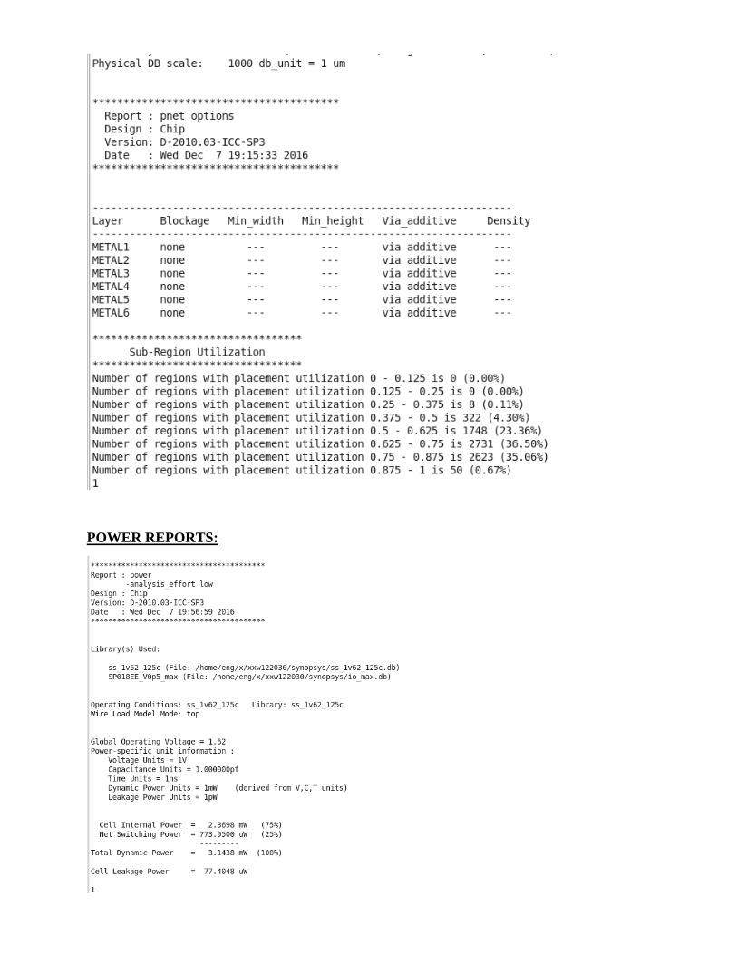
POWER REPORTS:
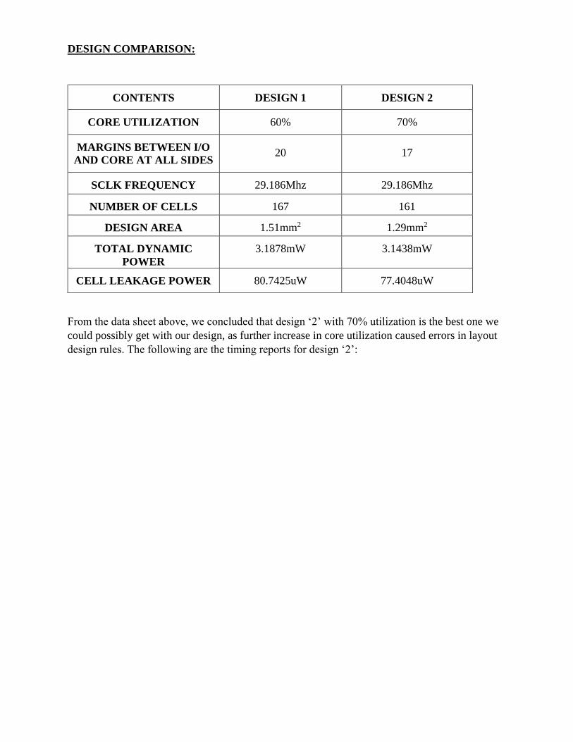
DESIGN COMPARISON:
CONTENTS DESIGN 1 DESIGN 2
CORE UTILIZATION 60% 70%
MARGINS BETWEEN I/O
AND CORE AT ALL SIDES 20 17
SCLK FREQUENCY 29.186Mhz 29.186Mhz
NUMBER OF CELLS 167 161
DESIGN AREA 1.51mm2 1.29mm2
TOTAL DYNAMIC
POWER
3.1878mW 3.1438mW
CELL LEAKAGE POWER 80.7425uW 77.4048uW
From the data sheet above, we concluded that design ‘2’ with 70% utilization is the best one we
could possibly get with our design, as further increase in core utilization caused errors in layout
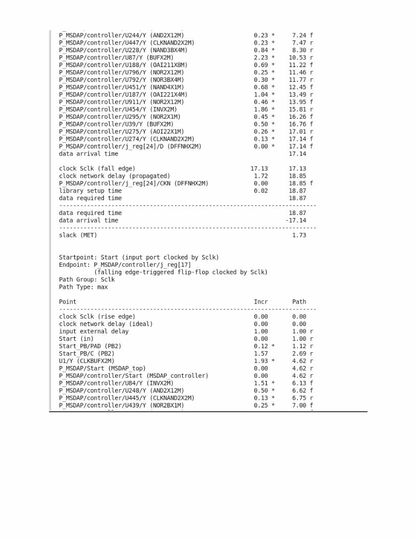
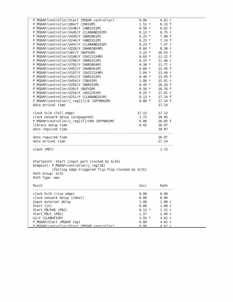
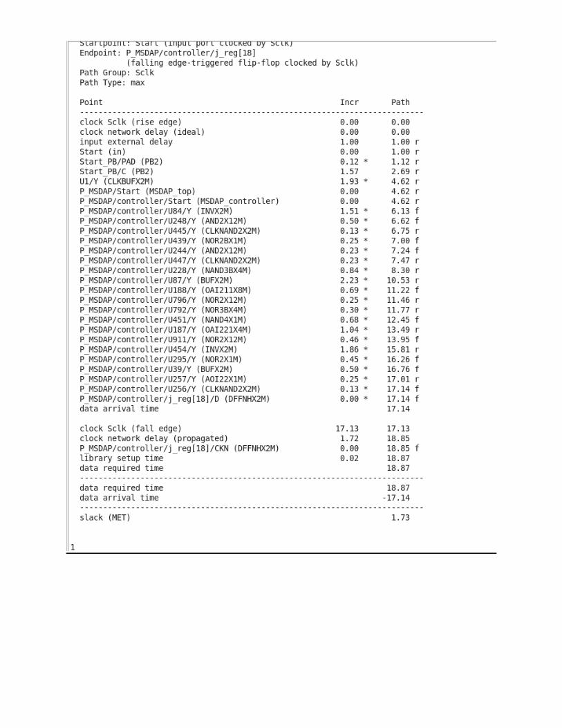
design rules. The following are the timing reports for design ‘2’:
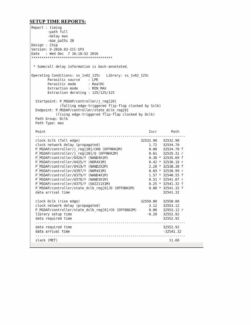
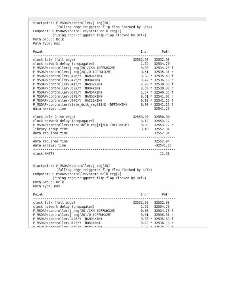
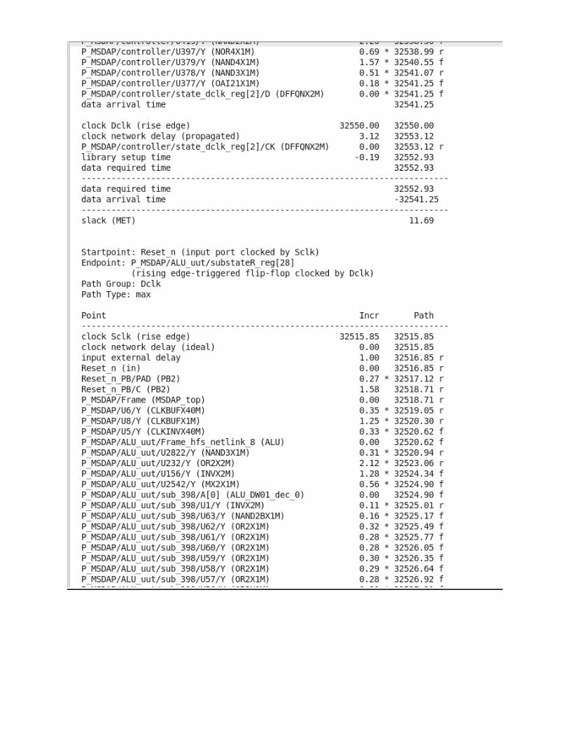
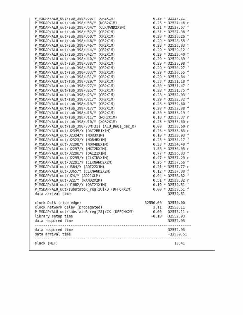
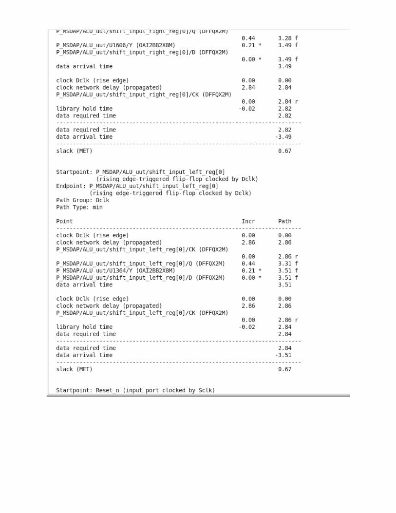
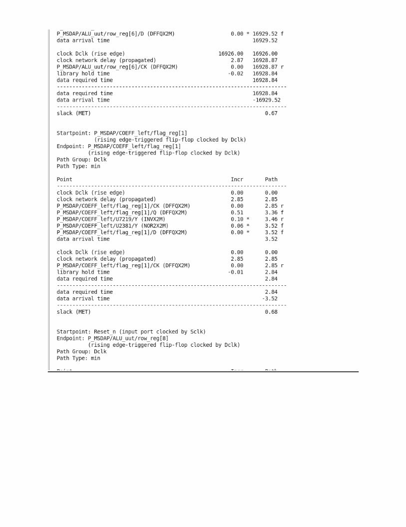
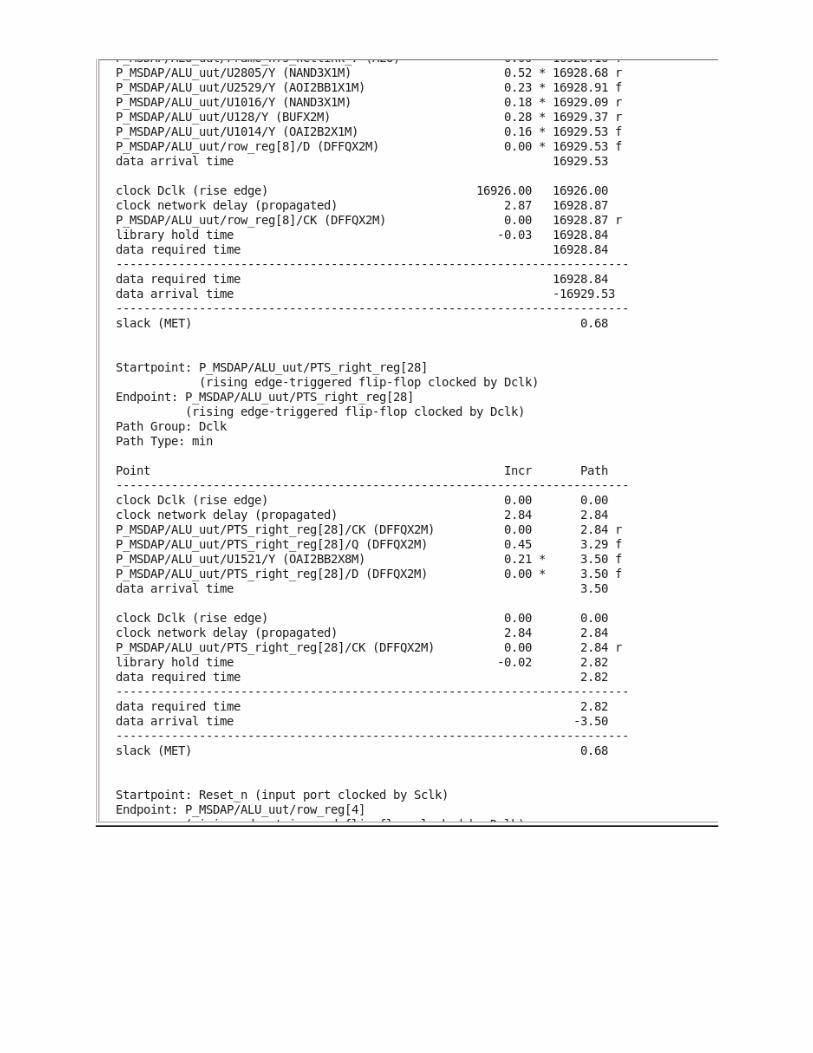
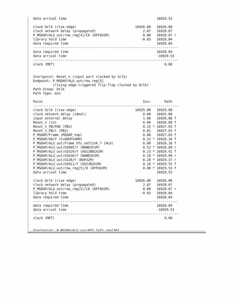
SETUP TIME REPORTS:


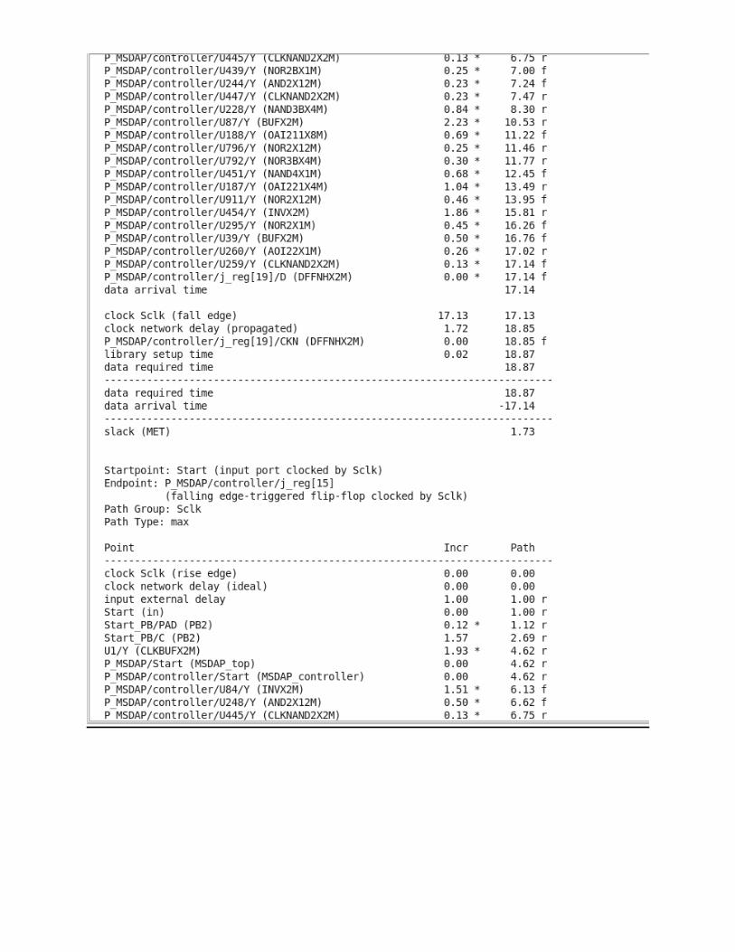
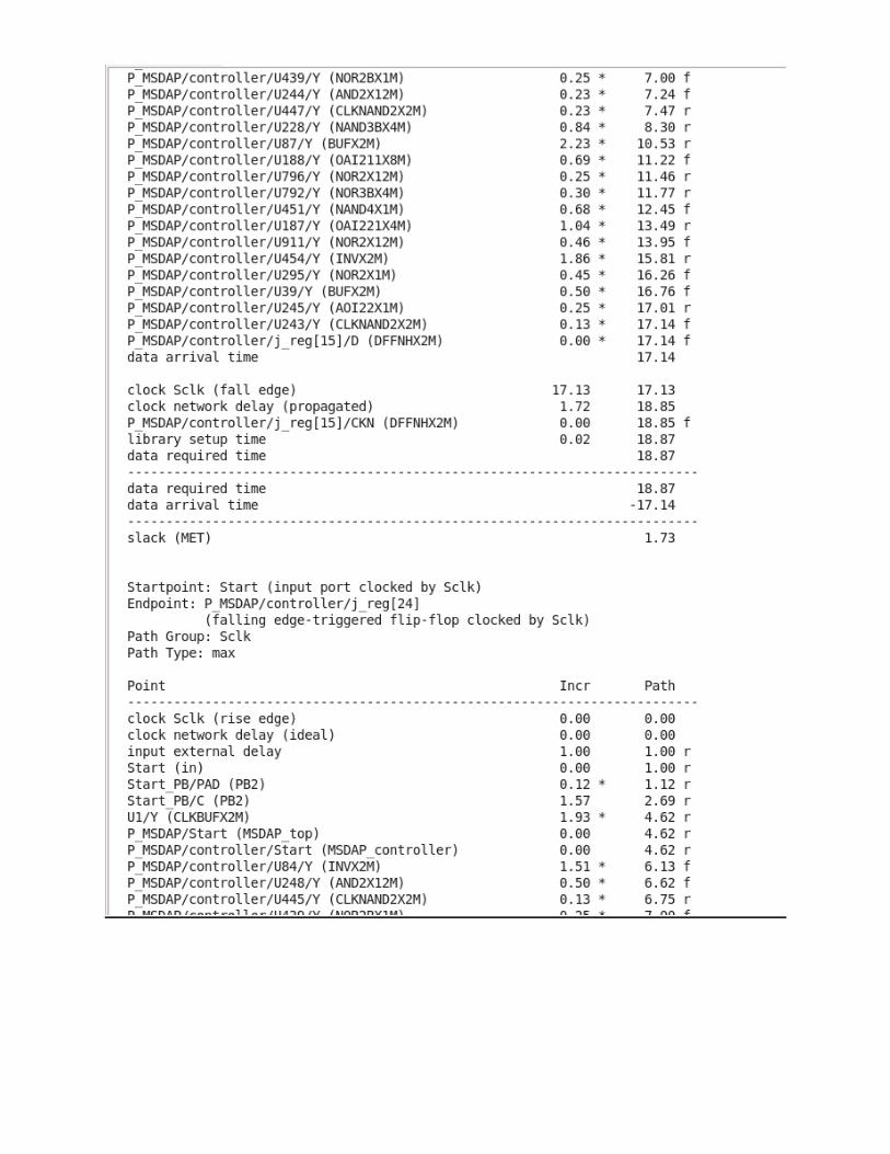
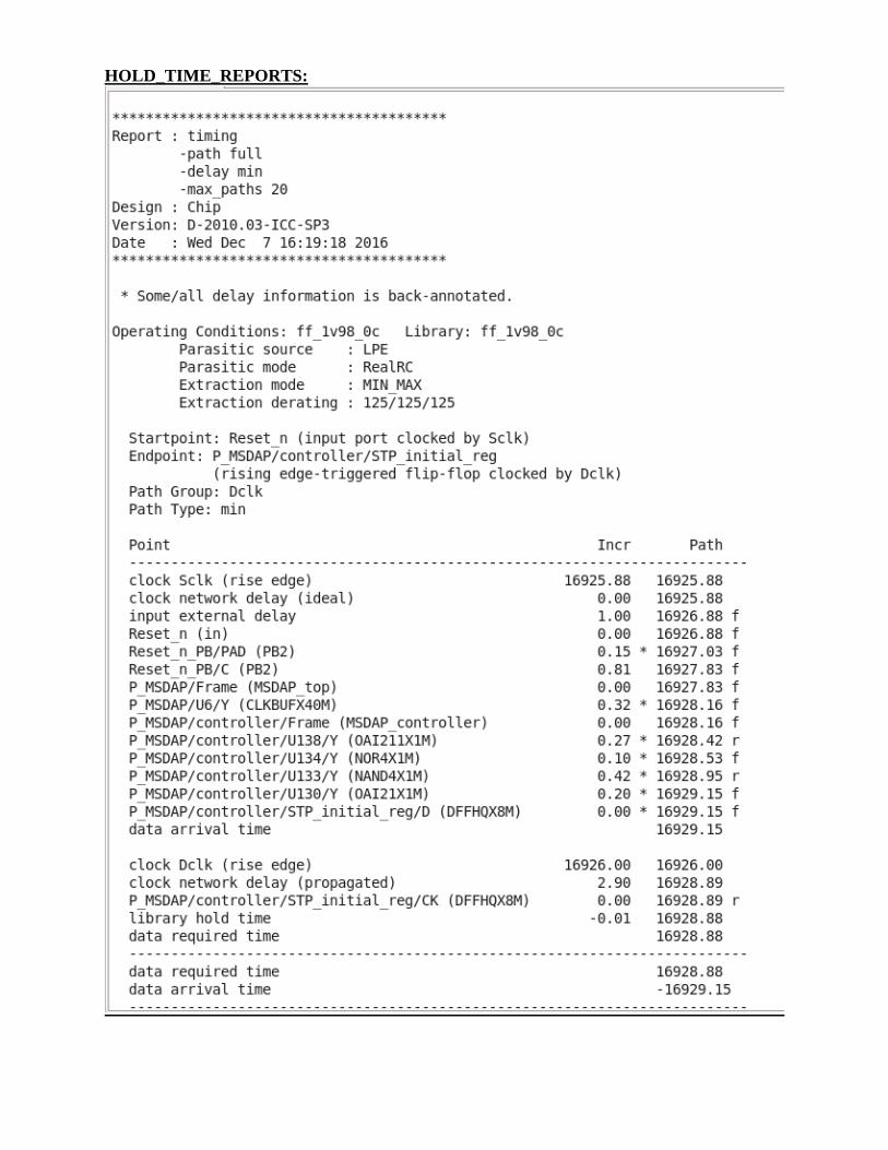
HOLD_TIME_REPORTS:


RTL_CODE:
TOP_MODULE:
`timescale 1ns / 1ps
//////////////////////////////////////////////////////////////////////////////////
// Company:
// Engineer:
//
// Create Date: 10:25:10 11/03/2016
// Design Name:
// Module Name: MSDAP_top
// Project Name:
// Target Devices:
// Tool versions:
// Description:
//
// Dependencies:
//
// Revision:
// Revision 0.01 - File Created
// Additional Comments:
//
//////////////////////////////////////////////////////////////////////////////////
module MSDAP_top(Dclk, Sclk, Start, Frame, Reset_n, InputL, InputR, OutputL, OutputR,
InReady, OutReady);
input Dclk, Sclk, Start, Frame, Reset_n;
input InputL, InputR;
output OutputL, OutputR, InReady, OutReady;
//////////////STP
wire STP_initial, STP_enable, STP_ready;
wire [15:0] Data_parallel_left, Data_parallel_right;
/////////////RJ
wire RJ_initial_left, RJ_clear_enable_left, RJ_clear_ready_left, RJ_read_enable_left,
RJ_write_enable_left, RJ_read_ready_left, RJ_write_ready_left,
RJ_initial_right, RJ_clear_enable_right, RJ_clear_ready_right, RJ_read_enable_right,
RJ_write_enable_right, RJ_read_ready_right, RJ_write_ready_right;
wire [31:0] RJ_writeaddress_left, RJ_writeaddress_right;
wire [3:0] RJ_readaddress_left, RJ_readaddress_right;
wire [15:0] RJ_out_left, RJ_out_right;
/////////////COEFF
wire COEFF_initial_left, COEFF_clear_enable_left, COEFF_clear_ready_left,
COEFF_write_enable_left, COEFF_write_ready_left,
COEFF_initial_right, COEFF_clear_enable_right, COEFF_clear_ready_right,
COEFF_write_enable_right, COEFF_write_ready_right;
wire [31:0] COEFF_writeaddress_left, COEFF_writeaddress_right;
wire [9:0] COEFF_readaddress_left, COEFF_readaddress_right;
wire [8:0] COEFF_out_left, COEFF_out_right;
////////////DATA
wire DATA_initial_left, DATA_write_enable_left, DATA_write_ready_left,
DATA_clear_enable_left, DATA_clear_ready_left,
DATA_initial_right, DATA_write_enable_right, DATA_write_ready_right,
DATA_clear_enable_right, DATA_clear_ready_right;
wire [31:0] DATA_writeaddress_left, DATA_writeaddress_right;
wire [9:0] DATA_readaddress_left, DATA_readaddress_right;
wire [15:0] DATA_out_left, DATA_out_right;
wire [31:0] count_left, count_right;
///////////SIGN EXTENSION
wire [15:0] SE_input_left, SE_input_right;
wire [39:0] SE_output_left, SE_output_right;
wire SE_initial_left, SE_initial_right;
//////////ADDER
wire AddSub_left, AddSub_right;
wire [39:0] Add_Input1_left, Add_Input1_right, Add_Input2_left, Add_Input2_right,
Add_output_left, Add_output_right;
/////////SHIFTER
wire [39:0] shift_input_left, shift_input_right, shift_output_left, shift_output_right;
wire shift_initial_left, shift_initial_right;
////////PARALLEL TO SERIAL
wire PTS_enable, PTS_ready, PTS_initial;
wire [39:0] PTS_left, PTS_right;
/////////ALU
wire ALU_enable, ALU_start, ALU_initial;
MSDAP_controller controller
(
.Dclk(Dclk),
.Sclk(Sclk),
.Start(Start),
.Frame(Frame),
.Reset_n(Reset_n),
.Inready(InReady),
.STP_enable(STP_enable),
.STP_ready(STP_ready),
.RJ_initial_left(RJ_initial_left),
.RJ_initial_right(RJ_initial_right),
.RJ_clear_enable_left(RJ_clear_enable_left),
.RJ_enable_left(RJ_write_enable_left),
.RJ_clear_ready_left(RJ_clear_ready_left),
.RJ_ready_left(RJ_write_ready_left),
.RJ_address_left(RJ_writeaddress_left),
.RJ_clear_enable_right(RJ_clear_enable_right),
.RJ_enable_right(RJ_write_enable_right),
.RJ_clear_ready_right(RJ_clear_ready_right),
.RJ_ready_right(RJ_write_ready_right),
.RJ_address_right(RJ_writeaddress_right),
.COEFF_initial_left(COEFF_initial_left),
.COEFF_initial_right(COEFF_initial_right),
.COEFF_clear_enable_left(COEFF_clear_enable_left),
.COEFF_enable_left(COEFF_write_enable_left),
.COEFF_clear_ready_left(COEFF_clear_ready_left),
.COEFF_ready_left(COEFF_write_ready_left),
.COEFF_address_left(COEFF_writeaddress_left),
.COEFF_clear_enable_right(COEFF_clear_enable_right),
.COEFF_enable_right(COEFF_write_enable_right),
.COEFF_clear_ready_right(COEFF_clear_ready_right),
.COEFF_ready_right(COEFF_write_ready_right),
.COEFF_address_right(COEFF_writeaddress_right),
.DATA_initial_left(DATA_initial_left),
.DATA_initial_right(DATA_initial_right),
.DATA_write_enable_left(DATA_write_enable_left),
.DATA_clear_enable_left(DATA_clear_enable_left),
.DATA_write_ready_left(DATA_write_ready_left),
.DATA_clear_ready_left(DATA_clear_ready_left),
.DATA_writeaddress_left(DATA_writeaddress_left),
.DATA_write_enable_right(DATA_write_enable_right),
.DATA_clear_enable_right(DATA_clear_enable_right),
.DATA_write_ready_right(DATA_write_ready_right),
.DATA_clear_ready_right(DATA_clear_ready_right),
.DATA_writeaddress_right(DATA_writeaddress_right),
.ALU_initial(ALU_initial),
.STP_initial(STP_initial),
.PTS_initial(PTS_initial),
.shift_initial_left(shift_initial_left),
.shift_initial_right(shift_initial_right),
.SE_initial_left(SE_initial_left),
.SE_initial_right(SE_initial_right),
.ALU_enable(ALU_enable),
.ALU_start(ALU_start),
.count_left(count_left),
.count_right(count_right)
);
ALU ALU_uut (
.ALU_initial(ALU_initial),
.ALU_enable(ALU_enable),
.ALU_start(ALU_start),
.Sclk(Sclk),
.Frame(Frame),
.RJ_enable_left(RJ_read_enable_left),
.RJ_enable_right(RJ_read_enable_right),
.RJ_address_left(RJ_readaddress_left),
.RJ_address_right(RJ_readaddress_right),
.RJ_ready_left(RJ_read_ready_left),
.RJ_ready_right(RJ_read_ready_right),
.RJ_out_left(RJ_out_left),
.RJ_out_right(RJ_out_right),
.COEFF_address_left(COEFF_readaddress_left),
.COEFF_address_right(COEFF_readaddress_right),
.COEFF_out_left(COEFF_out_left),
.COEFF_out_right(COEFF_out_right),
.DATA_readaddress_left(DATA_readaddress_left),
.DATA_readaddress_right(DATA_readaddress_right),
.DATA_out_left(DATA_out_left),
.DATA_out_right(DATA_out_right),
.AddSub_left(AddSub_left),
.AddSub_right(AddSub_right),
.Add_Input1_left(Add_Input1_left),
.Add_Input1_right(Add_Input1_right),
.Add_Input2_left(Add_Input2_left),
.Add_Input2_right(Add_Input2_right),
.Add_output_left(Add_output_left),
.Add_output_right(Add_output_right),
.shift_input_left(shift_input_left),
.shift_input_right(shift_input_right),
.shift_output_left(shift_output_left),
.shift_output_right(shift_output_right),
.SE_input_left(SE_input_left),
.SE_input_right(SE_input_right),
.SE_output_left(SE_output_left),
.SE_output_right(SE_output_right),
.PTS_enable(PTS_enable),
.PTS_ready(PTS_ready),
.PTS_left(PTS_left),
.PTS_right(PTS_right)
);
serialtoparallel STP
(
.STP_initial(STP_initial),
.STP_enable(STP_enable),
.STP_ready(STP_ready),
.Dclk(Dclk),
.InputL(InputL),
.InputR(InputR),
.Data_parallel_left(Data_parallel_left),
.Data_parallel_right(Data_parallel_right)
);
RJ RJ_left
(
.Sclk(Sclk),
.RJ_initial(RJ_initial_left),
.RJ_clear_enable(RJ_clear_enable_left),
.RJ_clear_ready(RJ_clear_ready_left),
.RJ_write_enable(RJ_write_enable_left),
.RJ_write_ready(RJ_write_ready_left),
.RJ_read_enable(RJ_read_enable_left),
.RJ_read_ready(RJ_read_ready_left),
.RJ_writeaddress(RJ_writeaddress_left),
.RJ_readaddress(RJ_readaddress_left),
.RJ_in(Data_parallel_left),
.RJ_out(RJ_out_left)
);
RJ RJ_right
(
.Sclk(Sclk),
.RJ_initial(RJ_initial_right),
.RJ_clear_enable(RJ_clear_enable_right),
.RJ_clear_ready(RJ_clear_ready_right),
.RJ_write_enable(RJ_write_enable_right),
.RJ_write_ready(RJ_write_ready_right),
.RJ_read_enable(RJ_read_enable_right),
.RJ_read_ready(RJ_read_ready_right),
.RJ_writeaddress(RJ_writeaddress_right),
.RJ_readaddress(RJ_readaddress_right),
.RJ_in(Data_parallel_right),
.RJ_out(RJ_out_right)
);
COEFF COEFF_left
(
.Sclk(Sclk),
.COEFF_initial(COEFF_initial_left),
.COEFF_clear_enable(COEFF_clear_enable_left),
.COEFF_clear_ready(COEFF_clear_ready_left),
.COEFF_write_enable(COEFF_write_enable_left),
.COEFF_write_ready(COEFF_write_ready_left),
.COEFF_writeaddress(COEFF_writeaddress_left),
.COEFF_readaddress(COEFF_readaddress_left),
.COEFF_in(Data_parallel_left),
.COEFF_out(COEFF_out_left)
);
COEFF COEFF_right
(
.Sclk(Sclk),
.COEFF_initial(COEFF_initial_right),
.COEFF_clear_enable(COEFF_clear_enable_right),

.COEFF_clear_ready(COEFF_clear_ready_right),
.COEFF_write_enable(COEFF_write_enable_right),
.COEFF_write_ready(COEFF_write_ready_right),
.COEFF_writeaddress(COEFF_writeaddress_right),
.COEFF_readaddress(COEFF_readaddress_right),
.COEFF_in(Data_parallel_right),
.COEFF_out(COEFF_out_right)
);
DATA DATA_left
(
.Sclk(Sclk),
.count(count_left),
.DATA_initial(DATA_initial_left),
.DATA_clear_enable(DATA_clear_enable_left),
.DATA_clear_ready(DATA_clear_ready_left),
.DATA_write_enable(DATA_write_enable_left),
.DATA_write_ready(DATA_write_ready_left),
.DATA_writeaddress(DATA_writeaddress_left),
.DATA_readaddress(DATA_readaddress_left),
.DATA_in(Data_parallel_left),
.DATA_out(DATA_out_left)
);
DATA DATA_right
(
.Sclk(Sclk),
.count(count_right),
.DATA_initial(DATA_initial_right),
.DATA_clear_enable(DATA_clear_enable_right),
.DATA_clear_ready(DATA_clear_ready_right),
.DATA_write_enable(DATA_write_enable_right),
.DATA_write_ready(DATA_write_ready_right),
.DATA_writeaddress(DATA_writeaddress_right),
.DATA_readaddress(DATA_readaddress_right),
.DATA_in(Data_parallel_right),
.DATA_out(DATA_out_right)
);
SignExtension SignExtension_left
(
.SE_initial(SE_initial_left),
.SE_input(SE_input_left),
.SE_output(SE_output_left)
);
SignExtension SignExtension_right
(
.SE_initial(SE_initial_right),
.SE_input(SE_input_right),
.SE_output(SE_output_right)
);
AdderModule ADD_left
(
.AddSub(AddSub_left),
.Input1(Add_Input1_left),
.Input2(Add_Input2_left),
.Output(Add_output_left)
);
AdderModule ADD_right
(
.AddSub(AddSub_right),
.Input1(Add_Input1_right),
.Input2(Add_Input2_right),
.Output(Add_output_right)
);
Shifter Shifter_left
(
.shift_initial(shift_initial_left),
.shift_input(shift_input_left),
.shift_output(shift_output_left)
);
Shifter Shifter_right
(
.shift_initial(shift_initial_right),
.shift_input(shift_input_right),
.shift_output(shift_output_right)
);
paralleltoserial paralleltoserial_uut
(
.PTS_initial(PTS_initial),
.PTS_enable(PTS_enable),
.PTS_ready(PTS_ready),
.Sclk(Sclk),
.Frame(Frame),
.PTS_left(PTS_left),
.PTS_right(PTS_right),
.OutputL(OutputL),
.OutputR(OutputR),
.Outready(OutReady)
);
Endmodule
MAIN CONTROLLER:
//////////////////////////////////////////////////////////////////////////////////
module MSDAP_controller
( Dclk, Sclk, Start, Frame, Reset_n, Inready,
STP_enable, STP_ready,
RJ_initial_left, RJ_clear_enable_left, RJ_clear_ready_left, RJ_enable_left,
RJ_ready_left, RJ_address_left,
RJ_initial_right, RJ_clear_enable_right, RJ_clear_ready_right, RJ_enable_right,
RJ_ready_right, RJ_address_right,
COEFF_initial_left, COEFF_clear_enable_left, COEFF_clear_ready_left,
COEFF_enable_left, COEFF_ready_left, COEFF_address_left,
COEFF_initial_right, COEFF_clear_enable_right, COEFF_clear_ready_right,
COEFF_enable_right, COEFF_ready_right, COEFF_address_right,
DATA_initial_left, DATA_write_enable_left, DATA_clear_enable_left,
DATA_write_ready_left, DATA_clear_ready_left, DATA_writeaddress_left,
DATA_initial_right, DATA_write_enable_right, DATA_clear_enable_right,
DATA_write_ready_right, DATA_clear_ready_right, DATA_writeaddress_right,
ALU_initial, STP_initial, PTS_initial, ALU_enable, ALU_start, count_left, count_right,
shift_initial_left, shift_initial_right, SE_initial_left, SE_initial_right );
input Dclk, Sclk, Start, Frame, Reset_n;
output reg Inready;
/////////STP
output reg STP_enable;
input STP_ready;
////////RJ
output reg RJ_clear_enable_left, RJ_clear_enable_right, RJ_enable_left, RJ_enable_right;
output reg [31:0] RJ_address_left, RJ_address_right;
input RJ_clear_ready_left, RJ_clear_ready_right, RJ_ready_left, RJ_ready_right;
/////////COEFF
output reg COEFF_clear_enable_left, COEFF_clear_enable_right, COEFF_enable_left,
COEFF_enable_right;
output reg [31:0] COEFF_address_left, COEFF_address_right;
input COEFF_clear_ready_left, COEFF_clear_ready_right, COEFF_ready_left,
COEFF_ready_right;
/////////DATA
output reg DATA_write_enable_left, DATA_write_enable_right, DATA_clear_enable_left,
DATA_clear_enable_right;
output reg [31:0] DATA_writeaddress_left, DATA_writeaddress_right;
input DATA_write_ready_left, DATA_write_ready_right, DATA_clear_ready_left,
DATA_clear_ready_right;
input [31:0] count_left, count_right;
/////////ALU
output reg ALU_enable, ALU_start, ALU_initial, STP_initial, PTS_initial,
RJ_initial_left, RJ_initial_right,
COEFF_initial_left, COEFF_initial_right,
DATA_initial_left, DATA_initial_right;
////////SHIFTER
output reg shift_initial_left, shift_initial_right;
////////SIGN EXTENSION
output reg SE_initial_left, SE_initial_right;
integer state_start, state_sclk, state_dclk, state_reset, i, j, flag, stop, j_temp;
wire [31:0] state_temp;
wire reset_flag;
wire [31:0] state;
reg RJ_finish, COEFF_finish, DATA_finish, miss, miss_clear;
reg [31:0] RJ_address_left_temp, RJ_address_right_temp;
reg [31:0] COEFF_address_left_temp, COEFF_address_right_temp;
reg [31:0] DATA_writeaddress_left_temp, DATA_writeaddress_right_temp;
/////////////////////start here
always@(Start)
begin
if(Start == 0)
state_start = 0;
if(Start == 1)
state_start = 1;
end
///////////////////////////////////////////////
always@(STP_ready or reset_flag or Start)
begin
//////////INITIAL
if(Start==1)
begin
RJ_enable_left = 0;
RJ_enable_right = 0;
RJ_address_left = $unsigned(-1);
RJ_address_right= $unsigned(-1);
RJ_finish = 0;
COEFF_enable_left = 0;
COEFF_enable_right = 0;
COEFF_address_left = $unsigned(-1);
COEFF_address_right= $unsigned(-1);
COEFF_finish = 0;

DATA_write_enable_left = 0;
DATA_write_enable_right = 0;
DATA_writeaddress_left = $unsigned(-1);
DATA_writeaddress_right = $unsigned(-1);
DATA_finish = 0;
miss_clear=0;
end
////////////////////////////
if(RJ_finish==0)
begin
if((RJ_ready_left==1) && (RJ_ready_right==1))
begin
RJ_enable_left = 0;
RJ_enable_right = 0;
if(RJ_address_left==15 && RJ_address_right==15)
begin
RJ_finish = 1;
RJ_address_left = $unsigned(-1);
RJ_address_right= $unsigned(-1);
end
end
if(STP_ready == 1)
begin
RJ_enable_left = 1;
RJ_enable_right = 1;
RJ_address_left_temp = RJ_address_left;
RJ_address_right_temp = RJ_address_right;
RJ_address_left = RJ_address_left_temp + 1;
RJ_address_right= RJ_address_right_temp + 1;
end
end
else if(COEFF_finish==0)
begin
if((COEFF_ready_left==1) && (COEFF_ready_right==1))
begin
COEFF_enable_left = 0;
COEFF_enable_right = 0;
if(COEFF_address_left==511 && COEFF_address_right==511)
begin
COEFF_finish = 1;
COEFF_address_left = $unsigned(-1);
COEFF_address_right= $unsigned(-1);
end
end
if(STP_ready == 1)
begin
COEFF_enable_left = 1;
COEFF_enable_right = 1;
COEFF_address_left_temp = COEFF_address_left;
COEFF_address_right_temp = COEFF_address_right;
COEFF_address_left = COEFF_address_left_temp + 1;
COEFF_address_right = COEFF_address_right_temp + 1;
end
end
else if(DATA_finish==0)
begin
if((DATA_write_ready_left == 1) && (DATA_write_ready_right == 1))
begin
DATA_write_enable_left = 0;
DATA_write_enable_right = 0;
if((DATA_writeaddress_left==511)&&(DATA_writeaddress_right==511))
begin
DATA_writeaddress_left = $unsigned(-1);
DATA_writeaddress_right = $unsigned(-1);
end
end
if(reset_flag==1)
begin
DATA_writeaddress_left = $unsigned(-2);
DATA_writeaddress_right = $unsigned(-2);
end
if(STP_ready==1 && miss==0)
begin
DATA_write_enable_left = 1;
DATA_write_enable_right = 1;
if(state==6)
begin
DATA_writeaddress_left_temp =
DATA_writeaddress_left;
DATA_writeaddress_right_temp =
DATA_writeaddress_right;
DATA_writeaddress_left =
DATA_writeaddress_left_temp + 1;
DATA_writeaddress_right =
DATA_writeaddress_right_temp + 1;
end
end
if(miss_clear==1)
miss_clear=0;
if(miss==1)
miss_clear=1;
end
end
//////////////////////////////////Sclk work here
always@(posedge Sclk)
begin
///////////INITIAL
if(Start==0)
begin
RJ_initial_left =0;
RJ_initial_right=0;
COEFF_initial_left =0;
COEFF_initial_right=0;
DATA_initial_left =0;
DATA_initial_right=0;
end
if(Start==1)
begin
miss=0;
state_sclk = 0;
state_dclk = 0;
flag = 0;
stop=0;
STP_enable = 0;
ALU_initial= 0;
STP_initial= 0;
PTS_initial= 0;
RJ_initial_left =1;
RJ_initial_right =1;
COEFF_initial_left =1;
COEFF_initial_right=1;
DATA_initial_left =1;
DATA_initial_right =1;
ALU_enable = 0;
ALU_start = 0;
RJ_clear_enable_left = 0;
RJ_clear_enable_right = 0;
COEFF_clear_enable_left = 0;
COEFF_clear_enable_right = 0;
DATA_clear_enable_left = 0;
DATA_clear_enable_right = 0;
end
////////////////////////////
if(miss_clear==1)
miss=0;
/////////////////RESET READY
if(RJ_clear_ready_left==1 && RJ_clear_ready_right==1)
begin
RJ_clear_enable_left = 0;
RJ_clear_enable_right = 0;
end
if(COEFF_clear_ready_left==1 && COEFF_clear_ready_right==1)
begin
COEFF_clear_enable_left = 0;
COEFF_clear_enable_right = 0;
end
if(DATA_clear_ready_left==1 && DATA_clear_ready_right==1)
begin
DATA_clear_enable_left = 0;
DATA_clear_enable_right = 0;
end
//////////STATE MACHINE
case(state)
0:
begin
Inready = 0;
RJ_clear_enable_left = 1;
RJ_clear_enable_right = 1;
COEFF_clear_enable_left = 1;
COEFF_clear_enable_right= 1;
DATA_clear_enable_left = 1;
DATA_clear_enable_right = 1;
ALU_initial=1;
PTS_initial=1;
shift_initial_left = 1;
shift_initial_right = 1;
SE_initial_left = 1;
SE_initial_right = 1;
if(DATA_clear_ready_left==1 && DATA_clear_ready_right==1)
begin
state_sclk =1;
ALU_initial=0;
PTS_initial=0;
end
end
1:
begin
Inready = 1;
if(Frame == 1)
begin
state_sclk = 2;
end
end
2:
begin
if(Frame==0 && STP_initial==1)
STP_initial=0;
if(Frame==1 && RJ_address_left==-1 && stop==0)
begin
STP_initial=1;
stop=1;
end
if(Frame == 1)
STP_enable = 1;
if(STP_enable == 1 && Frame==0)
STP_enable = 0;
if(RJ_address_left==14 && RJ_address_right==14 && j==-1)
state_dclk = 3;
end
3:
begin
Inready = 1;
if(Frame == 1)
begin
state_sclk = 4;
end
end
4:
begin
if(Frame == 1)
STP_enable = 1;
if(STP_enable == 1 && Frame==0)
STP_enable = 0;
if(COEFF_address_left==510 && COEFF_address_right==510 && j==-
1)
state_dclk = 5;
end
5:
begin
Inready = 1;
ALU_enable = 0;
if(Frame == 1)
begin
state_sclk = 6;
flag = 0;
end
end
6:
begin
state_sclk = 0;
if(Frame == 1)
STP_enable = 1;
if(STP_enable == 1 && Frame==0)
STP_enable = 0;
if(ALU_start == 1)
ALU_start = 0;
if(Frame == 1 && DATA_writeaddress_left==0 && flag==0)
begin
ALU_enable = 1;
ALU_start = 1;
flag = 1;
end
if(Frame==1 && count_left>=800 && count_right>=800 && j==14)
begin
state_sclk = 8;
ALU_enable = 0;
end
end
7:
begin
Inready = 0;
DATA_clear_enable_left = 1;
DATA_clear_enable_right = 1;
miss = 1;
end
8:
begin
if(Frame == 1'b1)
STP_enable = 1'b1;
if(STP_enable == 1 && Frame==0)
STP_enable = 0;
if(count_left==0 || count_right==0)
begin
state_sclk = 6;
ALU_enable = 1;
end
end
endcase
end
///////////////////////////////Dclk work here
always@(negedge Dclk)
begin
case(state)
2:
begin
if(Frame == 1'b1)
j=15;
if(j>=0)
begin
j_temp = j;
j = j_temp - 1;
end
end
4:
begin
if(Frame == 1'b1)
j=15;
if(j>=0)
begin
j_temp = j;
j = j_temp - 1;
end
end
6:
begin
if(Frame == 1'b1)
j=15;
if(j>=0)
begin
j_temp = j;
j = j_temp - 1;
end
end
endcase
end
///////////////////////Reset check here
always@(Reset_n or Start)
begin
///////////INITIAL
if(Start==1)
state_reset = 0;
//////////////////
case(state)
5:
begin
if(Reset_n == 0)
begin
state_reset = 7;
end
end
6:
begin
if(Reset_n == 0)
begin
state_reset = 7;
end
end
7:
begin
if(Reset_n == 1)
begin
state_reset = 5;
end
if(Reset_n == 0)
begin
state_reset = 7;
end
end
8:
begin
if(Reset_n == 0)
begin
state_reset = 7;
end
end
endcase
end
assign reset_flag = (state==5 && Reset_n == 1)? 1 : 0;
assign state_temp = state;
assign state = ((state_start==1) ? 0 :
((state==0 && state_sclk ==1)? 1 :
((state==1 && state_sclk ==2)? 2 :
((state==2 && state_dclk ==3)? 3 :
((state==3 && state_sclk ==4)? 4 :
((state==4 && state_dclk ==5)? 5 :
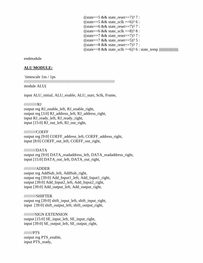
((state==5 && state_reset==7)? 7 :
((state==5 && state_sclk ==6)? 6 :
((state==6 && state_reset==7)? 7 :
((state==6 && state_sclk ==8)? 8 :
((state==7 && state_reset==7)? 7 :
((state==7 && state_reset==5)? 5 :
((state==8 && state_reset==7)? 7 :
((state==8 && state_sclk ==6)? 6 : state_temp ))))))))))))));
endmodule
ALU MODULE:
`timescale 1ns / 1ps
//////////////////////////////////////////////////////////////////////////////////
module ALU(
input ALU_initial, ALU_enable, ALU_start, Sclk, Frame,
////////////RJ
output reg RJ_enable_left, RJ_enable_right,
output reg [3:0] RJ_address_left, RJ_address_right,
input RJ_ready_left, RJ_ready_right,
input [15:0] RJ_out_left, RJ_out_right,
///////////COEFF
output reg [9:0] COEFF_address_left, COEFF_address_right,
input [8:0] COEFF_out_left, COEFF_out_right,
///////////DATA
output reg [9:0] DATA_readaddress_left, DATA_readaddress_right,
input [15:0] DATA_out_left, DATA_out_right,
///////////ADDER
output reg AddSub_left, AddSub_right,
output reg [39:0] Add_Input1_left, Add_Input1_right,
output [39:0] Add_Input2_left, Add_Input2_right,
input [39:0] Add_output_left, Add_output_right,
///////////SHIFTER
output reg [39:0] shift_input_left, shift_input_right,
input [39:0] shift_output_left, shift_output_right,
//////////SIGN EXTENSION
output [15:0] SE_input_left, SE_input_right,
input [39:0] SE_output_left, SE_output_right,
////////PTS
output reg PTS_enable,
input PTS_ready,
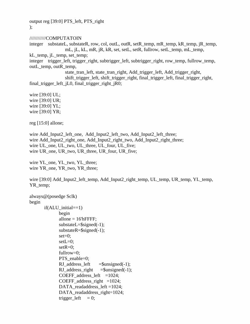
output reg [39:0] PTS_left, PTS_right
);
////////////COMPUTATOIN
integer substateL, substateR, row, col, outL, outR, setR_temp, mR_temp, kR_temp, jR_temp,
mL, jL, kL, mR, jR, kR, set, setL, setR, fullrow, setL_temp, mL_temp,
kL_temp, jL_temp, set_temp;
integer trigger_left, trigger_right, subtrigger_left, subtrigger_right, row_temp, fullrow_temp,
outL_temp, outR_temp,
state_tran_left, state_tran_right, Add_trigger_left, Add_trigger_right,
shift_trigger_left, shift_trigger_right, final_trigger_left, final_trigger_right,
final_trigger_left_jL0, final_trigger_right_jR0;
wire [39:0] UL;
wire [39:0] UR;
wire [39:0] YL;
wire [39:0] YR;
reg [15:0] allone;
wire Add_Input2_left_one, Add_Input2_left_two, Add_Input2_left_three;
wire Add_Input2_right_one, Add_Input2_right_two, Add_Input2_right_three;
wire UL_one, UL_two, UL_three, UL_four, UL_five;
wire UR_one, UR_two, UR_three, UR_four, UR_five;
wire YL_one, YL_two, YL_three;
wire YR_one, YR_two, YR_three;
wire [39:0] Add_Input2_left_temp, Add_Input2_right_temp, UL_temp, UR_temp, YL_temp,
YR_temp;
always@(posedge Sclk)
begin
if(ALU_initial==1)
begin
allone = 16'hFFFF;
substateL=$signed(-1);
substateR=$signed(-1);
set=0;
setL=0;
setR=0;
fullrow=0;
PTS_enable=0;
RJ_address_left =$unsigned(-1);
RJ_address_right =$unsigned(-1);
COEFF_address_left =1024;
COEFF_address_right =1024;
DATA_readaddress_left =1024;
DATA_readaddress_right=1024;
trigger_left = 0;
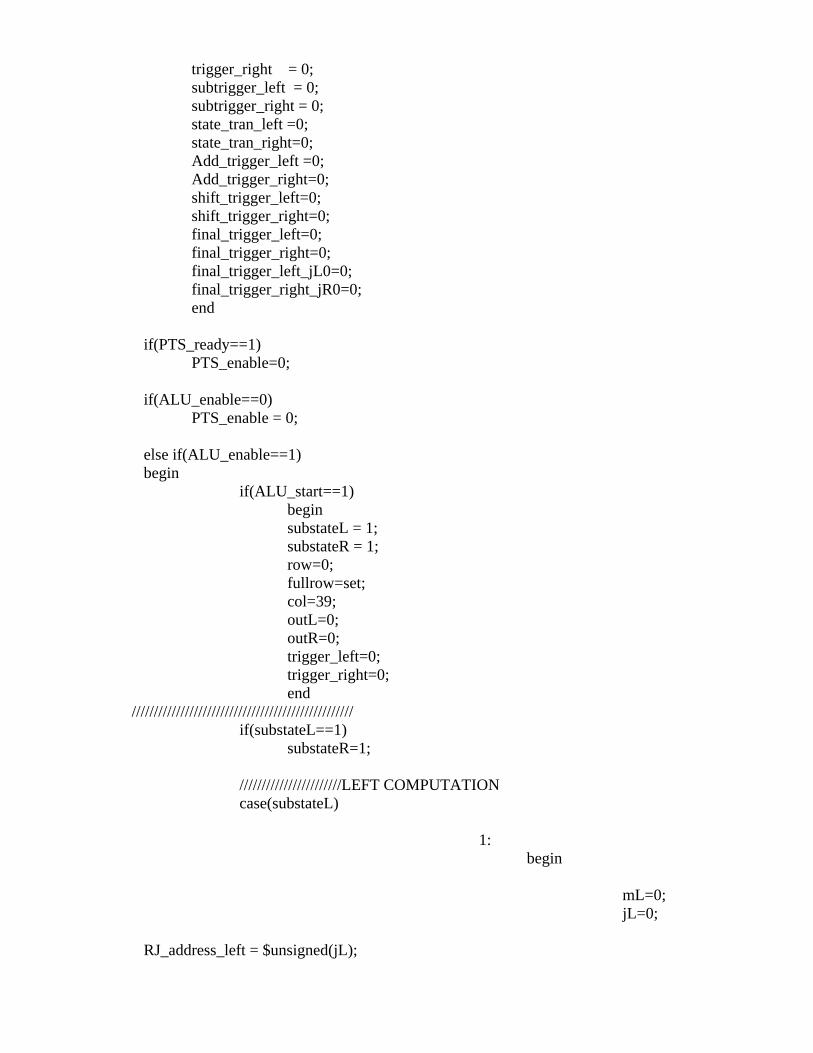
trigger_right = 0;
subtrigger_left = 0;
subtrigger_right = 0;
state_tran_left =0;
state_tran_right=0;
Add_trigger_left =0;
Add_trigger_right=0;
shift_trigger_left=0;
shift_trigger_right=0;
final_trigger_left=0;
final_trigger_right=0;
final_trigger_left_jL0=0;
final_trigger_right_jR0=0;
end
if(PTS_ready==1)
PTS_enable=0;
if(ALU_enable==0)
PTS_enable = 0;
else if(ALU_enable==1)
begin
if(ALU_start==1)
begin
substateL = 1;
substateR = 1;
row=0;
fullrow=set;
col=39;
outL=0;
outR=0;
trigger_left=0;
trigger_right=0;
end
//////////////////////////////////////////////////
if(substateL==1)
substateR=1;
///////////////////////LEFT COMPUTATION
case(substateL)
1:
begin
mL=0;
jL=0;
RJ_address_left = $unsigned(jL);
substateL = 2;
state_tran_left=1;
end
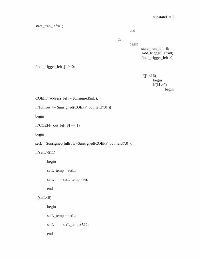
2:
begin
state_tran_left=0;
Add_trigger_left=0;
final_trigger_left=0;
final_trigger_left_jL0=0;
if(jL<16)
begin
if(kL>0)
begin
COEFF_address_left = $unsigned(mL);
if(fullrow >= $unsigned(COEFF_out_left[7:0]))
begin
if(COEFF_out_left[8] == 1)
begin
setL = $unsigned(fullrow)-$unsigned(COEFF_out_left[7:0]);
if(setL>511)
begin
setL_temp = setL;
setL = setL_temp - set;
end
if(setL<0)
begin
setL_temp = setL;
setL = setL_temp+512;
end
DATA_readaddress_left = $unsigned(setL);
AddSub_left = 1;
Add_Input1_left = UL;
Add_trigger_left=1;
end
else
begin
setL = $unsigned(fullrow-COEFF_out_left[7:0]);
if(setL>511)
begin
setL_temp = setL;
setL = setL_temp - set;
end
if(setL<0)
begin
setL_temp = setL;
setL = setL_temp+512;
end
DATA_readaddress_left = $unsigned(setL);
AddSub_left = 0;
Add_Input1_left = UL;
Add_trigger_left=1;
end
end
mL_temp = mL;
mL
= mL_temp + 1;
kL_temp = kL;
kL
= kL_temp - 1;
end
end
if(trigger_left==0)
begin
kL =
$signed(RJ_out_left);
trigger_left=1;
end
if(jL==16)
begin
substateL = 3;
trigger_left=0;
end
if(kL==0)
begin
substateL = 3;
trigger_left=0;
end
end
3:
begin
Add_trigger_left=0;
if(jL<=16 &&
jL>0)
begin
shift_input_left = YL;
shift_trigger_left=1;
end
substateL = 4;
end
4:
begin
shift_trigger_left=0;
if(jL<=16 &&
jL>0)
begin
AddSub_left = 0;
Add_Input1_left = YL;
final_trigger_left=1;
end
final_trigger_left_jL0=1;
jL_temp = jL;;
jL =
jL_temp + 1;
if(jL==17)
substateL = 5;
else
begin
RJ_address_left = $unsigned(jL);
substateL = 2;
end
end
5: //OUTPUT SIDE
begin
if(Frame==0 &&
trigger_left==0)
begin
PTS_enable =
1;
PTS_left =
YL;
PTS_right=
YR;
end
if(Frame==1 && row
<= 511 && trigger_left == 0)
begin
trigger_left =
1;
row_temp =
row;
row =
row_temp + 1;
fullrow_temp
= fullrow;
fullrow =
fullrow_temp + 1;
outL_temp =
outL;
outL =
outL_temp + 1;
outR_temp =
outR;
outR =
outR_temp + 1;
if(outL==2)
outL=0;
if(outR==2)
outR=0;
mL=0;
mR=0;
jL=0;
jR=0;
end
if(trigger_left == 1)
begin
RJ_enable_left
= 1;
RJ_address_left = $unsigned(jL);
RJ_enable_right = 1;
RJ_address_right = $unsigned(jR);
if(RJ_ready_left==1 && RJ_ready_right==1 && Frame==0)
begin
RJ_enable_left = 0;
RJ_enable_right = 0;
kL =
$signed(RJ_out_left);
kR =
$signed(RJ_out_right);
substateL = 1;
trigger_left = 0;
end
end
if(row==512)
begin
row=0;
set_temp =
set;
set =
set_temp + 512;
end
if(fullrow==7000)
begin
substateL = 6;
substateR = 6;
end
end
endcase
//////////RIGHT COMPUTATION
case(substateR)
1:
begin
mR=0;
jR=0;
RJ_enable_right = 1;
RJ_address_right =
$unsigned(jR);
substateR = 2;
state_tran_right=1;
end
2:
begin
state_tran_right=0;
Add_trigger_right=0;
final_trigger_right=0;
final_trigger_right_jR0=0;
if(jR<16)
begin
if(kR>0)
begin
COEFF_address_right = $unsigned(mR);
if(fullrow >= $unsigned(COEFF_out_right[7:0]))
begin
if(COEFF_out_right[8] == 1)
begin
setR = $unsigned(fullrow-COEFF_out_right[7:0]);
if(setR>511)
begin
setR_temp = setR;
setR = setR_temp - set;
end
if(setR<0)
begin
setR_temp = setR;
setR = setR_temp + 512;
end
DATA_readaddress_right = $unsigned(setR);
AddSub_right = 1;
Add_Input1_right = UR;
Add_trigger_right=1;
end
else
begin
setR = $unsigned(fullrow-COEFF_out_right[7:0]);
if(setR>511)
begin
setR_temp = setR;
setR = setR_temp - set;
end
if(setR<0)
begin
setR_temp = setR;
setR = setR_temp+512;
end
DATA_readaddress_right = $unsigned(setR);
AddSub_right = 0;
Add_Input1_right = UR;
Add_trigger_right=1;
end
end
mR_temp = mR;
mR
= mR_temp + 1;
kR_temp = kR;
kR
= kR_temp - 1;

end
end
if(trigger_right==0)
begin
kR =
$signed(RJ_out_right);
trigger_right=1;
end
if(jR==16)
begin
substateR = 3;
trigger_right=0;
end
if(kR==0)
begin
substateR = 3;
trigger_right=0;
end
end
3:
begin
Add_trigger_right=0;
if(jR<=16 &&
jR>0)
begin
shift_input_right = YR;
shift_trigger_right=1;
end
substateR = 4;
end
4:
begin
shift_trigger_right=0;
if(jR<=16 && jR>0)
begin
AddSub_right
= 0;
Add_Input1_right = YR;
final_trigger_right=1;
end
final_trigger_right_jR0=1;
jR_temp = jR;
jR = jR_temp + 1;
if(jR==17)
substateR = 5;
else
begin
RJ_address_right = $unsigned(jR);
substateR = 2;
end
end
endcase
end
end
assign SE_input_left = allone & DATA_out_left;
assign SE_input_right = allone & DATA_out_right;
assign Add_Input2_left_one = (substateL==2) || (substateL==3);
assign Add_Input2_left_two = (Add_Input2_left_one==1) && (Add_trigger_left==1);
assign Add_Input2_left_three = (substateL==4) && (jL<16) && (jL>0);
assign Add_Input2_left_temp = Add_Input2_left;
assign Add_Input2_left = (Add_Input2_left_two) ? SE_output_left :
((Add_Input2_left_three)? UL : Add_Input2_left_temp );
///////////////////////////////////////////////////////////////////////////////////////////////////
assign Add_Input2_right_one = (substateR==2) || (substateR==3);
assign Add_Input2_right_two = (Add_Input2_right_one==1) && (Add_trigger_right==1);
assign Add_Input2_right_three = (substateR==4) && (jR<16) && (jR>0);
assign Add_Input2_right_temp = Add_Input2_right;
assign Add_Input2_right = (Add_Input2_right_two) ? SE_output_right :
((Add_Input2_right_three)? UR : Add_Input2_right_temp);
///////////////////////////////////////////////////////////////////////////////////////////////////
assign UL_one = (final_trigger_left==1) || (final_trigger_left_jL0==1);
assign UL_two = (substateL == 2) && (UL_one==1);
assign UL_three = (state_tran_left==1) || (UL_two==1) || (substateL == 5);
assign UL_four = (substateL==2) || (substateL==3);
assign UL_five = UL_four && (Add_trigger_left ==1);
assign UL_temp = UL;
assign UL = (UL_three)? 40'h0000000000 :
((UL_five) ? Add_output_left : UL_temp);
///////////////////////////////////////////////////////////////////////////////////////////////////
assign UR_one = (final_trigger_right==1) || (final_trigger_right_jR0==1);
assign UR_two = (substateR == 2) && (UR_one==1);
assign UR_three = (state_tran_right==1) || (UR_two==1) || (substateR == 5);
assign UR_four = (substateR==2) || (substateR==3);
assign UR_five = UR_four && (Add_trigger_right ==1);
assign UR_temp = UR;
assign UR = (UR_three)? 40'h0000000000 :
((UR_five) ? Add_output_right : UR_temp);
///////////////////////////////////////////////////////////////////////////////////////////////////
assign YL_one = (substateL==3) && (jL==0);
assign YL_two = (substateL==4) && (jL<=16) && (jL>0) && (shift_trigger_left==1);
assign YL_three = (substateL==2) && (jL<=16) && (jL>0) && (final_trigger_left==1);
assign YL_temp = YL;
assign YL = (state_tran_left ==1)? 40'h0000000000 :
((YL_one) ? UL :
((YL_two) ? shift_output_left :
((YL_three) ? Add_output_left :
YL_temp)));
///////////////////////////////////////////////////////////////////////////////////////////////////
assign YR_one = (substateR==3) && (jR==0);
assign YR_two = (substateR==4) && (jR<=16) && (jR>0) && (shift_trigger_right==1);
assign YR_three = (substateR==2) && (jR<=16) && (jR>0) && (final_trigger_right==1);
assign YR_temp = YR;
assign YR = (state_tran_right==1) ? 40'h0000000000 :
((YR_one) ? UR :
((YR_two) ? shift_output_right:
((YR_three) ? Add_output_right :
YR_temp)));
endmodule
SERIAL TO PARALLEL MODULE:
`timescale 1ns / 1ps
//////////////////////////////////////////////////////////////////////////////////
module serialtoparallel(STP_initial, STP_enable, STP_ready, Dclk, InputL, InputR,
Data_parallel_left, Data_parallel_right);
input STP_initial, STP_enable, Dclk, InputL, InputR;
output reg [15:0] Data_parallel_left, Data_parallel_right;
output reg STP_ready;
reg [15:0] Data_temp_left, Data_temp_right;
integer j;
always @ (negedge Dclk)
begin
if(STP_initial==1)
begin
j=$unsigned(-2);
STP_ready=1'b0;
Data_parallel_left =16'h0000;
Data_parallel_right=16'h0000;
Data_temp_left =16'h0000;
Data_temp_right=16'h0000;
end
if(STP_ready==1'b1)
STP_ready=1'b0;
if(j==-1)
begin
STP_ready=1'b1;
Data_parallel_left = Data_temp_left;
Data_parallel_right = Data_temp_right;
j=j-1;
end
if(STP_enable==1'b1 && j==-2)
j=15;
if(j>=0)
begin
Data_temp_left [j] = InputL;
Data_temp_right[j] = InputR;
j=j-1;
end
end
endmodule

RJ_MEMORY MODULE:
`timescale 1ns / 1ps
//////////////////////////////////////////////////////////////////////////////////
module RJ(Sclk, RJ_initial, RJ_clear_enable, RJ_clear_ready, RJ_write_enable, RJ_write_ready,
RJ_read_enable, RJ_read_ready, RJ_writeaddress, RJ_readaddress, RJ_in, RJ_out);
input Sclk, RJ_initial, RJ_write_enable, RJ_read_enable, RJ_clear_enable;
input [31:0] RJ_writeaddress;
input [3:0] RJ_readaddress;
input [15:0] RJ_in;
output [15:0] RJ_out;
output reg RJ_write_ready, RJ_read_ready, RJ_clear_ready;
reg [15:0]RJ_memory[0:15];
integer i, flag;
///////////////////////////CLEAR
always@(posedge Sclk)
begin
if(RJ_initial==1)
begin
i = 0;
flag = 0;
RJ_read_ready = 0;
RJ_write_ready = 0;
RJ_clear_ready = 0;
end
if(RJ_clear_ready==1 && flag==1)
begin
RJ_clear_ready=0;
i = 0;
flag = 2;
end
if(RJ_clear_enable==1 && i<16 && flag==0)
begin
RJ_memory[i]=16'h0000;
i=i+1;
if(i==16)
begin
RJ_clear_ready = 1;
flag = 1;
end
end
if(flag == 2)
flag = 0;
if(RJ_write_ready==1)
RJ_write_ready = 0;
if(RJ_write_enable==1)
begin
RJ_memory[RJ_writeaddress]= RJ_in;
RJ_write_ready = 1;
end
if(RJ_read_ready==1)
RJ_read_ready = 0;
if(RJ_read_enable==1)
RJ_read_ready = 1;
end
assign RJ_out = RJ_memory[RJ_readaddress];
endmodule
COEFF MEMORY MODULE:
`timescale 1ns / 1ps
//////////////////////////////////////////////////////////////////////////////////
module COEFF(Sclk, COEFF_initial, COEFF_clear_enable, COEFF_clear_ready,
COEFF_write_enable, COEFF_write_ready, COEFF_writeaddress, COEFF_readaddress,
COEFF_in, COEFF_out);
input Sclk, COEFF_initial, COEFF_write_enable, COEFF_clear_enable;
input [31:0] COEFF_writeaddress;
input [9:0] COEFF_readaddress;
input [15:0] COEFF_in;
output [8:0] COEFF_out;
output reg COEFF_write_ready, COEFF_clear_ready;
reg [15:0]COEFF_memory[0:511];
integer i, flag;
//////////////////////////CLEAR
always@(posedge Sclk)
begin
if(COEFF_initial==1 || COEFF_readaddress[9]==1)
begin
i = 0;
flag = 0;
COEFF_write_ready = 0;
COEFF_clear_ready = 0;

end
if(COEFF_clear_ready==1 && flag==1)
begin
COEFF_clear_ready=0;
i = 0;
flag = 2;
end
if(COEFF_clear_enable==1 && i<512 && flag==0)
begin
COEFF_memory[i]=16'h0000;
i=i+1;
if(i==512)
begin
COEFF_clear_ready = 1;
flag = 1;
end
end
if(flag == 2)
flag = 0;
if(COEFF_write_ready==1)
COEFF_write_ready = 0;
if(COEFF_write_enable==1)
begin
COEFF_memory[COEFF_writeaddress]= COEFF_in;
COEFF_write_ready = 1;
end
end
assign COEFF_out = COEFF_memory[COEFF_readaddress];
endmodule
DATA MEMORY MODULE:
`timescale 1ns / 1ps
//////////////////////////////////////////////////////////////////////////////////
module DATA(Sclk, count, DATA_initial, DATA_clear_enable, DATA_clear_ready,
DATA_write_enable, DATA_write_ready, DATA_writeaddress, DATA_readaddress,
DATA_in, DATA_out);
input Sclk, DATA_initial, DATA_write_enable, DATA_clear_enable;
input [31:0] DATA_writeaddress;
input [9:0] DATA_readaddress;
input [15:0] DATA_in;
output [15:0] DATA_out;
output reg DATA_write_ready, DATA_clear_ready;
output reg [31:0] count;
reg [15:0]DATA_memory[0:511];
reg s8tran;
integer i, flag;
always@(posedge Sclk)
begin
if(DATA_initial==1 || DATA_readaddress[9]==1)
begin
i = 0;
flag = 0;
s8tran = 0;
count = 0;
DATA_write_ready = 0;
DATA_clear_ready = 0;
end
if(DATA_clear_ready==1 && flag==1)
begin
DATA_clear_ready=0;
i = 0;
flag = 2;
count = 0;
end
if(DATA_clear_enable==1 && i<512 && flag==0)
begin
DATA_memory[i]=16'h0000;
i=i+1;
if(i==512)
begin
DATA_clear_ready = 1;
flag = 1;
end
end
if(flag == 2)
flag = 0;
if(DATA_write_enable==0)
s8tran = 0;
if(DATA_write_ready==1'b1)
DATA_write_ready=1'b0;
if(DATA_write_enable==1'b1)
begin

DATA_memory[DATA_writeaddress]= DATA_in;
DATA_write_ready = 1'b1;
if(DATA_in > 0 && s8tran==0)
begin
count = 0;
s8tran = 1;
end
else if(s8tran==0)
begin
count = count + 1;
s8tran = 1;
end
end
end
assign DATA_out = DATA_memory[DATA_readaddress];
endmodule
SIGN EXTENSION MODULE:
module SignExtension(SE_initial, SE_input, SE_output);
input SE_initial;
input [15:0] SE_input;
output [39:0] SE_output;
reg [39:0] negative;
reg [39:0] positive;
reg [31:0] i;
wire [39:0] first, second, first_shift, second_shift;
always@(SE_initial)
begin
if(SE_initial==1)
begin
negative = 40'hFFFFFF0000;
positive = 40'h000000FFFF;
i = 16;
end
end
assign first = negative | SE_input[15:0];
assign second = positive & SE_input[15:0];
assign first_shift = first << i;
assign second_shift = second << i;
assign SE_output = (SE_input[15])? first_shift : second_shift;
endmodule
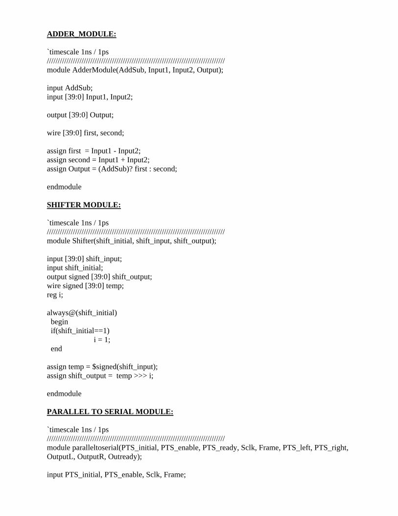
ADDER_MODULE:
`timescale 1ns / 1ps
//////////////////////////////////////////////////////////////////////////////////
module AdderModule(AddSub, Input1, Input2, Output);
input AddSub;
input [39:0] Input1, Input2;
output [39:0] Output;
wire [39:0] first, second;
assign first = Input1 - Input2;
assign second = Input1 + Input2;
assign Output = (AddSub)? first : second;
endmodule
SHIFTER MODULE:
`timescale 1ns / 1ps
//////////////////////////////////////////////////////////////////////////////////
module Shifter(shift_initial, shift_input, shift_output);
input [39:0] shift_input;
input shift_initial;
output signed [39:0] shift_output;
wire signed [39:0] temp;
reg i;
always@(shift_initial)
begin
if(shift_initial==1)
i = 1;
end
assign temp = $signed(shift_input);
assign shift_output = temp >>> i;
endmodule
PARALLEL TO SERIAL MODULE:
`timescale 1ns / 1ps
//////////////////////////////////////////////////////////////////////////////////
module paralleltoserial(PTS_initial, PTS_enable, PTS_ready, Sclk, Frame, PTS_left, PTS_right,
OutputL, OutputR, Outready);
input PTS_initial, PTS_enable, Sclk, Frame;
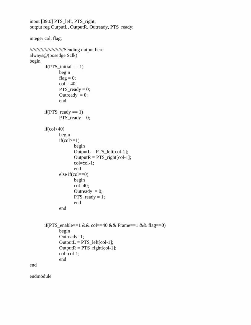
input [39:0] PTS_left, PTS_right;
output reg OutputL, OutputR, Outready, PTS_ready;
integer col, flag;
/////////////////////////Sending output here
always@(posedge Sclk)
begin
if(PTS_initial == 1)
begin
flag = 0;
col = 40;
PTS_ready = 0;
Outready = 0;
end
if(PTS_ready == 1)
PTS_ready = 0;
if(col<40)
begin
if(col>=1)
begin
OutputL = PTS_left[col-1];
OutputR = PTS_right[col-1];
col=col-1;
end
else if(col==0)
begin
col=40;
Outready = 0;
PTS_ready = 1;
end
end
if(PTS_enable==1 && col==40 && Frame==1 && flag==0)
begin
Outready=1;
OutputL = PTS_left[col-1];
OutputR = PTS_right[col-1];
col=col-1;
end
end
endmodule
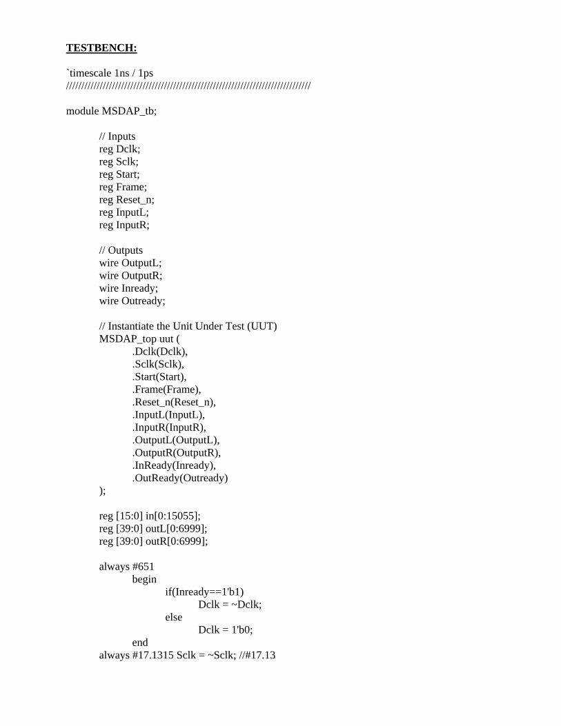
TESTBENCH:
`timescale 1ns / 1ps
////////////////////////////////////////////////////////////////////////////////
module MSDAP_tb;
// Inputs
reg Dclk;
reg Sclk;
reg Start;
reg Frame;
reg Reset_n;
reg InputL;
reg InputR;
// Outputs
wire OutputL;
wire OutputR;
wire Inready;
wire Outready;
// Instantiate the Unit Under Test (UUT)
MSDAP_top uut (
.Dclk(Dclk),
.Sclk(Sclk),
.Start(Start),
.Frame(Frame),
.Reset_n(Reset_n),
.InputL(InputL),
.InputR(InputR),
.OutputL(OutputL),
.OutputR(OutputR),
.InReady(Inready),
.OutReady(Outready)
);
reg [15:0] in[0:15055];
reg [39:0] outL[0:6999];
reg [39:0] outR[0:6999];
always #651
begin
if(Inready==1'b1)
Dclk = ~Dclk;
else
Dclk = 1'b0;
end
always #17.1315 Sclk = ~Sclk; //#17.13
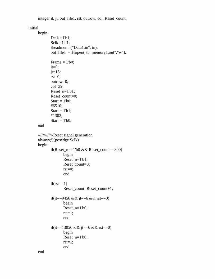
integer it, jt, out_file1, rst, outrow, col, Reset_count;
initial
begin
Dclk =1'b1;
Sclk =1'b1;
$readmemh("Data1.in", in);
out_file1 = $fopen("tb_memory1.out","w");
Frame = 1'b0;
it=0;
jt=15;
rst=0;
outrow=0;
col=39;
Reset_n=1'b1;
Reset_count=0;
Start = 1'b0;
#6510;
Start = 1'b1;
#1302;
Start = 1'b0;
end
/////////////Reset signal generation
always@(posedge Sclk)
begin
if(Reset_n==1'b0 && Reset_count==800)
begin
Reset_n=1'b1;
Reset_count=0;
rst=0;
end
if(rst==1)
Reset_count=Reset_count+1;
if(it==9456 && jt==6 && rst==0)
begin
Reset_n=1'b0;
rst=1;
end
if(it==13056 && jt==6 && rst==0)
begin
Reset_n=1'b0;
rst=1;
end
end
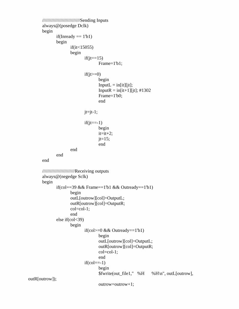
/////////////////////////////Sending Inputs
always@(posedge Dclk)
begin
if(Inready == 1'b1)
begin
if(it<15055)
begin
if(jt==15)
Frame=1'b1;
if(jt>=0)
begin
InputL = in[it][jt];
InputR = in[it+1][jt]; #1302
Frame=1'b0;
end
jt=jt-1;
if(jt==-1)
begin
it=it+2;
jt=15;
end
end
end
end
/////////////////////////Receiving outputs
always@(negedge Sclk)
begin
if(col==39 && Frame==1'b1 && Outready==1'b1)
begin
outL[outrow][col]=OutputL;
outR[outrow][col]=OutputR;
col=col-1;
end
else if(col<39)
begin
if(col>=0 && Outready==1'b1)
begin
outL[outrow][col]=OutputL;
outR[outrow][col]=OutputR;
col=col-1;
end
if(col==-1)
begin
$fwrite(out_file1," %H %H\n", outL[outrow],
outR[outrow]);
outrow=outrow+1;

col=39;
end
end
end
endmodule