Embed Size (px)
Citation preview
Hannes Ramon
ApplicationsFifth Generation (5G) Mobile Networks and AttocellDesign of a Broadband Signal Generation Platform for
Academic year 2014-2015Faculty of Engineering and ArchitectureChairman: Prof. dr. ir. Daniël De ZutterDepartment of Information Technology
Master of Science in Electrical EngineeringMaster's dissertation submitted in order to obtain the academic degree of
Counsellor: Haolin LiSupervisors: Dr. ir. Guy Torfs, Prof. dr. ir. Johan Bauwelinck

Preface
This master thesis has been a real learning school where the complete design cycle for RF design has
been undertaken. The design of a mixed signal RF front-end comes with many at first unexplainable and
parasitic effects, which requires out of the box thinking and in most of the cases experience in the matter
at hand. I want to thank my supervisors dr. ir. Guy Torfs and prof. dr. ir. Johan Bauwelinck first of all for
making it possible for me to execute this thesis, but also for providing support with their experience and
know-how in mixed signal RF design. The help of my counsellor ir. Haolin Li and other members of the
INTEC Design group, such as ir. Timothy De Keulenaer and ir. Arno Vyncke, was also much appreciated.
Designing a complex system requires a lot of testing before actually designing the final system. The
fabrication of these testing PCBs was not possible without the PCB milling machine of ing. Jan Gillis
and I want to thank him for taking his time and fabricating my boards. He also double checked my PCB
layout of the design for possible flaws and provided valuable insight in the PCB design flow.
Next I want to thank the department INTEC Design for putting their tools and measuring equipment at
my disposal.
During the complete year, talking to my friends and colleagues about the thesis was sometimes a real
relief. This thank you goes to some friends to whom I spoke daily about this thesis: Jelle Bailleul, Laurens
Bogaert, Gilles Bonne, Matthias Dewilde, Joris Lambrecht, Bob Mertens, Stef Vandermeeren, Zeger Van
de Vannet and Johannes Van Wonterghem.
Last but not least I also want to thank my family for their support and endless listening to me while
explaining my thoughts.
Hannes Ramon, May 2015
i

Permission to consult
The author gives permission to make this master dissertation available for consultation and to copy parts
of this master dissertation for personal use. In the case of any other use, the copyright terms have to be
respected, in particular with regard to the obligation to state expressly the source when quoting results
from this master dissertation.
Hannes Ramon, May 2015
ii

Design of a Broadband Signal Generation Platform for FifthGeneration (5G) Mobile Networks and Attocell Applications
by
Hannes Ramon
Master’s dissertation submitted in order to obtain the academic degree of
Master of Science in Electrical Engineering
Academic Year 2014-2015
Supervisors: Dr. ir. Guy Torfs, Prof. dr. ir. Johan Bauwelinck
Counselor: Haolin Li
Department of Information Technology
Chairmain: Prof. dr. ir. Daniel De Zutter
Faculty of Engineering and Architecture
Universiteit Gent
Abstract
With the rise of 5G mobile networks and attocell applications, the need for higher bandwidth signal
generation platforms ever increases. Current software defined radios only offer a couple of 10 MHz RF
bandwidth, while for these new applications hundreds of MHz would be necessary. In this master thesis,
a broadband (500 MHz) signal generation platform is developed further enable research in the 5G and
attocell domain. This platform can be divided into two main parts: a digital design with a powerful
FPGA followed by a mixed signal RF front-end. The mixed signal RF front-end consists of a powerful
high speed DAC, followed by an I/Q modulator which mixes to 5.5 GHz. The required low jitter clocks
and local oscillator are generated on the board. With respect to the digital part on the FPGA, a 5/6
resample filter is designed for convenient pulse shaping and predistortion filtering.
Keywords
Signal generation, FPGA, mixed-signal, RF, digital filter, 5G

Design of a Broadband Signal Generation Platformfor Fifth Generation (5G) Mobile Networks and
Attocell ApplicationsHannes Ramon
Supervisor(s): Dr. ir. Guy Torfs, prof. dr. ir. Johan Bauwelinck
Abstract—With the rise of 5G mobile networks and attocell applications,the need for higher bandwidth signal generation platforms ever increases.Current software defined radios only offer a couple of 10 MHz RF band-width, while for these new applications hundreds of MHz would be neces-sary. In this master thesis, a broadband (500 MHz) signal generation plat-form is developed further enable research in the 5G and attocell domain.This platform can be divided into two main parts: a digital design with apowerful FPGA followed by a mixed signal RF front-end. The mixed signalRF front-end consists of a powerful high speed DAC, followed by an I/Qmodulator which mixes to 5.5 GHz. The required low jitter clocks and lo-cal oscillator are generated on the board. With respect to the digital parton the FPGA, a 5/6 resample filter is designed for convenient pulse shapingand predistortion filtering.
Keywords—Signal generation, FPGA, mixed-signal, RF, digital filter, 5G
I. INTRODUCTION
NEW wireless communication systems require a muchhigher bandwidth due to the higher bitrate needed. Cur-
rent software defined radios only provide a couple of 10 MHz,but in order to deliver Gb/s wireless links to the users, a band-width of a factor 10 higher (in the order of 100 MHz) should beneeded. To enable research in this domain, a broadband signalgeneration platform around a powerful Kintex-7 FPGA is de-signed. It consists of two parts: a digital design on the FPGAand an analog front-end. This platform was specified to have a500 MHz RF bandwidth and an output frequency range of 5 to6 GHz.
II. DESIGN OF THE ANALOG FRONT-END
A. System architecture
The analog front-end consists of a DAC (Digital-to-Analogconverter), anti-imaging filters, an I/Q modulator and a RF am-plifier. The common clock is provided by a clock manager andthe LO (local oscillator) is generated by a synthesizer. Fig. 1shows a block diagram of the system architecture.
FPGA DAC
I
Q
I
Q
I
Q+
Clock generator Synthesizer
G
Fig. 1. System architecture
The DAC (AD9122) receives the digital signals I and Q sam-pled at 600 MHz and performs a digital to analog conversioncreating two analog signals I and Q that are filtered to removethe images introduced by the conversion. The analog filter is a
5th order low pass Chebychev-I (ε = 0.5 dB) (differential) filterwith cut-off frequency of 250 MHz. The filters directly connectto the I/Q modulator (LTC5588) for upconversion to 5.5 GHz.This LO is generated by the synthesizer (LTC6948-4) which re-ceives the PLL reference from the clock generator (AD9516-4).In addition, the clock generator also provides the 600 MHz DACand FPGA clock. Both the synthesizer and clock generator needto have a low phase noise output to minimize distortion.
B. Layout
Mixed signal PCB design requires careful routing and place-ment of the components. Fig. 2 shows a schematic representa-tion of the component placement and the most important con-nections on the PCB. The digital components (clock and DAC)are on the left, while the other analog components are placedon the right side of the board to minimize the interference be-tween the noisy digital signals and the sensitive analog signalsand components.
clock
DAC
synthesizer
I/Q mod.
FM
C c
on
ne
cto
r
RF out
Q-filter
I-filter
16 bit LVDS
FPGA clk
Clk outClk in
RF amplifier
Fig. 2. Schematic representation of the component placement
III. DESIGN OF DIGITAL RESAMPLING FIR FILTER
A. Introduction
The 500 MHz RF BW limits the symbol rate to 500 Mbaud,but the clock speed of the DAC is 600 MHz to enable a 1.1 over-sampling ratio. To convert the 500 MSPS (pulseshaped sym-bols) to 600 MSPS for digital-to-analog conversion a generaldigital resample filter with factor 1.1 is designed.
B. Topology
Traditional resampling is performed by upsampling to thelowest common multiple of both symbol rates, which is 3 GHzin this case. This 3 GHz signal is downsampled to 600 MHz.

The FPGA cannot handle the 3 GHz signal and by observingthat most of the upsampling operations actually are zero oper-ations, the upsampling is split into 6 parallel lower rate (500MHz) filters (filter 1 to 6) [1]. By performing a parallel to serialconversion on these 6 filters, the 3 GHz signal is reconstructed.When decimating directly on these 6 parallel outputs, only onefilter is active at each clock cycle and a multiplier reduction of6 can be performed when reusing the multipliers and adders. Tosolve timing problems with the fast 600 MHz clock, the filteris split into 2 Filter streams (indicated with capital F), Filter 1(contains filter 1, filter 5 and 3) and Filter 2 (contains filter 6,filter 4 and filter 2). After performing a parallel to serial con-version of the two Filters, the 600 MHz resampled signal is re-constructed. Fig. 3 shows the resample filter topology with theclock domains.
filter 1, filter 5, filter 3
filter 6, filter 4, filter 2
switching
block
Filter 1
Filter 2
500 MHz 600 MHz 300 MHz 600 MHz
P/S
Fig. 3. The factor 1.1 resample FIR filter topology
IV. RESULTS
A. Clock generation phase noise
Fig. 4 shows the phase noise measurement of the 50 MHzgenerated synthesizer reference. The phase noise for this signalis θrms = 0.0920 or equivalently the timing jitter is 5.11 psrms (integrated from 100 Hz to 1 MHz) [2].
102
103
104
105
106
−140
−130
−120
−110
−100
−90
−80
Frequency offset [Hz]
Pha
se n
oise
[dB
c/H
z]
Fig. 4. Measurement of the phase noise of the 50 MHz generated by the clockgenerator created synthesizer reference with a PLL loop BW of 100 kHz
B. Synthesizer phase noise
Fig. 4 shows the phase noise measurement of the 5.5 GHzgenerated LO. The phase noise for this signal is θrms = 4 orequivalently the timing jitter is 2.03 ps rms (integrated from 100Hz to 1 MHz) [2].
C. Full system
The full transmitter has been tested with and without the RFamplifier. Without the amplifier the output power equals -14dBm (Fig. 6) while with the RF amplifier this is equal to -2
102
103
104
105
106
−130
−120
−110
−100
−90
−80
−70
−60
−50
Frequency offset [Hz]
Pha
se n
oise
[dB
c/H
z]
Fig. 5. Measured phase noise of the 5.5 GHz LO generated by the synthesizerwith a PLL loop BW of 10 kHz
dBm (Fig. 7). The LO feedthrough is 30 dB suppressed withrespect to the wanted signal. Due to a biasing problem with theRF amplifier, some BW is lost into the amplifier.
5.44 5.46 5.48 5.5 5.52 5.54 5.56
x 109
110
100
90
80
70
60
50
40
30
20
10
f [Hz]
Po
we
r [d
Bm
]
-14 dBm-14 dBm
Fig. 6. Measured output spectrum of the I/Q modulator when I and Q are asine wave of 17 MHz generated by the DAC and a LO frequency of 5.5 GHzgenerated by the synthesizer (without RF amplifier)
5.45 5.46 5.47 5.48 5.49 5.5 5.51 5.52 5.53 5.54 5.55
x 109
100
90
80
70
60
50
40
30
20
10
0
f [Hz]
Po
we
r [d
Bm
]
-2.16 dBm -3.14 dBm
Fig. 7. Measured output spectrum of the I/Q modulator when I and Q are asine wave of 17 MHz generated by the DAC and a LO frequency of 5.5 GHzgenerated by the synthesizer (with RF amplifier)
V. CONCLUSIONS
A broadband signal generation platform was developed. TheRF bandwidth is when bypassing the RF amplifier larger than500 MHz, but with the RF amplifier (due to a biasing problem)this is greatly reduced.
REFERENCES
[1] Willim D. Richard, “Efficient parallel real-time upsampling with xilinxfpgas,” XPlanation: FPGA 101, 2014.
[2] Walt Kester, “Converting oscillator phase noise to time jitter,” AnalogDevices Tutorial MT-008.

Contents
1 Introduction 1
2 System Modeling 3
2.1 Introduction to digital communication . . . . . . . . . . . . . . . . . . . . . . . . . . . . . 3
2.1.1 Simple digital communication system . . . . . . . . . . . . . . . . . . . . . . . . . 3
2.1.2 Upsampling and pulse shaping . . . . . . . . . . . . . . . . . . . . . . . . . . . . . 5
2.1.3 Non ideal transmitter, receiver and channel . . . . . . . . . . . . . . . . . . . . . . 7
2.2 Proposed block diagram . . . . . . . . . . . . . . . . . . . . . . . . . . . . . . . . . . . . . 8
2.3 Clocking, frequency synthesis and phase noise . . . . . . . . . . . . . . . . . . . . . . . . . 8
2.3.1 Phase noise . . . . . . . . . . . . . . . . . . . . . . . . . . . . . . . . . . . . . . . . 9
2.3.2 Voltage controlled oscillator . . . . . . . . . . . . . . . . . . . . . . . . . . . . . . . 11
2.3.3 Phase locked loop and frequency synthesis . . . . . . . . . . . . . . . . . . . . . . . 12
2.4 Digital-to-analog conversion . . . . . . . . . . . . . . . . . . . . . . . . . . . . . . . . . . . 17
2.4.1 Noise and effective number of bits . . . . . . . . . . . . . . . . . . . . . . . . . . . 18
2.4.2 Sinc correction . . . . . . . . . . . . . . . . . . . . . . . . . . . . . . . . . . . . . . 19
2.4.3 Anti-imaging filter . . . . . . . . . . . . . . . . . . . . . . . . . . . . . . . . . . . . 21
2.5 I/Q modulation . . . . . . . . . . . . . . . . . . . . . . . . . . . . . . . . . . . . . . . . . . 21
2.5.1 Local oscillator phase noise . . . . . . . . . . . . . . . . . . . . . . . . . . . . . . . 23
2.5.2 Carrier leakage . . . . . . . . . . . . . . . . . . . . . . . . . . . . . . . . . . . . . . 24
2.5.3 I and Q imbalance . . . . . . . . . . . . . . . . . . . . . . . . . . . . . . . . . . . . 25
3 Component Selection 26
3.1 DAC . . . . . . . . . . . . . . . . . . . . . . . . . . . . . . . . . . . . . . . . . . . . . . . . 26
3.2 Clock distribution . . . . . . . . . . . . . . . . . . . . . . . . . . . . . . . . . . . . . . . . 29
3.3 Synthesizer . . . . . . . . . . . . . . . . . . . . . . . . . . . . . . . . . . . . . . . . . . . . 29
3.4 I/Q modulator . . . . . . . . . . . . . . . . . . . . . . . . . . . . . . . . . . . . . . . . . . 29
3.5 RF amplifier . . . . . . . . . . . . . . . . . . . . . . . . . . . . . . . . . . . . . . . . . . . 31
vi

CONTENTS vii
4 Printed Circuit Board Design 34
4.1 Board stackup . . . . . . . . . . . . . . . . . . . . . . . . . . . . . . . . . . . . . . . . . . 34
4.1.1 4-layer board . . . . . . . . . . . . . . . . . . . . . . . . . . . . . . . . . . . . . . . 34
4.1.2 6-layer board . . . . . . . . . . . . . . . . . . . . . . . . . . . . . . . . . . . . . . . 35
4.2 50 Ω single ended and 100 Ω differential traces . . . . . . . . . . . . . . . . . . . . . . . . 36
4.2.1 50 Ω single ended trace . . . . . . . . . . . . . . . . . . . . . . . . . . . . . . . . . 36
4.2.2 100 Ω differential traces . . . . . . . . . . . . . . . . . . . . . . . . . . . . . . . . . 39
4.3 Connection standards between the components . . . . . . . . . . . . . . . . . . . . . . . . 41
4.3.1 FPGA to DAC (Digital) . . . . . . . . . . . . . . . . . . . . . . . . . . . . . . . . . 41
4.3.2 FPGA to clock distribution . . . . . . . . . . . . . . . . . . . . . . . . . . . . . . . 44
4.3.3 Clock distribution to DAC with LVPECL (Digital) . . . . . . . . . . . . . . . . . . 45
4.3.4 DAC to I/Q modulator (Analog) . . . . . . . . . . . . . . . . . . . . . . . . . . . . 45
4.4 Schematics . . . . . . . . . . . . . . . . . . . . . . . . . . . . . . . . . . . . . . . . . . . . 51
4.4.1 DAC . . . . . . . . . . . . . . . . . . . . . . . . . . . . . . . . . . . . . . . . . . . . 51
4.4.2 Clock distribution . . . . . . . . . . . . . . . . . . . . . . . . . . . . . . . . . . . . 51
4.4.3 Synthesizer . . . . . . . . . . . . . . . . . . . . . . . . . . . . . . . . . . . . . . . . 51
4.4.4 I/Q modulator . . . . . . . . . . . . . . . . . . . . . . . . . . . . . . . . . . . . . . 54
4.4.5 RF amplifier . . . . . . . . . . . . . . . . . . . . . . . . . . . . . . . . . . . . . . . 54
4.5 Component placement . . . . . . . . . . . . . . . . . . . . . . . . . . . . . . . . . . . . . . 54
4.6 Off-board connections . . . . . . . . . . . . . . . . . . . . . . . . . . . . . . . . . . . . . . 56
4.7 Layout . . . . . . . . . . . . . . . . . . . . . . . . . . . . . . . . . . . . . . . . . . . . . . . 56
4.8 Calculation of Noise Figure (NF) . . . . . . . . . . . . . . . . . . . . . . . . . . . . . . . . 56
5 Configuring the Components 58
5.1 Design of the SPI block . . . . . . . . . . . . . . . . . . . . . . . . . . . . . . . . . . . . . 58
5.2 Configuring the board . . . . . . . . . . . . . . . . . . . . . . . . . . . . . . . . . . . . . . 62
5.3 FPGA constraints . . . . . . . . . . . . . . . . . . . . . . . . . . . . . . . . . . . . . . . . 64
6 Compensation and Pulse Shaping Filter 65
6.1 Normal 500 MHz FIR filter . . . . . . . . . . . . . . . . . . . . . . . . . . . . . . . . . . . 65
6.2 Resampling Finite Impulse Response (FIR) filter . . . . . . . . . . . . . . . . . . . . . . . 66
6.3 Clock Domain Crossing . . . . . . . . . . . . . . . . . . . . . . . . . . . . . . . . . . . . . 69
6.3.1 Two flip-flop synchronizer . . . . . . . . . . . . . . . . . . . . . . . . . . . . . . . . 69
6.3.2 Closed loop handshake synchronizers . . . . . . . . . . . . . . . . . . . . . . . . . . 70
6.3.3 First In First Out buffers . . . . . . . . . . . . . . . . . . . . . . . . . . . . . . . . 70
6.4 Resample filter optimizations . . . . . . . . . . . . . . . . . . . . . . . . . . . . . . . . . . 72
6.4.1 Multiplier reduction . . . . . . . . . . . . . . . . . . . . . . . . . . . . . . . . . . . 72

CONTENTS viii
6.4.2 Fully pipelined cascaded 500 MHz to 600 MHz resample FIR filter . . . . . . . . . 73
6.4.3 Split binary tree adder 500 MHz to 600 MHz resample FIR filter . . . . . . . . . . 75
7 Measurements 79
7.1 Testing the clock distribution . . . . . . . . . . . . . . . . . . . . . . . . . . . . . . . . . . 79
7.2 Testing the digital-to-analog convertor (DAC) and anti-imaging filter . . . . . . . . . . . . 80
7.2.1 FPGA-DAC interface . . . . . . . . . . . . . . . . . . . . . . . . . . . . . . . . . . 80
7.2.2 Signal distortion . . . . . . . . . . . . . . . . . . . . . . . . . . . . . . . . . . . . . 82
7.2.3 DAC jitter . . . . . . . . . . . . . . . . . . . . . . . . . . . . . . . . . . . . . . . . 83
7.2.4 Filter bandwidth . . . . . . . . . . . . . . . . . . . . . . . . . . . . . . . . . . . . . 84
7.3 Testing the synthesizer . . . . . . . . . . . . . . . . . . . . . . . . . . . . . . . . . . . . . . 86
7.4 Testing the I/Q modulator . . . . . . . . . . . . . . . . . . . . . . . . . . . . . . . . . . . 86
7.5 Full system with Radio Frequency (RF) amplifier . . . . . . . . . . . . . . . . . . . . . . . 87
8 Conclusions 91
8.1 Results . . . . . . . . . . . . . . . . . . . . . . . . . . . . . . . . . . . . . . . . . . . . . . . 91
8.2 Future work . . . . . . . . . . . . . . . . . . . . . . . . . . . . . . . . . . . . . . . . . . . . 92
Bibliography 94
A Schematics 96
B PCB Layout 100
C Hardware Description Languages and FPGA Design Flow 104
C.1 Hardware description language . . . . . . . . . . . . . . . . . . . . . . . . . . . . . . . . . 104
C.1.1 Combinatorial logic and always blocks . . . . . . . . . . . . . . . . . . . . . . . . . 104
C.1.2 Flip-flop’s and events . . . . . . . . . . . . . . . . . . . . . . . . . . . . . . . . . . 105
C.1.3 Finite state machine . . . . . . . . . . . . . . . . . . . . . . . . . . . . . . . . . . . 106
C.1.4 Avoiding latches . . . . . . . . . . . . . . . . . . . . . . . . . . . . . . . . . . . . . 108
C.2 HDL Synthesis . . . . . . . . . . . . . . . . . . . . . . . . . . . . . . . . . . . . . . . . . . 109
C.2.1 FPGA structure and implementation . . . . . . . . . . . . . . . . . . . . . . . . . . 109
C.2.2 Timing issues and constraints . . . . . . . . . . . . . . . . . . . . . . . . . . . . . . 109
D Constraint File for the FPGA 111

List of Figures
2.1 Difference 4-QAM and 4-PAM . . . . . . . . . . . . . . . . . . . . . . . . . . . . . . . . . 4
2.2 A simple block diagram of a digital communication system . . . . . . . . . . . . . . . . . 4
2.3 The spectrum of psquare with Ns = 10 and fS = 1 Mbaud . . . . . . . . . . . . . . . . . . 6
2.4 The Raised-cosine filter for different roll-off factros β (T is the symbolperiod) [20] . . . . . 6
2.5 The Raised-cosine impulse response for different roll-off factros β (T is the symbolperiod)
[20] . . . . . . . . . . . . . . . . . . . . . . . . . . . . . . . . . . . . . . . . . . . . . . . . . 7
2.6 Pulse shaping block diagram with p(k) the transmit pulse . . . . . . . . . . . . . . . . . . 7
2.7 Pulse removing block diagram with p∗(−k) the matched receiver filter to the transmit
pulse or transmit filter . . . . . . . . . . . . . . . . . . . . . . . . . . . . . . . . . . . . . . 7
2.8 Proposed block diagram . . . . . . . . . . . . . . . . . . . . . . . . . . . . . . . . . . . . . 8
2.9 Spectrum of s(t) with φpn(t) = m sin(2πfpnt) (fc = 1 MHz, fpn = 100 kHz, m = 0.03) . . 10
2.10 Typical phase noise power spectral density of a VCO . . . . . . . . . . . . . . . . . . . . . 12
2.11 Spectrum of a simulated oscillator at f = 1 MHz with phase noise floor at -200 dB and
fcorner = 100 KHz . . . . . . . . . . . . . . . . . . . . . . . . . . . . . . . . . . . . . . . . 13
2.12 Spectrum of a simulated oscillator at f = 1 MHz with phase noise floor at -200 dB and
fcorner = 1 MHz . . . . . . . . . . . . . . . . . . . . . . . . . . . . . . . . . . . . . . . . . 13
2.13 Simple PLL block diagram . . . . . . . . . . . . . . . . . . . . . . . . . . . . . . . . . . . . 14
2.14 Complexer PLL block diagram with PFD and CP . . . . . . . . . . . . . . . . . . . . . . 14
2.15 Possible implementation of the Phase Frequency Detector (PFD) with flip-flops [3] . . . . 15
2.16 A PLL Charge Pump (CP) . . . . . . . . . . . . . . . . . . . . . . . . . . . . . . . . . . . 15
2.17 PLL phase block diagram . . . . . . . . . . . . . . . . . . . . . . . . . . . . . . . . . . . . 15
2.18 Example loop filter for a second order Phase Locked Loop (PLL) . . . . . . . . . . . . . . 17
2.19 Example loop filter for a third order PLL . . . . . . . . . . . . . . . . . . . . . . . . . . . 17
2.20 Inverse sinc correcting 10 taps FIR filter frequency response for fDAC = 600 MHz . . . . 20
2.21 Simulated spectrum of 500 Mbaud (fDAC =600 MHz) transmission on a 5.5 GHz carrier
(no sinc correction, no anti-imaging filter) . . . . . . . . . . . . . . . . . . . . . . . . . . . 20
ix

LIST OF FIGURES x
2.22 Simulated spectrum of 500 Mbaud (fDAC =600 MHz) transmission on a 5.5 GHz carrier
(sinc correction, no anti-imaging filter) . . . . . . . . . . . . . . . . . . . . . . . . . . . . . 21
2.23 Simulated spectrum of 500 Mbaud (fDAC =600 MHz) transmission on a 5.5 GHz carrier
(sinc correction, anti-imaging filter) . . . . . . . . . . . . . . . . . . . . . . . . . . . . . . . 22
2.24 I/Q modulator schematic . . . . . . . . . . . . . . . . . . . . . . . . . . . . . . . . . . . . 23
3.1 Block Diagram of AD9122 [1] . . . . . . . . . . . . . . . . . . . . . . . . . . . . . . . . . . 28
3.2 Block Diagram of AD9516-4 [2] . . . . . . . . . . . . . . . . . . . . . . . . . . . . . . . . . 30
3.3 Block Diagram of LTC6948-4 [13] . . . . . . . . . . . . . . . . . . . . . . . . . . . . . . . . 31
3.4 Block Diagram of LTC5588 [12] . . . . . . . . . . . . . . . . . . . . . . . . . . . . . . . . . 32
4.1 Trace definition for the 50 Ω traces on top and bottom plane . . . . . . . . . . . . . . . . 36
4.2 Simulated S11 of a 30 mm long and 620 µm wide trace on top or bottom layer . . . . . . 37
4.3 Simulated S21 of a 30 mm long and 620 µm wide trace on top or bottom layer . . . . . . 37
4.4 Trace definition for the 50 Ω traces on layer 3 and 4 . . . . . . . . . . . . . . . . . . . . . 38
4.5 Simulated S11 of a 30 mm long and 620 µm wide trace on top or bottom layer (with
soldermask) . . . . . . . . . . . . . . . . . . . . . . . . . . . . . . . . . . . . . . . . . . . . 38
4.6 Trace definition for the 100 Ω traces on top and bottom layer . . . . . . . . . . . . . . . . 39
4.7 Simulated differential S11 of a 30 mm long, 240 µm wide traces with 100 µm separation
on top or bottom layer . . . . . . . . . . . . . . . . . . . . . . . . . . . . . . . . . . . . . . 39
4.8 Trace definition for the 100 Ω traces on layer 3 and 4 . . . . . . . . . . . . . . . . . . . . . 40
4.9 Simulated differential S11 of a 30 mm long, 240 µm wide traces with 100 µm separation
on top or bottom layer (with soldermask) . . . . . . . . . . . . . . . . . . . . . . . . . . . 40
4.10 An Low Voltage Differential signalling (LVDS) driver and receiver . . . . . . . . . . . . . 42
4.11 The crosstalk between layer 3 and 4 simulation configuration for LVDS . . . . . . . . . . . 42
4.12 Simulated LVDS voltage over an 100 Ω load when sending 1.2 Gb/s (alternating 1 and 0)
for the setup in Figure 4.11 . . . . . . . . . . . . . . . . . . . . . . . . . . . . . . . . . . . 43
4.13 Simulated far-end crosstalk (on victim line) voltage over an 100 Ω load when sending 1.2
Gb/s (alternating 1 and 0) (on the attacker) for the setup in Figure 4.11 . . . . . . . . . . 43
4.14 FPGA Mezzanine Card (FMC) VITA 57.1 Low Pin Count (LPC) standard [25, Figure B-2] 44
4.15 Simplified Low Voltage Positive Emittor Coupled Lines (LVPECL) driver [8] . . . . . . . 45
4.16 A possible LVPECL connection . . . . . . . . . . . . . . . . . . . . . . . . . . . . . . . . . 46
4.17 Current to voltage conversion network N . . . . . . . . . . . . . . . . . . . . . . . . . . . . 46
4.18 Resistor current to voltage converter . . . . . . . . . . . . . . . . . . . . . . . . . . . . . . 47
4.19 Resistor current to voltage converter with peak voltage reduction . . . . . . . . . . . . . . 47
4.20 Single ended to differential filter conversion . . . . . . . . . . . . . . . . . . . . . . . . . . 49

LIST OF FIGURES xi
4.21 Simulated S21 of the 5th order 250 MHz Chebychev-I anti-aliasing filter with passband
ripple ε = 0.5 dB . . . . . . . . . . . . . . . . . . . . . . . . . . . . . . . . . . . . . . . . . 50
4.22 Simulated phase noise plot of the 50 MHz generated synthesizer reference (with an esti-
mated reference for the clock distribution PLL) . . . . . . . . . . . . . . . . . . . . . . . . 52
4.23 Simulated amplitude Bode plot for the synthesizer PLL with N = 110, O = R = 1 and
cut-off frequency 10 kHz . . . . . . . . . . . . . . . . . . . . . . . . . . . . . . . . . . . . . 53
4.24 Simulated phase noise plot of the 5.5 GHz Local Oscillator (LO) by the synthesizer (with
reference from Figure 4.22) . . . . . . . . . . . . . . . . . . . . . . . . . . . . . . . . . . . 53
4.25 Visualisation of component placement and most important interconnections . . . . . . . . 55
4.26 The off-board connections. . . . . . . . . . . . . . . . . . . . . . . . . . . . . . . . . . . . . 56
5.1 Typical Serial Peripheral Interface (SPI) configuration with 2 slaves . . . . . . . . . . . . 59
5.2 A SPI read operation: the master asks the content of register 0x70 (actual command is
0x71, but the last bit is a read bit) and receives as response 0x2. . . . . . . . . . . . . . . 59
5.3 The pinout of the designed SPI-master block . . . . . . . . . . . . . . . . . . . . . . . . . 60
5.4 Simplified SPI-master block diagram of Figure 5.3 . . . . . . . . . . . . . . . . . . . . . . 60
5.5 SPI master Finite State Machine (FSM) . . . . . . . . . . . . . . . . . . . . . . . . . . . . 62
5.6 SPI output driver with shift register (flip-flops are falling edge flip-flops) . . . . . . . . . . 62
5.7 SPI input driver with shift register (flip-flops are rising edge flip-flops) . . . . . . . . . . . 63
6.1 Normal 4 taps (Ns = 4) FIR filter with binary tree addition . . . . . . . . . . . . . . . . . 66
6.2 Normal 4 taps (Ns = 4) FIR filter with cascaded addition . . . . . . . . . . . . . . . . . . 66
6.3 Demonstration of the resampling process (Dotted lines at 600 Megasamples per second
(MSPS) are not part of the signal but only present to show the original signal before
downsampling) . . . . . . . . . . . . . . . . . . . . . . . . . . . . . . . . . . . . . . . . . . 67
6.4 Parallel stream upsampling filter for conversion from 500 MHz to 3 GHz . . . . . . . . . . 68
6.5 Single flip-flop synchronizer . . . . . . . . . . . . . . . . . . . . . . . . . . . . . . . . . . . 69
6.6 Two flip-flop synchronizer . . . . . . . . . . . . . . . . . . . . . . . . . . . . . . . . . . . . 70
6.7 An asynchronous First In First Out (FIFO) with empty and full generation [5] . . . . . . 72
6.8 A binary tree addition resample FIR filter (pipelined) . . . . . . . . . . . . . . . . . . . . 73
6.9 A pipelined cascaded addition FIR filter . . . . . . . . . . . . . . . . . . . . . . . . . . . . 73
6.10 A pipelined cascaded addition FIR filter with standard cells . . . . . . . . . . . . . . . . . 74
6.11 The complete standard cell with coefficient generation for the pipelined cascade adder FIR
filter . . . . . . . . . . . . . . . . . . . . . . . . . . . . . . . . . . . . . . . . . . . . . . . . 74
6.12 Resample FIR filter topology with two parallel lower rate filter streams . . . . . . . . . . 75
6.13 The shift-by-one-or-two shift register for the split resample FIR filter . . . . . . . . . . . . 76
6.14 The switching block from Figure 6.12 . . . . . . . . . . . . . . . . . . . . . . . . . . . . . . 76

LIST OF FIGURES xii
6.15 The full switching block from Figure 6.12 with FIFO routing . . . . . . . . . . . . . . . . 78
7.1 Measured (frequency domain) 50 MHz clock generated by the clock generator . . . . . . . 80
7.2 Measured (time domain) 50 MHz clock generated by the clock generator . . . . . . . . . . 80
7.3 Measured phase noise of the 50 MHz generated clock with the reference from the FPGA . 81
7.4 Measured phase noise of the 50 MHz generated clock with the reference from the signal
generator . . . . . . . . . . . . . . . . . . . . . . . . . . . . . . . . . . . . . . . . . . . . . 81
7.5 Measured waveform of one bit of the FPGA-DAC interface when transmitting 50 MHz
square wave on I and 0 on Q . . . . . . . . . . . . . . . . . . . . . . . . . . . . . . . . . . 82
7.6 Measured spectrum of a generated 200 MHz sine wave (Power at 200 MHz is -6 dBm) . . 83
7.7 Measured spectrum of a generated 17 MHz sine wave (Power at 17 MHz is -6 dBm) . . . 84
7.8 Measured spectrum of a three equal power tones at 50, 100 and 200 MHz (Power of
fundamental tones -14 dBm) . . . . . . . . . . . . . . . . . . . . . . . . . . . . . . . . . . 84
7.9 Measured phase noise of a generated 17 MHz sine (with FPGA clock as reference for clock
generation) . . . . . . . . . . . . . . . . . . . . . . . . . . . . . . . . . . . . . . . . . . . . 85
7.10 Measured anti-imaging filter by sending a chirping cosine with frequency up until 300 MHz 85
7.11 Measured spectrum of the LO generated by the synthesizer at 5.5 GHz . . . . . . . . . . . 86
7.12 Measured phase noise of the 5.5 GHz LO generated by the synthesizer with a PLL loop
bandwidth (BW) of 10 kHz (with the reference from signal generator for clock generation) 87
7.13 Measured output spectrum of the I/Q modulator when I and Q are a sine wave of 17
MHz generated by the DAC and an LO frequency of 5.5 GHz generated by the synthesizer
(without RF amplifier) . . . . . . . . . . . . . . . . . . . . . . . . . . . . . . . . . . . . . . 88
7.14 Measured output spectrum of the I/Q modulator when I and Q are a sine wave of 17 MHz
generated by the DAC and an LO frequency of 5.5 GHz generated by the synthesizer (with
RF amplifier) . . . . . . . . . . . . . . . . . . . . . . . . . . . . . . . . . . . . . . . . . . . 89
7.15 Measured output spectrum of the I/Q modulator when I and Q are a sine wave of 250
MHz generated by the DAC and an LO frequency of 5.5 GHz generated by the synthesizer
(with RF amplifier) . . . . . . . . . . . . . . . . . . . . . . . . . . . . . . . . . . . . . . . . 89
7.16 Measured output spectrum of the I/Q modulator when I and Q are a sine wave of 200
MHz generated by the DAC and an LO frequency of 5.5 GHz generated by the synthesizer
(with RF amplifier) . . . . . . . . . . . . . . . . . . . . . . . . . . . . . . . . . . . . . . . . 90
7.17 Measured output spectrum of the I/Q modulator when I and Q are a sine wave of 17 MHz
generated by the DAC and LO frequency 5.315 GHz generated by the synthesizer (with
RF amplifier) . . . . . . . . . . . . . . . . . . . . . . . . . . . . . . . . . . . . . . . . . . . 90
A.1 Schematic of the DAC (AD9122) . . . . . . . . . . . . . . . . . . . . . . . . . . . . . . . . 96
A.2 Schematic of the clock (AD9516-4) . . . . . . . . . . . . . . . . . . . . . . . . . . . . . . . 97

LIST OF FIGURES xiii
A.3 Schematic of the synthesizer (LTC6948-4) . . . . . . . . . . . . . . . . . . . . . . . . . . . 98
A.4 Schematic of the I/Q modulator (LTC5588) . . . . . . . . . . . . . . . . . . . . . . . . . . 99
A.5 Schematic of the RF amplifier (GVA-83+) . . . . . . . . . . . . . . . . . . . . . . . . . . . 99
B.1 Layout layer 1 . . . . . . . . . . . . . . . . . . . . . . . . . . . . . . . . . . . . . . . . . . . 100
B.2 Layout layer 2 . . . . . . . . . . . . . . . . . . . . . . . . . . . . . . . . . . . . . . . . . . . 101
B.3 Layout layer 3 . . . . . . . . . . . . . . . . . . . . . . . . . . . . . . . . . . . . . . . . . . . 101
B.4 Layout layer 4 . . . . . . . . . . . . . . . . . . . . . . . . . . . . . . . . . . . . . . . . . . . 102
B.5 Layout layer 5 . . . . . . . . . . . . . . . . . . . . . . . . . . . . . . . . . . . . . . . . . . . 102
B.6 Layout layer 6 . . . . . . . . . . . . . . . . . . . . . . . . . . . . . . . . . . . . . . . . . . . 103
B.7 A photograph of the soldered PCB . . . . . . . . . . . . . . . . . . . . . . . . . . . . . . . 103
C.1 Equivalent combinatorial circuit of Code C.1 . . . . . . . . . . . . . . . . . . . . . . . . . 105
C.2 Equivalent circuit of Code C.3 . . . . . . . . . . . . . . . . . . . . . . . . . . . . . . . . . 107
C.3 Equivalent circuit of Code C.4 . . . . . . . . . . . . . . . . . . . . . . . . . . . . . . . . . 107

List of Tables
3.1 Some specifications of the AD9122 DAC [1] . . . . . . . . . . . . . . . . . . . . . . . . . . 27
3.2 Some specifications of the AD9516-4 clock distribution [2] . . . . . . . . . . . . . . . . . . 29
3.3 Some specifications of the LTC6948-4 synthesiser [13] . . . . . . . . . . . . . . . . . . . . . 30
3.4 Some specifications of the LTC5588 I/Q modulator [12] . . . . . . . . . . . . . . . . . . . 32
3.5 Some specifications of the GVA-83+ RF amplifier [14] . . . . . . . . . . . . . . . . . . . . 33
4.1 Layer stackup for 6-layer board . . . . . . . . . . . . . . . . . . . . . . . . . . . . . . . . . 35
4.2 Custom layer buildup for impedance control (copper clearance and angular ring 100 µm) . 36
4.3 Fifth order Chebychev-I (cut-off frequency at 250 MHz) trade-off between passband ripple
and stopband attenuation . . . . . . . . . . . . . . . . . . . . . . . . . . . . . . . . . . . . 49
4.4 Overview of the provided connections in and out of the board. . . . . . . . . . . . . . . . 57
5.1 SPI block pinout . . . . . . . . . . . . . . . . . . . . . . . . . . . . . . . . . . . . . . . . . 61
6.1 Order of taking the samples from each filter for directly decimation of the parallel streams
to 600 MHz . . . . . . . . . . . . . . . . . . . . . . . . . . . . . . . . . . . . . . . . . . . . 68
6.2 Functionality of the switching circuit when filtering a(k) = k + 1 with k starting from 0 . 77
7.1 Phase noise summary of the 50 MHz generated clock (integrated from 100 Hz to 1 MHz) . 82
xiv

List of Acronyms
BW bandwidth
CDC Clock Domain Crossing
CLB Configurable Logic Block
CP Charge Pump
DAC digital-to-analog convertor
DDR Double Data Rate
DSP Digital Signal Processing
ENOB Effective Number of Bits
FIFO First In First Out
FIR Finite Impulse Response
FMC FPGA Mezzanine Card
FSM Finite State Machine
HDL Hardware Description Language
LO Local Oscillator
LPC Low Pin Count
LVDS Low Voltage Differential signalling
LVPECL Low Voltage Positive Emittor Coupled Lines
LUT Lookup Table
MSPS Megasamples per second
xv

LIST OF ACRONYMS xvi
NCO numerically controlled oscillator
NF Noise Figure
PCB Printed Circuit Board
PFD Phase Frequency Detector
PLL Phase Locked Loop
SCLK Serial Clock
SDI Serial Data In
SDO Serial Data Out
SPI Serial Peripheral Interface
SNR Signal-to-Noise Ratio
SSB Single-Sideband
RAM Random-Access Memory
RF Radio Frequency
VCO Voltage Controlled Oscillator

Chapter 1
Introduction
Currently, the development of the 5th generation mobile networks is in progress and in addition investi-
gator are researching technology to provide wireless communication into very small cells, called attocells.
Both applications share the common need for very high data rates and hence, rely on very high-speed
electronics. In order to provide all the users Gb/s wireless capability, broadband signal generation plat-
forms are needed to devise and test new wireless concepts. Current commercial software defined radio
platforms are too limited in bandwidth for this research. They mostly only provide a couple of 10 MHz,
while new wireless communication networks start to utilize much higher bandwidths (order hundreds of
MHz) available in the mmWave range.
The main objective of this thesis is to design a reconfigurable broadband test platform around a pow-
erful FPGA. This test platform requires not only a powerful FPGA, but also a broadband analog/RF
front-end, which converts the digital signals from the FPGA to the analog domain. The analog front-end
requires a 500 MHz bandwidth and an RF output frequency in the GHz range which has been chosen for
testing purposes around the ISM band of 5.5 GHz.
Thesis structure
Chapter 2 gives the theoretical background about communication systems. Based on this background,
a block diagram will be composed. Each component in the block diagram is investigated for possible
problems and theoretical solutions will be proposed.
After the composition of the block diagram, Chapter 3 discusses the chosen components and their speci-
fications followed by Chapter 4 in which the Printed Circuit Board (PCB) design is discussed. Chapter
3 and 4 together form the design of the analog/RF front-end.
1

CHAPTER 1. INTRODUCTION 2
Chapter 5 and 6 continue with the digital part of the design and the FPGA implementation.
Finally, Chapter 7 handles the measurement results obtained from the platform. Chapter 8 finishes
this thesis with the results and conclusions.

Chapter 2
System Modeling
2.1 Introduction to digital communication
With the ever increasing need to send (digital) data faster and faster from one end of the world to
the other, digital communication becomes complexer and this comes with a higher demands on the
specifications for the systems generating and receiving the data. In order to be able to understand
what components are important for a signal generation platform for digital communication, some basic
components and design considerations are introduced.
2.1.1 Simple digital communication system
The simplest form of digital communication is to send the bits directly, either unmodulated or modulated
(on-off keying or Amplitude Shift Keying) on a channel carrier. This form of digital communication is
particularly useful if the bit rate of the data is well within the maximal channel bandwidth.
To transmit bit rates that are higher than the channel bandwidth, the bits are grouped and sent at the
same time. Each group of bits are called a data symbol. By grouping n bits, there are 2n possible
symbols, and therefore 2n different signal levels that can be transmitted. Actually, the transmission of
symbols is an extension of the direct transmission of bits. Take n = 1, then there are 2 signal levels to
transmit, either a 0 or a 1.
There are many possible ways to construct the 2n different symbols and we call each possibility a constella-
tion. Not all constellations are equally efficient, and hence most communication systems use standardized
constellation diagrams like M-QAM or Quadrature Amplitude Modulation with M symbols, M-PSK or
Phase Shift Keying with M symbols, . . . The discussion of the different constellation diagrams is beyond
the scope of this master thesis, but [16] discusses these constellations.
Most digital communication systems include an extra dimension, the imaginary axis, so the symbols be-
come complex valued. This is to reduce the effect of noise as the points are now divided over 2 orthogonal
3

CHAPTER 2. SYSTEM MODELING 4
axis and the distance between each point can be larger (Figure 2.1).
1+1j
1-1j-1-1j
-1+1jIm
Re
4-QAM
Im
Re
4-PAM
1-1
-0.5
0.5
Figure 2.1: Difference 4-QAM and 4-PAM
A digital transmitter first maps the bits to the constellation symbols and sends these symbols to the
DAC. From there on, the signals are in the analog domain upconverted to the desired frequency channel
using a LO. After the transmission over the channel, the receiver downconverts the signal to baseband
and samples the signal in the analog-to-digital converter. The receiver performs some digital filtering,
guesses the transmitted data symbols and finally demaps these symbols to get the received bits (Figure
2.2).
Mapper DACPulse shaping
filterNs
Pulse shaping
LO
ChannelBitstream
LO
ADCPulse filterNs
Pulse removing
DemapperBitstream
Transmitter
Receiver
Digital Analog
Figure 2.2: A simple block diagram of a digital communication system
The explanation of 2 blocks (pulse shaping and pulse removing) were deliberately left out of the expla-

CHAPTER 2. SYSTEM MODELING 5
nation in the previous paragraph. What these blocks do and why they are in the block diagram is the
subject of the next section (section 2.1.2).
The maximal symbol rate (unit of symbol rate is baud) is limited by the channel bandwidth. Since each
symbol actually stands for n bits, the net bit rate can drastically be increased by increasing the number
of bits per symbol (n). However, increasing n often means much harder requirements for the transmitter
and receiver in terms of noise and distortion.
2.1.2 Upsampling and pulse shaping
After the generation of the symbols, there are several possibilities to send these symbols to the DAC
for conversion to actual analog signals. The most obvious solution is to perform a zero order hold
interpolation. This means that we hold the symbol at the output of de DAC for the whole symbol period
duration.when defining the ratio between the symbol rate fS and the DAC sampling rate fs as Ns(number
of samples per symbol) (2.1), than zero order hold interpolation can be mathematically expressed as the
convolution between the vector obtained by placing Ns − 1 zeros between the symbols and the digital
square wave (2.2). The addition of zeros between the data symbols is called upsampling with a factor
Ns. The digital square wave acts as the interpolation filter after the upsampling.
Ns =fsfS
(2.1)
psquare(k) =
0 , k < 0
1 , 0 ≤ k < Ns
0 , k ≥ Ns
(2.2)
At first this seems a simple and good solution, however when looking at the frequency domain of the
signal after the zero order hold interpolation, the original spectrum of the symbols has been changed.
This is because psquare in the frequency domain is a sinc function which is not frequency flat in the
useful signal band. The sinc spectrum of psquare is also relatively broad and can cause interference
with other communication channels. Figure 2.3 shows the sinc spectrum of a psquare with Ns = 10 and
fS = 1 Mbaud. The sinc spectrum decays very slow to 0 and interference is almost unavoidable. When
transmitting at 1 Mbaud, the signal spectrum will be located between f = −0.5 MHz and f = 0.5 MHz.
Figure 2.3 shows that the spectrum of psquare is far from flat in that frequency region.
If a flat frequency response and a much smaller bandwidth is needed, we can start with a flat and narrow
filter from the frequency domain and perform an inverse Fourrier transform (inv FT). Due to the duality
of the FT, the inv FT of a rectangular filter is a sinc in time domain. There are many possibilities in
the frequency domain that fulfil the frequency flat and band limited requirements, but the raised-cosine
filter (G(f)) is commonly used in communication systems (Figure 2.4 and Figure 2.5).

CHAPTER 2. SYSTEM MODELING 6
−5 −4 −3 −2 −1 0 1 2 3 4 5
x 106
−90
−80
−70
−60
−50
−40
−30
−20
−10
0
f [Hz]
S(f
)/S
(0)
[dB
]
Figure 2.3: The spectrum of psquare with Ns = 10 and fS = 1 Mbaud
Figure 2.4: The Raised-cosine filter for different roll-off factros β (T is the symbolperiod) [20]
The process of changing the transmit pulse for the symbols to make the transmitted signals more band
limited is called pulse shaping. The filter is then naturally called the pulse shaping filter. On the transmit
side we can replace the pulse shaping block in Figure 2.2 by an upsampler with factor Ns and a pulse
shaping filter p(k) (Figure 2.6). On the receiving side, the pulse p(k) needs to be removed. This is done
by filtering with the matched filter p∗(−k) (p∗(k) is the complex conjugate of p(k)) and decimating the
sampled signal by a factor Ns (Figure 2.7). The reason why the receiver filter is p∗(−k) is beyond the
scope of this master thesis but can be read in e.g. [15]

CHAPTER 2. SYSTEM MODELING 7
Figure 2.5: The Raised-cosine impulse response for different roll-off factros β (T is the symbolperiod)
[20]
Ns p(k)
Figure 2.6: Pulse shaping block diagram with p(k) the transmit pulse
Ns p*(-k)
Figure 2.7: Pulse removing block diagram with p∗(−k) the matched receiver filter to the transmit pulse
or transmit filter
To avoid inter symbol interference (ISI), the convolution g(k) = p(k) ∗ p∗(−k) needs to be δ(k) after
decimation by Ns. This is true if g(k) is equal to the raised-cosine filter (Figure 2.5). There are also
other possibilities for g(k) who fulfil to the δ(k) condition. p(k) can be derived from G(f) according to
(2.3).
H(f) =√|G(f)| ←→ p(k) (2.3)
2.1.3 Non ideal transmitter, receiver and channel
In reality, the transmitter, nor the receiver and the transmission channel are ideal. In communication
systems, we still strive to a total filter g(k) equal to the raised-cosine filter. To accomplish this, commu-
nication systems need compensation for non-ideal transmitter, receiver and the channel. This can e.g.
be performed in the transmitter by a predistortion filter.

CHAPTER 2. SYSTEM MODELING 8
2.2 Proposed block diagram
Based on the simple digital communications model of the previous section, the block diagram in Figure
2.8 for the design of a transmitter is proposed.
FPGA DAC
I
Q
I
Q
I
Q+
Clock generator Synthesizer
G
Figure 2.8: Proposed block diagram
The FPGA generates the I and Q signals and sends them to the DAC for conversion to the analog
domain. The I and Q signals are defined in (2.4) with a(k) the kth symbol to be transmitted and p(k)
the root-raised-cosine pulse earlier defined.
I(k) =
∞∑l=−∞
Re[a(l)]p(k − lNs)
Q(k) =
∞∑l=−∞
Im[a(l)]p(k − lNs) (2.4)
This DAC is followed by an anti-imaging or reconstruction filter and a I/Q modulator or upconvertor to
mix the base band signal the specified frequency band. Afterwards a broadband amplifier provides the
necessary power at the output.
Furthermore, the clock generator synchronizes all the blocks and provides the synthesizer the needed
reference for the generation of the LO. A feature that is not visible on this block diagram is the possibility
to synchronize multiple transmitter systems to the same clock by providing a cascade reference clock for
the clock generator.
2.3 Clocking, frequency synthesis and phase noise
In digital communications and more general in digital systems, everything is synchronized to a common
clock. This clock is preferably generated by a single clock generator, so every subsystem has the same
clock and if the distribution is phase matched, the same clock phase. Some subsystems need a reference
clock to generate their own clock or oscillating signals. These subsystems often need a lower frequency
reference clock which is a divided version of the common clock. An example of such a subsystem is a
frequency synthesizer used for generating a LO for up or down conversion of the signals to other frequency

CHAPTER 2. SYSTEM MODELING 9
bands. Clock generators and more general electrical oscillators are not perfect and their performance is
determined by e.g. relative frequency offset, phase noise, . . . .
2.3.1 Phase noise
One of the most concerning technical aspects of an oscillator in frequency synthesis is phase noise. An
oscillator has a well defined amplitude which is controlled by the control loop at unity gain. Small
perturbations in amplitude are rejected by the oscillator. The phase of the oscillator on the other hand
is not constrained because any phase shifted oscillation running at the same frequency is a valid solution.
Perturbations in phase are hence not rejected and they introduce a permanent phase error. These changes
in phase cause local frequency changes of the oscillation frequency.
To explain the influences of phase noise, we start from a sine generating oscillator with frequency fc and
amplitude A:
s(t) = A sin(2πfct)
with a singe side band spectrum (SSB spectrum):
S(f) =A
2δ(f − fc)
Real oscillators show some slow frequency drift fc(t), however in communication systems, this slow
frequency drift at the transmitter is countered by good receiver equipment and we can easily assume
that the receiver knows fc(t) ≈ fc. Besides the slow frequency drift, there are also fast fluctuations in
frequency that cause a widening of the SSB spectrum. These fast fluctuations are random and we can
represent them as a random fluctuation in the phase of the oscillator output.
s(t) = A sin (2πfct+ φpn(t))
with φpn(t) the random phase fluctuations or phase noise. The noise spectral density of phase noise is
often expressed in dBc/Hz with dBc the unit for amplitude variation according to the SSB carrier power
A2/4 in our case. To see what happens in the frequency domain, we can see this as a phase modulated
signal modulated with φpn(t). To make the calculation easier, we take φpn(t) = m sin(2πfpnt) with m
the modulation index en fpn the modulation frequency. This can then later easily be generalized by a
taking a sum over all the frequency components of φpn(t).
The SSB power spectrum of s(t) = A sin (2πfct+m sin(2πfpnt)) is determined by Bessel functions (Figure
2.9) and when m is small, the higher order Bessel coefficients (>1) and sidebands can be neglected [3,
p.41].
The only significant sidebands generated by φpn(t) have magnitude m2/4 in power or m/2 in amplitude:

CHAPTER 2. SYSTEM MODELING 10
0 0.5 1 1.5 2 2.5 3 3.5 4 4.5 5
x 106
−350
−300
−250
−200
−150
−100
−50
0
f [Hz]
Pow
er [d
B]
Figure 2.9: Spectrum of s(t) with φpn(t) = m sin(2πfpnt) (fc = 1 MHz, fpn = 100 kHz, m = 0.03)
S(f) =A
2
[δ(f − fc) +
m
2δ(f − (fc − fpn)) +
m
2δ(f − (fc + fpn))
]The power at fc is normally also affected by the modulation, but in the approximation where m 1,
the Bessel coefficient belonging to fc is approximately 1. This modulation broadens the spectrum of
oscillator. The SSB noise spectrum of φpn(t) then becomes
m2
4δ(f − fpn) (2.5)
Phase noise is often expressed as jitter in the time domain. Integrating (2.5) gives the jitter in rad2 rms
[18] [10]
θjitter,rms[rad] =
√2
∫ ∞0
m2
4δ(f − fpn)df =
m√2
θjitter,rms gives an indication how much the phase of the oscillator changes due to the phase noise
present. If the mean value of the phase noise is 0, then θjitter,rms is equal to the variance of the phase
noise. However, a phase change is not always practical to use in the time domain, so we can transform
this θjitter,rms to tjitter,rms, an indication of the time shift due to phase noise.
tjitter,rms =θjitter,rms
2πfc
To illustrate these formulas, a 1 MHz signal is modulated with a sinusoidal phase noise with m = 0.01
and fpn = 10 kHz. m = 0.01 means that the phase noise has a peak variation of 0.1 kHz or 100 Hz.

CHAPTER 2. SYSTEM MODELING 11
Next, all the properties of the phase noise are calculated by using the above formulas
SSB power =0.012
4= −46 dBc/Hz
θjitter,rms = 7 · 10−3 rad = 0.405
tjitter,rms = 1.125 ns
A 100 Hz peak variation at 10 kHz offset from oscillation frequency fc = 1 MHz gives 1.125 ns rms jitter.
This is quite small compared to the period of 1 µs of fc but this is because only one phase noise frequency
is present. In real systems, the phase noise consists of a lot of frequencies. We can still follow the same
reasoning as above by using superposition
φpn =∑i
mi sin(2πfpn,it)
If we represent the SSB spectrum of this phase noise by Lpn(f), the calculation of θjitter,rms can be
generalized by
θjitter,rms =
√2
∫ ∞0
Lpn(f)df (2.6)
2.3.2 Voltage controlled oscillator
In communication and clock distribution systems, we often use a Voltage Controlled Oscillator (VCO).
A VCO is an oscillator with a variable oscillation frequency fc which is controlled by applying a voltage.
A simple model for a VCO is proposed in (2.7) with f the free running frequency when no voltage is
applied, v(t) the control voltage and Kp the sensitivity to the control voltage.
s(t) = A cos
(2πft+ 2πKp
∫ t
0
v(u)du
)(2.7)
To evaluate if (2.7) behaves as a VCO, we can take v(t) = c, a constant. s(t) becomes
s(t) = A cos
(2πft+ 2πKp
∫ t
0
c · du)
= A cos (2π(f +Kpc)t)
which shows that the oscillator frequency has changed from f to (f +Kpc).
Due to the frequency changing nature of the VCO, communication systems frequently use the VCO for
frequency modulation with v(t) the useful information. Any perturbation on v(t) due to e.g. noise also
contributes to phase and frequency changes of the VCO output, which inherently leads to phase noise.
This means that any noise present in v(t) automatically transforms to phase noise at the output of the
VCO.
The noise spectral density (Lpn(f)) of a VCO and in general oscillators depends on 1f3 , 1
f2 and 1f noise

CHAPTER 2. SYSTEM MODELING 12
until the noise floor is reached. However in most cases we can neglect the influence of 1f3 and 1
f2 noise
because they are only significant at very low frequency offset from the oscillation frequency. The noise
spectrum mostly is by the 1f corner frequency (fcorner) and the noise floor. The corner frequency is the
frequency where the noise floor becomes dominant over the 1f noise (Figure 2.10).
Noise floor
1/f3
1/f2
1/f
fcorner f [dB]
No
ise
po
we
r [d
B]
Figure 2.10: Typical phase noise power spectral density of a VCO
We can model the phase noise power spectrum density by generating white noise at the noise floor and
filtering this white noise with (2.8).
T (s) =1 + sτcornersτcorner
(2.8)
With τcorner = 12πfcorner
the time constant belonging to the corner frequency fcorner.
When we include this phase noise model into an oscillator running e.g. at 1 MHz we obtain Figures
2.11 and 2.12 respectively for a corner frequency of 100 kHz and 1 MHz. The noise floor is -200 dB. We
can easily read the corner frequency from these figures.
A VCO has a lower and an upper operation frequency which is called the tuning range of the VCO.
When using a VCO in a design, the tuning frequency can be an important parameter.
For frequency modulation, the VCO can be a practical tool, but if you want to create tunable single
frequency oscillation, this can be cumbersome with just a control voltage. The VCO frequency can drift
even when applying a constant control voltage. This is why we can place the VCO inside a loop (phase
locked loop) to control the output frequency and also keep the phase as steady as possible.
2.3.3 Phase locked loop and frequency synthesis
A Phase Locked Loop (PLL) is a complex control loop for locking the phase and frequency of a VCO
to the phase and frequency of a reference clock. A PLL computes the phase and frequency difference
between the reference clock and a frequency divided (N) version of the VCO output. The PLL filters

CHAPTER 2. SYSTEM MODELING 13
−5 −4 −3 −2 −1 0 1 2 3 4 5
x 106
−250
−200
−150
−100
−50
0
f [Hz]
Pow
er [d
B]
Figure 2.11: Spectrum of a simulated oscillator at f = 1 MHz with phase noise floor at -200 dB and
fcorner = 100 KHz
−5 −4 −3 −2 −1 0 1 2 3 4 5
x 106
−250
−200
−150
−100
−50
0
f [Hz]
Pow
er [d
B]
Figure 2.12: Spectrum of a simulated oscillator at f = 1 MHz with phase noise floor at -200 dB and
fcorner = 1 MHz
this phase and frequency difference with a low pass filter H(f) which produces the tuning voltage for the
VCO (Figure 2.13).
When the PLL locks, the phase of the VCO should be equal to the reference phase and fV CO = NO fref
with fref the reference frequency. By changing N , we can change the VCO output frequency and due to

CHAPTER 2. SYSTEM MODELING 14
H(s)
1N
1R
1O
VCOFrequency
difference
Figure 2.13: Simple PLL block diagram
the closed loop, this frequency should be stable for a given value of N . This makes a PLL particularly
useful for frequency synthesis and clock distribution. Frequency synthesis is the art of stepping through
the in frequency separated communication channels by changing the frequency of the LO with the fixed
frequency channel spacing. With a PLL, this is particularly simple by changing the reference divider,
loop divider and output divider. The output frequency for the model in Figure 2.13 is
fPLL =N
ORfref (2.9)
Mostly in frequency synthesis, only N is stepped andfrefOR is mapped on the channel spacing. A clock
distribution often uses a PLL for clock generation where different output dividers O are used to deliver
phase aligned and divided outputs for the different subsystems that need a clock. To do some more
analysis on the PLL, we will use the more complex an more complete model in Figure 2.14.
H(s)
1N
1R
1O
VCOPFD CP
Figure 2.14: Complexer PLL block diagram with PFD and CP
The frequency difference block is replaced by the most commonly used Phase Frequency Detector (PFD).
Figure 2.15 shows a possible implementation using 2 flip-flops and a nand gate for reset. QA is high when
the A input leads B and QB is high when B leads A. When taking the difference (QA-QB) we have an
indication of the phase difference when both input frequencies are equal and a frequency difference when
A en B have a different frequency.
Taking the difference of QA en QB is performed in the Charge Pump (CP) (Figure 2.16). When QA is
active, the capacitor C is charged due to the current ICP flowing into C. If QB is active, C is discharged
with the same current, so a voltage over C proportional to (QA-QB) is obtained. QA and QB can never
be active at the same time, but this is the case when using the PFD.
Since we use the PLL as a clock distribution or for frequency synthesis, phase noise is also a big factor

CHAPTER 2. SYSTEM MODELING 15
D
clk
Q
D
clk
Q
D
clk
Q
D
clk
Q
C
C
1
1
QA
QB
Figure 2.15: Possible implementation of the PFD with flip-flops [3]
QA
QB
ICP
ICP
C
Figure 2.16: A PLL CP
in the design and configuration of a PLL. There are however multiple components in the control loop
with their own noise mechanisms that all contribute to the overall phase noise output. To do a phase
noise analysis of the PLL, a simple model of the PLL for the phase (Figure 2.17) is composed which is
equivalent to the signal model in Figure 2.14. The CP added phase noise is omitted in this simple model.
+
-H(s) K
s +
+
in
vco
out
1N
1R
1O
ICP
Figure 2.17: PLL phase block diagram

CHAPTER 2. SYSTEM MODELING 16
φin represents the phase (or phase noise) of the reference clock or input signal and φV CO represents the
added phase noise of the VCO. In Figure 2.17 the VCO is modelled as an ideal integrator (1/s) and the
PFD as an ideal subtraction block. We call H(s) the PLL loop filter and it is the low pass filter after the
charge pump and PFD. H(s) is an integrating low pass filter because it also includes the capacitor C of
the charge pump. From this model, two important transfer functions for phase noise can be derived:
φoutφin
=H(s)KpICP
s+H(s)ICPKp
N
· 1
OR(Low pass filter) (2.10)
φoutφV CO
=s
s+H(s)KpICP
N
· 1
O(High pass filter) (2.11)
Each frequency divider also divides the phase of the signals and therefore they are included as a division
factor in the transfer functions. The phase noise of the reference clock gets low pass filtered by the PLL
which lowers the higher frequency phase noise and also the integrated jitter. The phase noise of the VCO
contribues as a high pass filtered signal which is a good side effect of the PLL. The phase noise spectrum
is as discussed in section 2.3.2 a 1f spectrum which is high for lower frequencies. These high phase noise
contributions at low frequencies get filtered by the high pass filter and the noise contribution of the VCO
is drastically reduced.
When using a commercially available PLL, we often have control over the parameters ICP , O, N , R
and H(s). By carefully choosing them, the PLL can be optimized for minimal jitter at a certain output
frequency.
The order of the transfer function (2.10) is called order of the PLL and is mainly determined by the
order of the low pass filter H(s). If we rewrite H(s) as
H(s) =N(s)
D(s)(2.12)
with N(s) and D(s) respectively the numerator and denominator of H(s), (2.10) becomes
φoutφin
=N(s)KpICP
sD(s) +N(s)ICPKp
N
· 1
OR(2.13)
This shows that the PLL order is mostly equal to the order of H(s) added by 1. The task of the loop
filter H(s) is to average the switching output of the charge pump. If QA is longer high than QB, the
output of the H(s) filter will be higher and this signal will tune the VCO to higher frequencies. To do
this averaging, the cut off frequency of H(s) must be much lower than the charge pump frequency. When
the PLL is locked, this charge pump frequency is equal to
fCP =frefR
=fV CON

CHAPTER 2. SYSTEM MODELING 17
When the PLL uses a charge pump for the QA-QB operation, H(s) must be an integrating current
to voltage converting low pass filter. There are many topologies available, ranging from filters only
using capacitors and resistors to opamp filters. Two suitable first and second order filters that lead to
respectively a second and third order PLL are displayed in Figures 2.18 and 2.19. The first capacitor
after the charge pump is in both figures the integrating capacitor.
Rz
C2C
CP Tune
Figure 2.18: Example loop filter for a second order PLL
Rz
C2C1C
R1TuneCP
Figure 2.19: Example loop filter for a third order PLL
When optimizing for phase noise, the order of the PLL becomes important as it determines the slope of
the noise stop band. Resonance frequencies in the PLL transfer function can also have a large contribution
to the total phase noise.
2.4 Digital-to-analog conversion
Digital-to-analog conversion is the art of converting a digital signal at a certain sampling rate to an analog
and continuous signal. However, in theory, this can be done without any losses and distortion, there are
some practical issues that have to be taken into account. In the digital domain, we can only represent
data with a limited number of bits. All the analog signals have an infinite precision, so by going from
and to the digital domain, we lose some valuable information. This loss of information is represented
as (white) noise, named quantization noise. There are also other noise mechanisms in the DAC that
influence the performance: e.g. a jittered clock. The other important issue when using real DACs is that
the output spectrum gets distorted due to filtering with a sinc filter. An ideal DAC should normally
place the samples on a Dirac pulse. Only when placing the samples on a Dirac pulse, we can have an
output spectrum that is equal to the digital spectrum (within one spectral period of the digital spectrum).

CHAPTER 2. SYSTEM MODELING 18
However real DACs cannot generate Dirac pulses and hence performs zero order hold interpolation. This
means that they hold the sample value until the next sample needs to be applied to the output. This
type of digital to analog conversion introduces sinc distortion in the output spectrum of the DAC. In
this section both phenomena are explained more in detail and possible solutions are proposed.
2.4.1 Noise and effective number of bits
First of all, a digitally stored number is limited in the number of bits provided. Therefore extra distortion
is introduced when quantizing the digital signal (quantization noise) which can be seen as white noise
with noise power given in (2.14).
PN,quant =q2
12; q = quantization step (2.14)
This quantization step depends on the number of bits used to store the samples of the signal and is in
most cases equal to
q =max(signal)−min(signal)
2#bits − 1(2.15)
Next to the number of bits, the sampling rate also characterizes the performance of the DAC. According
to Nyquist, the maximum rate at which the DAC can process the digital samples, defines the maximum
bandwidth of the digital signal.
Not only the speed of the clock provided to the DAC, but also the performance of the clock driver is very
important. If the clock signal for the DAC contains jitter, this jitter directly effects the Signal-to-Noise
Ratio (SNR) of the sampled signal (2.16) with fin the signal frequency and tjitter the average jitter time
of the DAC clock [18] [10].
SNRjitter = −20 log (2πfintjitter) (2.16)
This can also be explained qualitatively: In a digital signal, the samples are always at a constant time
distance separated from each other. The provided clock tells the DAC when a new sample arrives and
hence also the time separation between the samples. If this clock is not steady the samples will not
be sampled at a constant time difference and the signal gets distorted. Also as can be seen in (2.16),
the frequency of the signals plays an important role on SNR due to jitter. Higher frequency signals are
logically more susceptible to a jittered clock than lower frequencies as a small change for a slow signal
will not introduce significant errors.
Both the quantization noise and the jitter noise can be combined into a single SNR (2.17) by combining
both noise powers.

CHAPTER 2. SYSTEM MODELING 19
SNRtot =Ps
PN,quant + PN,jitter
=1
PN,quant
Ps+ 1
SNRjitter
; Ps = signal power (2.17)
With (2.17) the Effective Number of Bits (ENOB) of the DAC can be calculated (2.18). This number
represents the number of bits a noise- and distortionless DAC would need in order to have the same SNR
as the investigated DAC.
ENOB =SNRtot,dB − 1.76
6.02(2.18)
As an example how fast the ENOB drops, we will convert
s′(k) = s(kTs) = sin(2π100 · 106kTs) ;1
Ts> 2 · 100 MHz
with a 16 bit DAC and a jittered clock with tjitter = 500 fs rms. This gives
SNRquant = 10 log1/2
2−32/12= 104 dB
SNRjitter = −20 log(2π100 · 500 · 10−9
)= 70 dB
Since SNRjitter is much lower than SNRquant, SNRtot can be approximated by.
SNRtot ≈ SNRjitter = 70 dB
and
ENOB =70− 1.76
6.02= 11.34 bits
Almost 5 bit is lost due to the use of a jittered clock. The use of a low jitter clock is almost mandatory,
because there will be other non-linearities that can make the ENOB even lower.
2.4.2 Sinc correction
In theory, when placing each sample on a Dirac pulse δ(t), the the spectrum of the formed analog signal
is equal to the spectrum of the digital signal (copied with period fs). After filtering the copied images,
the digital signal to an analog conversion is complete. A real DAC is not able to produce perfect Dirac
pulses and hence perform zero order hold for simplicity. The DAC holds the sample for the full sample
period 1fs
. As mentioned earlier, zero order hold distorts the spectrum of the signal with a sinc-like filter
(Figure 2.3). The broad spectrum of the sinc is not a real problem as the signal is always filtered to
remove the images. A more concerning problem is that the sinc function is not flat in between f = 0

CHAPTER 2. SYSTEM MODELING 20
and f = fs2 . The solution to this is to apply a sinc correcting filter before sending the data to the DAC.
A common way of doing this is to design a FIR filter with the inverse characteristic of the sinc in the
desired frequency range (Figure 2.20). Figures 2.21 and 2.22 show the spectrum with and without sinc
correction.
0 0.5 1 1.5 2 2.5 3
x 108
0.7
0.75
0.8
0.85
0.9
0.95
1
f [Hz]
Am
plitu
de
Figure 2.20: Inverse sinc correcting 10 taps FIR filter frequency response for fDAC = 600 MHz
0 5 10 15
x 109
−120
−100
−80
−60
−40
−20
0
f [Hz]
S(f
)/S
(5.5
e9)
[dB
]
Figure 2.21: Simulated spectrum of 500 Mbaud (fDAC =600 MHz) transmission on a 5.5 GHz carrier
(no sinc correction, no anti-imaging filter)

CHAPTER 2. SYSTEM MODELING 21
0 5 10 15
x 109
−120
−100
−80
−60
−40
−20
0
f [Hz]
S(f
)/S
(5.5
e9)
[dB
]
Figure 2.22: Simulated spectrum of 500 Mbaud (fDAC =600 MHz) transmission on a 5.5 GHz carrier
(sinc correction, no anti-imaging filter)
Another solution would be to use return to zero square waves so the sample is only held during a small
interval of the sample period. Shorter square pulses give a broader spectrum, and the sinc distortion
within the useful frequency range will be less. The shorter the square pulses, the more this pulse will
mimic the function of δ(t). This requires faster electronics and the zero order hold DAC with sinc
correction is hence an easier solution.
2.4.3 Anti-imaging filter
The spectrum of a digital signal is periodic with period fs. When converting the digital signal to the
analog domain, the periodic spectrum remains, but actually only the first period is needed. The other
copies or images are unwanted and they need to be filtered to complete the digital to analog conversion.
Figure 2.22 from the previous section still has these images and Figure 2.23 shows the same signal, but
now after filtering with a 5th order low pass filter with cut-off frequency at fs/2 = 600 MHz.
2.5 I/Q modulation
Most modulation schemes make use of the real and imaginary axis to form complex numbered data
symbols. In the analog domain, complex numbered signals of the form I + jQ are represented by two
real values signals I and Q. All the operations on the complex number need to be performed twice or
sometimes when e.g. calculating multiplications, cross terms are needed. This adds more complexity to

CHAPTER 2. SYSTEM MODELING 22
0 5 10 15
x 109
−150
−100
−50
0
f [Hz]
S(f
)/S
(5.5
e9)
[dB
]
Figure 2.23: Simulated spectrum of 500 Mbaud (fDAC =600 MHz) transmission on a 5.5 GHz carrier
(sinc correction, anti-imaging filter)
the analog circuit designs.
The DAC produces the analog I and Q signals and the next step is to modulate these I and Q signals
on the transmission carrier. For complex valued signals, we can start from complex carrier modulation
and take the real value to represent this modulated carrier as an analog voltage.
s(t) = Re [(I(t) + jQ(t)) exp(j2πfct)] (2.19)
Elaborating (2.19) a little further, (2.20) is obtained
s(t) = I(t) cos(2πfct)−Q(t) sin(2πfct) (2.20)
In practice this means that an I/Q modulator consists of an I, Q and LO port (Figure 2.24). The
modulator mixes I and Q with the LO but with a phase shift of 90 difference in phase. Afterwards both
mixed signals are combined.
Demodulation is done by multiplying s(t) with cos(2πfct) and Q(t) sin(2πfct) to obtain respectively the
base band signals I(t) and Q(t).
I(t) = lowpassfilter[2s(t) cos(2πfct)] (2.21)
Q(t) = lowpassfilter[−2s(t) sin(2πfct)] (2.22)

CHAPTER 2. SYSTEM MODELING 23
0°/90° faseshift
I
LO
Q
RF out
0°
90°
Figure 2.24: I/Q modulator schematic
An I/Q modulator basically contains two mixers and therefore has al the characteristics of a mixer and
due to the strong relationship between I(t) and Q(t) some other otherwise less important imperfections
become noticeable. Examples of possible problems with I/Q modulation are LO phase noise, I and Q
phase and amplitude imbalance, carrier leakage, . . .
2.5.1 Local oscillator phase noise
In section 2.3.1 the phase noise of an oscillator is represented as an extra time varying phase φ(t). The
modulated signal becomes
s(t) = I(t) cos(2πfct+ φ(t))−Q(t) sin(2πfct+ φ′(t)) (2.23)
Due to the extra phase shift between the carrier for I and Q, we introduced φ′(t) which can be a delayed
version of φ(t). But to keep the generality of the derivation we assume both unequal. Next we assume
that the receiver is able to perfectly demodulate without introducing extra jitter. The demodulated and
received I ′(t) and Q′(t) are then a function of I(t), Q(t), φ(t) and φ′(t).
I ′(t) = I(t) cos(φ(t))−Q(t) sin(φ′(t)) (2.24)
Q′(t) = −I(t) sin(−φ(t)) +Q(t) cos(φ′(t)) (2.25)
Combining (2.24) and (2.25) gives the complex signal C(t) = I ′(t) + jQ′(t). Ideally C(t) needs to be
I(t) + jQ(t) but due to the phase noise of the local oscillator we actually have (2.26).
C(t) = I(t) exp(jφ(t))− jQ(t) exp(jφ′(t)) (2.26)
(2.26) can be simplified even more if we assume that the LO has low phase noise and φ′(t) is a delayed
version of φ(t). This leads to the approximation φ′(t) ≈ φ(t) if the phase noise has a much lower coherence
bandwidth than the carrier frequency, which is mostly the case if there is low phase noise. (2.26) becomes

CHAPTER 2. SYSTEM MODELING 24
(2.27) and the received C(t) is approximately a rotated version of the expected I(t) + jQ(t).
C(t) ≈ (I(t) + jQ(t)) exp(jφ(t)) (2.27)
This result is still not practical since the rotation is also time varying. By calculating (2.6), we can get an
indication of the rotation of the symbols and hence if we can use a certain constellation without having
too much bit errors. If proper phase noise cleaning is used, this φ(t) is rather slow and can be estimated
by the receiver and partially compensated.
2.5.2 Carrier leakage
When mixing a tone (fsignal) with a LO (fc), ideally two new tones should be generated (fc−fsignal and
fc+fsignal). However in a real mixer, there is always some carrier leakage and we see besides the two new
expected tones a normally weak tone at the LO frequency fc. There can be several phenomena leading
to carrier leakage or also called carrier feed through, but an important one that a system designer using
third party components has control of is carrier leakage due to a DC offset in the I and or Q channel [7].
We can split I(t) and Q(t) into a DC and AC component:
I(t) = IAC(t) cos(φI(t)) + ∆DC,I (2.28)
Q(t) = QAC(t) sin(φQ(t)) + ∆DC,Q (2.29)
with IAC(t) and QAC(t) the amplitude of respectively the I and Q channel. φI(t) and φQ(t) are the
phase of the I(t) and Q(t). If we substitute (2.28) and (2.29) into (2.20) we obtain (2.30).
s(t) = A(t) cos(2πfc + ϕ(t)) + ∆DC cos(2πfc + ∆θ) (2.30)
The first term is the wanted output signal with amplitude A(t) and phase ϕ(t). The second term is the
carrier feed through due to the DC offsets in the I and Q channels with
∆DC =√
∆2DC,I + ∆2
DC,Q
∆θ = tan−1(
∆DC,Q
∆DC,I
)This carrier leakage can hence be reduced by playing with the DC offset of the I and Q channels and is
called LO nulling. Real mixers always have carrier feedthrough even when ∆DC = 0 but there is always
a DC value where the leakage is at a minimum and it is up to the designer to find that value and perform
LO nulling.

CHAPTER 2. SYSTEM MODELING 25
2.5.3 I and Q imbalance
Both mixers inside the I/Q modulator are not perfectly equal so there will be some differences in amplitude
and phase of the I and Q signal. Luckily we can compensate this in the digital domain provided that we
know the imbalance of the I/Q modulator.

Chapter 3
Component Selection
Based on simulations it is possible to define all the specifications for the components, but to keep this
design as general as possible, the best overall scoring components are chosen. This chapter discusses the
chosen components and their most important specifications.
3.1 DAC
For this design, the specification demands an RF bandwidth of at least 500 MHz. This means that a
Single-Sideband (SSB) BW of 250 MHz is needed. According to the Nyquist sampling theorem
fs ≥ 2BWsingle (3.1)
with fs the sampling frequency and BWsingle the single sided baseband BW a DAC with at least an fs
of 500 MHz is required. This implies that a high speed digital connection of at least 500 Mbit/s and a
sampling clock of 500 MHz is wanted for the DAC. It is always better to oversample the signals in order
to obtain better reconstruction of the original analog signal.
Provided that we need to convert the I and Q of the digital signal, 2 DACs or a special dual channel DAC
are necessary. For convenient design of the PCB a dual channel DAC seems the better solution. There
are two types of dual channel digital-to-analog convertors: the normal dual channel with 2 full separate
channels or the I/Q DAC which is especially designed for the transmission and generation of I/Q signals.
The I/Q DAC can have 2 separate digital interfaces for the I and Q, but in most cases a Double Data
Rate (DDR) digital connection is provided. The DDR removes the need for extra traces on the PCB and
will automatically make the design of the PCB much simpler.
An I/Q DAC often has the ability to compensate for the imperfections in the I/Q modulator by providing
amplitude and phase compensation for the I and Q channels. Based on these features it seems to be the
natural choice to use a DAC especially designed for I/Q data.
26
CHAPTER 3. COMPONENT SELECTION 27
Looking at what is available on the market, we see that 1 to 1.2 Gbit/s DDR digital ports and around 1200
MSPS output is feasible. This is more than enough and the best overall choice for the DAC is the AD9122
from Analog Devices (Figure 3.1). It is a dual 16 bit transmitter DAC even with the possibility to perform
I/Q modulation with an integrated numerically controlled oscillator (NCO). Table 3.1 summarizes the
important specifications of the AD9122.
Specification Value
# bits 16
Digital input standard LVDS (section 4.3.1)
Digital bus speed 1.2 Gbit/s
Maximum clock rate 1.23 GHz
Spurious Free Dynamic Range (@ 800 MSPS) 72 dBc
Two-tone intermodulation distortion81 dBc
(@ 800 MSPS and 100 MHz output)
Table 3.1: Some specifications of the AD9122 DAC [1]

CHAPTER 3. COMPONENT SELECTION 28
Fig
ure
3.1
:B
lock
Dia
gra
mof
AD
9122
[1]

CHAPTER 3. COMPONENT SELECTION 29
3.2 Clock distribution
The clock distribution is required to have at least 4 clock outputs (FPGA clock, DAC clock, synthesizer
reference and synchronization output) and capable of providing low phase noise clocks. To keep the design
simple and the number of components at a minimum, a PLL with an integrated VCO is considered a
good choice as a clock distribution. A PLL with an external VCO requires good interaction between
the VCO and the PLL which can cause some problems regarding CP and voltage levels. To that end, a
PLL with an integrated low phase noise VCO with a tuning range capable of providing a 600 MHz clock
(whether or not by using an output divider) is mandatory. The clock distribution component chosen for
this design is the AD9516-4 from Analog Devices (Figure 3.2). This component has 6 pairs of LVPECL
(section 4.3.3) and 4 pairs of LVDS (section 4.3.1) outputs and an internal VCO with a frequency tuning
range from 1.45 GHz to 1.8 GHz. Running the VCO at 1.8 GHz and an output divider of 3 gives a 600
MHz clock. Table 3.2 summarizes the most important specifications of the AD9516-4.
Specification Value
VCO frequency range 1.45 GHz - 1.8 GHz
VCO phase noise at 100 kHz offset -109 dBc/Hz
VCO phase noise at 1 MHz offset -128 dBc/Hz
PFD maximum input frequency 100 MHz
Table 3.2: Some specifications of the AD9516-4 clock distribution [2]
3.3 Synthesizer
The selection of the synthesizer follows the same flow as for the clock distribution as both are in fact a
PLL. For the synthesizer, a low phase noise integrated VCO and a frequency tuning range containing
5.5 GHz are necessary. There was only one component with the good frequency tuning range that
was practical for use: LTC6948-4 from Linear Technology (Figure 3.3). This is an ultralow Noise 4.2
GHz to 6.39 GHz fractional-N synthesizer with integrated VCO. Table 3.3 shows the most important
specifications of the LTC6948-4.
3.4 I/Q modulator
The I/Q modulator needs to have an I/Q baseband BW of at least 500 MHz and a RF output frequency
range containing the full RF BW of 5 GHz to 6 GHz. Other factors are as stated in section 2.5, LO
feedthrough, I/Q imbalance and linearity. Two components, one from Analog Devices (ADL5375) and
one from Linear Technology (LTC5588) have both good characteristics. The ADL5375 is mentioned in

CHAPTER 3. COMPONENT SELECTION 30
Figure 3.2: Block Diagram of AD9516-4 [2]
Specification Value
VCO frequency range 4.2 GHz - 6.39 GHz
VCO phase noise at 10 kHz offset (@ 6 GHz) -73 dBc/Hz
VCO phase noise at 1 MHz offset (@ 6 GHz) -123 dBc/Hz
VCO phase noise at 40 MHz offset (@ 6 GHz) -154 dBc/Hz
PFD maximum input frequency 100 MHz
Table 3.3: Some specifications of the LTC6948-4 synthesiser [13]

CHAPTER 3. COMPONENT SELECTION 31
Figure 3.3: Block Diagram of LTC6948-4 [13]
the datasheet of AD9122 [1] as easy to connect components. With this in mind, we tested the ADL5375
because it seemed the most logical choice. However the LO feedthrough was too high at 5.5 GHz, even
after trying to null the LO. The LTC5588 (Figure 3.4) scored much better in terms of LO feedthrough and
is hence the choice for the I/Q modulator for this transmitter design. Table 3.4 shows some specifications
of the LTC5588.
3.5 RF amplifier
The most important specifications for the RF amplifier in this design are linearity, output BW and gain.
The gain must also preferably be flat over the RF output of the transmitter, so between 5 GHz and 6
GHz. If we assume we feed a 0 dBm signal to the I/Q modulator, we know that due to the conversion
voltage gain of - 9.1 dB, we need to amplify this signal with at least 9 dB to get it above 0 dBm. It is also
best to keep the output power 10 dB below the output 1 dB compression point. Mini-circuits provides a
broad range of RF amplifiers, but only a few are frequency flat and have the desired output BW. During

CHAPTER 3. COMPONENT SELECTION 32
Figure 3.4: Block Diagram of LTC5588 [12]
Specification Value
fRF match frequency range (S22 < −10 dB) (fLO = 5800 MHz) 700 to 5000 MHz
fLO match frequency range (S11 < −10 dB) 600 to 6000 MHz
Conversion voltage gain -9.1 dB
Baseband BW 430 MHz
Output 1 dB compression 1.9 dBm
Output 3rd-order intercept 17.9 dBm
Carrier leakage (fRF = 5799.9 MHz and fLO = 5800 MHz) (without LO nulling) -30.2 dBm
RF output noise floor -156.7 dBm/Hz
Table 3.4: Some specifications of the LTC5588 I/Q modulator [12]
the search, linearity was also a problem as e.g. the gain was either too low or the gain was sufficiently
high but the output 1 dB compression was not high enough. One component stood out, the GVA-83+
which has a gain of 12.3 dB at 6 GHz, and an output 1 dB compression of 18.1 dBm at that frequency.
Table 3.5 shows some specifications of the GVA-83+.

CHAPTER 3. COMPONENT SELECTION 33
Specification Value
Gain at 6 GHz 12.3 dB
Input return loss at 6 GHz 19.1 dB
Output return loss at 6 GHz 11.6 dB
Output 1 dB compression at 6 GHz 18.1 dBm
Output 3rd-order intercept at 6 GHz 29.3 dBm
NF 7.2 dB
Table 3.5: Some specifications of the GVA-83+ RF amplifier [14]

Chapter 4
Printed Circuit Board Design
In the previous chapter, the component selection and trade-offs were discussed in terms of performance,
distortion and noise. Among these are digital, analog and mixed signal components. Due to the high
speed of the digital and analog circuits on the board, careful placement of the components and routing
of the interconnects is required. Fast switching digital circuits tend to cause switching noise on the
power distribution which degrades the performance of the analog components. Interconnects need to be
properly matched to source and load to minimize reflections and, hence, to maximize the power transfer.
In this chapter we discuss the design choices we made to minimize interference between components or
influence from and to thePrinted Circuit Board (PCB). First, the importance of the PCB layer stackup
and transmission line simulation is highlighted. Next, the different interconnection standards between the
components and the best way to terminate the input and output ports are discussed. After investigating
the possible interconnections, the other parts of the schematics are discussed and finally, the component
placement and interconnects going to and leaving the PCB are presented. In the section discussing the
schematics, the NF of the system is calculated.
4.1 Board stackup
In most PCB designs first the composition and signal occupation of the layers is chosen. Most design
choices afterwards rely on a well defined board layer stackup. Both 4-layer and 6-layer FR4 boards are
considered because it is already clear that a classic 2-layer stack (top layer is signal layer and bottom is
ground plane) has far to few signal layers to route all the interconnects.
4.1.1 4-layer board
By using a 4-layer PCB, two signal layers (Top and Bottom) are available and the inner layers are reserved
as ground planes. It is soon clear that it would be very hard to route the 16 differential digital DAC lines
34

CHAPTER 4. PRINTED CIRCUIT BOARD DESIGN 35
on these 2 layers while also routing the necessary low speed I/O traces around these critical lines. To
be able to match the 16 bit transmission lines in length and keep the coupling between the different bits
as low as possible, the adjacent bits should be routed on different signal layers. By doing this, there is
no room left for the lower speed digital lines for configuration and power distribution. Therefore, adding
two signal layers between these ground planes makes the routing easier and much less prone to errors.
4.1.2 6-layer board
In contrast to a 4-layer board, a 6-layer board has a lot more possibilities for plane order. Every possible
stackup has its uses and its pitfalls. For this design, the stackup stated in Table 4.1 is used. This stackup
ensures that every signal layer is paired with a reference plane to facilitate a short path for the return
currents.
Layer nr. Signal/Plane description
1 Signal
2 Ground
3 Signal
4 Signal
5 Vdd/Ground
6 Signal
Table 4.1: Layer stackup for 6-layer board
To have a better control over the impedances, a custom buildup consisting of 180 µm prepreg and 200 µm
core material (Table 4.2) is proposed. It is important for the fabrication process, as well as the stability
of the board to have a symmetric buildup with no more than 2 prepreg layers on top of each other. Cores
(with the same copper thickness on both sides) can only be used as inner layers, and copper foil with
prepreg as outer layers [17]. In Table 4.2 this is fulfilled.
To be able to have the same designrules for the inner as the outer layers, we choose a copper thickness of
18 µm instead of the 35 µm on the outer layers. With these copper thicknesses, a copper clearance and
angular ring of 100 µm is needed.
If Table 4.1 and 4.2 are combined, we see that both inner signal layers are coupled with their reference
plane through 200 µm core and are separated by 360 µm prepreg. There is no direct reference plane
between both layers, so crosstalk is unavoidable. However the coupling between both inner signal layers
will be much weaker than the signal-ground coupling. If the traces are carefully designed, crosstalk can
easily be minimized.

CHAPTER 4. PRINTED CIRCUIT BOARD DESIGN 36
Order nr. Layer description
1 35 µm copper
2 2× 180 µm prepreg
3 200 µm core with 18 µm copperfoil
4 2× 180 µm prepreg
5 200 µm core with 18 µm copperfoil
6 2× 180 µm prepreg
7 35 µm copper
Table 4.2: Custom layer buildup for impedance control (copper clearance and angular ring 100 µm)
4.2 50 Ω single ended and 100 Ω differential traces
A very important aspect of PCB design for higher frequencies is good impedance control over your traces.
In this section, the 50 Ω single-ended and the 100 Ω differential traces for the layers defined in Tables 4.1
and 4.2 are sized.
4.2.1 50 Ω single ended trace
Top and bottom layer
For the top (layer 1) and bottom (layer 6) layers, these traces are ordinary microstrip lines with respec-
tively layer 2 and 5 as reference plane. For this type of transmission lines, easy to use line calculators
exist and give the needed trace width. For a 50 Ω trace this is 620 µm wide (Figure 4.1). Figure 4.2 and
4.3 display the S-parameters for a trace with a length of 30 mm and the earlier specified width (simulated
with ADS Momentum). The trace is well matched to 50 Ω because S11 is below 30 dB. The losses stay
below 0.6 dB up until 10 GHz, which is far above the maximal frequency needed on the board.
620 µm
360 µm
Figure 4.1: Trace definition for the 50 Ω traces on top and bottom plane
Inner layers
For the inner layers (layer 3 and 4), we have to deal with an offset stripline or asymmetric stripline (Figure
4.4). There are also formulas for this type of transmission lines, but they seem a little less accurate so

CHAPTER 4. PRINTED CIRCUIT BOARD DESIGN 37
0 1 2 3 4 5 6 7 8 9 10
x 109
−75
−70
−65
−60
−55
−50
−45
−40
−35
−30
−25
f [Hz]
S11
[dB
]
Figure 4.2: Simulated S11 of a 30 mm long and 620 µm wide trace on top or bottom layer
0 1 2 3 4 5 6 7 8 9 10
x 109
−0.7
−0.6
−0.5
−0.4
−0.3
−0.2
−0.1
0
f [Hz]
S21
[dB
]
Figure 4.3: Simulated S21 of a 30 mm long and 620 µm wide trace on top or bottom layer
the width is tuned until S11 is below 30 dB. The optimal width is 250 µm. The simulation results for
this trace are very similar to Figure 4.2.

CHAPTER 4. PRINTED CIRCUIT BOARD DESIGN 38
250 µm200 µm
360 µm
Figure 4.4: Trace definition for the 50 Ω traces on layer 3 and 4
Influence of soldermask
On every industrial fabricated PCB, there is a soldermask that covers the whole board except for the
solder pads. This mask prevents the solder to flow outside the pads and makes soldering easier. However,
this solder mask has an εr different from air and this thin layer can change the impedances of the traces
on the top and bottom layers. The exact thickness of the soldermask is not available, but Figure 4.5
shows the S-parameters for a microstrip as function of the soldermask thickness. Comparing Figure 4.2
with Figure 4.5 shows that for lower frequencies a small layer of soldermask improves the matching, but
for higher frequencies, especially above 6 GHz, the S11 increases rapidly.
0 1 2 3 4 5 6 7 8 9 10
x 109
−75
−70
−65
−60
−55
−50
−45
−40
−35
−30
f [Hz]
S11
[dB
]
10 µm soldermask20 µm soldermask30 µm soldermask
Figure 4.5: Simulated S11 of a 30 mm long and 620 µm wide trace on top or bottom layer (with solder-
mask)
This improvement of the characteristic impedance can be used to our advantage, but since actual speci-
fications of the soldermask are unknown, this is not practical. The soldermask on the most crucial traces
is omitted to ensure agreement between measurements and simulations.

CHAPTER 4. PRINTED CIRCUIT BOARD DESIGN 39
4.2.2 100 Ω differential traces
When making 100 Ω differential traces, an extra degree of freedom, besides the width of the traces, arises:
the spacing of the two differential traces gives an extra parameter to optimally match the impedance.
This is especially useful for the layers where a lot of traces are packed together and the tracewith needs
to be minimized. By reducing the spacing between the traces, much smaller widths are obtained.
Top and bottom layer
On the top and bottom layer, a 100 Ω differential line can be made by taking 240 µm wide traces with a
100 µm separation (Figure 4.6). Figure 4.7 shows a full wave simulation of the differential S11.
240 µm
360 µm 100 µm
Figure 4.6: Trace definition for the 100 Ω traces on top and bottom layer
0 1 2 3 4 5 6 7 8 9 10
x 109
−70
−65
−60
−55
−50
−45
−40
−35
−30
f [Hz]
S11
[dB
]
Figure 4.7: Simulated differential S11 of a 30 mm long, 240 µm wide traces with 100 µm separation on
top or bottom layer

CHAPTER 4. PRINTED CIRCUIT BOARD DESIGN 40
Inner layers
For the inner 2 layers, traces with 150 µm width and 100 µm separation have a 100 Ω differential
characteristic impedance (Figure 4.8). Again, the simulation of these traces is very similar to Figure 4.7
and therefore not depicted.
150 µm200 µm
360 µm100 µm
Figure 4.8: Trace definition for the 100 Ω traces on layer 3 and 4
Influence of soldermask
Figure 4.9 shows the S11 when a thin soldermask layer is added. On this figure, it is very clear that the
soldermask has more influence on differential traces than on single ended traces shown in Figure 4.5. This
can cause problems for the design of differential traces on top and bottom layers. However since a small
layer of soldermask already has a large influence, increasing the thickness, as seen on Figure 4.9, will not
degrade the transmission line drastically which is beneficial when not knowing the exact thickness of the
soldermask.
0 1 2 3 4 5 6 7 8 9 10
x 109
−65
−60
−55
−50
−45
−40
−35
−30
−25
−20
−15
f [Hz]
S11
[dB
]
10 µm soldermask20 µm soldermask30 µm soldermask
Figure 4.9: Simulated differential S11 of a 30 mm long, 240 µm wide traces with 100 µm separation on
top or bottom layer (with soldermask)

CHAPTER 4. PRINTED CIRCUIT BOARD DESIGN 41
4.3 Connection standards between the components
As mentioned earlier, a mixed signal board with high speed digital and analog connections between the
various components requires more attention to the interconnects than a lower speed digital or analog
circuit. Choosing the connection type or standard can save a lot of trouble. Differential signaling should
be used for critical paths as it is less sensitive to noise and interference, . . . . However, it is often not
possible to make a choice due to the limitation in the connections available on the available components.
Therefore, the interconnections should also be a factor in the component selection (Chapter 3). Here,
only the most important connections are discussed: FPGA to DAC, clock to DAC and DAC to I/Q
modulator.
4.3.1 FPGA to DAC (Digital)
Low Voltage Differential Signaling
The DAC requires 16 LVDS connections from the FPGA. LVDS is a differential connection standard used
for differential serial communication which was originally described as a standard capable of transmitting
655 Mb/s over a twisted-pair cable. However, today it is possible to go to 3 Gb/s when using a higher
quality transmission media.
An LVDS driver injects a positive current (3.5 mA) into the positive wire/trace if transmitting a logical
1 and injects -3.5 mA when transmitting a logical 0. The negative wire/trace is used as a return path
for this current and closes the loop to the current source. The receiver on the other hand consists of
a 100 Ω resistor which transforms this 3.5 mA to a differential voltage of 350 mV. An LVDS receiver
has henceforth a 100 Ω differential input impedance which requires a 100 Ω differential transmission line
connecting both the LVDS transmitter and receiver. Both LVDS wires/traces carry an opposite but equal
in magnitude current which leads to minimal radiation. When keeping the loop area as low as possible
(by tightly couple the differential transmission line), the susceptibility for electromagnetic interference
can be reduced. Figure 4.10 illustrates an LVDS connection.
The 16 differential traces can carry data up to 1.2 Gb/s and need to be, with some small margin, equally
long to avoid DAC timing errors. According to the wavelength of 1.2 GHz in FR4 (125 mm) we have
quite some margin, but the closer they are matched the better. Furthermore crosstalk between the 16 bit
has to be taken into account when routing these traces. A good choice would be to route these 32 traces
on the top and bottom plane to avoid inter-layer crosstalk and to have full control while debugging the
system. However, the 32 pins are densely packed on the DAC package and there are also other pins in
between them. If we route the LVDS traces on the top and bottom plane, there would be no room left
for decoupling and other interconnects. The next logical choice is to dedicate layer 3 and 4 for these high
speed digital connections. This way, top and bottom layer are still free for the lower speed digital and
analog connections. When using layer 3 and 4, there is no ground plane in between these layers to shield

CHAPTER 4. PRINTED CIRCUIT BOARD DESIGN 42
ILVDS
ILVDS
100
10
0
3.5 mA
LVDS driver LVDS receiver
Figure 4.10: An LVDS driver and receiver
them from each other and crosstalk could be an issue. To that end, two identical differential transmission
lines are modelled on layer 3 and 4, directly on top of each other, to simulate the worst coupling between
the LVDS traces. The layer 3 trace is used as an attacking LVDS trace, with an LVDS driver and receiver
connected to it. The layer 4 trace is the victim and terminated with 100 Ω at both ends. Using this
model, the Far-end crosstalk on layer 4 can be simulated when transmitting a square wave at 600 MHz
(1.2 Gb/s). To keep the simulation as accurate as possible, both transmission lines are more or less the
same length as the LVDS connections on the actual board. Figures 4.11, 4.12 and 4.13 respectively show
the used configuration and simulation results.
ILVDS
ILVDS100 Ω
100 Ω
100 Ω
Figure 4.11: The crosstalk between layer 3 and 4 simulation configuration for LVDS
The simulation results of Figure 4.13 predict that at 1.2 Gb/s, there is almost no far-end crosstalk (order
10 mV). This set-up is also a worst case scenario since 2 LVDS lines will most likely not stay for their
complete length underneath and close to each other.
FPGA Mezannine Card
Getting that many high speed signals efficiently from an FPGA on to the board is not an easy task.
Luckily, there are connectors especially designed for FPGA boards, the FMC connectors. Different
standards and sizes exist, but this design uses the LPC connector following the FMC VITA 57.1 standard.

CHAPTER 4. PRINTED CIRCUIT BOARD DESIGN 43
0 0.1 0.2 0.3 0.4 0.5 0.6 0.7 0.8 0.9 1
x 10−8
−0.4
−0.3
−0.2
−0.1
0
0.1
0.2
0.3
0.4
Time [s]
Vol
tage
[V]
Figure 4.12: Simulated LVDS voltage over an 100 Ω load when sending 1.2 Gb/s (alternating 1 and 0)
for the setup in Figure 4.11
0 0.1 0.2 0.3 0.4 0.5 0.6 0.7 0.8 0.9 1
x 10−8
−8
−6
−4
−2
0
2
4
6
8x 10
−4
Time [s]
Vol
tage
[V]
Figure 4.13: Simulated far-end crosstalk (on victim line) voltage over an 100 Ω load when sending 1.2
Gb/s (alternating 1 and 0) (on the attacker) for the setup in Figure 4.11
This standard also defines which pins of the connector should be used for which purpose so boards can
be compatible with each other without knowing the specific details (Figure 4.14).
This design uses the Kintex-7 evaluation board which provides the LPC FMC connector and according

CHAPTER 4. PRINTED CIRCUIT BOARD DESIGN 44
Figure 4.14: FMC VITA 57.1 LPC standard [25, Figure B-2]
to the standard the necessary FPGA pins. To avoid problems while designing the digital circuitry in
the FPGA, all 16 bits should be in the same I/O-bank of the FPGA. This is an extra constraint while
choosing the optimal LPC pins for the LVDS lines. This constraint can be enforced as the used FPGA is
known a priori and the mapping between the LPC pins and the FPGA pins is provided by the evaluation
board manual [25]. The challenge in finding the pins to use is translated to following the VIA 57.1
specification (for compatibility with other FPGA boards), only using one I/O bank (since we know the
FPGA we are going to use) and of course more or less aligning them with the pins on the DAC for easier
routing.
This is not an easy task since 17 differential LPC pins (16 bit + DCI) on the same bank are required.
Only the LPC connections routed to I/O bank 18 fulfil all 3 requirements.
4.3.2 FPGA to clock distribution
The clock distribution needs a reference clock which can be provided by the FPGA or an external input.
The easiest way to deliver a clock signal from the FPGA is an LVDS signal that comes from an LPC pin.
Choosing between the external clock input or the FPGA input is done by placing a 0 Ω resistor on the
right traces. However, the external clock input is a single ended input so the negative LVDS line needs
to be decoupled to ground.

CHAPTER 4. PRINTED CIRCUIT BOARD DESIGN 45
4.3.3 Clock distribution to DAC with LVPECL (Digital)
There are 2 options for the clock distribution to deliver its clock signal to the DAC: LVDS or LVPECL
can be used. Low Voltage Positive Emittor Coupled Lines (LVPECL) is a high speed differential signaling
standard in bipolar technology. A simplified LVPECL transmitter consists of a differential pair followed
by a voltage buffer (Figure 4.15).
VCC
IN+
IN-
VCC,out
OUT+
OUT-
Ibias
Figure 4.15: Simplified LVPECL driver [8]
The choice between the LVDS driver or the LVPECL driver is quickly made when looking at the amount
of jitter each driver adds and the rise time of the signal. Both quantities are important for a DAC clock.
The LVPECL driver available in the clock distribution chip is for both quantities superior to the LVDS
driver. Three possible LVPECL terminations for this component are Far-end Thevenin termination, Y-
termination and AC-coupled termination [2][8]. The latter is only used when transmitter and receiver
are on a different supply voltage and require different biasing. This is the case for this board so the only
logical choice is using the AC coupled termination (Figure 4.16). The 200 Ω resistors provide proper
biasing and termination at the transmit side.
4.3.4 DAC to I/Q modulator (Analog)
Current to voltage conversion
The output driver of the DAC is a high impedant current source while the input ports of the I/Q
modulator expect a voltage and hence are also high impedant. A current to voltage transformation is

CHAPTER 4. PRINTED CIRCUIT BOARD DESIGN 46
200 200
100
LVPECL driver LVPECL receiver
Figure 4.16: A possible LVPECL connection
needed to connect these devices. There are several techniques available for this conversion, however in
this design a rather simple solution is at hand.
As pointed out in Chapter 2, a DC offset can lead to LO feed trough and other unwanted side effects.
In practice, this translates to finding the DC offset for which the LO feed trough is minimal. According
to the datasheet of the modulator [12], a common mode voltage (VCM ) of 500 mV should give a low
LO feed-trough. In practice, each modulator chip should be tuned separately. The DAC also provides a
common mode current IFS which can be changed by setting an appropriate Rset resistor (section 4.4.1)
and some register values. The problem is now translated into finding the 4-port network N in Figure 4.17
which accepts a differential current with IFS common mode current and produces a differential voltage
with more or less 500 mV common mode.
IDAC
IFS - IDAC
N
VCM + VDAC/2
VCM - VDAC/2
I/Q
mo
du
lato
r
DAC
Figure 4.17: Current to voltage conversion network N
It turns out that a simple two 50 Ω resistor (R) network, as shown in Figure 4.18, does the trick when
setting IFS to 20 mA. By exploiting the symmetry, it is easily calculated that

CHAPTER 4. PRINTED CIRCUIT BOARD DESIGN 47
IDAC
IFS - IDAC
VCM + IDACRo
I/Q
mo
du
lato
r
DAC
Ro
Ro
VCM - IDACRo
Figure 4.18: Resistor current to voltage converter
VCM = RIFS
2= 500 mV
and the peak differential voltage Vdiff,peak is
Vdiff,peak = IFSR = 1 V
which is defined as the voltage when sending the largest DAC code. The peak to peak voltage (Vdiff,pp)
is then
Vdiff,pp = 2Vdiff,peak = 2 V
This 2 V peak to peak voltage might be a little high, so when adding a 2R = 100 Ω resistor in parallel
with the two conversion resistors (Figure 4.19), we can halve this Vdiff,pp while keeping the VCM at 500
mV.
IDAC
IFS - IDAC
VCM + IDACRo/2
I/Q
mo
du
lato
r
DAC
Ro
Ro
VCM - IDACRo/2
2Ro
Figure 4.19: Resistor current to voltage converter with peak voltage reduction

CHAPTER 4. PRINTED CIRCUIT BOARD DESIGN 48
After current to voltage conversion, an analog filter is needed to filter out the imaging introduced by the
digital to analog conversion. Figure 4.19 shows that there are two 50 Ω resistors for differential signals (by
exploiting symmetry), one at the DAC and one at the modulator, which seem very convenient for the use
in a LC low pass filter. Actually, this is no coincidence that R = 50 Ω. There are more configurations
for R and IFS that give a VCM = 500 mV, but 50 Ω seemed the best choice as this is the most common
used termination impedance.
Anti-Imaging filter
To remove aliasing frequencies generated by the 600 MSPS output of the DAC with minimal distortion of
the wanted signal (250 MHz baseband BW), a low pass filter with a BW of at least 250 MHz is required.
The maximal cut-off frequency depends on suppression ration of the images required by the application,
but should be ≤ 300 MHz. The cut-off frequency is still low enough to fabricate this filter as a lumped
component LC-filter. In what follows, the design procedure and decisions made are discussed which lead
to the differential LC low pass filter.
The first choice is the filter type and the order. To limit the number of components, the maximum order
of the filter is fixed at 5. A higher order filter will make it more susceptible to component variations,
which in turn lead to less reproducible results. Also due to the differential nature of the filter, a 5th
order low pass filter actually has 7 components. Taking a higher order will further reduce board space
for other components.
A Butterworth filter of order n with cut-off frequency ω follows (4.1) as transfer function while a
Chebychev type I filter with pass band ripple of ε behaves like (4.2).
TButterworth(ω) =
√√√√ 1
1 +(ωω
)2n (4.1)
TChebychev−I(ω) =
√√√√ 1
1 + ε2T 2n
(ωω
) , Tn(ω) = n-th order Chebychev polynomial (4.2)
The most important differences between a Butterworth and a Chebychev-I filter are pass band ripple
and stop band attenuation. A Butterworth filter has a flat pass band and is therefore sometimes called a
maximally flat filter while the Chebychev filter has an equal pass band ripple that can be set with the ε
parameter. However, the flatness of the Butterworth comes with a price: (4.1) shows that the stop band
attenuation is 20n dB per decade while a Chebychev-I filter has a much steeper stop band slope due to
the Tn polynomial. E.g. a 250 MHz passband with a 20 dB attenuation at 300 MHz (fs/2) requires a
13th order Butterworth filter, but only a 5th order with a 3 dB ripple Chebychev-I filter. In terms of
attenuation of unwanted image frequencies and noise, the Chebychev-I filter performs much better with
a lower order.
The downfall to the Chebychev filter is that it has a ripple in the passband which will distort the outgoing

CHAPTER 4. PRINTED CIRCUIT BOARD DESIGN 49
signal. Luckily there are techniques to compensate for this ripple, however this needs to be done e.g. in
the digital domain. The required predistortion is subject of discussion in Chapter 6.
When designing a 5th order Chebychev-I filter, stop band attenuation and passband ripple can be traded
in. Table 4.3 shows some specifications of 2 possible Chebychev-I filters.
Type Ripple [dB] Attenuation @300 MHz [dB] Attenuation @350 MHz [dB]
Low ripple 0.5 12 22
High attenuation 3 21 32
Table 4.3: Fifth order Chebychev-I (cut-off frequency at 250 MHz) trade-off between passband ripple and
stopband attenuation
The reasoning behind the choices in Table 4.3 are the following: We have a 250 MHz signal that is
sampled at 600 MHz. A copy of this signal appears at 350 MHz, so this frequency needs to be attenuated
with 20 dB or more. A 0.5 dB ripple filter of 5th order is able to accomplish this. However, if more
attenuation ,is required by the application, or if a lower sampling frequency down to 500 MHz is needed,
the ripple can be increased, but this leads to higher requirements for the predistortion filter. A larger
passband ripple leads to a steeper stopband slope.
To design a differential LC lumped component filter, symmetry can be used: first design a single ended
filter and mirror it over the symmetry axis to obtain the differential circuit (Figure 4.20).
Ro RoC1 C3
L1 L2
2Ro 2RoC1/2 C3/2
L1 L2
L1 L2
Single ended
Differential
C2
C2/2
Figure 4.20: Single ended to differential filter conversion
After deciding the order, ripple and cut-off frequency, we can look into the well known (Normalized for
ω = 1 and R = 1 Ω) Chebychev tables for Ci,norm and Li,norm for i = 1, . . . , 3. We can then easily

CHAPTER 4. PRINTED CIRCUIT BOARD DESIGN 50
calculate C1, C2, L1, L2, L3 with (4.3).
Ci =Ci,normωR
Li =Li,normR
ω(4.3)
For a 5th order Chebychev-I filter with ε = 0.5 dB and f = 250 MHz, this leads to the following values
for the filter in Figure 4.20. These values have also been rounded to the nearest discrete component value
for placement on the board. Figure 4.21 shows the simulation results for the values in (4.4).
C1
2= 20 pF
C2
2= 30 pF
C3
2= 20 pF (4.4)
L1 = 39 nH
L2 = 39 nH
0 0.5 1 1.5 2 2.5 3 3.5 4 4.5 5 5.5 6
x 108
−50
−45
−40
−35
−30
−25
−20
−15
−10
−5
0
5
f [Hz]
S21
[dB
]
Figure 4.21: Simulated S21 of the 5th order 250 MHz Chebychev-I anti-aliasing filter with passband ripple
ε = 0.5 dB

CHAPTER 4. PRINTED CIRCUIT BOARD DESIGN 51
4.4 Schematics
Appendix A shows the schematics for each component (clock, DAC, synthesizer, I/Q modulator and RF
amplifier).
4.4.1 DAC
Apart from decoupling capacitors, a resistor Rset needs to be placed. This resistor determines the Full
Scale current IFS . When taking Rset equal to 10k Ω [1], 20 mA IFS is possible.
4.4.2 Clock distribution
In order to view some information provided by the clock distribution, a status LED is provided. The
functionality of the LED can be programmed and it is defaulted to the PLL lock indication. The loop
filter is situated between the pins CP, LP and BYPASS. The BYPASS pin is the internal LDO decoupling
bypass pin. According to the datasheet [2] it is better for noise and distortion to refer the loop filter to
this BYPASS pin.
The loop filter for the PLL has been designed with a tool ADIsimCLK from Analog Devices. This tool
calculates the needed components for the specified loop filter topology and cut-off frequency. To be able
to make an estimation for the timing jitter, the phase noise of a signal generator in the lab has been
measured and modelled.
If we choose the VCO frequency at 1.8 GHz, then with a 50 MHz reference and R = 5, N needs to be
180 and O = 3 to get a 600 MHz clock output. This 600 MHz clock needs to be divided by an extra
output divider of 12 to obtain 50 MHz reference for the synthesizer. Figure 4.22 shows the phase noise
characteristic of the 50 MHz synthesizer reference (for an estimated and modelled input reference with
-95 dBc/Hz noise below 100 kHz frequency offset). We see that the noise for low frequency offsets also
is around -95 dBc/Hz. This can be seen in the DC gain (GDC) of the PLL closed loop transfer function
(2.10).
GDC =N
OR=
180
12 · 3 · 5= 0 dB
The phase noise of the reference will not be amplified and the noise of the reference will directly appear
at the output, but filtered with a low pass filter at 100 kHz. The timing jitter for the phase noise in
Figure 4.22 is 32 ps rms.
4.4.3 Synthesizer
For the same reason as with the clock distribution, a status LED is provided. To improve output matching
of the synthesizer, 2 inductors (72 nH) from RF+ and RF- to V RF can be placed.
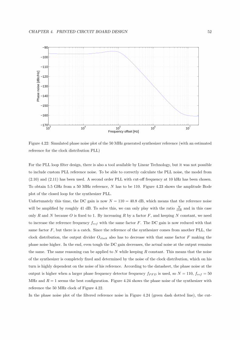
CHAPTER 4. PRINTED CIRCUIT BOARD DESIGN 52
103
104
105
106
107
−170
−160
−150
−140
−130
−120
−110
−100
−90
Frequency offset [Hz]
Pha
se n
oise
[dB
c/H
z]
Figure 4.22: Simulated phase noise plot of the 50 MHz generated synthesizer reference (with an estimated
reference for the clock distribution PLL)
For the PLL loop filter design, there is also a tool available by Linear Technology, but it was not possible
to include custom PLL reference noise. To be able to correctly calculate the PLL noise, the model from
(2.10) and (2.11) has been used. A second order PLL with cut-off frequency at 10 kHz has been chosen.
To obtain 5.5 GHz from a 50 MHz reference, N has to be 110. Figure 4.23 shows the amplitude Bode
plot of the closed loop for the synthesizer PLL.
Unfortunately this time, the DC gain is now N = 110 = 40.8 dB, which means that the reference noise
will be amplified by roughly 41 dB. To solve this, we can only play with the ratio NOR and in this case
only R and N because O is fixed to 1. By increasing R by a factor F , and keeping N constant, we need
to increase the reference frequency fref with the same factor F . The DC gain is now reduced with that
same factor F , but there is a catch. Since the reference of the synthesizer comes from another PLL, the
clock distribution, the output divider Oclock also has to decrease with that same factor F making the
phase noise higher. In the end, even tough the DC gain decreases, the actual noise at the output remains
the same. The same reasoning can be applied to N while keeping R constant. This means that the noise
of the synthesizer is completely fixed and determined by the noise of the clock distribution, which on his
turn is highly dependent on the noise of his reference. According to the datasheet, the phase noise at the
output is higher when a larger phase frequency detector frequency fPFD is used, so N = 110, fref = 50
MHz and R = 1 seems the best configuration. Figure 4.24 shows the phase noise of the synthesizer with
reference the 50 MHz clock of Figure 4.22.
In the phase noise plot of the filtered reference noise in Figure 4.24 (green dash dotted line), the cut-

CHAPTER 4. PRINTED CIRCUIT BOARD DESIGN 53
103
104
105
106
107
−100
−90
−80
−70
−60
−50
−40
−30
−20
−10
0
10
20
30
40
50
f [Hz]
|Clo
sed
loop
| [dB
]
Figure 4.23: Simulated amplitude Bode plot for the synthesizer PLL with N = 110, O = R = 1 and
cut-off frequency 10 kHz
103
104
105
106
107
108
−250
−200
−150
−100
−50
0
Frequency offset [Hz]
Pha
se n
oise
[dB
c/H
z]
TotalVCO filteredReferenceVCO
Figure 4.24: Simulated phase noise plot of the 5.5 GHz LO by the synthesizer (with reference from Figure
4.22)
off frequency of the synthesizer (10 kHz) and the clock distribution (100 kHz) is, as expected, clearly
visible. The phase noise for low offset frequencies is estimated a little below -50 dBc/Hz, which is not
very promising. However, this estimation is pessimistic and by using better reference clocks for the clock

CHAPTER 4. PRINTED CIRCUIT BOARD DESIGN 54
generation PLL this can be much improved. The used reference in these simulations is not the cleanest
clock available. Lowering the cut-off frequency of the clock generation will also improve the integrated
jitter, but will not change the low frequency phase noise (now at -52 dBc/Hz).
4.4.4 I/Q modulator
The LTC5588 requires 2 capacitors to his RF output for output matching (6.8 pF and 0.2 pF). The
differential LO signal is AC coupled and applied to LOP and LOM.
4.4.5 RF amplifier
The GVA-83+ requires external biasing which is applied through a 7.5 Ω resistor. The DC feed needs
a resistance much lower than this 7.5 Ω, and if this is not possible, the then the bias resistor needs to
compensate for this larger DC feed resistance.
It is possible to bypass this amplifier by soldering the two 0 Ω resistors.
4.5 Component placement
This signal generation platform is a mixed-signal board with high speed digital and analog connections.
Digital connections are often very noise and disturb the sensitive analog part of the PCB. To minimize
these disturbances, several countermeasures were taken.
1. The digital components are separated from the analog components. In this design, the digital
components (DAC and clock distribution) are placed on the left side of the board while the analog
component and connectors are on the right side.
2. Where possible, separated power supply distribution can be used to reduce the disturbances intro-
duced by high peak currents in the power supply. The digital power pins of the DAC and the clock
distribution have respectively a separate 1.8 V and 3.3 V distribution.
3. For the same reason as the power supply distribution separation, the digital ground should also be
separated from the analog ground and only be connected to each other on a single point. However
in this design, the DAC needs the digital as well as the analog ground (preferably far away from the
high speed switching digital circuits). In the community, still a large debate is going on concerning
this topic: On a high speed board, large current loops can be formed due to the ground separation
which leads to other problems. So it was decided to keep the digital and analog ground connected.
To ensure good DAC operation, both grounds should be connected near the DAC and as a result
the purpose of separate grounds already loses its use.

CHAPTER 4. PRINTED CIRCUIT BOARD DESIGN 55
As mentioned earlier, layer 2 is fully dedicated to providing a low impedance ground over the complete
board. Layer 5 has a similar purpose on the places where there are layer 4 transmission lines that need
layer 5 as a reference. This is true for the digital LVDS connections from the LPC connector to the DAC.
For all the other components that do not need layer 4 for signal routing, a low impedance power plane is
installed to distribute the power supply to all the pins through a via connection to layer 5. The rest of
layer 5 is filled with ground plane. Setting the gap between de ground plane and the power plane on this
layer to a minimum of 100 µm, gives free decoupling of the power supply and the ground plane.
Figure 4.25 shows a schematic representation of the placement of the most important components together
with the most important connections. At the left, the LPC connector required to connect the FPGA to
the board. This LPC connector carries the 16 bits to the DAC which is situated directly to the right of the
LPC connector. The DAC has to be close to the connector to keep the 16 transmission lines, providing
the 16-bit input data, as short as possible. Almost directly above this DAC is the clock distribution
keeping the clock signal from the distribution to the DAC short. This clock connection has priority to
keep the timing jitter and other effects at a minimum. We choose the pins for the other clock signals
accordingly so they are more or less facing into the desired direction for routing.
The right part of the PCB contains the analog functionality, centered around the I/Q-modulator with the
I and Q channels respectively above and below the component. The RF output goes to the bypassable
RF amplifier to bring the signal, if desired, above 0 dBm. To keep the LO traces short, the synthesizer
is placed between the I-, Q-channel originating from the DAC and going to the I/Q modulator. Figure
B.7 shows a photograph of the top of the soldered PCB.
clock
DAC
synthesizer
I/Q mod.
FM
C c
onn
ecto
r
RF out
Q-filter
I-filter
16 bit LVDS
FPGA clk
Clk outClk in
RF amplifier
Figure 4.25: Visualisation of component placement and most important interconnections

CHAPTER 4. PRINTED CIRCUIT BOARD DESIGN 56
4.6 Off-board connections
Figure 4.26 and Table 4.4 display the desired RF output as well as several test and synchronization
connections provided on the PCB. The test connections are realized by shorting certain connections to
the different connectors by soldering 0 Ω resistors on the anticipated places.
FM
C c
onn
ecto
r
RF out
Clk outClk in
Synthesizer reference
I out
Q out
Figure 4.26: The off-board connections.
4.7 Layout
Appendix B shows the PCB layout of the 6 layers.
4.8 Calculation of NF
To calcaulate the total NF from the analog front-end we need to have all the NFs of the components. The
filter has a worst case NF within the front-end BW) equal to 0.5 dB because it acts as an attenuator, and
the NF of the amplifier is specified in the datasheet as 7.2 dB. The NF of the I/Q modulator is calculated
from the noise floor (-156 dBm/Hz) and conversion gain (-9.1 dB): NF = 174− 156.7 + 9.1 = 26.4 dB.
The total NFtot starting from the filter to the output of the amplifier becomes:
NFtot = 10 log 10
(1.122 +
435.5158
0.8913+
6.2
0.8913 · 0.1230
)= 27.37dB

CHAPTER 4. PRINTED CIRCUIT BOARD DESIGN 57
Name Input/Output Description
RF out Output The RF output of the system.
Clk in Input This is part of the synchronization connections and
provides a way to connect an external clock as ref-
erence for the PLL in the clock distribution. This
Clk in is multiplexed with a reference provided by
the FPGA. The first board in the chain can e.g. get
his reference from the FPGA and provides with Clk
out the other boards with a steady reference.
Clk out Output The second synchronization connection. This output
provides a clock that can be used to feed another
board with this clock as reference.
I out Output A test connection to view the I-channel after filtering.
Q out Output A test connection to view the Q-channel after filter-
ing.
Synthesizer reference Input and Output A test connection to test the Synthesizer reference
provided by the clock distribution or to feed the ref-
erence clock for the PLL of the synthesizer.
Table 4.4: Overview of the provided connections in and out of the board.
This NFtot is mainly determined by the high NF of the I/Q modulator.

Chapter 5
Configuring the Components
Three components (DAC, clock distribution and the synthesizer) require some configuration before they
can execute the desired function. This configuration must be done with Serial Peripheral Interface (SPI),
a 3 wire bus for serial communication. In order to successfully configure the components with the FPGA,
a SPI block with 3 operation modes is designed in digital logic with the help of an Hardware Description
Language (HDL) (Appendix C). This chapter discusses the design of this SPI block and a FSM to control
this SPI block and configure each component one at the time.
5.1 Design of the SPI block
An SPI connection consists of a master and at least one slave. The master always starts the commu-
nication and even provides the common clock signal (Serial Clock (SCLK)) while doing so. If multiple
slaves are present, a slave select (SS or CS) helps the slaves to determine if the data is addressed to
them. Figure 5.1 shows the other necessary connections for SPI where Serial Data Out (SDO) is the
serial data going from the master to the slave and Serial Data In (SDI), the data from slave to master
(the convention in this work is to view everything from the master’s viewpoint).
SPI is technically a 3-wire protocol, however as seen on Figure 5.1, a CS signal for each chip is needed.
This signal is optional if only one slave is present, provided that the slave is always selected. SPI is a de
facto standard so there are a lot of variants, but mostly transmission occurs in frames of 8 bit with at
least 2 frames (one command and one data frame) for each communication cycle. The data is sent MBS
first, unless otherwise mentioned. Other variants exist where e.g. 16 bit commands and data can be sent
or where the option for auto register increment or streaming mode can be turned on.
The master always starts communication by sending the command to the slave. In most cases, the
command only consist of a read or write bit and the register address for the operation. If it is a write, the
master will use the data frame to send the new register content. If the command issues a read operation,
58

CHAPTER 5. CONFIGURING THE COMPONENTS 59
SDO
SDI
SCLK
CS1
CS2
SDI
SDO
SCLK
CS
SDI
SDO
SCLK
CS
Master Slave 1
Slave 2
Figure 5.1: Typical SPI configuration with 2 slaves
the slave sends the register content using the data frame.
The master provides a common clock, SCLK, which is only active when sending or receiving data. When
starting a frame, the master applies the SCLK signal which is an indication for the slave the frame
started. The SCLK signal is low when not sending data, so the first rising edge of SCLK is the start
queue. The data ready to send needs to be applied on the falling edges of SCLK so the receiving end
can sample them at the rising edge. Since SCLK is low when spi is in idle mode, the first bit sent needs
to be set before the SCLK clock starts because SCLK starts with a rising edge. This rising edge already
indicates the first transmitted bit. Figure 5.2 shows an example of a SPI read operation.
SCLK
SDO
SDI
Figure 5.2: A SPI read operation: the master asks the content of register 0x70 (actual command is 0x71,
but the last bit is a read bit) and receives as response 0x2.
Figure 5.3 shows the SPI block pinout while Table 5.1 describes the function of each pin.
Multiple operation modes are supported because there are components on the board that use different
command and frame lengths. Designing an SPI master can easily be done by using an FSM, an input
driver (for sdi) and an output driver (for sdo) (Figure 5.4). The FSM states are the following:

CHAPTER 5. CONFIGURING THE COMPONENTS 60
clk
reset
start
operation_mode
command
address
rnw
data_in
sdi
data_out
data_ready
ack
sclk
sdo
2
16
7
8
8
Figure 5.3: The pinout of the designed SPI-master block
FSM
Input driver Output driver
SCLK driverdata_out
sdi
clk
start
sdo
sclk
com
ma
nd
data
_in
addre
ss
rnw
clk
clk clk
Figure 5.4: Simplified SPI-master block diagram of Figure 5.3
• IDLE : SPI block is waiting for the start signal
• SEND ADDRESS : SPI block is sending the address/command
• SEND DATA : SPI block is sending the data (only used if in write mode)
• RECEIVE DATA : SPI block is receiving data (only used if in read mode)
This FSM controls the flow of one SPI communication cycle (2 frames) (Figure 5.5). When the SPI block is
in IDLE it is ready to receive the start signal. When this happens, the state changes to SEND ADDRESS
which indicates that the master is sending the 8 bit address+rnw or the 16 bit command over the sdo
line. The FSM listens to the sending done signal and changes state to SEND DATA or RECEIVE DATA
depending on the wnr input. After one of these states, the SPI block returns to the IDLE state and
indicates that it is done processing the command.

CHAPTER 5. CONFIGURING THE COMPONENTS 61
Name Input/Output Description
clk Input The clock signal for the module
reset Input Asynchronous reset (active low)
start Input Indicates start of communication
operation mode Input Indicates the operation mode of the SPI block.
(00: normal SPI mode with 7 bit addresses
(LSB=read/write bit), 10: normal SPI mode with 7
bit addresses (MSB=read/write bit) and 8 bit data,
01: 16 bit command and 8 bit data)
command Input 16 bit command (only used when operation mode =
1)
address Input 7 bit register address (only used when opera-
tion mode = 0)
rnw Input 0: write, 1: read
data in Input 8 bit data to be sent over SPI
data out Output 8 bit received data
data ready Output Indicates wheter the SPI block is ready with sending
and or receiving and data out is valid
ack Output Indicates wheter the SPI block has successfully re-
ceived the start command
sclk Output SPI sclk output
sdo Output SPI sdo output
sdi Input SPI sdi input
Table 5.1: SPI block pinout
Both the input and output driver share a common concept, they translate the parallel bits into serial or
the other way around.
There are several ways to accomplish a parallel to serial conversion. One possibility is to use a counter or
FSM and a multiplexer to select the correct bit. This however is not the most optimal implementation.
A far better and more used form in SPI is the use of a shift register for the output driver (Figure 5.6).
At the start of the communication the register is filled and each cycle of the clock, the MSB is shifted
out into the sdo signal. Because there are multiple operation modes with different data widths, the shift
register in Figure 5.6 is 16 bit wide with the 8 most significant bits multiplexed for 8 bit communication.
The design of the input driver is the dual form of the output driver with the sole difference that the bits
received on sdi are shifted into the register (Figure 5.7). After receiving the 8 bits, the data out signal

CHAPTER 5. CONFIGURING THE COMPONENTS 62
IDLE
SEND_ADDRESS
SEND_DATA RECEIVE_DATA
start
done & rnw = 1done & rnw = 0
done
done
Figure 5.5: SPI master FSM
D
enable
clk
QD
enable
clk
QD
enable
clk
QD
enable
clk
Qsdo 0
command[0]
command[7]
command[15]
data/address[7]
command[14]
data/address[6]
Figure 5.6: SPI output driver with shift register (flip-flops are falling edge flip-flops)
contains the received data.
5.2 Configuring the board
For each configurable device on the board (clock distribution, DAC and synthesizer), there are a multiple
of register that need to be set to a specific value. This can be accomplished by configuring each register
of each device in sequence. The easiest way to implement this in digital logic is to design an FSM which
holds track of the device we are programming and a small counter which indicates the register that is
being programmed. The designed FSM has the following states:
• IDLE : Waiting to start the configuration

CHAPTER 5. CONFIGURING THE COMPONENTS 63
enable
clk
DQ
enable
clk
DQ
enable
clk
DQ sdidata_out[7]
data_out[6]
data_out[5]
data_out[0]
Figure 5.7: SPI input driver with shift register (flip-flops are rising edge flip-flops)
• CONFIGURE CLOCK : Configuring the clock distribution chip
• WAIT FOR SPI READY CLOCK : Wait until SPI block set data ready high while programming
one register
• WAIT AFTER CLOCK : Wait 1 clock cycle after having configured the clock distribution chip so
there is time to select the DAC chip
• CONFIGURE DAC : Configuring the DAC
• WAIT FOR SPI READY DAC : Wait until SPI block set data ready high while programming one
register
• WAIT AFTER DAC : Wait 1 clock cycle after having configured the clock distribution so there is
time to select the synthesizer
• CONFIGURE SYNTH : Configuring the synthesizer
• WAIT FOR SPI READY SYNTH : Wait until SPI block set data ready high while programming
one register
• DONE : All registers of all the devices are programmed
The FSM can be divided into 3 parts that behave almost identically because there are 3 devices that
need to be programmed. The FSM for the clock distribution will be explained and the rest speaks for
itself after that. In the CONFIGURE CLOCK state, a new address and its data is applied to the SPI
block and the state changes to WAIT FOR SPI READY CLOCK. WAIT FOR SPI READY CLOCK is
needed to wait until SPI is ready and the register counter is also incremented. These two states go back
and forth until the counter reaches the number of registers that need to be programmed. Then the FSM

CHAPTER 5. CONFIGURING THE COMPONENTS 64
goes to the WAIT AFTER CLOCK state which is needed to enable the chip select for the next device.
The chip always needs to be selected at least one clock cycle before the actual communication starts. This
way, there are no errors that devices hear each others configuration. When the last device (synthesizer)
is configured, the FSM goes into the DONE state, sets the done signal high and stays into this state until
a hard reset is performed. Reconfiguration is only possible after resetting the configure board module.
5.3 FPGA constraints
The constraints used for configuration of the FPGA input and output pins as well as the clocking con-
straints are given in Appendix D.

Chapter 6
Compensation and Pulse Shaping
Filter
In digital communications, the data symbols need to be placed on a transmit pulse (section 2.1.2). In
order to accomplish this, a digital Finite Impulse Response (FIR) filter can be used. Also mentioned
in Chapter 2, a predistortion filter might be needed to compensate for non-ideal amplitude responses
of the system. When both a predistortion and a pulse shaping filter are required, a total filter can be
obtained by convolving the compensation and pulse shaping filter and process the data symbols in one
single combined FIR filter. This chapter explains the design of an FIR filter for the Kintex-7. This FIR
filter is a general FIR filter where the coefficients of the filter taps are configured in lookup tables and if
needed, the filter can be made dynamic reconfigurable. Several topologies are proposed, but only one is
able to pass all the timing constraints for an fDAC = 600 MHz. Before starting the design, it is important
to point out that the symbol rate is 500 Mbaud and the DAC sampling frequency 600 MHz. Section 2.1.2
assumed that Ns is an integer, but in this case, the oversampling is 1.1. There are two possible solutions,
the DAC could be downclocked to 500 MHz to have a Ns = 1 or a resampling filter from 500 MHz to
600 MHz could be used. This chapter discusses the design of a 5 to 6 resampling filter topology. This is
a general topology and it assumes that the FIR filter coefficients are already calculated.
6.1 Normal 500 MHz FIR filter
To begin this chapter, a normal FIR filter is discussed. This is to show the standard FIR filter topology
as the rest of this chapter is based on this. A FIR filter is a digital filter with a finite impulse response
(length Nt, number of taps) and calculating the convolution (6.1) between the input a(k) and the filter
coefficients (or impulse response samples) b(k) is easy to perform in digital logic. This is due to the finite
65

CHAPTER 6. COMPENSATION AND PULSE SHAPING FILTER 66
characteristic of the FIR filter.
y(k) =
Nt−1∑i=0
a(k − i)b(i) (6.1)
In digital logic, this convolution is accomplished by using a shift register for the data a(k− i), where each
register is multiplied with a fixed value b(i). All the outputs from the multipliers are added together. The
addition of the multiplier outputs can be performed by a binary tree adder (Figure 6.1) or a cascaded
adder (Figure 6.2). If timing constraints are not met because the path between the multiplier output and
the filter output is too long, a register can be added between each adder stage. However adding registers
will only work if the addition is fast enough for the clock frequency. Otherwise the clock frequency must
be lowered. The synthesis tool of Xilinx provides a normal FIR filter IP-core which is fast enough for a
500 MHz clock.
a(k-3)
b(3)
a(k-2)
b(2)
a(k-1)
b(1)
a(k)
b(0)
y(k)
Figure 6.1: Normal 4 taps (Ns = 4) FIR filter with binary tree addition
a(k-3)
b(3)
a(k-2)
b(2)
a(k-1)
b(1)
a(k)
b(0)
y(k)
Figure 6.2: Normal 4 taps (Ns = 4) FIR filter with cascaded addition
6.2 Resampling FIR filter
Basic resampling of a digital signal is performed by first upsampling the signal to the lowest common
multiple of both frequencies (in this case 3 GHz) and afterwards decimated to the required frequency.

CHAPTER 6. COMPENSATION AND PULSE SHAPING FILTER 67
For this design, this is done by first introducing 5 zeros between each symbol, filtering the newly created
signal with a low pass filter and afterwards decimate it with a factor 5 to obtain 600 MHz (Figure 6.3).
500 MSPS 3 GSPS 600 MSPS
Figure 6.3: Demonstration of the resampling process (Dotted lines at 600 MSPS are not part of the signal
but only present to show the original signal before downsampling)
Due to the low pass characteristic of the pulse shaping filter, we can use this filter to perform the low pass
filtering of the upsampled signal while simultaneously pulse shaping the symbolstream. The predistortion
filtering can be performed on the 3 GHz signal or the 600 MHz signal as well. If the compensation filter
doesn’t alter the low pass characteristic of the pulse shaping filter, the convolution of the compensation
and the pulse shaping filter can be used for reconstruction of the 3 GHz signal from the 500 MHz signal.
This means that the predistortion filter also has to be a low pass filter with a large enough cut-off
frequency. In this design, this characteristic of the predistortion filter is assumed.
Filtering at 3 GHz with the pulse shaping filter means that Ns needs to be 6 times higher to have the
same performance as the normal 500 MHz FIR filter. This is also true for the predistortion filter. Another
problem is that a 3 GHz clock is needed to filter the internal 3 GHz sample signal. This is obviously
not possible on an FPGA. A solution that most of the time works to lower the clock speed is to use
several parallel datastreams that when combined together form the data at the faster clock rate. When
performing upconversion, splitting in different datastreams is particular straight forward when you take
the effect of introducing zeros in between the samples into account [19]. So when we go from 500 MHz to
3 GHz, we have 5 zeros between the symbols and that means that for each 6 multipliers, 5 multipliers are
actually doing nothing. If we keep track of the multipliers that are active, we see that they are 6 samples
apart and shift each clock frequency one place. Using this knowledge, 6 new filters can be obtained from
the original FIR filter. Each new filter is a decimated version with decimation factor 6 of the original
filter, but each one starts the decimation one sample later than the filter before him. To conveniently
address the filters, we number them filter 1 to 6 with filter one starting his decimation at b(0) and filter 6
at b(5). By applying the original datastream (without adding the 5 zeros) to each filter, filter 1 will give
y(0), filter 2 y(1), . . . , filter 6 y(5), filter 1 again y(6), and so on. We actually have created 6 parallel
filters that act on the same inputstream and when performing parallel to serial conversion, we have the
wanted 3 GHz signal (Figure 6.4). Due to the 6 parallel filters, the clock rate for each filter only has to
be 500 MHz, the original data rate.
For a resample filter, actually, the 3 GHz signal is only an intermediate side product that is only internally

CHAPTER 6. COMPENSATION AND PULSE SHAPING FILTER 68
needed. The output signal is a by 5 decimated version of the 3 GHz sampled intermediate signal. It
is actually not necessary to fully reconstruct the 3 GHz sampled signal from the 6 stream to decimate
it. Decimation can be performed directly on the 6 streams. Table 6.1 shows the order of taking the the
outputs.
filter 1
filter 2
filter 3
filter 4
filter 5
filter 6
a(k) P/S y(k)
500 MHz 3 GHz
Figure 6.4: Parallel stream upsampling filter for conversion from 500 MHz to 3 GHz
Sample number Take sample from
1 filter 1
2 filter 6
3 filter 5
4 filter 4
5 filter 3
6 filter 2
7 filter 1...
Table 6.1: Order of taking the samples from each filter for directly decimation of the parallel streams to
600 MHz
As a result, each filter has to run at 600 MHz, and a global FSM takes each clock cycle a sample from
one filter in the specified order in Table 6.1. However, there is a catch. Due to the 6 parallel streams
and only decimation by 5, the samples taken from filter 1 and filter 6 afterwards, need act on the same
input. This means that the data may not shift between filter 1 and filter 6. Symbolically this becomes,
with yi(k) the kth output sample from filter i: y1(0), y6(0), y5(1), y4(2), . . . , y2(4), y1(5), . . .

CHAPTER 6. COMPENSATION AND PULSE SHAPING FILTER 69
This is also intuitively explainable. The data is applied at 500 MHz, but the filter takes it at 600 MHz,
so for each 5 samples the filter takes, it needs to wait one clock to resynchronize with the input data rate
at 500 MHz. One other problem is that there is a need for Clock Domain Crossing (CDC) circuitry to
pass the input data at 500 MHz to the 600 MHz clocked filters. Before continuing about the optimization
of the resample filter, CDC is first investigated.
6.3 Clock Domain Crossing
Clock Domain Crossing (CDC) is passing data between two digital systems with a different clock frequency
or the same frequency but a different phase. It is clear that a simple synchronizing flip-flop at the receiver
side (Figure 6.5) does not suffice since the receiving clock region can clock the data received at any time
even when it is not yet stable. The setup and hold times of the flip-flop will most likely be violated which
causes metastability and invalid data that travels across the design.
When a flip-flop enters the metastable or quasi-stable state, its output oscillates between 0 and 1 and
finally settles. The outcome is unpredictable and hence metastability must always be avoided. Depending
on the application there are several synchronization solutions.
clk A clk B
data
A B
Figure 6.5: Single flip-flop synchronizer
6.3.1 Two flip-flop synchronizer
If the signal that needs to cross a clock domain region is relatively slow in comparison to the clock
frequency of the receiving end, two synchronizing flip-flops instead of one can be used (Figure 6.6).
While the first flip-flop is in a metastable state, the second holds his previous value. The next clock cycle
(assuming that the data didn’t change), the first synchronizing flip-flop will now read the stable input
signal and the signal is synchronized. This type of synchronization is particularly not a safe solution as
data can be lost during the transaction but it is by far the fastest method.

CHAPTER 6. COMPENSATION AND PULSE SHAPING FILTER 70
clk A clk B clk B
data
A B
Figure 6.6: Two flip-flop synchronizer
6.3.2 Closed loop handshake synchronizers
A method for reliable transfer of data between two asynchronous systems is by means of a handshake.
This method is particularly useful in lower speed links where reliable data transfer is of the issue. The
transmitting side signals the receiver that the data is stable and when the receiver acknowledges the
transmitting side that he has successfully received the data. If the transmitter sees the acknowledge,
he acknowledges the receiver for his acknowledge signal and the transaction is finished. There are other
variants which use more acknowledge signals, but the previous mentioned data stable, ack and ack t are
always necessary. It usually takes a lot more clock cycles than the simple two flip-flop synchronization to
successfully finish a data transaction. Due to the two-way handshake, this is often called a closed loop
data transfer.
6.3.3 First In First Out buffers
When in need of a constant (high speed) reliable data throughput (e.g. for a FIR filter), both above men-
tioned synchronizers are not the most optimal solutions: the two flip-flop synchronizer is fast, but there
is a possibility of data loss and the handshake synchronizer takes too much clock cycles to complete. The
solution to this problem is the use of an asynchronous First In First Out (FIFO) buffer. An asynchronous
FIFO is a FIFO where the input clock is different from the output clock. This makes the design of the
FIFO more challenging. This section briefly handles the design of a high speed asynchronous FIFO for
the Kintex-7.
The first choice for a FIFO is which type of memory to use. For an asynchronous FIFO it is mandatory
to be able to randomly access the data in the memory and hence for a small FIFO this could be a regis-
terbank and for a large FIFO, a Random-Access Memory (RAM) block.
This memory will then be used as a circular memory by the input and output ports. The input and
the output remember the current memory location they respectively have to read from and write to.
Each clock cycle, this address (input address with input clock and output address with output clock) is

CHAPTER 6. COMPENSATION AND PULSE SHAPING FILTER 71
incremented by 1 and when it reaches the maximal memory address, it wraps back to 0. There also needs
to be a safety check that the output address may never pass the input address (this would mean that the
buffer is full and is going to overflow). This FIFO so far is still not safe when input and output address
are the same. This happens when the FIFO is nearly empty. Other problems with asynchronous FIFO is
the generation of the full and empty signals. For the generation of the empty and full signals, the input
and output addresses both at a different clock frequency need to be compared.
Gray counter and read/write offset
One step into the direction of making the asynchronous FIFO safer is to introduce gray counters for the
input and output addresses instead of a normal binary counter. In a gray counter, only one bit changes
when incrementing. So when the address needs to be transferred from one clock region to the other, only
one bit can be received wrong and cause instability. This is much safer than the binary counter where
multiple bits can change when incrementing. One other advantage for using a gray counter over a binary
counter is that a gray counter is much faster because every bit after incrementing can be calculated with
a single Lookup Table (LUT) table, while a binary counter is mostly implemented as a ripple adder which
requires multiple cascaded LUTs. The gray addresses can directly be fed to the memory block because it
does not matter if we fill the memory linearly or in a seemingly random order. The only requirement is
that both input and output use the same type of datarepresentation of the address, a gray representation
in this case.
To solve the problem where read and write pointers of the memory module are very close to each other,
the output address can start at an offset from the input address so he always lacks behind the input even
when the FIFO is empty. The minimal offset needed depends on the difference in the input and output
clock and is hence very specific for each application.
Generation of the empty and full signals
The generation of the empty and the full signals requires crossing the clock domain for both the input and
output addresses. This needs to be fast so e.g. a two flip-flop synchronizer can be used together with a
pessimistic calculation of the empty and full signals. This means that the empty and full signal are longer
high or low than necessary in order to make sure that both input and output clock are able to react on
them. The empty signal is read at the output clock rate, but the calculation uses the two times delayed
version of the input address. For the full signal the opposite is true. Due to the synchronization process,
the emtpy and full signals can only be an estimation of the actual empty and full status, so a pessimistic
calculation is absolutely necessary. Figure 6.7 shows the full block diagram of the asynchronous FIFO
[5].
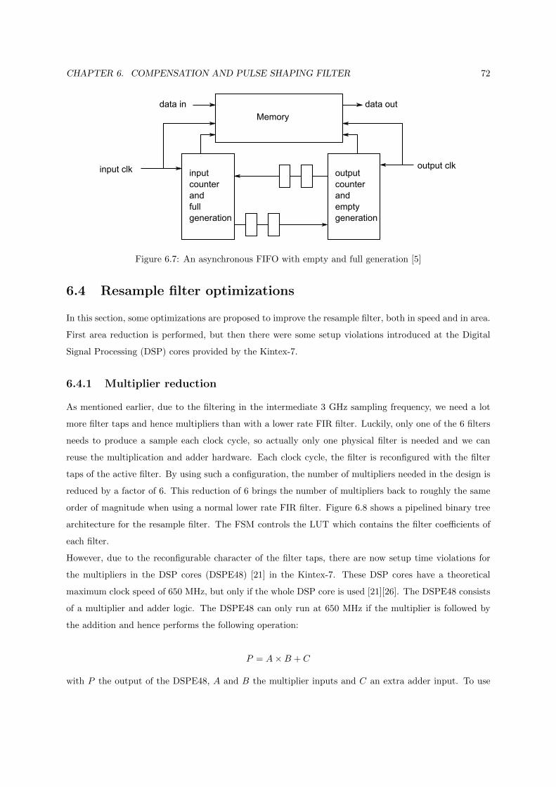
CHAPTER 6. COMPENSATION AND PULSE SHAPING FILTER 72
input
counter
and
full
generation
Memory
output
counter
and
empty
generation
input clk output clk
data in data out
Figure 6.7: An asynchronous FIFO with empty and full generation [5]
6.4 Resample filter optimizations
In this section, some optimizations are proposed to improve the resample filter, both in speed and in area.
First area reduction is performed, but then there were some setup violations introduced at the Digital
Signal Processing (DSP) cores provided by the Kintex-7.
6.4.1 Multiplier reduction
As mentioned earlier, due to the filtering in the intermediate 3 GHz sampling frequency, we need a lot
more filter taps and hence multipliers than with a lower rate FIR filter. Luckily, only one of the 6 filters
needs to produce a sample each clock cycle, so actually only one physical filter is needed and we can
reuse the multiplication and adder hardware. Each clock cycle, the filter is reconfigured with the filter
taps of the active filter. By using such a configuration, the number of multipliers needed in the design is
reduced by a factor of 6. This reduction of 6 brings the number of multipliers back to roughly the same
order of magnitude when using a normal lower rate FIR filter. Figure 6.8 shows a pipelined binary tree
architecture for the resample filter. The FSM controls the LUT which contains the filter coefficients of
each filter.
However, due to the reconfigurable character of the filter taps, there are now setup time violations for
the multipliers in the DSP cores (DSPE48) [21] in the Kintex-7. These DSP cores have a theoretical
maximum clock speed of 650 MHz, but only if the whole DSP core is used [21][26]. The DSPE48 consists
of a multiplier and adder logic. The DSPE48 can only run at 650 MHz if the multiplier is followed by
the addition and hence performs the following operation:
P = A×B + C
with P the output of the DSPE48, A and B the multiplier inputs and C an extra adder input. To use

CHAPTER 6. COMPENSATION AND PULSE SHAPING FILTER 73
a(k-3)
a(k-2)
a(k-1)
a(k)
y(k-4)
LUT
LUT
LUT
LUT
FSM
Figure 6.8: A binary tree addition resample FIR filter (pipelined)
this DSPE48 at its full potential, the outputs of the multiplier need to be added in cascade instead of
the binary tree addition.
6.4.2 Fully pipelined cascaded 500 MHz to 600 MHz resample FIR filter
The internal structure of the DSPE48 asks for cascaded addition as in Figure 6.2. For a binary tree
addition like in Figure 6.1 it is straight forward to make a pipelined version. For a cascaded addition,
it is a bit more complicated since dummy flip-flops are needed to delay the paths that only contribute
at the very end of the addition chain (Figure 6.9). Some of these flip-flops can be moved before the
multiplication and after rearranging Figure 6.10 is obtained. This means that we can divide the cascaded
filter into standard cells which is exactly the functionality of the DSPE48 core. So by using this topology
it is possible to run the filter at 600 MHz.
b(3)
b(2)
b(1)
a(k)
b(0)y(k-5)
Figure 6.9: A pipelined cascaded addition FIR filter
This pipelined cascaded FIR filter is however not suited for dynamic reconfiguration unless reconfiguration

CHAPTER 6. COMPENSATION AND PULSE SHAPING FILTER 74
b(3)
b(2)
b(1)
a(k)
b(0)
y(k-6)
0
Standard cell
Figure 6.10: A pipelined cascaded addition FIR filter with standard cells
information is also passed down the pipeline so that each cell can generate its own coefficient based on
this information. Each cell receives the filter number or state from which it has to take the coefficient
and generates based on that state the state for the next cell in line (Figure 6.11). The first cell receives
its state from the global FSM. With this topology, it is impossible to hold the data for one clock cycle
for filter 6, because of the pipelining. Therefore, a separate pipelined normal FIR filter solely for filter
6 is used. This means that to solve the setup time violations of the DSPE48, we can only reduce the
number of filter taps by a factor of 3.
LUTNext
state
state in
state out
A B
A'
B'
Figure 6.11: The complete standard cell with coefficient generation for the pipelined cascade adder FIR
filter
When implementing this design for the Kintex-7, after optimizing for the timing, still 10 hold time issues
remained. These can be solved by introducing data buffers to delay the data, but this would probable
lead to other timing issues as well so in this design we have chosen to first try another approach for the
filter instead of introducing these buffers.

CHAPTER 6. COMPENSATION AND PULSE SHAPING FILTER 75
6.4.3 Split binary tree adder 500 MHz to 600 MHz resample FIR filter
It is clear that a 600 MHz FIR filter for the FPGA used in this design is sometimes a bit too fast to meet
all the timing constraints. With this in mind, a resample topology, still based on the 6 parallel filter, but
now instead of combining them into 1 physical filter where we constantly change the filter coefficients, we
combine them into 2 lower frequency filters running each at 300 MHz (Figure 6.12) and provide switching
circuits for the splitting and recombination of both filter outputs. To avoid name confusion, these 2
physical Filter are called with the capital letter F to distinguish them from the filter 1 to 6: Filter 1
and Filter 2. Filter 2 runs ahead of Filter 1 and hence its shift register is a by one shifter version of the
shift register of Filter 1 (except when in state filter 6 ). Now that each filter only runs at 300 MHz, the
topology of Figure 6.8 meets all the constraints.
The switching circuit before Filter 1 and 2 acts as the 600 to 300 MHz conversion system that switches
each clock cycle the data to either the first or the second filter. Each individual internal Filter still needs
to filter all the data, so an extra port (previous data in) and small changes to the normal filter in Figure
6.8 need to be made.
filter 1, filter 5, filter 3
filter 6, filter 4, filter 2
switching
block
Filter 1
Filter 2
500 MHz 600 MHz 300 MHz 600 MHz
P/S
Figure 6.12: Resample FIR filter topology with two parallel lower rate filter streams
Internal FIR Filter
Since each of the two internal FIR Filters only runs at 300 MHz, but accepts data that is clocked at 600
MHz, they need to shift their shift register not one, but two places each clock cycle of their 300 MHz
clock. Therefore they need two input ports which are named data in and data in previous. For Filter 2,
data in previous holds the same data as Filter 1’s data in port and the data in previous of Filter 1 holds
the previous data in of Filter 2. These two input ports supply the data that is clocked respectively in
the first and second register of the shift register. Each Filter has its own FSM to decide which of the
three filter coefficients to use. This FSM is also used to know when the input data needs to be stalled
(for filter 6). Actually due to the lower clock speed in Filter 1 and 2, the word stalled is now misplaced.
Each Filter always shifts its shift register by two, but when Filter 2 is in the state filter 6, it needs the
same data as Filter 1. In this case, Filter 2 only needs to shift its shift register by one and instead of
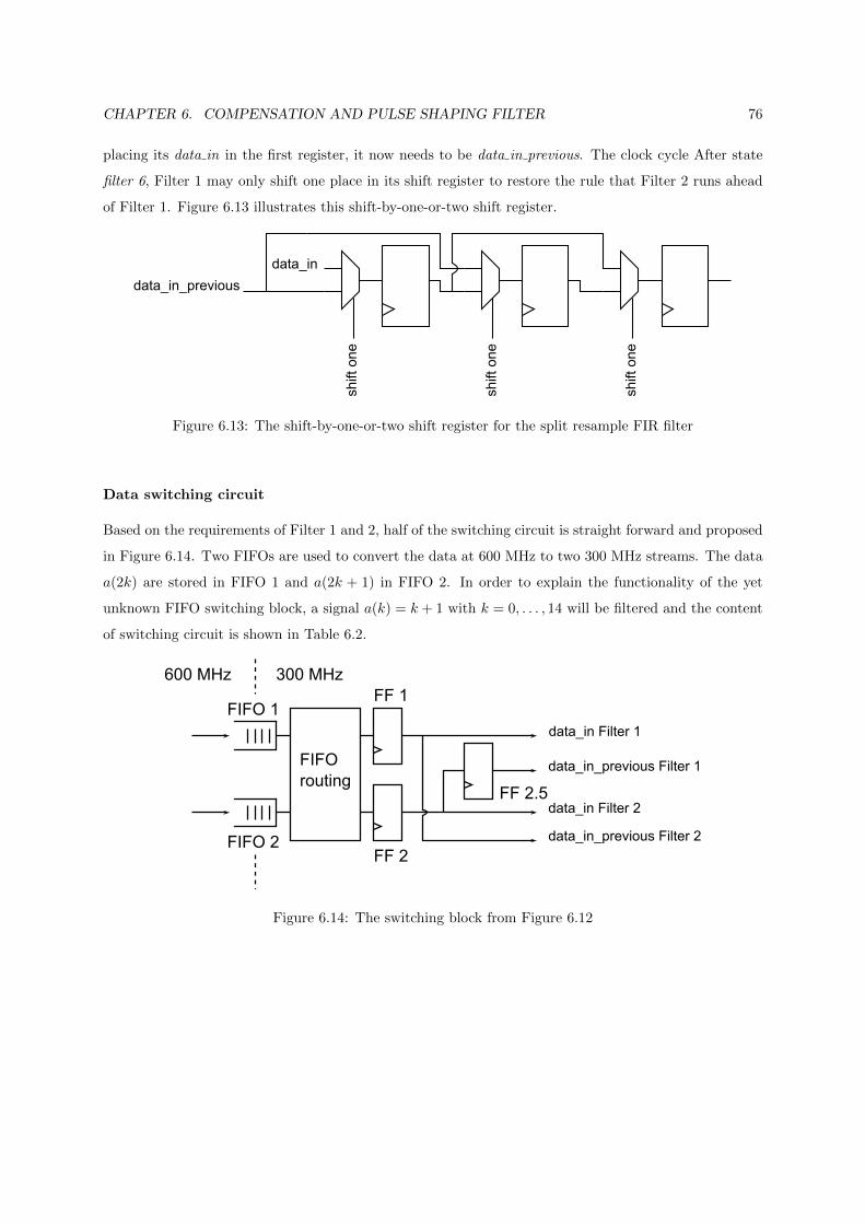
CHAPTER 6. COMPENSATION AND PULSE SHAPING FILTER 76
placing its data in in the first register, it now needs to be data in previous. The clock cycle After state
filter 6, Filter 1 may only shift one place in its shift register to restore the rule that Filter 2 runs ahead
of Filter 1. Figure 6.13 illustrates this shift-by-one-or-two shift register.
data_in
data_in_previous
shift one
shift one
shift one
Figure 6.13: The shift-by-one-or-two shift register for the split resample FIR filter
Data switching circuit
Based on the requirements of Filter 1 and 2, half of the switching circuit is straight forward and proposed
in Figure 6.14. Two FIFOs are used to convert the data at 600 MHz to two 300 MHz streams. The data
a(2k) are stored in FIFO 1 and a(2k + 1) in FIFO 2. In order to explain the functionality of the yet
unknown FIFO switching block, a signal a(k) = k + 1 with k = 0, . . . , 14 will be filtered and the content
of switching circuit is shown in Table 6.2.
FIFO
routing
data_in Filter 1
data_in Filter 2
data_in_previous Filter 1
data_in_previous Filter 2
FIFO 1
FIFO 2
FF 1
FF 2
FF 2.5
600 MHz 300 MHz
Figure 6.14: The switching block from Figure 6.12

CHAPTER 6. COMPENSATION AND PULSE SHAPING FILTER 77
FIF
O1
FIF
O2
FF
1F
F2
FF
2.5
shif
t1.1
shif
t1.2
shif
t1.3
shif
t2.1
shif
t2.2
shif
t2.3
Fil
ter
1/F
ilte
r2
state
12
00
00
00
00
0-
34
12
00
00
00
0-
56
43
21
00
10
01/6
76
45
32
10
32
15/4
98
67
54
32
54
33/2
1110
98
76
54
65
41/6
1112
910
87
65
87
65/4
1314
1112
109
87
10
98
3/2
. . .. . .
. . .. . .
. . .. . .
. . .. . .
. . .. . .
. . .. . .
Tab
le6.
2:F
un
ctio
nal
ity
ofth
esw
itch
ing
circ
uit
wh
enfi
lter
inga(k
)=k
+1
wit
hk
start
ing
from
0

CHAPTER 6. COMPENSATION AND PULSE SHAPING FILTER 78
Based on Table 6.2, it seems that each time Filter 1 and Filter 2 are in state 1/6, the routing of data from
the FIFOs needs to be switched from FF 1 to FF 2 or the other way around. The reason for this is that
when in state 1/6, Filter 2 only shifts one and it ignores its current data in. However this data sample
may not get lost and hence a stall on FIFO 2 is necessary. After state 1/6, FF 2.5 is temporarily routed
to data in previous to recover from the possible data loss by ignoring data in. Due to this stall, FIFO 2
now runs behind FIFO 1 and rerouting the outputs of the FIFOs to FF 1 and FF 2 is needed. The next
time in state 1/6, FIFO 1 needs to be stalled (as he now connects to FF 2) and the circle is complete.
Figure 6.15 demonstrates the full switching circuit. For simplicity and readability of the schematic, not
all the control signals are shown.
data_in Filter 1
data_in Filter 2
data_in_previous Filter 1
data_in_previous Filter 2
FIFO 1
FIFO 2
FF 1
FF 2
FF 2.5
600 MHz 300 MHz
Figure 6.15: The full switching block from Figure 6.12 with FIFO routing

Chapter 7
Measurements
This chapter summarizes and discusses the most important measurements performed in order to test and
debug the system. The board has been soldered and tested in small steps so every part could be tested
before moving on to the next part. In the end everything is connected and the performance of the full
system is evaluated.
7.1 Testing the clock distribution
Figure 7.1 and Figure 7.2 show respectively the spectrum and time domain signal of the measured 50
MHz clock distributed by the clock distribution. The time domain signal should switch from 0 V to 3.3
V, but this is a measurement into a 50 Ω load. When providing a high impedant load, this will lead to
3.3 V amplitude.
The phase noise performance of this 50 Ω clock has also been tested for two PLL reference inputs: A
50 MHz reference provided by the FPGA and a 50 MHz reference provided by a clean signal generator.
Figures 7.3 and 7.4 are the phase noise plots for respectively the FPGA and the signal generator reference.
The performance of the clock generator highly depends on the reference, which is clearly visible on these
figures. The reference provided by the FPGA goes through the complete clock routing of the FPGA
before leaving it. This leaves a rather noisy reference for the clock generator, especially for lower offset
frequencies. Table 7.1 displays the total measured phase noise. The phase noise plots are more or less
consistent with the simulated characteristic, but due to the different references used, the jitter can be
better or worse than the simulation depending on the reference used.
79

CHAPTER 7. MEASUREMENTS 80
0 1 2 3 4 5 6 7 8 9 10
x 108
−40
−30
−20
−10
0
10
20
f [Hz]
Pow
er [d
Bm
]
Figure 7.1: Measured (frequency domain) 50 MHz clock generated by the clock generator
−1 −0.8 −0.6 −0.4 −0.2 0 0.2 0.4 0.6 0.8 1
x 10−7
−0.2
0
0.2
0.4
0.6
0.8
1
1.2
1.4
1.6
1.8
Time [s]
Vol
tage
[V]
Figure 7.2: Measured (time domain) 50 MHz clock generated by the clock generator
7.2 Testing the DAC and anti-imaging filter
7.2.1 FPGA-DAC interface
The most critical part of working with a DAC is that the digital interface of the DAC sees the correct
bits. The reason for errors in the digital interface is timing differences and delays between data and DCI

CHAPTER 7. MEASUREMENTS 81
102
103
104
105
106
−140
−130
−120
−110
−100
−90
−80
−70
−60
−50
−40
Frequency offset [Hz]
Pha
se n
oise
[dB
c/H
z]
Figure 7.3: Measured phase noise of the 50 MHz generated clock with the reference from the FPGA
102
103
104
105
106
−140
−130
−120
−110
−100
−90
−80
Frequency offset [Hz]
Pha
se n
oise
[dB
c/H
z]
Figure 7.4: Measured phase noise of the 50 MHz generated clock with the reference from the signal
generator
signal. In order to test this interface, a 50 MHz square wave I and a constant Q is generated. The reason
for this signal is that due to the DDR digital interface, a constant Q and non constant I means that every
rising and falling edge of the DCI, the amplitude would switch from a 1 to a 0 or the other way around.
The same could also be achieved by setting Q to 0 and I to another constant, but then crosstalk between

CHAPTER 7. MEASUREMENTS 82
FPGA reference Signal generator reference
θjitter,rms 2 0.0920
tjitter,rms 117 ps 5.11 ps
Table 7.1: Phase noise summary of the 50 MHz generated clock (integrated from 100 Hz to 1 MHz)
I and Q due to timing errors cannot be properly viewed. After generating this signal, there are two places
where you can check for errors: At the digital interface itself to check if the bits are sent correctly over
the critical LVDS transmission lines and the analog output, to see if there is any crosstalk (due to timing
errors) between the I and Q channel. Figure 7.5 shows the signal received from one bit at the end of the
LVDS transmission line. This signal looks what we expect and this concludes that the LVDS lines are
correct, they do not distort the signal too much. The output of the analog I and Q channel are also as
expected (50 MHz square at I and 0 at Q) and this concludes that the LVDS lines do not introduce any
timing errors.
−5 −4 −3 −2 −1 0 1 2 3 4 5
x 10−8
−0.3
−0.2
−0.1
0
0.1
0.2
0.3
0.4
0.5
0.6
Time [s]
Vol
tage
[V]
Figure 7.5: Measured waveform of one bit of the FPGA-DAC interface when transmitting 50 MHz square
wave on I and 0 on Q
7.2.2 Signal distortion
The performance of the analog DAC outputs can be investigated by measuring the harmonics when
transmitting a single frequency and intermodulation between multiple frequencies. For the measurement
of the harmonics, a distinction can be made between a frequency that is an integer division of the sample

CHAPTER 7. MEASUREMENTS 83
frequency (600 MHz) e.g. 200 MHz and other frequencies, e.g. 17 MHz. The reason for this distinction
is that a harmonic of e.g. 200 MHz will evidently fall on 600 MHz and its harmonics, which can increase
the power of the harmonics. Figures 7.6 and 7.7 show respectively the output spectrum of a 200 MHz
generated sine and a 17 MHz generated sine wave. Both spectra show harmonic distortion (power at
fundamental frequency - power at highest distortion frequency) below -30 dB which is a requirement of
most communication systems.
0 1 2 3 4 5 6 7 8 9 10
x 108
−140
−120
−100
−80
−60
−40
−20
0
f [Hz]
Pow
er [d
Bm
]
Figure 7.6: Measured spectrum of a generated 200 MHz sine wave (Power at 200 MHz is -6 dBm)
The intermodulation distortion is measured by inserting three tones with the same power: one at 50
MHz, 100 and 200 MHz. The total signal is normalized so the maximum peak is equal to the largest
DAC value (Figure 7.8). Since these three frequencies are a multiple of each other, the intermodulation
frequencies also fall on harmonic frequencies of the single tones. Hence, this measurement is a worst case
scenario, but the worst intermodulation distortion at 400 MHz (-48 dBm) is still 34 dB lower than the
power of each fundamental frequency (-14 dBm).
7.2.3 DAC jitter
To test the influence of the clock on the DAC, the phase noise of a single tone can be measured. Figure
7.9 shows the phase noise plot of a 17 MHz generated sine wave. This measurement has been made with
the reference from the FPGA, which is clearly visible, but apart from that, the signal shows good phase
noise performance. We were unable to test the phase noise of the DAC with the cleaner signal generator
because the other connections were already soldered after applying and testing the cleaner reference.

CHAPTER 7. MEASUREMENTS 84
0 1 2 3 4 5 6 7 8 9 10
x 108
−140
−120
−100
−80
−60
−40
−20
0
f [Hz]
Pow
er [d
Bm
]
Figure 7.7: Measured spectrum of a generated 17 MHz sine wave (Power at 17 MHz is -6 dBm)
0 1 2 3 4 5 6 7 8 9 10
x 108
−140
−120
−100
−80
−60
−40
−20
0
f [Hz]
Pow
er [d
Bm
]
Figure 7.8: Measured spectrum of a three equal power tones at 50, 100 and 200 MHz (Power of funda-
mental tones -14 dBm)
7.2.4 Filter bandwidth
To test the performance of the anti-imaging filter, a chirping cosine up until 300 MHz is generated in the
FPGA. Figure 7.10 shows the measured spectrum of this chirp signal and shows that the cut-off frequency

CHAPTER 7. MEASUREMENTS 85
102
103
104
105
106
−140
−130
−120
−110
−100
−90
−80
−70
−60
−50
Frequency offset [Hz]
Pha
se n
oise
[dB
c/H
z]
Figure 7.9: Measured phase noise of a generated 17 MHz sine (with FPGA clock as reference for clock
generation)
lies around 250 MHz. This is a little less than expected, but can be compensated.
0 1 2 3 4 5 6 7
x 108
−60
−50
−40
−30
−20
−10
0
f [Hz]
S(f
)/S
(0)
[dB
]
Figure 7.10: Measured anti-imaging filter by sending a chirping cosine with frequency up until 300 MHz

CHAPTER 7. MEASUREMENTS 86
7.3 Testing the synthesizer
The performance of the synthesizer depends on the performance of the clock generator and hence the
performance of the reference provided to the clock generator. Testing the synthesizer is as straight
forward as measuring the output spectrum and phase noise. Figure 7.11 shows the output spectrum
(with the clock reference generated by the clean signal generator) while Figure 7.12 shows the phase
noise performance of the synthesizer for a 10 kHz PLL loop BW. A single ended LO power of -7 dBm is
obtained, which will lead to a -4 dBm differential LO power. We expect to see on Figure 7.12 a cut-off
at 10 kHz. Starting from 100 kHz offset, the phase noise in Figure 7.12 starts to decay faster due to
the 100 kHz cut-off in the clock generator. For the measurement in Figure 7.12, the total phase noise is:
θjitter,rms = 4.02 or equivalently tjitter,rms = 2.03 ps (integrated from 100 Hz to 1 MHz).
5.494 5.496 5.498 5.5 5.502 5.504 5.506
x 109
120
100
80
60
40
20
0
f [Hz]
Pow
er
[dB
m]
-7.6 dBm
Figure 7.11: Measured spectrum of the LO generated by the synthesizer at 5.5 GHz
7.4 Testing the I/Q modulator
Testing the I/Q modulator alone is not possible since the DAC and the synthesizer are always connected
to the I/Q modulator. In this section the full system without the RF amplifier is tested. Figure 7.13
shows the output of the I/Q modulator when generating a 17 MHz sine in the DAC and an LO at 5.5
GHz. The LO is more than 30 dB suppressed with respect to the output power of the wanted signals
at 5.483 and 5.517 GHz (-14 dBm). The I/Q modulator has a conversion gain of -9 dB at 6 GHz, so
if we look at Figure 7.7 and take into account that this was measured single ended we roughly have -3
dBm at the input of the I/Q modulator. This means that we expect around -15 dBm as output (-9 dB

CHAPTER 7. MEASUREMENTS 87
102
103
104
105
106
−130
−120
−110
−100
−90
−80
−70
−60
−50
Frequency offset [Hz]
Pha
se n
oise
[dB
c/H
z]
Figure 7.12: Measured phase noise of the 5.5 GHz LO generated by the synthesizer with a PLL loop BW
of 10 kHz (with the reference from signal generator for clock generation)
conversion gain and -3 dB because of the two peaks). We have -14.87 dBm, but this measurement is for
both I and Q combined, sot we only have -18 dBm for the I and the Q channel separately. We have lost 3
dB somewhere in between, but this can be due to unavoidable parasitics and poorly matched interfaces.
7.5 Full system with RF amplifier
Figures 7.14 to 7.16 show the measurement results of the full system with RF amplifier. As can be seen
on the figures, the gain is not flat over the complete 500 MHz RF BW. This is not a problem that lies
with the I/Q modulator BW because even when transmitting a 17 MHz signal (Figure 7.14), both the
upper and lower RF frequency signals are different in power while Figure 7.13 shows that they are the
same after the I/Q modulator. Tests also show that the I/Q modulator has a large enough BW. The
problem that causes this is the use of a discrete component bias tee. The DC feed inductor has only a
SRF of 5800 MHz which is very close to the maximum frequency in the system. Also due to the fact
that it is hard to fabricate large inductor values with a large enough SRF (5900 GHz, still very low given
the application), we could only use a 4.3 nH inductor which is only 150 Ω at 5.5 GHz. A change in
the frequency changes the impedance of the inductor, but due to this rather low inductance value, this
change is rather high compared with the impedance change when using a high inductance value. Also
due to the discrete component bias tee, the matching to 50 Ω is not what it needs to be, so there are
also extra losses due to matching. To see what happens at other frequencies, the LO frequency has been
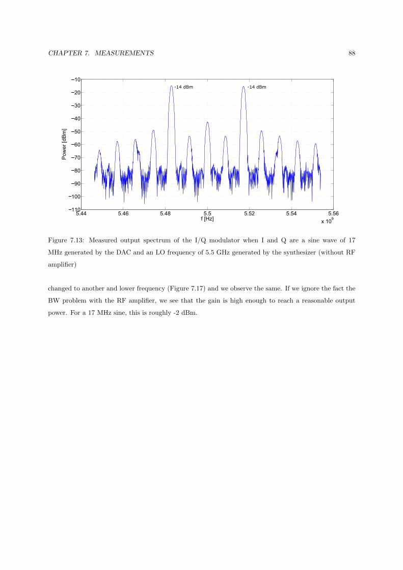
CHAPTER 7. MEASUREMENTS 88
5.44 5.46 5.48 5.5 5.52 5.54 5.56
x 109
110
100
90
80
70
60
50
40
30
20
10
f [Hz]
Pow
er
[dB
m]
-14 dBm-14 dBm
Figure 7.13: Measured output spectrum of the I/Q modulator when I and Q are a sine wave of 17
MHz generated by the DAC and an LO frequency of 5.5 GHz generated by the synthesizer (without RF
amplifier)
changed to another and lower frequency (Figure 7.17) and we observe the same. If we ignore the fact the
BW problem with the RF amplifier, we see that the gain is high enough to reach a reasonable output
power. For a 17 MHz sine, this is roughly -2 dBm.

CHAPTER 7. MEASUREMENTS 89
5.45 5.46 5.47 5.48 5.49 5.5 5.51 5.52 5.53 5.54 5.55
x 109
100
90
80
70
60
50
40
30
20
10
0
f [Hz]
Pow
er
[dB
m]
-2.16 dBm -3.14 dBm
Figure 7.14: Measured output spectrum of the I/Q modulator when I and Q are a sine wave of 17 MHz
generated by the DAC and an LO frequency of 5.5 GHz generated by the synthesizer (with RF amplifier)
5.2 5.3 5.4 5.5 5.6 5.7 5.8
x 109
90
80
70
60
50
40
30
20
10
0
10
f [Hz]
Pow
er
[dB
m]
1.77 dBm
-7.12 dBm
Figure 7.15: Measured output spectrum of the I/Q modulator when I and Q are a sine wave of 250 MHz
generated by the DAC and an LO frequency of 5.5 GHz generated by the synthesizer (with RF amplifier)

CHAPTER 7. MEASUREMENTS 90
5.2 5.3 5.4 5.5 5.6 5.7 5.8
x 109
90
80
70
60
50
40
30
20
10
0
10
f [Hz]
Pow
er
[dB
m]
3.26 dBm
-6.38 dBm
Figure 7.16: Measured output spectrum of the I/Q modulator when I and Q are a sine wave of 200 MHz
generated by the DAC and an LO frequency of 5.5 GHz generated by the synthesizer (with RF amplifier)
5.27 5.28 5.29 5.3 5.31 5.32 5.33 5.34 5.35 5.36
x 109
90
80
70
60
50
40
30
20
10
0
10
f [Hz]
Pow
er
[dB
m]
4.07 dBm 2.17 dBm
Figure 7.17: Measured output spectrum of the I/Q modulator when I and Q are a sine wave of 17 MHz
generated by the DAC and LO frequency 5.315 GHz generated by the synthesizer (with RF amplifier)

Chapter 8
Conclusions
In this Master Thesis, a broadband signal generation platform for 5G and attocell applications has been
designed. This platform is able to generate a 500 MHz BW RF signal on a 5.5 GHz carrier. In the
previous chapters, the design and testing of this platform has been discussed. This chapter summarizes
these results and the remaining problems with their possible solutions. We end this chapter with a small
future work.
8.1 Results
The signal generation platform consists of a digital and an analog part. The analog front-end converts
the digital signal generated by the digital part in the FPGA in de DAC and upconverts it to 5.5 GHz.
Both the clock for the DAC and FPGA and the LO are generated on the board. Every part of the PCB
has been tested separately before connecting and testing the whole system.
The most critical part of the DAC was the design of the 16 impedance matched and equal in length LVDS
traces. Tests showed that the DAC works correctly and this concludes that the digital interface with the
16 differential traces was properly designed. The measurements also show that the performance of this
DAC is good.
The clock manager generates the 600 MHz FPGA and DAC clock as well as a 50 MHz reference for
the synthesizer and a 50 MHz sync signal for cascading multiple boards. The performance of this clock
manager depends on the performance of the reference clock that feeds the internal PLL. If this reference
is provided by the FPGA, a lot of low frequency jitter is introduced due to the clock routing into the
FPGA. The output of the clock manager can be greatly improved by using a much cleaner reference
that can be applied on the sync input of the board. The timing jitter is 5.11 ps when using the signal
generator as a reference. If needed, the PLL loop BW can be lowered to improve the phase noise even
91

CHAPTER 8. CONCLUSIONS 92
more.
The LO is generated by the synthesizer, which is a PLL with integrated VCO. This PLL uses a 50
MHz clock provided by the clock manager. This means that the phase noise performance of the LO also
depends on the reference that the clock manager uses. In order to have a cleaner LO a cleaner reference
to the clock manager needs to be provided. The LO has a phase noise of 4.
The I/Q modulator cannot be tested separately so what follows is the full system description. The
system was first tested without the RF amplifier and seemed to work as expected. The LO feedthrough
is -30 dB. The output power is 3 dB lower than theoretically expected, but there is nothing to do about it
since in the theoretical calculations, parasitics and impedance mismatches were not accounted for. Since
the output power was already 3 dB lower without the RF amplifier than anticipated, we could also not
reach 0 dBm with the RF amplifier. The output power with amplifier is around -2 dBm (peak power).
When viewing and comparing the measurement results of the system with the amplifier with the results
obtained without the amplifier, we see that higher frequencies are less amplified than the lower even
though according to the data provided by Mini-circuits, the amplifier should be flat in that frequency
interval. The cause of this problem is the DC feed which is only a simple 4.3 nH inductor with SRF at
5.9 GHz. This value is still low for a DC feed and the SRF is too close to the frequencies used but there
was no other option. The solution for this is to use a commercial bias tee instead of discrete inductors
and capacitors. Due to this discrete inductor as DC feed, the matching and power loss due to improper
biasing of the amplifier is highly frequency dependent and this is what we see on the output of the system.
In this thesis, there was also the need for a digital 500 to 600 MSPS resampling FIR filter. Two topolo-
gies were investigated, but only one was able to meet all the timing requirements: This resampling filter
consists of two lower rate (300 MHz) FIR filters with constantly changing filter coefficients in order to
obtain data rate conversion of 500 MSPS to 600 MSPS while pulse shaping and performing predistortion
filtering. The designed topology has been tested in simulation and implemented to remove the timing
issues. It is however not tested on the signal generation platform.
8.2 Future work
The signal generation platform works, but there is always room for improvement and adaptations:
• Proper biasing the RF amplifier should be investigated so the complete 500 MHZ BW gets amplified
with the same amplification factor.
• If needed, a better reference for the clock manager can be used instead of the FPGA clock, e.g. a

CHAPTER 8. CONCLUSIONS 93
clean crystal oscillator.
• Measuring the complete transfer function of the system en calculate the predistortion FIR filter
coefficients.
• Since there were no filter coefficients calculated, the resample filter was not tested on the real
FPGA, and only simulated. When the coefficients are known, testing of the resampling FIR filter
should also be performed. (FPGA impementation of this resample filter is already done to test the
design for timing issues)
• Test and transmit real data with different constellations and see what the performance of the board
is for each constellation.

Bibliography
[1] Analog Devices, http://www.analog.com/media/en/technical-documentation/data-sheets/
AD9122.pdf. Datasheet AD9122, rev b edition.
[2] Analog Devices, http://www.analog.com/media/en/technical-documentation/data-sheets/
AD9516-4.pdf. Datasheet AD9516-4.
[3] Curtis Barrett. Fractional/integer-n pll basics. TI Technical Brief, August 1999.
[4] Clifford E. Cummings. Clock domain crossing (cdc) design & verification techniques using systemver-
ilog. Sunburst Design, Inc., 2002.
[5] Clifford E. Cummings. Simulation and synthesis techniques for asynchronous fifo design. Sunburst
Design, Inc. Expert Verilog, SystemVerilog & Synthesis Training, 2002.
[6] Clifford E. Cummings. Simulation and synthesis techniques for asynchronous fifo design with asyn-
chronous pointer comparisons. Sunburst Design, Inc. Expert Verilog, SystemVerilog & Synthesis
Training, 2002.
[7] Qizheng Gu. RF System Design of Transceivers for Wireless Communications. Springer, 2005.
[8] Nick Holland. Interfacing between lvpecl, vml, cml, and lvds levels. Technical report, Texas Instru-
ments, December 2002.
[9] Howard Johnson and Martin Graham. High-Speed Digital Design: A Handbook of Black Magic.
Prentice Hall, first edition, 1993.
[10] Walt Kester. Converting oscillator phase noise to time jitter. Analog Devices Tutorial MT-008.
[11] Walt Kester. Evaluating high speed dac performance. Analog Devices Tutorial MT-013.
[12] Linear Technology, http://cds.linear.com/docs/en/datasheet/55881fb.pdf. Datasheet
LTC5588.
[13] Linear Technology, http://cds.linear.com/docs/en/datasheet/6948f.pdf. Datasheet LTC6948.
94

BIBLIOGRAPHY 95
[14] Mini circuits, http://194.75.38.69/pdfs/GVA-83+.pdf. Datasheet GVA-83+.
[15] Prof. Marc Moeneclaey. Master course modulation and detection, 2014.
[16] Prof. Marc Moeneclaey and Prof. Heidi Steendam. Bachelor course communicatie theorie, 2012.
[17] Multi-cb. Layer buildup. http://www.multi-circuit-boards.eu/en/pcb-design-aid/
layer-buildup.html. Accessed: May 12, 2015.
[18] Thomas Neu. Clock jitter analyzed in time domain, part 1. Analog Applications Journal, 2010.
[19] Willim D. Richard. Efficient parallel real-time upsampling with xilinx fpgas. XPlanation: FPGA
101, 2014.
[20] Krishna Vedala. Raised-cosine filter. http://en.wikipedia.org/wiki/Raised-cosine_filter.
Accessed: May 3, 2015.
[21] Xilinx. 7 Series DSP48E1 Slice User Guide (UG479) v1.8, November 2014.
[22] Xilinx. 7 Series FPGAs Clocking Resources User Guide (UG472) v1.10, November 2014.
[23] Xilinx. 7 Series FPGAs Configurable Logic Block User Guide (UG474) v1.7, November 2014.
[24] Xilinx. 7 Series FPGAs Packaging and Pinout Product Specification (UG475) v1.11, November 2014.
[25] Xilinx. KC705 Evaluation Board for the Kintex-7 FPGA User Guide (UG810) v1.5, July 2014.
[26] Xilinx. Kintex-7 FPGAs Data Sheet: DC and AC Switching Characteristics, June 2014.

Appendix A
Schematics
Figure A.1: Schematic of the DAC (AD9122)
96

APPENDIX A. SCHEMATICS 97
Fig
ure
A.2
:S
chem
ati
cof
the
clock
(AD
9516-4
)

APPENDIX A. SCHEMATICS 98
Figure A.3: Schematic of the synthesizer (LTC6948-4)

APPENDIX A. SCHEMATICS 99
Figure A.4: Schematic of the I/Q modulator (LTC5588)
Figure A.5: Schematic of the RF amplifier (GVA-83+)

Appendix B
PCB Layout
Figure B.1: Layout layer 1
100

APPENDIX B. PCB LAYOUT 101
Figure B.2: Layout layer 2
Figure B.3: Layout layer 3

APPENDIX B. PCB LAYOUT 102
Figure B.4: Layout layer 4
Figure B.5: Layout layer 5

APPENDIX B. PCB LAYOUT 103
Figure B.6: Layout layer 6
Figure B.7: A photograph of the soldered PCB

Appendix C
Hardware Description Languages
and FPGA Design Flow
C.1 Hardware description language
In the early days of digital logic design, every logic gate, flip-flop, adder, . . . was drawn and placed
manually. However with the increasing complexity of the digital designs, this is no longer possible (apart
from some small and critical parts). The solution to this is the Hardware Description Language (HDL)
which is the global term for programming (or description) languages especially designed for digital logic
design. Two commonly used HDL languages are VHDL and verilog. Both languages share some common
concepts and since Verilog was used for the description of the digital logic in this master thesis, all
examples are on verilog. This section explains the design of some basic and commonly used logic building
blocks in Verilog. Every example can without problem be translated to other HDL languages such as
VHDL.
C.1.1 Combinatorial logic and always blocks
A HDL is very different from a normal programming language because almost everything is at the
same time active. To split the design into different concurrent units, the always directive can be used.
Everything within the always is executed sequentially, but every always block runs concurrently with all
the other always blocks. Code C.1 shows an example with the corresponding digital circuit in Figure
C.1. In this case, everything could be written in one always block, but for demonstration purposes the
design is split into 3 blocks.
104

APPENDIX C. HARDWARE DESCRIPTION LANGUAGES AND FPGA DESIGN FLOW 105
1 always @∗ begin
2 E = A | B;
3 end
4
5 always @∗ begin
6 F = C | D;
7 end
8
9 always @∗ begin
10 G = E & F;
11 end
Code C.1: Combinatorial always blocks in Verilog
A
B
C
D
E
FG
Figure C.1: Equivalent combinatorial circuit of Code C.1
C.1.2 Flip-flop’s and events
To make a flip-flop, we can add events to the always block that tells when this block should be active.
Code C.2 shows the Verilog code for a rising edge flip-flop with an asynchronous active low reset. The
always block is triggered either when we have a rising edge (posedge) on the signal clk or a falling edge
(negedge) of reset.

APPENDIX C. HARDWARE DESCRIPTION LANGUAGES AND FPGA DESIGN FLOW 106
1 reg Q;
2 always @( posedge c l k or negedge r e s e t ) begin
3 i f ( ! r e s e t ) begin
4 Q <= 0 ;
5 end
6 e l s e i f ( c l k ) begin
7 Q <= D;
8 end
9 end
Code C.2: Rising edge flip-flop with asynchronous active low reset
Notice that in this case the assignment symbol <= is used instead of =. The difference between both is
that <= is a non-blocking assignment while = is a blocking assignment. Whenever a <= is encountered
in an always block, the assignment is not performed directly, but at the end of the block. A blocking
assignment is executed directly when encountered. In a combinatorial block (an always block without
events), it doesn’t matter which assignment is used, but when designing with flip-flops, the outcome can
be very different. As an example Code C.3 and Code C.4 differ only in one blocking and non-blocking
assignment. The circuit equivalent is however very different (Figure C.2 and C.3).
1 always @( posedge c l k ) begin
2 B <= A;
3 C <= B;
4 end
Code C.3: Non-blocking assignment example
1 always @( posedge c l k ) begin
2 B = A;
3 C <= B;
4 end
Code C.4: Blocking assignment example
C.1.3 Finite state machine
By using a combinatorial block for the generation of the outputs and the next state and a flip-flop to save
the current state, we can easily make a complex FSM. There are two possibilities for the combinatorial
part, we can either use if-else structures or a case statement. The more readable and better recognizable

APPENDIX C. HARDWARE DESCRIPTION LANGUAGES AND FPGA DESIGN FLOW 107
AB
C
Figure C.2: Equivalent circuit of Code C.3
A B
C
Figure C.3: Equivalent circuit of Code C.4
(also by the synthesis tools) is the use of the case statement (Code C.5). If the number of states is smaller
than the maximum number of states supported due to a width of the state signal, a default statement
must be provided if you want to avoid a latch.
1 reg [ nb i t s −1:0 ] c u r r e n t s t a t e ;
2 reg [ nb i t s −1:0 ] n e x t s t a t e ;
3
4 always @( posedge c l k or negedge r e s e t ) begin
5 i f ( ! r e s e t ) begin
6 c u r r e n t s t a t e <= FIRST ;
7 end
8 e l s e i f ( c l k ) begin
9 c u r r e n t s t a t e <= n e x t s t a t e ;
10 end
11 end
12
13 always @∗ begin
14 case ( c u r r e n t s t a t e )
15 FIRST :
16 begin
17 . . .
18 n e x t s t a t e <= SECOND;
19 . . .
20 end

APPENDIX C. HARDWARE DESCRIPTION LANGUAGES AND FPGA DESIGN FLOW 108
21 SECOND:
22 begin
23 . . .
24 n e x t s t a t e <= THIRD;
25 . . .
26 end
27 . . .
28 d e f a u l t :
29 begin
30 . . .
31 n e x t s t a t e <= SECOND;
32 . . .
33 end
34 endcase
35 end
Code C.5: Finite state machine example
C.1.4 Avoiding latches
As mentioned earlier, sometimes tools insert an inferred latch (Code C.6). This is a latch that is not
intended by the designer, but due to poor design or forgetting default values, the tool inserts a latch.
This happens when using an if statement in a combinatorial block without specifying what needs to
happen when the condition is not met (omitting the else) and also when not all the possible cases in the
case statement are covered. In a block that triggers on events, this is not an issue and the else can be
omitted.
1 always @∗ begin
2 i f (A) begin
3 B <= C;
4 end
5 // i n f e r r e d l a t c h because the e l s e i s miss ing when A == 0
6 end
Code C.6: Unwanted inferred latch example

APPENDIX C. HARDWARE DESCRIPTION LANGUAGES AND FPGA DESIGN FLOW 109
C.2 HDL Synthesis
After describing the behaviour of the circuit, a synthesis tool translates this description into a real circuit.
The synthesis tool can either be part of a FPGA design flow or it can be part of a hardware compiler. In
the latter case, the synthesis tool will produce a schematic with real ports and transistors for digital chip
design. When using the description to program the FPGA, the synthesis tool will generate a bitstream
that is read by the FPGA to configure all the connections.
C.2.1 FPGA structure and implementation
An FPGA is a device with a number of Configurable Logic Blocks (CLB) which mostly consist of a LUT
and some output flip-flops. This LUT can be configured to perform any logic operation on a number
of bits specified by the number of 1 bit inputs. The interconnections between the Configurable Logic
Block (CLB)’s are also not fixed and configurable. This means that after designing a digital circuit in a
HDL, we can implement and test this by using a FPGA.
The synthesis tool will first elaborate the HDL description and create a block diagram with high level
components (flip-flops, adders, multipliers, multiplexers, . . . ). After elaboration, the synthesis tool tries
to map the high level schematic to a number of LUT’s (the mapping is called the implementation of the
design) and generates a bitstream containing the configuration for the LUTs and the interconnections.
C.2.2 Timing issues and constraints
A FPGA is just as any other electrical component not infinitely fast and hence when designing for a FPGA,
the latencies in the CLB’s and interconnects need to be taken into account. The timing information for
the design is not provided in the HDL description, but can be supplied to the synthesis tool by using
constraints. The synthesis tool will then take these constraints into account while implementing the
design. The tool knows all the latencies, setup and hold times of each part of the FPGA and tries to
map the design in a convenient way so all constraints are met. An example of a typical constraint is the
clock frequency, but other more exotic constraints exist but this is highly dependent on the synthesis
tool. When the tool is not able to meet all the timing constraints, it provides the designer with a list
of timing issues and the critical path so the designer can alter his design to meet the constraints. There
are basically three types of timing violation that can be reported by the synthesis tool: Setup time, hold
time and pulse width violations.
Setup time violations
Setup time violations are violations where the data is steady and available at an input port after the
rising edge of the clock. This means that the input port will read the previous value, or even worse read
a partially stable signal. Setup time violations occur when the path of the data has too much latency

APPENDIX C. HARDWARE DESCRIPTION LANGUAGES AND FPGA DESIGN FLOW 110
with respect to the clock frequency. This can be solved by reducing the clock speed, delaying the clock
by placing clock buffers or by adding one or more flip-flops into the critical path to break it into several
shorter paths.
Hold time violations
Hold time violations are the opposite of Setup time violations, the data at the input port already changed
before the other component was able to successfully read the previous value. Hold time violations are
caused by long clock distribution delays and can be solved by delaying the critical data path. Explicitly
delaying a critical path in a FPGA can be done by adding data buffers.
Pulse width violations
Pulse width violations are violations where the clock is too fast for the component. Decreasing the clock
speed is the solution.

Appendix D
Constraint File for the FPGA
#reset
set_property -dict PACKAGE_PIN AB7 IOSTANDARD LVCMOS15 [get_ports reset]
set_property -dict PACKAGE_PIN AJ21 IOSTANDARD LVCMOS25 [get_ports reset_clock]
set_property -dict PACKAGE_PIN AH21 IOSTANDARD LVCMOS25 [get_ports reset_dac]
#leds
set_property -dict PACKAGE_PIN AB8 IOSTANDARD LVCMOS15 [get_ports led0]
set_property -dict PACKAGE_PIN AA8 IOSTANDARD LVCMOS15 [get_ports led1]
set_property -dict PACKAGE_PIN AC9 IOSTANDARD LVCMOS15 [get_ports led2]
#switches
set_property -dict PACKAGE_PIN Y29 IOSTANDARD LVCMOS25 [get_ports dip[0]]
set_property -dict PACKAGE_PIN W29 IOSTANDARD LVCMOS25 [get_ports dip[1]]
set_property -dict PACKAGE_PIN AA28 IOSTANDARD LVCMOS25 [get_ports dip[2]]
set_property -dict PACKAGE_PIN Y28 IOSTANDARD LVCMOS25 [get_ports dip[3]]
set_property -dict PACKAGE_PIN AA12 IOSTANDARD LVCMOS15 [get_ports switch_N]
set_property -dict PACKAGE_PIN AB12 IOSTANDARD LVCMOS15 [get_ports switch_S]
#system clock
set_property -dict PACKAGE_PIN AD12 IOSTANDARD DIFF_SSTL15 [get_ports sys_clk_p]
set_property -dict PACKAGE_PIN AD11 IOSTANDARD DIFF_SSTL15 [get_ports sys_clk_n]
create_clock -name sys_clk -period 5.00 [get_nets sys_clk]
set_clock_groups -asynchronous -group sys_clk
111

APPENDIX D. CONSTRAINT FILE FOR THE FPGA 112
#SPI
set_property -dict PACKAGE_PIN AJ22 IOSTANDARD LVCMOS25 [get_ports sdi]
set_property -dict PACKAGE_PIN AJ23 IOSTANDARD LVCMOS25 [get_ports cs_synth]
set_property -dict PACKAGE_PIN AH20 IOSTANDARD LVCMOS25 [get_ports sdo]
set_property -dict PACKAGE_PIN AG20 IOSTANDARD LVCMOS25 [get_ports sclk]
set_property -dict PACKAGE_PIN AF21 IOSTANDARD LVCMOS25 [get_ports cs_dac]
set_property -dict PACKAGE_PIN AF20 IOSTANDARD LVCMOS25 [get_ports cs_clock]
create_clock -name spi_clk -period 50 [get_nets spi_clk]
#reference clock
set_property -dict PACKAGE_PIN AF22 IOSTANDARD LVDS_25 [get_ports ref_clk_p]
set_property -dict PACKAGE_PIN AG23 IOSTANDARD LVDS_25 [get_ports ref_clk_n]
#fpga clock
set_property -dict PACKAGE_PIN AG29 IOSTANDARD LVDS_25 [get_ports fpga_clk_p]
set_property -dict PACKAGE_PIN AH29 IOSTANDARD LVDS_25 [get_ports fpga_clk_n]
create_clock -name fpga_clk -period 1.667 [get_nets fpga_clk]
set_clock_groups -asynchronous -group fpga_clk
#DAC
set_property -dict PACKAGE_PIN Y30 IOSTANDARD LVDS_25 [get_ports dac_p[0]]
set_property -dict PACKAGE_PIN AA30 IOSTANDARD LVDS_25 [get_ports dac_n[0]]
set_property -dict PACKAGE_PIN AC29 IOSTANDARD LVDS_25 [get_ports dac_p[1]]
set_property -dict PACKAGE_PIN AC30 IOSTANDARD LVDS_25 [get_ports dac_n[1]]
set_property -dict PACKAGE_PIN AB29 IOSTANDARD LVDS_25 [get_ports dac_p[2]]
set_property -dict PACKAGE_PIN AB30 IOSTANDARD LVDS_25 [get_ports dac_n[2]]
set_property -dict PACKAGE_PIN AD29 IOSTANDARD LVDS_25 [get_ports dac_p[3]]
set_property -dict PACKAGE_PIN AE29 IOSTANDARD LVDS_25 [get_ports dac_n[3]]
set_property -dict PACKAGE_PIN AE30 IOSTANDARD LVDS_25 [get_ports dac_p[4]]
set_property -dict PACKAGE_PIN AF30 IOSTANDARD LVDS_25 [get_ports dac_n[4]]
set_property -dict PACKAGE_PIN AE28 IOSTANDARD LVDS_25 [get_ports dac_p[5]]
set_property -dict PACKAGE_PIN AF28 IOSTANDARD LVDS_25 [get_ports dac_n[5]]

APPENDIX D. CONSTRAINT FILE FOR THE FPGA 113
set_property -dict PACKAGE_PIN AG30 IOSTANDARD LVDS_25 [get_ports dac_p[6]]
set_property -dict PACKAGE_PIN AH30 IOSTANDARD LVDS_25 [get_ports dac_n[6]]
set_property -dict PACKAGE_PIN AC26 IOSTANDARD LVDS_25 [get_ports dac_p[7]]
set_property -dict PACKAGE_PIN AD26 IOSTANDARD LVDS_25 [get_ports dac_n[7]]
set_property -dict PACKAGE_PIN AJ28 IOSTANDARD LVDS_25 [get_ports dac_p[8]]
set_property -dict PACKAGE_PIN AJ29 IOSTANDARD LVDS_25 [get_ports dac_n[8]]
set_property -dict PACKAGE_PIN AG27 IOSTANDARD LVDS_25 [get_ports dac_p[9]]
set_property -dict PACKAGE_PIN AG28 IOSTANDARD LVDS_25 [get_ports dac_n[9]]
set_property -dict PACKAGE_PIN AJ27 IOSTANDARD LVDS_25 [get_ports dac_p[10]]
set_property -dict PACKAGE_PIN AK28 IOSTANDARD LVDS_25 [get_ports dac_n[10]]
set_property -dict PACKAGE_PIN AH26 IOSTANDARD LVDS_25 [get_ports dac_p[11]]
set_property -dict PACKAGE_PIN AH27 IOSTANDARD LVDS_25 [get_ports dac_n[11]]
set_property -dict PACKAGE_PIN AD27 IOSTANDARD LVDS_25 [get_ports dac_p[12]]
set_property -dict PACKAGE_PIN AD28 IOSTANDARD LVDS_25 [get_ports dac_n[12]]
set_property -dict PACKAGE_PIN AJ26 IOSTANDARD LVDS_25 [get_ports dac_p[13]]
set_property -dict PACKAGE_PIN AK26 IOSTANDARD LVDS_25 [get_ports dac_n[13]]
set_property -dict PACKAGE_PIN AB27 IOSTANDARD LVDS_25 [get_ports dac_p[14]]
set_property -dict PACKAGE_PIN AC27 IOSTANDARD LVDS_25 [get_ports dac_n[14]]
set_property -dict PACKAGE_PIN AF26 IOSTANDARD LVDS_25 [get_ports dac_p[15]]
set_property -dict PACKAGE_PIN AF27 IOSTANDARD LVDS_25 [get_ports dac_n[15]]
set_property -dict PACKAGE_PIN AK29 IOSTANDARD LVDS_25 [get_ports dci_p]
set_property -dict PACKAGE_PIN AK30 IOSTANDARD LVDS_25 [get_ports dci_n]