Embed Size (px)
Citation preview

doi: 10.1098/rsta.2011.0159, 3434-3446369 2011 Phil. Trans. R. Soc. A
Angelica M. Stacy, Yuh-Lin Wang and Xiang ZhangJie Yao, Yuan Wang, Kun-Tong Tsai, Zhaowei Liu, Xiaobo Yin, Guy Bartal, indefinite metamaterials of nanowiresDesign, fabrication and characterization of
References
related-urlshttp://rsta.royalsocietypublishing.org/content/369/1950/3434.full.html#
Article cited in: l.html#ref-list-1http://rsta.royalsocietypublishing.org/content/369/1950/3434.ful
This article cites 32 articles, 10 of which can be accessed free
Subject collections
(33 articles)optics � (192 articles)nanotechnology �
(232 articles)materials science � collectionsArticles on similar topics can be found in the following
Email alerting service herein the box at the top right-hand corner of the article or click Receive free email alerts when new articles cite this article - sign up
http://rsta.royalsocietypublishing.org/subscriptions go to: Phil. Trans. R. Soc. ATo subscribe to
This journal is © 2011 The Royal Society
on August 3, 2011rsta.royalsocietypublishing.orgDownloaded from
Phil. Trans. R. Soc. A (2011) 369, 3434–3446doi:10.1098/rsta.2011.0159
Design, fabrication and characterization ofindefinite metamaterials of nanowires
BY JIE YAO1, YUAN WANG1, KUN-TONG TSAI2, ZHAOWEI LIU3,XIAOBO YIN1,4, GUY BARTAL1, ANGELICA M. STACY5, YUH-LIN WANG2,6
AND XIANG ZHANG1,4,*1National Science Foundation (NSF ) Nanoscale Science and EngineeringCenter (NSEC ), University of California, 5130 Etcheverry Hall, Berkeley,
CA 94720–1740, USA2Institute of Atomic and Molecular Sciences, Academia Sinica,
PO Box 23-166, Taipei 10617, Taiwan, Republic of China3Department of Electrical and Computer Engineering, University of California,
San Diego, La Jolla, CA 92093, USA4Materials Sciences Division, Lawrence Berkeley National Laboratory,
1 Cyclotron Road, Berkeley, CA 94720, USA5Department of Chemistry, University of California, Berkeley, CA 94720, USA
6Department of Physics, National Taiwan University, Taipei 10617, Taiwan,Republic of China
Indefinite optical properties, which are typically characterized by hyperbolic dispersionrelations, have not been observed in naturally occurring materials, but can berealized through a metamaterial approach. We present here the design, fabrication andcharacterization of nanowire metamaterials with indefinite permittivity, in which all-angle negative refraction of light is observed. The bottom-up fabrication technique, whichapplies electrochemical plating of nanowires in porous alumina template, is developedand demonstrated in achieving uniform hyperbolic optical properties at a large scale.We developed techniques to improve the uniformity and to reduce the defect density inthe sample. The non-magnetic design and the off-resonance operation of the nanowiremetamaterials significantly reduce the energy loss of electromagnetic waves and make thebroad-band negative refraction of light possible.
Keywords: metamaterial; nanowire; porous alumina; bottom-up fabrication
1. Introduction
Our ability of versatile, but precise control and manipulation of light hasbeen greatly enhanced ever since the concept of metamaterials was introduced.With artificially designed subwavelength structures, metamaterials have beenapplied to achieve a great variety of unprecedented optical effects such asnegative refraction [1–5], superlens [6,7], invisible cloak [8–14] and more generally
*Author for correspondence ([email protected]).
One contribution of 9 to a Theo Murphy Meeting Issue ‘Metallic metamaterials and plasmonics’.
This journal is © 2011 The Royal Society3434
on August 3, 2011rsta.royalsocietypublishing.orgDownloaded from
Indefinite metamaterial of nanowires 3435
transformational optics [15,16]. In the 1960s, Veselago suggested that negativerefraction of light can be found in a material with simultaneous negativepermittivity and permeability [17]. It took more than three decades beforeresearchers were able to design metamaterials to achieve such an intriguing effect[1–3]. Soon after that, various designs have been explored, and negative refractionin metamaterials has been experimentally demonstrated from microwave tooptical frequencies. However, many of the metamaterial properties were madepossible by the resonance of the magnetic component of electromagnetic waves,which is intrinsically narrow band and suffers substantial energy loss, especiallyat optical frequencies.
An indefinite medium with a metallic nanowire array embedded in adielectric matrix, on the other hand, does not rely on magnetic resonance andworks over a broad range of frequency with much lower material loss [4,18].Such an anisotropic material has a negative electric permittivity along thenanowires and a positive permittivity perpendicular to the wires, i.e. indefinitepermittivity, resulting in a hyperbolic dispersion with the ability for negativerefraction of light. To operate such a metamaterial at optical frequencies,fabrication techniques to produce high-aspect-ratio metallic nanowires at largescale are mandatory. By electrochemical deposition of silver in self-organizedporous alumina templates, we demonstrate the efficient fabrication of indefinitemetamaterials with designed geometry parameters. The low-energy loss ofnanowire metamaterials enables the optical applications of bulk materials muchthicker than the working wavelength. All-angle negative refraction of visiblelight in such composite materials was observed [4]. Here, we present detailedstudies on the design, structure fabrication and characterization of the indefinitemetamaterials made by metallic nanowire arrays embedded in a dielectric host.
2. Physics of indefinite metamaterials
To understand how the indefinite permittivity of a material leads to negativerefraction [18,19], let us first consider the transverse magnetically (TM) polarizedelectromagnetic waves propagating in a uniaxial anisotropic material. Thedispersion relation of such TM waves is given by
k2v
3p+ k2
p
3v= u2
c2,
where c is the speed of light in vacuum, kv and 3v are wave vector and permittivitycomponents perpendicular to the optical axis, respectively, kp and 3p are parallelto the optical axis and u is the angular frequency of light. When the permittivitycomponents 3p and 3v have opposite signs, the above dispersion relation results ina hyperbolic iso-frequency contour as shown in figure 1a. The energy flow in thematerials, indicated by the direction of Poynting vector S, undergoes a negativerefraction as it is normal to the iso-frequency contour and flows away from theinterface. On the contrary, the refracted wave vector, the direction of the phasevelocity, is positive given that the tangential component of the wave vector at theinterface has to be conserved.
Phil. Trans. R. Soc. A (2011)
on August 3, 2011rsta.royalsocietypublishing.orgDownloaded from
3436 J. Yao et al.
5
(a) (b)
(c) (d)
kz
kx
Sr
kr
ki , Si
30
20
10
0
–10
–20
0
Re
(ep)
Re
(ev)
–5
–10
–150.4 0.6
wavelength (mm)0.8 1.0 1.2 0.4 0.6
wavelength (mm)0.8 1.0 1.2
Figure 1. (a) Hyperbolic iso-frequency contour for an anisotropic indefinite medium when 3v > 0and 3p < 0, and circular iso-frequency contour for an isotropic medium such as air. For an obliqueincidence from air, the Poynting vector is negatively refracted inside the medium, although thewave vector undergoes positive refraction. (b) A typical realization of an indefinite metamaterialcomposed of an array of parallel metallic nanowires embedded in a dielectric matrix. (c,d) 3p and3v values (real parts) as functions of wavelength in a vacuum with two different filling ratios of0.1 (dashed line) and 0.2 (solid line). Alumina permittivity 3 = 2.4 was used [20], and the data forpermittivity of silver were obtained from literature [21]. (Online version in colour.)
A typical realization of the indefinite metamaterial is composed of arrays ofparallel metallic nanowires such as silver, gold, etc. embedded in a dielectricmatrix. The indefinite optical properties of the nanowire metamaterials are brieflysummarized in figure 1. Figure 1b is a schematic illustration of the nanowiremetamaterial. As long as the period of the nanowire array is much smaller thanthe wavelength of interest, the structure can be effectively characterized as ahomogeneous uniaxial anisotropic material with a permittivity parallel to wires(3p) and a permittivity vertical to wires (3v) [18,22],
3p = p3m + (1 − p)3d,
3v = [(1 + p)3m + (1 − p)3d]3d
(1 − p)3m + (1 + p)3d, (2.1)
where p is the filling ratio of metal and 3m and 3d are the permittivity of the metaland dielectric, respectively. As shown in figure 1c,d, 3p is negative, while 3v keepspositive over a broad wavelength range from the visible to near-infrared. The
Phil. Trans. R. Soc. A (2011)
on August 3, 2011rsta.royalsocietypublishing.orgDownloaded from
Indefinite metamaterial of nanowires 3437
iso-frequency contour of light inside such a material is therefore hyperbolic andfulfils the requirement for achieving negative refraction. With the same composingmaterials, the optical properties of such material can be fine tuned by a singleparameter of filling ratio p, as shown in figure 1. A smaller filling ratio has lessmetal inclusion and therefore results in relatively small Ohmic loss. On the otherhand, a large filling ratio is favourable in order to achieve the indefinite mediumat higher frequency, as shown in figure 1c. The unique tunability of the structureallows us to customize the nanowire design for different applications. Consideringthe above restrictions and our fabrication capability, we chose a filling ratio of0.18–0.2 in fabrication for the demonstration of the negative refraction of lightwith broad-band wavelength.
3. Indefinite metamaterial fabrication
Nanowire metamaterials take advantage of the bottom-up fabrication techniquebased on the electrochemical deposition of silver nanowires inside self-assembledporous alumina template. With this mean, the metallic nanowires, a few tens ofnanometres in diameter and an aspect ratio greater than 1000, can be efficientlyfabricated at large scale, which are not achievable with any other traditionaltop-down approaches. Techniques such as two-step anodization and pre-patterninduced self-assembly are employed to further improve the optical properties ofthe indefinite medium and make it suitable for photonic applications such asnegative refraction.
Self-ordered nanoporous materials such as molecular sieves, track-etchedpolymer, nanochannel array glass, radiation track etched mica, block copolymersand anodic aluminium oxide (AAO) have been utilized as the mask or thetemplate for nanostructure fabrication [23]. However, the AAO-based templatehas great advantages over the others due to the well-ordered pore distribution,high pore density and the high aspect ratio of pores. Moreover, the thickness,diameter and pitch of the pores can be precisely tuned during fabrication, whichmakes the optical property of the final material controllable. In this work, silveris chosen as the metallic nanowire material for its lowest loss at the opticalfrequencies, and alumina is directly used as the dielectric component in theindefinite medium.
The AAO templates are prepared by electrochemical anodization of aluminiumin an acidic solution. Anodization parameters, such as voltage, current density,electrolyte temperature and composition, are all adjustable and can be tuned forfabrication of a suitable template with desired distribution, size and length ofthe pores. The formation of alumina starts from the surface of the aluminiummetal facing the electrolyte. During the anodization process [24,25], oxidation ofaluminium metal occurs at the metal/oxide interface by the migration of oxygencontaining ions (O2− or OH−) from the electrolyte by the following reaction:
2Al + 3O2− → Al2O3 + 6e−.
The porous structure indicates a dissolution process in part of the aluminiumoxide layer. It is caused mainly by the electric-field-enhanced reaction of the
Phil. Trans. R. Soc. A (2011)
on August 3, 2011rsta.royalsocietypublishing.orgDownloaded from
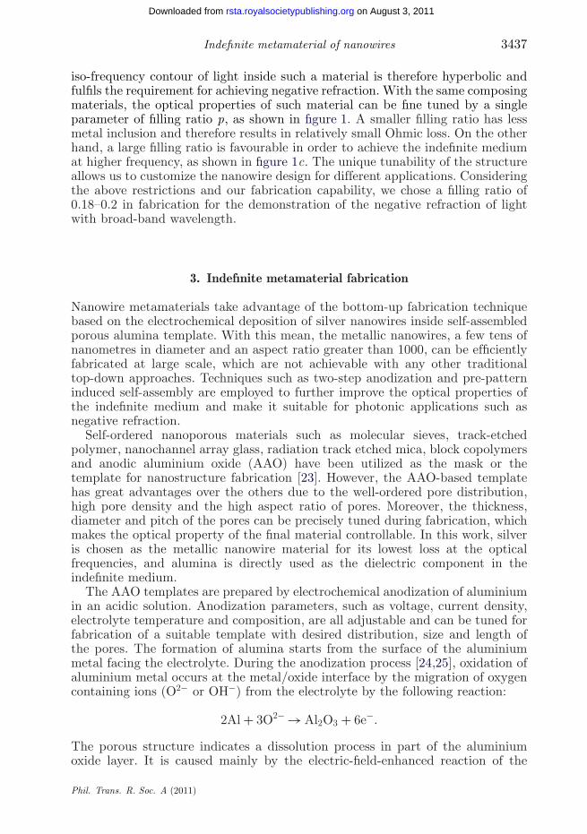
3438 J. Yao et al.
barrier layer
(a) (b)
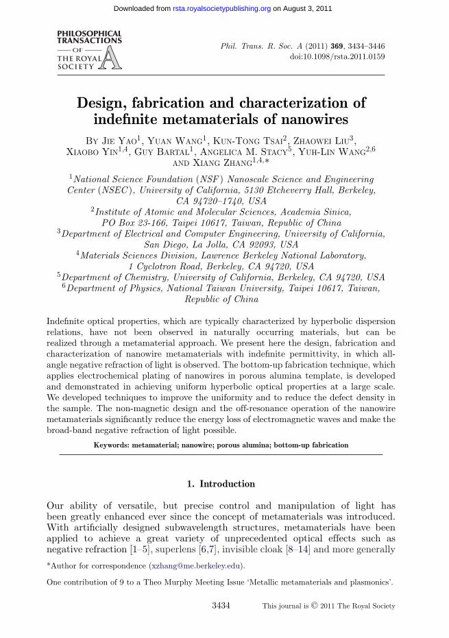
Figure 2. (a) Schematic of the vertical cross section of the porous alumina membrane formed ontop of an aluminium substrate. The curved layer at the bottom of each pore is the barrier layer.(b) Scanning electron microscope (SEM) image of the porous alumina template (top view). (Onlineversion in colour.)
formed oxide layer,
Al2O3 + 6H+ → 2Al3+(aq) + 3H2O.
The positions of the pores are induced by the concaves at the top surface of thealuminium before anodization. The oxidation of aluminium and the dissolutionof the oxide at the bottom of each pore are in equilibrium, hence a straight porecan be formed all the way into the metal layer (see figure 2). The formation ofpores also involves the interaction among them. The growth competition resultsin a self-organized process and adjusts the relative position of adjacent pores,thus an ordered hexagonal pore array can be formed [26].
Various acids can be used for aluminium anodization, and the geometric featureof pores varies significantly with the electrolytes used. Pore size and distancebetween pores can be further controlled using an applied voltage between theelectrodes. Generally speaking, they become larger as the anodization voltageincreases [27]. Here, we use 0.2 M oxalic acid in an ice water bath with 40 V bias,which achieves approximately 110 nm pitch and approximately 55 nm pore sizeover a large area with a regular pore shape. The filling ratio p is in the range0.18–0.2, as designed.
A better ordered nanopore array can be achieved using a two-step anodizationprocess [26], since the development of the nanopores in AAO templates is guidedby the appropriate texture of the surface at the initial stage of anodization. Highpurity aluminium foil (99.9995%, Alfa Aesar) was first mechanically polished anddegreased with acetone, then put into 0.2 M oxalic acid as an anode for the firstanodization step. The oxidized layer was then removed in a mixture of H3PO4and H2CrO4, leaving a regular array of dips on the metal surface due to theself-organizing mechanism. A second anodization is then applied to achieve AAOtemplates with the desired thickness. With the two-step method, pore sizes anddistances between the pores in the final template are much more controllable anduniform.
After the anodization process, the sample was immersed in a saturated solutionof Hg2Cl to remove the residual aluminium. The barrier layer at the bottom ofthe template was then removed in diluted H3PO4 at room temperature. After theremoval of a barrier layer, a silver seed layer was deposited (EB3, BOC Edwards)
Phil. Trans. R. Soc. A (2011)
on August 3, 2011rsta.royalsocietypublishing.orgDownloaded from
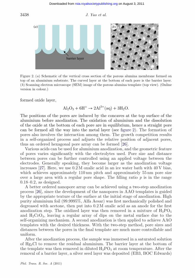
Indefinite metamaterial of nanowires 3439
(a) (b)
10 mm 10 mm
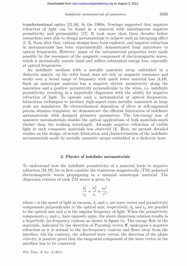
Figure 3. Cross-sectional view of an AAO template after the growth of a silver nanowire using theelectrochemical plating method. (a) The centre part of the sample. (b) Close to the edge of thesame sample in (a), the boundary between the nanowire filled and empty parts can be seen. Thenanowires grow faster at the edge than at the centre part, and overgrown silver forms a block ontop of the sample.
on top of the template as a cathode and silver nanowires were subsequentlyelectrochemically plated in the pores of an AAO template [28]. The electroplatingprocess was performed in the electrolyte containing AgNO3, nitric acid andl-tartaric acid.
Since the growth rate of nanowires is usually much faster close to the edge of thesample than in the centre [29], when the longer nanowires grow out of the pores,they will start to conglomerate at the surface and form a block of silver metal, asshown in figure 3. The overgrown silver on the surface was removed by mechanicalpolishing. The polishing process should not stop until all the short nanowires showup since the pores that are not fully filled act as strong optical scattering centres.
The bottom-up method using the self-organized porous template greatlyreduces the fabrication time and makes fine and high-aspect-ratio nanostructuresachievable. On the other hand, as shown in the previous example, materials madewith a bottom-up approach are usually not so uniform in the pore sizes, shapesand lattice regularity as those fabricated with top-down approaches, which makesthe fabrication of materials with good optical quality a great challenge. In orderto further improve the optical performance, it is critical to create pore arrayswith high uniformity.
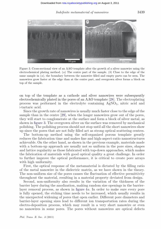
First, the optical response of the metamaterial is dictated by the filling ratioof the metal nanowire in the dielectric matrix, as we have shown in the theory.The non-uniform size of the pores causes the fluctuation of effective permittivitythroughout the material, resulting in a material property deviated from design.
Second, non-uniformity also results in the variation of the thickness of thebarrier layer during the anodization, making random size openings in the barrier-layer removal process, as shown in figure 4a. In order to make sure every poreis fully opened, the etching time needs to be increased, which usually results inthe unexpected widening of pores that open earlier. Different pore diameters andbarrier-layer opening sizes lead to different ion transportation rates during theelectro-deposition process, which may result in a very short nanowire or evenno nanowires in some pores. The pores without nanowires are optical defects
Phil. Trans. R. Soc. A (2011)
on August 3, 2011rsta.royalsocietypublishing.orgDownloaded from
3440 J. Yao et al.
(a) (b)
200 nm 200 nm 0
100 nm
Figure 4. Atomic force microscope images of the template bottom surface morphology after removalof the barrier layers. The two samples are fabricated using the two-step anodization approach. Firstanodization time is (a) 5 and (b) 24 h, respectively. (Online version in colour.)
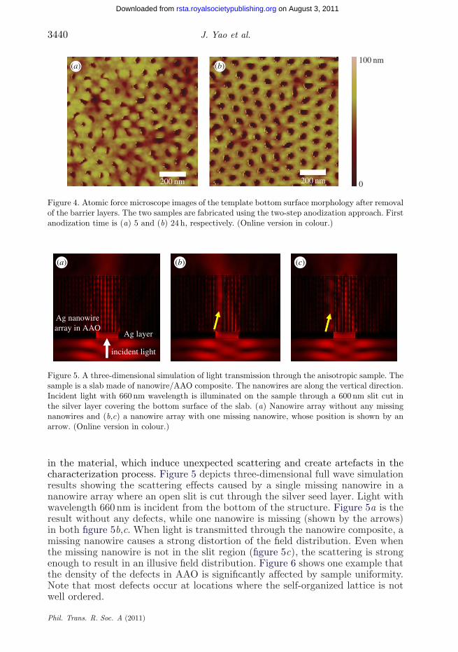
Ag nanowirearray in AAO
Ag layer
incident light
(a) (b) (c)
Figure 5. A three-dimensional simulation of light transmission through the anisotropic sample. Thesample is a slab made of nanowire/AAO composite. The nanowires are along the vertical direction.Incident light with 660 nm wavelength is illuminated on the sample through a 600 nm slit cut inthe silver layer covering the bottom surface of the slab. (a) Nanowire array without any missingnanowires and (b,c) a nanowire array with one missing nanowire, whose position is shown by anarrow. (Online version in colour.)
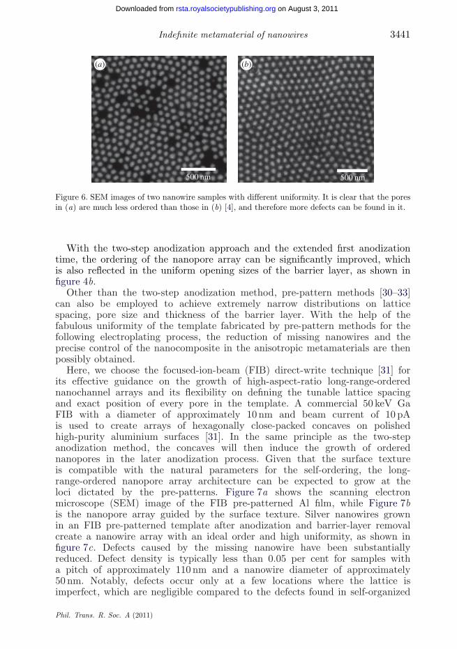
in the material, which induce unexpected scattering and create artefacts in thecharacterization process. Figure 5 depicts three-dimensional full wave simulationresults showing the scattering effects caused by a single missing nanowire in ananowire array where an open slit is cut through the silver seed layer. Light withwavelength 660 nm is incident from the bottom of the structure. Figure 5a is theresult without any defects, while one nanowire is missing (shown by the arrows)in both figure 5b,c. When light is transmitted through the nanowire composite, amissing nanowire causes a strong distortion of the field distribution. Even whenthe missing nanowire is not in the slit region (figure 5c), the scattering is strongenough to result in an illusive field distribution. Figure 6 shows one example thatthe density of the defects in AAO is significantly affected by sample uniformity.Note that most defects occur at locations where the self-organized lattice is notwell ordered.
Phil. Trans. R. Soc. A (2011)
on August 3, 2011rsta.royalsocietypublishing.orgDownloaded from
Indefinite metamaterial of nanowires 3441
(a) (b)
500 nm 500 nm
Figure 6. SEM images of two nanowire samples with different uniformity. It is clear that the poresin (a) are much less ordered than those in (b) [4], and therefore more defects can be found in it.
With the two-step anodization approach and the extended first anodizationtime, the ordering of the nanopore array can be significantly improved, whichis also reflected in the uniform opening sizes of the barrier layer, as shown infigure 4b.
Other than the two-step anodization method, pre-pattern methods [30–33]can also be employed to achieve extremely narrow distributions on latticespacing, pore size and thickness of the barrier layer. With the help of thefabulous uniformity of the template fabricated by pre-pattern methods for thefollowing electroplating process, the reduction of missing nanowires and theprecise control of the nanocomposite in the anisotropic metamaterials are thenpossibly obtained.
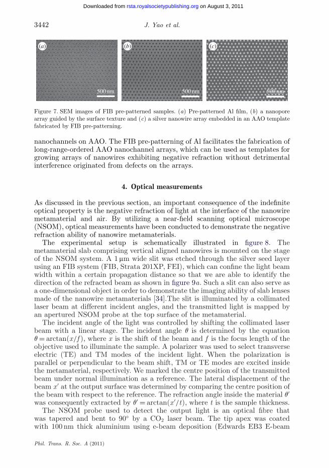
Here, we choose the focused-ion-beam (FIB) direct-write technique [31] forits effective guidance on the growth of high-aspect-ratio long-range-orderednanochannel arrays and its flexibility on defining the tunable lattice spacingand exact position of every pore in the template. A commercial 50 keV GaFIB with a diameter of approximately 10 nm and beam current of 10 pAis used to create arrays of hexagonally close-packed concaves on polishedhigh-purity aluminium surfaces [31]. In the same principle as the two-stepanodization method, the concaves will then induce the growth of orderednanopores in the later anodization process. Given that the surface textureis compatible with the natural parameters for the self-ordering, the long-range-ordered nanopore array architecture can be expected to grow at theloci dictated by the pre-patterns. Figure 7a shows the scanning electronmicroscope (SEM) image of the FIB pre-patterned Al film, while Figure 7bis the nanopore array guided by the surface texture. Silver nanowires grownin an FIB pre-patterned template after anodization and barrier-layer removalcreate a nanowire array with an ideal order and high uniformity, as shown infigure 7c. Defects caused by the missing nanowire have been substantiallyreduced. Defect density is typically less than 0.05 per cent for samples witha pitch of approximately 110 nm and a nanowire diameter of approximately50 nm. Notably, defects occur only at a few locations where the lattice isimperfect, which are negligible compared to the defects found in self-organized
Phil. Trans. R. Soc. A (2011)
on August 3, 2011rsta.royalsocietypublishing.orgDownloaded from
3442 J. Yao et al.
(a)
500 nm 500 nm 500 nm
(b) (c)
Figure 7. SEM images of FIB pre-patterned samples. (a) Pre-patterned Al film, (b) a nanoporearray guided by the surface texture and (c) a silver nanowire array embedded in an AAO templatefabricated by FIB pre-patterning.
nanochannels on AAO. The FIB pre-patterning of Al facilitates the fabrication oflong-range-ordered AAO nanochannel arrays, which can be used as templates forgrowing arrays of nanowires exhibiting negative refraction without detrimentalinterference originated from defects on the arrays.
4. Optical measurements
As discussed in the previous section, an important consequence of the indefiniteoptical property is the negative refraction of light at the interface of the nanowiremetamaterial and air. By utilizing a near-field scanning optical microscope(NSOM), optical measurements have been conducted to demonstrate the negativerefraction ability of nanowire metamaterials.
The experimental setup is schematically illustrated in figure 8. Themetamaterial slab comprising vertical aligned nanowires is mounted on the stageof the NSOM system. A 1 mm wide slit was etched through the silver seed layerusing an FIB system (FIB, Strata 201XP, FEI), which can confine the light beamwidth within a certain propagation distance so that we are able to identify thedirection of the refracted beam as shown in figure 9a. Such a slit can also serve asa one-dimensional object in order to demonstrate the imaging ability of slab lensesmade of the nanowire metamaterials [34].The slit is illuminated by a collimatedlaser beam at different incident angles, and the transmitted light is mapped byan apertured NSOM probe at the top surface of the metamaterial.
The incident angle of the light was controlled by shifting the collimated laserbeam with a linear stage. The incident angle q is determined by the equationq = arctan(x/f ), where x is the shift of the beam and f is the focus length of theobjective used to illuminate the sample. A polarizer was used to select transverseelectric (TE) and TM modes of the incident light. When the polarization isparallel or perpendicular to the beam shift, TM or TE modes are excited insidethe metamaterial, respectively. We marked the centre position of the transmittedbeam under normal illumination as a reference. The lateral displacement of thebeam x ′ at the output surface was determined by comparing the centre position ofthe beam with respect to the reference. The refraction angle inside the material q′was consequently extracted by q′ = arctan(x ′/t), where t is the sample thickness.
The NSOM probe used to detect the output light is an optical fibre thatwas tapered and bent to 90◦ by a CO2 laser beam. The tip apex was coatedwith 100 nm thick aluminium using e-beam deposition (Edwards EB3 E-beam
Phil. Trans. R. Soc. A (2011)
on August 3, 2011rsta.royalsocietypublishing.orgDownloaded from

Indefinite metamaterial of nanowires 3443
xyz-PZT
PMT
2 3
1
S
D
PO
BS
BS
lamp
CCD
ML
q1
AFM controller
Figure 8. Schematic setup for negative refraction in silver nanowire metamaterials (BS, beamsplitter; L, tube lens; M, mirror; O, objective; P, polarizer; xyz-PZT, piezo-scanner tunable inxyz directions; AFM, atomic force microscope; PMT, photomultiplier tube). The incident angle 1is tuned by adjusting the position of the laser diode (D) with a one-dimensional stage (S). Theinset illustrates a cross-sectional review of the light propagation of the TE mode (beam no. 2) andthe TM mode (beam no. 3) inside the metamaterial. (Online version in colour.)
0.5(a) (b)
TM
TE
0
Ag film Ag nanowiresin Al2O3 template
–0.5
–0.5–6 0
relative lateral displacement (µm)
sin
qsi
n q
6
0.5
0q
Figure 9. (a) Schematic picture of the light being negatively refracted at the air/metamaterialinterface. The light beam is narrowed by a slit cut through the silver seed layer. (b) Experimentalresults of NSOM detected output light beam location as the incident angle varies. Upper half,TM-polarized light; lower half, TE-polarized light. (Online version in colour.)
Phil. Trans. R. Soc. A (2011)
on August 3, 2011rsta.royalsocietypublishing.orgDownloaded from
3444 J. Yao et al.
Evaporator). Subsequently, the tip was milled using FIB milling (FEI Strata201 XP) to form a sub-100 nm aperture at the probe apex. When positioned inclose proximity to the sample surface with an atomic force microscope scanner(Bioscope, Digital Instruments), the light from the sample can be collected toform an image with subdiffraction resolution.
Figure 9a is a schematic showing the light path of a negatively refracted lightin our experiments. A slit is cut on the 250 nm thick silver film. A light beam at660 nm wavelength is transmitted through the slit and refracted to the negativedirection at the air/metamaterial interface. Figure 9b is the combined results of arefracted light spot for different incident angles. The horizontal axis represents thelateral displacement of the output light. The output beam of normally incidentlight is set as the reference point and marked as zero on the axis. The verticalaxes are the sines of various incident angles. When q is negative, normal refractiondictates that the output beam has a positive displacement. However, it is clearlyshown in the upper half of the figure that TM polarized light beams behave inthe opposite way, which shows a negative refraction. In a control experiment, TEpolarized light beams were positively refracted, as recorded in the lower half offigure 9b. Furthermore, negative refraction also occurs at the output interface ofthe sample, which leads to a focusing effect and forms an image of the slit at adistance from the output surface [34].
5. Conclusion
We have demonstrated the design, fabrication and optical characterization of anindefinite metamaterial composed of silver nanowires embedded in an aluminamatrix, achieving an effective indefinite property in permittivity. The majorchallenge of creating such metamaterials with good optical quality was overcomeby employing various techniques, including two-step anodization and the pre-patterning method, as well as parameter optimization to reduce the defectdensity. The approach is effective in producing high optical quality nanowiremetamaterials with designed parameters at large scale. The indefinite opticalproperties were characterized by an NSOM system, and the negative refractionability of the nanowire metamaterials was demonstrated. The experimentalresults in turn proved the validity of our theoretical framework and structuredesigns. An indefinite medium based on metallic nanowires has much lowermaterial losses than other negative index materials because of its non-magneticand off-resonance design. Such a bulk negative refractive material design hasopened new possibilities in the fields of nanoscale optical imaging and lithography.
This work was supported by the US Army Research Office (ARO) MURI program 50432-PH-MUR and partly by the National Science Council (NSC 95-3114-P-001-007-MY3) of Taiwan andAcademia Sinica of Taiwan.
References
1 Smith, D. R., Padilla, W. J., Vier, D. C., Nemat-Nasser, S. C. & Schultz, S. 2000 Compositemedium with simultaneously negative permeability and permittivity. Phys. Rev. Lett. 84,4184–4187. (doi:10.1103/PhysRevLett.84.4184)
Phil. Trans. R. Soc. A (2011)
on August 3, 2011rsta.royalsocietypublishing.orgDownloaded from
Indefinite metamaterial of nanowires 3445
2 Pendry, J. B. 2000 Negative refraction makes a perfect lens. Phys. Rev. Lett. 85, 3966–3969.(doi:10.1103/PhysRevLett.85.3966)
3 Shelby, R. A., Smith, D. R. & Schultz, S. 2001 Experimental verification of a negative index ofrefraction. Science 292, 77–79. (doi:10.1126/science.1058847)
4 Yao, J., Liu, Z., Liu, Y., Wang, Y., Sun, C., Bartal, G., Stacy, A. M. & Zhang, X. 2008Optical negative refraction in bulk metamaterials of nanowires. Science 321, 930. (doi:10.1126/science.1157566)
5 Valentine, J., Zhang, S., Zentgraf, T., Ulin-Avila, E., Genov, D. A., Bartal, G. & Zhang, X. 2008Three-dimensional optical metamaterial with a negative refractive index. Nature 455, 376–379.(doi:10.1038/nature07247)
6 Fang, N., Lee, H., Sun, C. & Zhang, X. 2005 Sub-diffraction-limited optical imaging with asilver superlens. Science 308, 534–537. (doi:10.1126/science.1108759)
7 Durant, S., Liu, Z., Steele, J. M. & Zhang, X. 2006 Theory of the transmission properties ofan optical far-field superlens for imaging beyond the diffraction limit. J. Opt. Soc. Am. B 23,2383–2392. (doi:10.1364/JOSAB.23.002383)
8 Schurig, D., Mock, J. J., Justice, B. J., Cummer, S. A., Pendry, J. B., Starr, A. F. & Smith,D. R. 2006 Metamaterial electromagnetic cloak at microwave frequencies. Science 314, 977–980.(doi:10.1126/science.1133628)
9 Cai, W., Chettiar, U. K., Kildishev, A. V. & Shalaev, V. M. 2007 Optical cloaking withmetamaterials. Nat. Photon 1, 224–227. (doi:10.1038/nphoton.2007.28)
10 Li, J. & Pendry, J. B. 2008 Hiding under the carpet: a new strategy for cloaking. Phys. Rev.Lett. 101, 203901. (doi:10.1103/PhysRevLett.101.203901)
11 Liu, R., Ji, C., Mock, J. J., Chin, J. Y., Cui, T. J. & Smith, D. R. 2009 Broadband ground-planecloak. Science 323, 366–369. (doi:10.1126/science.1166949)
12 Valentine, J., Li, J., Zentgraf, T., Bartal, G. & Zhang, X. 2009 An optical cloak made ofdielectrics. Nat. Mater. 8, 568–571. (doi:10.1038/nmat2461)
13 Ergin, T., Stenger, N., Brenner, P., Pendry, J. B. & Wegener, M. 2010 Three-dimensionalinvisibility cloak at optical wavelengths. Science 328, 337–339. (doi:10.1126/science.1186351)
14 Zhang, S., Genov, D. A., Sun, C. & Zhang, X. 2008 Cloaking of matter waves. Phys. Rev. Lett.100, 123002. (doi:10.1103/PhysRevLett.100.123002)
15 Pendry, J. B., Schurig, D. & Smith, D. R. 2006 Controlling electromagnetic fields. Science 312,1780–1782. (doi:10.1126/science.1125907)
16 Leonhardt, U. 2006 Optical conformal mapping. Science 312, 1777–1780. (doi:10.1126/science.1126493)
17 Veselago, V. G. 1968 The electrodynamics of substances with simultaneously negative valuesof 3 and m. Sov. Phys Usp. 10, 509. (doi:10.1070/PU1968v010n04ABEH003699)
18 Liu, Y., Bartal, G. & Zhang, X. 2008 All-angle negative refraction and imaging in a bulkmedium made of metallic nanowires in the visible region. Opt. Exp. 16, 15 439–15 448.(doi:10.1364/OE.16.015439)
19 Smith, D. R. & Schurig, D. 2003 Electromagnetic wave propagation in media with indefinitepermittivity and permeability tensors. Phys. Rev. Lett. 90, 077405. (doi:10.1103/PhysRevLett.90.077405)
20 Hornyak, G. L., Patrissi, C. J. & Martin, C. R. 1997 Fabrication, characterization, and opticalproperties of gold nanoparticle/porous alumina composites: the nonscattering Maxwell-Garnettlimit. J. Phys. Chem. B 101, 1548–1555. (doi:10.1021/jp962685o)
21 Johnson, P. B. & Christy, R. W. 1972 Optical constants of the noble metals. Phys. Rev. B6, 4370–4379. (doi:10.1103/PhysRevB.6.4370)
22 Podolskiy, V. A. & Narimanov, E. E. 2005 Strongly anisotropic waveguide as a nonmagneticleft-handed system. Phys. Rev. B 71, 201101. (doi:10.1103/PhysRevB.71.201101)
23 Martin, C. R. 1994 Nanomaterials: a membrane-based synthetic approach. Science 266, 1961–1966. (doi:10.1126/science.266.5193.1961)
24 Thompson, C. E. & Wood, G. C. 1983 Anodic films on aluminium. In Treatise on materialsscience and technology, pp. 205–329. New York, NY: Academic Press.
25 Li, F., Zhang, L. & Metzger, R. M. 1998 On the growth of highly ordered pores in anodizedaluminum oxide. Chem. Mater. 10, 2470–2480. (doi:10.1021/cm980163a)
Phil. Trans. R. Soc. A (2011)
on August 3, 2011rsta.royalsocietypublishing.orgDownloaded from

3446 J. Yao et al.
26 Masuda, H. & Fukuda, K. 1995 Ordered metal nanohole arrays made by a two-step replicationof honeycomb structures of anodic alumina. Science 268, 1466–1468. (doi:10.1126/science.268.5216.1466)
27 Li, A. P., Muller, F., Birner, A., Nielsch, K. & Gosele, U. 1998 Hexagonal pore arrays with a50–420 nm interpore distance formed by self-organization in anodic alumina. J. Appl. Phys. 84,6023–6026.
28 Lei, Y., Cai, W. & Wilde, G. 2007 Highly ordered nanostructures with tunable size, shape andproperties: a new way to surface nano-patterning using ultra-thin alumina masks. Progr. Mater.Sci. 52, 465–539. (doi:10.1016/j.pmatsci.2006.07.002)
29 Keyani, J. 2007 Electrodeposition and device incorporation of bismuth antimony nanowirearrays. PhD thesis, University of California Berkeley, USA.
30 Masuda, H., Yamada, H., Satoh, M., Asoh, H., Nakao, M. & Tamamura, T. 1997 Highlyordered nanochannel-array architecture in anodic alumina. Appl. Phys. Lett. 71, 2770–2772.(doi:10.1063/1.120128)
31 Liu, C. Y., Datta, A. & Wang, Y. L. 2001 Ordered anodic alumina nanochannels on focused-ion-beam-prepatterned aluminum surfaces. Appl. Phys. Lett. 78, 120–122. (doi:10.1063/1.1335543)
32 Krishnan, R. & Thompson, C. 2007 Monodomain high-aspect-ratio 2d and 3d ordered porousalumina structures with independently controlled pore spacing and diameter. Adv. Mater. 19,988–992. (doi:10.1002/adma.200601555)
33 Biring, S., Tsai, K., Sur, U. K. & Wang, Y. 2008 High speed fabrication of aluminumnanostructures with 10 nm spatial resolution by electrochemical replication. Nanotechnology19, 355302. (doi:10.1088/0957-4484/19/35/355302)
34 Yao, J., Tsai, K., Wang, Y., Liu, Z., Bartal, G., Wang, Y. & Zhang, X. 2009 Imaging visiblelight using anisotropic metamaterial slab lens. Opt. Exp. 17, 22 380–22 385. (doi:10.1364/OE.17.022380)
Phil. Trans. R. Soc. A (2011)
on August 3, 2011rsta.royalsocietypublishing.orgDownloaded from