Embed Size (px)
Citation preview

roberto sartori
Design, analysis and optimization of a dynamically
reconfigurable regenerative comparator for ultra-low power
6-bit TC-ADCs in 90nm CMOS technology

Design, analysis and optimization of a dynamically
reconfigurable regenerative comparator for
ultra-low power 6-bit TC-ADCs in 90nm CMOStechnology
roberto sartori
Supervisor Prof.ssa Maria Elena Valcher
Assistant Supervisor Dr.D. Juan A. Montiel-Nelson
October 2013

Roberto Sartori: Design, analysis and optimization of a dynamically recon-figurable regenerative comparator for ultra-low power 6-bit TC-ADCs in90nm CMOS technology, , © October 2013

Escuela de Ingeniería deTelecomunicación y Electrónica
Facultad de IngenieríaUniversidad de Las Palmas de
Gran Canaria
Dipartimento di Ingegneriadell’Informazione
Facoltà di IngegneriaUniversità degli Studi di Padova


"While the pessimists complain about the wind,and the optimists expect the wind to change,
we adjust the sails." — William Arthur Ward
To my family.

A B S T R A C T
Analog-to-Digital Converters (ADCs) have always been a topic of in-tense research in electronics since the advances in digital process-ing and storage technologies enabled for the pre-processing, post-processing and storage of analog signals as large streams of digitalvalues. Mixed signal integrated circuits, including data acquisitionand conversion, experienced a real revolution in terms of the numberof emerging applications in electronics and telecommunications.
Powerful processors appeared for mixed signal processing, allow-ing for longer word-length, higher operation frequencies and largermemory sizes. Research efforts were initially focused on increasingthe sampling rate and the resolution of the analog-to-digital anddigital-to-analog converters to meet real-time multimedia processingrequirements. Several acquisition methodologies and architectureswere presented to support a wide range of applications oriented toprocessing huge volumes of data [1].
However, nowadays there is a high number of emerging applica-tions where it is still necessary to collect and process analog data,but they are subject to strong energy consumption restrictions. Mo-bile phones containing gyroscopes and accelerometers among othersensor assisted Global Positioning System (GPS) navigation applica-tions, sensor networks supported by small batteries, or medical aidsusing remote sensing battery-less are typical ultra-low power appli-cations requiring Analog-to-Digital Converter (ADC) subsystems. Theconversion rate and resolution specifications are less restrictive thanthe power consumption restrictions in these applications. Typically,ultra-low power requirements must be met, but just some few sam-ples or kilo-samples per second are needed for 4-8 bit resolutions.Therefore, among all ADC architectures in literature, the SuccessiveApproximation Register (SAR) and SD converters are the more suit-able architectures [2] for this purpose.
It is well known that SAR architectures are preferable in terms ofarea and power consumption in comparison with the other topologies[3] at medium and low conversion rates. Furthermore, due to the factthat high performance technologies are mainly focused on reducingthe delay while maintaining low power consumption in the digitalcircuitry, the use of recent technlogies in ADC design is more effectiveas greater is the digital section in comparison with its analog one [4].In this sense, several approaches have been presented to optimize thedigital controller reducing the power and increasing the conversionspeed on SAR ADC architectures by using comparator-based binarysearch [5, 6] and asynchronous controllers [7, 8, 9]. In a Comparator-
ix
based Asynchronous Binary Search (CABS), the need for digital-to-analog conversion and digital controllers is completely removed byusing a binary tree of comparators with built-in thresholds whichare triggered to run the successive approximation algorithm [5]. Butthe circuit complexity of this approach follows the same exponentialgrowth than flash ADCs.
Recently, a novel ADC architecture named Threshold-ConfiguringADC (TC-ADC) was introduced [10]. TC-ADC is based on a single com-parator and a programable array of transistors that allow to imple-ment the ADC and Digital-to-Analog Converter (DAC) functionalities[11]. The TC-ADC authors demonstrate the usefulness of this new ar-chitecture when low power consumption is required at medium/lowconversion rates.
In this work the threshold configurable regenerative comparatoron which TC-ADCs are based is optimized to further reduce the powerconsumption for use in battery-less biomedical sensor applications.Moreover, the effect of device mismatches on the offset, gain andlinearity errors of the ADC is analyzed by means of Monte Carlosimulations. This optimized comparator reduces the power consump-tion from 13µW to 3µW in the more power hungry section of theTC-ADC (65% of the overall TC-ADC power is dissipated in the re-generative comparator), while maintaining the same full scale range.The optimized comparator achieves also better performance (about50% improvement) in terms of offset, gain and non-linearity errorswhen matched devices are given. In the presence of device mismatchjust the gain error shows a significative improvement, although non-linearity error analysis indicates higher simmetry and predictabil-ity which can be further exploited to reduce the complexity of non-linearity cancellation circuits required for higher resolution applica-tions.
R E S U M E N
En este trabajo se optimiza el comparador regenerativo configurablede umbral en lo que el Threshold-Configuring SAR-ADC se basa parareducir aún más el consumo de energía, en aplicaciones de sensoresbiomédicos sin batería [1]. Por otra parte, el efecto de la dispersiónde proceso de los dispositivos en características del conversor como eloffset, la ganancia y los errores de linealidad del ADC se han de anali-zar de forma cualitativa y cuantitativa por medio de simulaciones deMonte Carlo. Resultados previos muestran que estos comparadores
x
optimizados permiten reducir el consumo de energía de 13µW hasta3µW manteniendo constante el mismo fondo de escala.
En presencia de la dispersión de proceso “device mismatch”, losmismos resultados previos muestran que sólo el error de gananciamuestra una mejora significativa, aunque el análisis de error de nolinealidad indica una mayor simetría y la previsibilidad. Estas dos ca-racterísticas pueden aprovecharse más para reducir la complejidad delos circuitos de cancelación de no linealidad requerida para aquellasaplicaciones de mayor resolución [12].
Por todo lo anterior, es objetivo de este trabajo obtener las rela-ciones cualitativas y cuantitativas entre dimensiones de dispositivos,potencia consumida, fondo de escala, errores de linealidad, offsety ganancia del conversor ADC basado en un comparador de um-bral reconfigurable y regenerativo como el referenciado en [13]. Es-tas relaciones permiten dimensionar el comparador para una aplica-cion de ultra bajo consumo de potencia. El proceso tecnologico esde UMC, Complementary Metal-Oxide-Semiconductor (CMOS) 90nm“Standard Process 1.0V CMOS 1P9M”.
C O M P E N D I O
Il presente studio mira ad ottimizzare il comparatore di soglia di ten-sione regenerativo riconfigurabile su cui si basa il Threshold-ConfiguringSAR ADC, al fine di ridurre ulteriormente il consumo di energia in ap-plicazioni quali sensori biomedici senza batteria. Vengono inoltre ana-lizzati in forma qualitativa e quantitativa gli effetti della dispersionedi processo dei dispositivi che costituiscono il convertitore, l’offset,il guadagno e gli errori di linearità del ADC, attraverso simulazioniMonte Carlo. Risultati precedenti mostrano come questi comparatoriottimizzati permettano di ridurre il consumo di energia da 13µW a3µW mantenendo costante il fondo scala.
L’obiettivo finale è dunque quello di ottenere le relazioni qualitativee quantitative tra le dimensioni dei dispositivi, la potenza dissipata,il fondo di scala, gli errori di linearità, l’offset e il guadagno del ADC
basato sul comparatore di soglia di tensione riconfigurabile e rigene-rativo presentato in [13]. Tali relazioni permettono di dimensionareil comparatore per applicazioni ad ultra basso consumo di potenza.Il processo tecnologico con cui vengono sviluppate le simulazioni èUMC, CMOS 90nm “Standard Process 1.0V CMOS 1P9M”.
xi

C O N T E N T S
Abstract . . . . . . . . . . . . . . . . . . . . . . . . . . . . . . ixList of Figures . . . . . . . . . . . . . . . . . . . . . . . . . . xvList of Tables . . . . . . . . . . . . . . . . . . . . . . . . . . . xxListings . . . . . . . . . . . . . . . . . . . . . . . . . . . . . . xxi
i ultra-low power adc architectures . . . . . . 1
1 introduction . . . . . . . . . . . . . . . . . . . . . . . 3
1.1 Basic A/D converter function . . . . . . . . . . . . 3
1.1.1 Conversion systems . . . . . . . . . . . . . 4
1.2 Specifications of converters . . . . . . . . . . . . . 4
1.2.1 Absolute accuracy . . . . . . . . . . . . . . 5
1.2.2 Relative accuracy . . . . . . . . . . . . . . . 5
1.2.3 Differential nonlinearity . . . . . . . . . . . 6
1.2.4 Offset . . . . . . . . . . . . . . . . . . . . . . 7
1.2.5 Signal-to-Noise Ratio . . . . . . . . . . . . . 7
1.2.6 Effective Number of Bits . . . . . . . . . . . 8
1.2.7 Figure of Merit . . . . . . . . . . . . . . . . 8
2 a/d converters . . . . . . . . . . . . . . . . . . . . . 9
2.1 Low-power ADC architectures . . . . . . . . . . . 13
2.1.1 Nyquist-rate ADCs . . . . . . . . . . . . . . 14
2.1.2 Oversampled ADCs . . . . . . . . . . . . . 17
2.2 Successive Approximation Register ADCs . . . . . 19
2.2.1 Low-power SAR ADCs . . . . . . . . . . . 21
2.3 Comparator-Based Binary Search ADCs . . . . . . 22
2.3.1 SAR ADCs using CC . . . . . . . . . . . . . 24
2.4 Threshold-Configuring ADCs . . . . . . . . . . . 25
2.4.1 TC-ADC Principle of Operation . . . . . . 25
2.4.2 Architectural Details . . . . . . . . . . . . . 27
2.4.3 Circuit Implementation . . . . . . . . . . . 28
ii an ultra-low power comparator . . . . . . . . 31
3 threshold-configurable comparator . . . . . 33
3.1 Basic Operation . . . . . . . . . . . . . . . . . . . . 34
3.2 Threshold Generation . . . . . . . . . . . . . . . . 35
3.3 Design Methodology . . . . . . . . . . . . . . . . . 36
4 design specification requirements . . . . . . . 39
4.1 TC-Comparator power consumption vs full scale . . 39
4.1.1 Results . . . . . . . . . . . . . . . . . . . . . 41
4.2 RFID Reader radiated power vs distance . . . . . . . 44
iii sizing and optimization . . . . . . . . . . . . . . 47
5 simulation environment set-up . . . . . . . . . 49
xiii
xiv contents
5.1 HSPICE Environment Structure . . . . . . . . . . . 49
5.1.1 Files Hierarchy . . . . . . . . . . . . . . . . 51
5.2 Simulation Setup . . . . . . . . . . . . . . . . . . . 52
6 sizing for ultra-low power and fs operation 55
6.1 Characteristics of CMOS Devices . . . . . . . . . . 55
6.1.1 Threshold voltage . . . . . . . . . . . . . . . 55
6.1.2 Maximum drain-source Currents . . . . . . 56
6.1.3 Parasitic Capacitance and on-state Resistance 56
6.1.4 Transconductance and gain-bandwidth . . 57
6.2 UMC CMOS 90nm Process Characteristics . . . . 57
6.2.1 Electrical parameters . . . . . . . . . . . . . 59
6.2.2 Model fitting accuracy . . . . . . . . . . . . 62
7 optimization for linearity improvement . . . 63
7.1 Analysis Methodology . . . . . . . . . . . . . . . . 63
7.1.1 Optimization analysis by Bisection method 65
7.2 Design restrictions Achievement . . . . . . . . . . 66
7.3 NonLinearity Analysis: DNL and INL errors . . . 67
8 mismatch analysis . . . . . . . . . . . . . . . . . . . 69
8.1 Mismatch optimization through DNL analysis . . 69
9 results . . . . . . . . . . . . . . . . . . . . . . . . . . . 71
9.1 Optimization Results – scanning method . . . . . . 77
9.2 Reference Values – scanning method . . . . . . . . 92
9.3 Mismatch Results – Monte Carlo simulation . . . . 108
9.4 Conclusions . . . . . . . . . . . . . . . . . . . . . . 135
iv appendix . . . . . . . . . . . . . . . . . . . . . . . . . 137
a appendix . . . . . . . . . . . . . . . . . . . . . . . . . . 139
a.1 The SAR Algorithm . . . . . . . . . . . . . . . . . . 139
a.2 Nyquist sampling condition . . . . . . . . . . . . . 140
a.3 Nyquist frequency . . . . . . . . . . . . . . . . . . 141
a.4 Corner of Process . . . . . . . . . . . . . . . . . . . 141
a.5 Bisection Methodology in HSPICE . . . . . . . . . 143
a.6 tcadc file code . . . . . . . . . . . . . . . . . . . . . 147
a.7 Optimization models files code . . . . . . . . . . . 158
a.7.1 Simulation script for sheader.sp file . . . . 158
a.7.2 Simulation script for oheader.sp file . . . . 164
a.7.3 Simulation script for mheader file . . . . . . 169
a.8 circuits.inc file code . . . . . . . . . . . . . . . . 181
bibliography . . . . . . . . . . . . . . . . . . . . . . . . . 185
Acknowledgments . . . . . . . . . . . . . . . . . . . . . . . 191
L I S T O F F I G U R E S
Figure 1.1 Block diagram of an ADC . . . . . . . . . 3
Figure 1.2 A/D converter system . . . . . . . . . . . 4
Figure 1.3 Ideal converter . . . . . . . . . . . . . . . . 5
Figure 1.4 Transfer curve of a 4-bit ADC . . . . . . . 7
Figure 2.1 Full-flash ADC architecture . . . . . . . . 9
Figure 2.2 Sub ranging converter architecture . . . . 10
Figure 2.3 Dual slope ADC architecture . . . . . . . 12
Figure 2.4 Pipeline converter architecture . . . . . . 15
Figure 2.5 Low-power pipeline SC ADC . . . . . . . 15
Figure 2.6 Block diagram of an SAR ADC . . . . . . 16
Figure 2.7 3-bit SA ADC . . . . . . . . . . . . . . . . 17
Figure 2.8 Sigma-delta ADC architecture . . . . . . . 18
Figure 2.9 Incremental ADC architecture . . . . . . . 19
Figure 2.10 SAR ADC architecture . . . . . . . . . . . 20
Figure 2.11 Low-power DAC architecture . . . . . . . 22
Figure 2.12 Operating principle of a CABS ADC, shownfor a 3-bit ADC with 0.3 input on a 0 to range(dashed lines indicate active path) . . . . 23
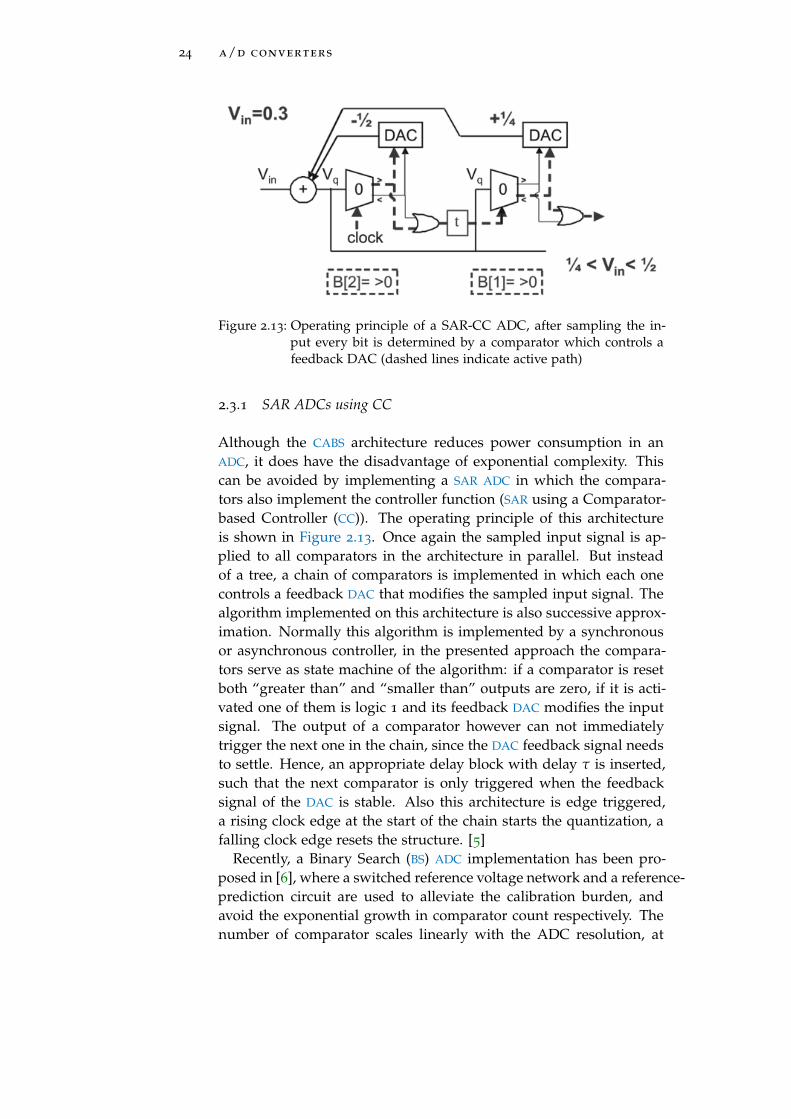
Figure 2.13 Operating principle of a SAR-CC ADC, aftersampling the input every bit is determined bya comparator which controls a feedback DAC(dashed lines indicate active path) . . . . 24
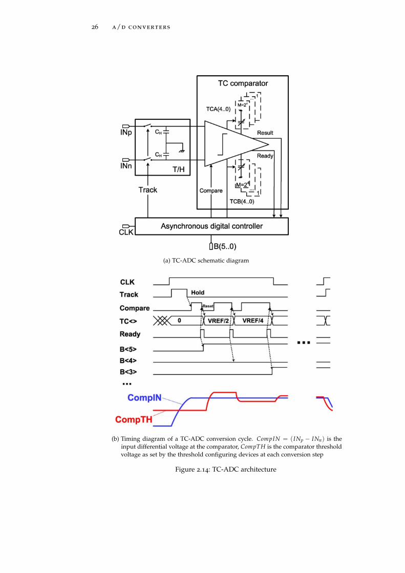
Figure 2.14 TC-ADC architecture . . . . . . . . . . . . 26
Figure 2.15 Simplified block diagram of the digital con-troller . . . . . . . . . . . . . . . . . . . . . 29
Figure 3.1 Simplified Threshold Configuring regenerativeComparator . . . . . . . . . . . . . . . . . 33
Figure 4.1 Qualitative output of scanning optimization method 40
Figure 4.2 vid values generation for scanning . . . . 41
Figure 4.3 Inner resistance Model for the comparator leftbranch . . . . . . . . . . . . . . . . . . . . 42
Figure 4.4 TC-Comparator concentrated parameters Model 42
Figure 4.5 Qualitative analysis of the current i flowingthrough the comparator branches . . . . . 43
Figure 4.6 Illustration of the Friis Transmission Formula 44
Figure 4.7 Available power at the output of the receivingantenna as a function of the distance . . . 45
Figure 5.1 HSPICE Environment structure . . . . . . 50
Figure 5.2 Netlist structure . . . . . . . . . . . . . . . 50
Figure 5.3 Ideal Equilibrium Point Inputs-Loads in a TC-Comparator . . . . . . . . . . . . . . . . . 52
xv
xvi List of Figures
Figure 5.4 Imbalance between Input and Load due to ther-mal noise . . . . . . . . . . . . . . . . . . . 53
Figure 5.5 Threshold Voltage Detection for a TC-Comparator 54
Figure 6.1 Origin of MOSFET Internal Resistance . . 57
Figure 7.1 Power consumption and FS trends over time fora TC-Comparator . . . . . . . . . . . . . . 64
Figure 7.2 Stable region for Output values detection 65
Figure 7.3 Qualitative plot of non-linear relationship be-tween Input voltage and Output digital codefor a TC-Comparator . . . . . . . . . . . . 68
Figure 8.1 Qualitative plot of INL errors for each digitalcode generated through Monte Carlo simula-tions . . . . . . . . . . . . . . . . . . . . . . 70
Figure 9.1 Non-linearity plots . . . . . . . . . . . . . 74
Figure 9.2 INL plots using mismatched devices: (a) and(b) are 3D-plots, and (c) and (d) are the corre-sponding 2D-plots, for the reference and poweroptimized comparators . . . . . . . . . . . 75
Figure 9.3 INL plots using mismatched devices: (a) and(b) are 3D-plots, and (c) and (d) are the corre-sponding 2D-plots, for the reference and poweroptimized comparators . . . . . . . . . . . 76
Figure 9.4 Vth Determination Conditions 1 - scanning mode,opt.val. . . . . . . . . . . . . . . . . . . . . . 77
Figure 9.5 Vth Determination Conditions 2 - scanning mode,opt.val. . . . . . . . . . . . . . . . . . . . . . 77
Figure 9.6 Average Power Consumption vs Vth - scanningmode, opt.val. . . . . . . . . . . . . . . . . . 78
Figure 9.7 RMS Power Consumption vs Vth - scanning mode,opt.val. . . . . . . . . . . . . . . . . . . . . . 78
Figure 9.8 Int Power Consumption vs Vth - scanning mode,opt.val. . . . . . . . . . . . . . . . . . . . . . 79
Figure 9.9 Average Current vs Vth 1 - scanning mode, opt.val. 79
Figure 9.10 Average Current vs Vth 2 - scanning mode, opt.val. 80
Figure 9.11 Average Current vs Vth 3 - scanning mode, opt.val. 80
Figure 9.12 Average Current vs Vth 4 - scanning mode, opt.val. 81
Figure 9.13 Average Current vs Vth 5 - scanning mode, opt.val. 81
Figure 9.14 Average Current vs Vth 6 - scanning mode, opt.val. 82
Figure 9.15 Average Current vs Vth 7 - scanning mode, opt.val. 82
Figure 9.16 Average Current vs Vth 8 - scanning mode, opt.val. 83
Figure 9.17 RMS Current vs Vth 1 - scanning mode, opt.val. 83
Figure 9.18 RMS Current vs Vth 2 - scanning mode, opt.val. 84
Figure 9.19 RMS Current vs Vth 3 - scanning mode, opt.val. 84
Figure 9.20 Int Current vs Vth 1 - scanning mode, opt.val. 85
Figure 9.21 Int Current vs Vth 2 - scanning mode, opt.val. 85
Figure 9.22 Int Current vs Vth 3 - scanning mode, opt.val. 86

List of Figures xvii
Figure 9.23 Average Current vs Vth 1 - scanning mode, opt.val. 86
Figure 9.24 Average Current vs Vth 2 - scanning mode, opt.val. 87
Figure 9.25 RMS Current vs Vth 4 - scanning mode, opt.val. 87
Figure 9.26 RMS Current vs Vth 5 - scanning mode, opt.val. 88
Figure 9.27 RMS Current vs Vth 6 - scanning mode, opt.val. 88
Figure 9.28 Int Current vs Vth 4 - scanning mode, opt.val. 89
Figure 9.29 Int Current vs Vth 5 - scanning mode, opt.val. 89
Figure 9.30 Int Current vs Vth 6 - scanning mode, opt.val. 90
Figure 9.31 Time Delay for Decode vs Vth 1 - scanning mode,opt.val. . . . . . . . . . . . . . . . . . . . . . 90
Figure 9.32 Time Delay for Decode vs Vth 2 - scanning mode,opt.val. . . . . . . . . . . . . . . . . . . . . . 91
Figure 9.33 Time Delay for Decode vs Vth 3 - scanning mode,opt.val. . . . . . . . . . . . . . . . . . . . . . 91
Figure 9.34 Vth Determination Conditions 1 - scanning mode,ref.val. . . . . . . . . . . . . . . . . . . . . . 93
Figure 9.35 Vth Determination Conditions 2 - scanning mode,ref.val. . . . . . . . . . . . . . . . . . . . . . 93
Figure 9.36 Average Power Consumption vs Vth - scanningmode, ref.val. . . . . . . . . . . . . . . . . . 94
Figure 9.37 RMS Power Consumption vs Vth - scanning mode,ref.val. . . . . . . . . . . . . . . . . . . . . . 94
Figure 9.38 Int Power Consumption vs Vth - scanning mode,ref.val. . . . . . . . . . . . . . . . . . . . . . 95
Figure 9.39 Average Current vs Vth 1 - scanning mode, ref.val. 95
Figure 9.40 Average Current vs Vth 2 - scanning mode, ref.val. 96
Figure 9.41 Average Current vs Vth 3 - scanning mode, ref.val. 96
Figure 9.42 Average Current vs Vth 4 - scanning mode, ref.val. 97
Figure 9.43 Average Current vs Vth 5 - scanning mode, ref.val. 97
Figure 9.44 Average Current vs Vth 6 - scanning mode, ref.val. 98
Figure 9.45 Average Current vs Vth 7 - scanning mode, ref.val. 98
Figure 9.46 Average Current vs Vth 8 - scanning mode, ref.val. 99
Figure 9.47 RMS Current vs Vth 1 - scanning mode, ref.val. 99
Figure 9.48 RMS Current vs Vth 2 - scanning mode, ref.val.100
Figure 9.49 RMS Current vs Vth 3 - scanning mode, ref.val.100
Figure 9.50 Int Current vs Vth 1 - scanning mode, ref.val. 101
Figure 9.51 Int Current vs Vth 2 - scanning mode, ref.val. 101
Figure 9.52 Int Current vs Vth 3 - scanning mode, ref.val. 102
Figure 9.53 Average Current vs Vth 1 - scanning mode, ref.val.102
Figure 9.54 Average Current vs Vth 2 - scanning mode, ref.val.103
Figure 9.55 RMS Current vs Vth 4 - scanning mode, ref.val.103
Figure 9.56 RMS Current vs Vth 5 - scanning mode, ref.val.104
Figure 9.57 RMS Current vs Vth 6 - scanning mode, ref.val.104
Figure 9.58 Int Current vs Vth 4 - scanning mode, ref.val. 105
Figure 9.59 Int Current vs Vth 5 - scanning mode, ref.val. 105
Figure 9.60 Int Current vs Vth 6 - scanning mode, ref.val. 106
xviii List of Figures
Figure 9.61 Time Delay for Decode vs Vth 1 - scanning mode,ref.val. . . . . . . . . . . . . . . . . . . . . . 106
Figure 9.62 Time Delay for Decode vs Vth 2 - scanning mode,ref.val. . . . . . . . . . . . . . . . . . . . . . 107
Figure 9.63 Time Delay for Decode vs Vth 3 - scanning mode,ref.val. . . . . . . . . . . . . . . . . . . . . . 107
Figure 9.64 Slope - mismatch, MonteCarlo EndPoint method109
Figure 9.65 Offset - mismatch, MonteCarlo EndPoint method109
Figure 9.66 Offset Error (LSB) - mismatch, MonteCarlo End-Point method . . . . . . . . . . . . . . . . . 110
Figure 9.67 Gain Error % - mismatch, MonteCarlo EndPointmethod . . . . . . . . . . . . . . . . . . . . . 110
Figure 9.68 Min INL (LSB) - mismatch, MonteCarlo EndPointmethod . . . . . . . . . . . . . . . . . . . . . 111
Figure 9.69 Max INL (LSB) - mismatch, MonteCarlo EndPointmethod . . . . . . . . . . . . . . . . . . . . . 111
Figure 9.70 Median INL (LSB) - mismatch, MonteCarlo End-Point method . . . . . . . . . . . . . . . . . 112
Figure 9.71 Mean INL (LSB) - mismatch, MonteCarlo End-Point method . . . . . . . . . . . . . . . . . 112
Figure 9.72 Standard Deviation INL (LSB) - mismatch, Mon-teCarlo EndPoint method . . . . . . . . . . . 113
Figure 9.73 Sum INL (LSB) - mismatch, MonteCarlo EndPointmethod . . . . . . . . . . . . . . . . . . . . . 113
Figure 9.74 Sum Sq INL (LSB) - mismatch, MonteCarlo End-Point method . . . . . . . . . . . . . . . . . 114
Figure 9.75 Min DNL (LSB) - mismatch, MonteCarlo End-Point method . . . . . . . . . . . . . . . . . 114
Figure 9.76 Max DNL (LSB) - mismatch, MonteCarlo End-Point method . . . . . . . . . . . . . . . . . 115
Figure 9.77 Median DNL (LSB) - mismatch, MonteCarlo End-Point method . . . . . . . . . . . . . . . . . 115
Figure 9.78 Mean DNL (LSB) - mismatch, MonteCarlo End-Point method . . . . . . . . . . . . . . . . . 116
Figure 9.79 Sum DNL (LSB) - mismatch, MonteCarlo End-Point method . . . . . . . . . . . . . . . . . 116
Figure 9.80 Slope - mismatch, MonteCarlo LSE method . 117
Figure 9.81 Offset - mismatch, MonteCarlo LSE method 117
Figure 9.82 Offset Error (LSB) - mismatch, MonteCarlo LSEmethod . . . . . . . . . . . . . . . . . . . . . 118
Figure 9.83 Gain Error % - mismatch, MonteCarlo LSE method118
Figure 9.84 Min INL (LSB) - mismatch, MonteCarlo LSE method119
Figure 9.85 Max INL (LSB) - mismatch, MonteCarlo LSE method119
Figure 9.86 Median INL (LSB) - mismatch, MonteCarlo LSEmethod . . . . . . . . . . . . . . . . . . . . . 120
List of Figures xix
Figure 9.87 Mean INL (LSB) - mismatch, MonteCarlo LSEmethod . . . . . . . . . . . . . . . . . . . . . 120
Figure 9.88 Standard Deviation INL (LSB) - mismatch, Mon-teCarlo LSE method . . . . . . . . . . . . . . 121
Figure 9.89 Sum INL (LSB) - mismatch, MonteCarlo LSE method121
Figure 9.90 Sum Sq INL (LSB) - mismatch, MonteCarlo LSEmethod . . . . . . . . . . . . . . . . . . . . . 122
Figure 9.91 Min DNL (LSB) - mismatch, MonteCarlo LSE method122
Figure 9.92 Max DNL (LSB) - mismatch, MonteCarlo LSEmethod . . . . . . . . . . . . . . . . . . . . . 123
Figure 9.93 Median DNL (LSB) - mismatch, MonteCarlo LSEmethod . . . . . . . . . . . . . . . . . . . . . 123
Figure 9.94 Mean DNL (LSB) - mismatch, MonteCarlo LSEmethod . . . . . . . . . . . . . . . . . . . . . 124
Figure 9.95 Standard Deviation DNL (LSB) - mismatch, Mon-teCarlo LSE method . . . . . . . . . . . . . . 124
Figure 9.96 Sum DNL (LSB) - mismatch, MonteCarlo LSEmethod . . . . . . . . . . . . . . . . . . . . . 125
Figure 9.97 Sum Sq DNL (LSB) - mismatch, MonteCarlo LSEmethod . . . . . . . . . . . . . . . . . . . . . 125
Figure 9.98 Slope - mismatch, MonteCarlo EndPoint&LSE method126
Figure 9.99 Offset - mismatch, MonteCarlo EndPoint&LSE method126
Figure 9.100 Offset Error (LSB) - mismatch, MonteCarlo End-Point&LSE method . . . . . . . . . . . . . . 127
Figure 9.101 Gain Error % - mismatch, MonteCarlo EndPoint&LSEmethod . . . . . . . . . . . . . . . . . . . . . 127
Figure 9.102 Min INL (LSB) - mismatch, MonteCarlo EndPoint&LSEmethod . . . . . . . . . . . . . . . . . . . . . 128
Figure 9.103 Max INL (LSB) - mismatch, MonteCarlo EndPoint&LSEmethod . . . . . . . . . . . . . . . . . . . . . 128
Figure 9.104 Median INL (LSB) - mismatch, MonteCarlo End-Point&LSE method . . . . . . . . . . . . . . 129
Figure 9.105 Mean INL (LSB) - mismatch, MonteCarlo End-Point&LSE method . . . . . . . . . . . . . . 129
Figure 9.106 Standard Deviation INL (LSB) - mismatch, Mon-teCarlo EndPoint&LSE method . . . . . . . 130
Figure 9.107 Sum INL (LSB) - mismatch, MonteCarlo EndPoint&LSEmethod . . . . . . . . . . . . . . . . . . . . . 130
Figure 9.108 Sum Sq INL (LSB) - mismatch, MonteCarlo End-Point&LSE method . . . . . . . . . . . . . . 131
Figure 9.109 Min DNL (LSB) - mismatch, MonteCarlo End-Point&LSE method . . . . . . . . . . . . . . 131
Figure 9.110 Max DNL (LSB) - mismatch, MonteCarlo End-Point&LSE method . . . . . . . . . . . . . . 132
Figure 9.111 Mean DNL (LSB) - mismatch, MonteCarlo End-Point&LSE method . . . . . . . . . . . . . . 132

Figure 9.112 Standard Deviation DNL (LSB) - mismatch, Mon-teCarlo EndPoint&LSE method . . . . . . . 133
Figure 9.113 Sum DNL (LSB) - mismatch, MonteCarlo End-Point&LSE method . . . . . . . . . . . . . . 133
Figure 9.114 Sum Sq DNL (LSB) - mismatch, MonteCarlo End-Point&LSE method . . . . . . . . . . . . . . 134
Figure A.1 Successive Approximation ADC Block Diagram139
Figure A.2 Process corners in PMOS/NMOS fabricationparameters . . . . . . . . . . . . . . . . . . 142
Figure A.3 Bisection Example for Three Iterations . . 144
L I S T O F TA B L E S
Table 2.1 Classification of Nyquist-rate ADCs( T = clock period, N = resolution in bits) 14
Table 4.1 Size vs Power consumption vs Full-Scale relation-ships . . . . . . . . . . . . . . . . . . . . . 41
Table 6.1 Geometry range for UMC CMOS 90nm Pro-cess Model . . . . . . . . . . . . . . . . . . 58
Table 6.2 Voltage range for UMC CMOS 90nm ProcessModel . . . . . . . . . . . . . . . . . . . . 58
Table 6.3 Temperature range for UMC CMOS 90nm Pro-cess Model . . . . . . . . . . . . . . . . . . 58
Table 6.4 Electrical parameters for NMOS UMC 90nmProcess Model . . . . . . . . . . . . . . . . 60
Table 6.5 Electrical parameters for PMOS UMC 90nm Pro-cess Model . . . . . . . . . . . . . . . . . . 61
Table 7.1 Impact of device sizing in the performance ofthe threshold configuring comparator . . 66
Table 9.1 Device sizing parameters for reference (REF)and optimized (OPT) comparators . . . . 72
Table 9.2 Obtained performance for reference (REF) andoptimized (OPT) comparators, without devicemismatch . . . . . . . . . . . . . . . . . . . 72
Table 9.3 Obtained performance for reference (REF) andoptimized (OPT) comparators, with device mis-match . . . . . . . . . . . . . . . . . . . . . 72
Table A.1 Device name reference for HSPICE codes 181
xx

Listings xxi
L I S T I N G S
Listing 1 tcadc . . . . . . . . . . . . . . . . . . . . . 147
Listing 2 sheader.sp - Scanning optimization mode 158
Listing 3 oheader.sp - Bisection optimization mode 164
Listing 4 mheader.sp - Monte Carlo optimization mode169
Listing 5 circuits.inc . . . . . . . . . . . . . . . . 181

A C R O N Y M S
ADC Analog-to-Digital Converter
AVG AVeRage
BS Binary Search
CABS Comparator-based Asynchronous Binary Search
CC Comparator-based Controller
CMOS Complementary Metal-Oxide-Semiconductor
CR Charge-Redistribution
CS Charge-Sharing
CtrlTC Threshold Configuration control
DAC Digital-to-Analog Converter
DNL Differential NonLinearity
DoE Design-of-Experiments
ENOB Effective Number Of Bits
EOC End Of the Conversion
ERP Effective Radiated Power
FOM Figure Of Merit
FS Full-Scale
FTL Fast FeedThrough Logic
GaAs Gallium Arsenide
GPS Global Positioning System
IDC Incremental Data Converter
INL Integral NonLinearity
LSB Least Significant Bit
MOM Metal-Oxide-Metal
MOS Metal-Oxide-Semiconductor
MOSFET Metal-Oxide-Semiconductor Field-Effect Transistor
xxii

acronyms xxiii
MSB Most Significant Bit
RFID Radio-Frequency IDentification
RMS Root Mean Square
S/H Sample and Hold
SA Successive Approximation
SAR Successive Approximation Register
SC Switched Capacitor
SNDR Signal-to-Noise and Distortion Ratio
SNR Signal-to-Noise Ratio
T/H Track and Hold
TC Threshold-Configuring
TC-ADC Threshold-Configuring ADC
VLSI Very-Large-Scale-Integrated


Part I
U LT R A - L O W P O W E R A D C A R C H I T E C T U R E S


1I N T R O D U C T I O N
Analog-to-digital and digital-to-analog converters provide the link be-tween the analog world of systems where transducers are involvedand the digital world of signal processing, computing, and other dig-ital data collection or data processing systems. Numerous types ofconverters have been designed that use the best technology availableat the time a design is made. High-performance sub-micron CMOS
technologies result in high-resolution or high-speed ADCs and DACsthat can be applied to digital audio, digital video, instrumentationand signal processing systems.
In many recent applications, such as in battery-operating medicaldevices or in habitat monitoring sensor networks, special data con-verters which can operate on battery or even harvested power areneeded. The available power in these devices is very limited, oftenonly a few tens of microwatts. In these situations data converters areused to convert only low-frequency signals with just low-to-mediumaccuracy. Low power consumption, however, is critical. Examplesof such applications include battery-powered biomedical sensors forelectrocardiogram or electroencephalogram signals, hearing aids andsensor networks for industrial or environmental applications. Theseapplications stimulated novel algorithms, novel architectures and spe-cial circuit design strategies for both DACs and ADCs.
1.1 basic a/d converter function
In a digital system the amplitude is quantized into discrete steps andat the same time the signal is sampled at discrete time intervals. Ablock diagram of an A/D converter is shown in Figure 1.1. A Sample
Figure 1.1: Block diagram of an ADC
and Hold (S/H) amplifier is added to sample the input signal and holdthe signal information at the sampled value during the time in which
3
4 introduction
the conversion into a digital number is performed. The analog inputvalue is converted into a digital value using the following equation
Va
Rre f= Dout + qe =
n−1
∑m=0
Bm2m + qe (1.1)
In this equation Dout represents the digitized value of the analoginput signal Va and qe represents the quantization error. The quanti-zation error represents the difference between the analog input signalVa divided by Rre f and the quantized digital signal Dout when a finitenumber of quantization levels n is used [3].
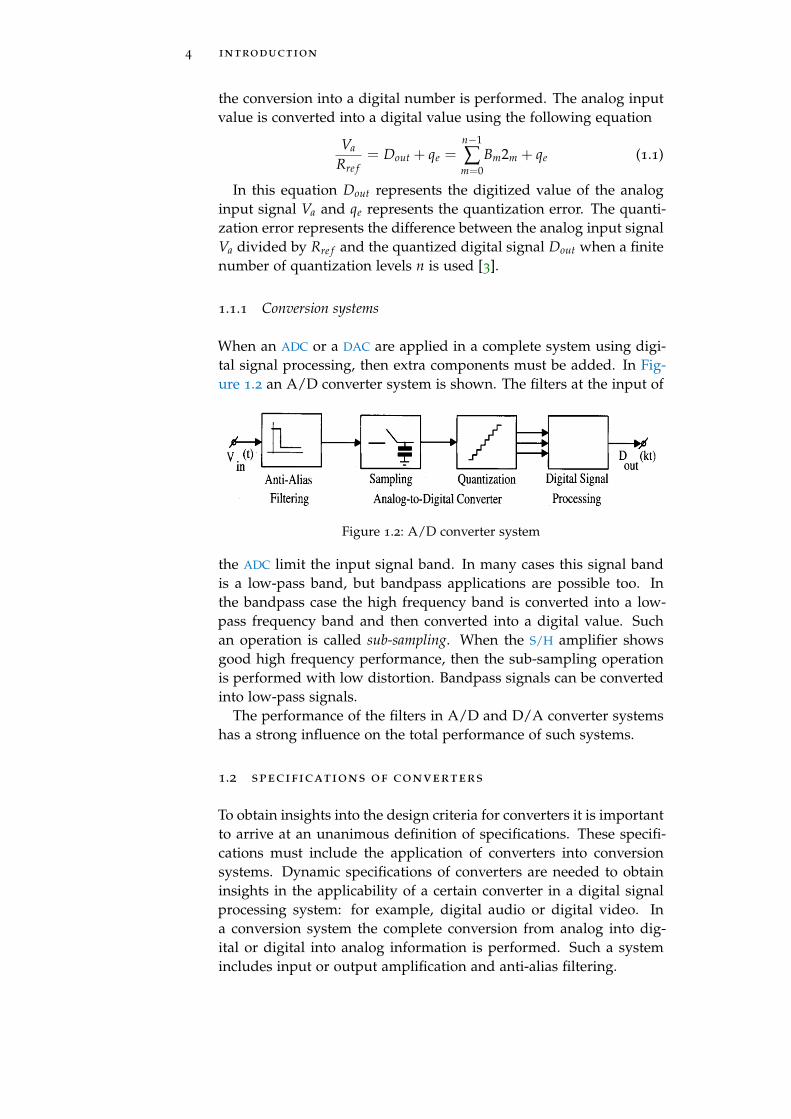
1.1.1 Conversion systems
When an ADC or a DAC are applied in a complete system using digi-tal signal processing, then extra components must be added. In Fig-ure 1.2 an A/D converter system is shown. The filters at the input of
Figure 1.2: A/D converter system
the ADC limit the input signal band. In many cases this signal bandis a low-pass band, but bandpass applications are possible too. Inthe bandpass case the high frequency band is converted into a low-pass frequency band and then converted into a digital value. Suchan operation is called sub-sampling. When the S/H amplifier showsgood high frequency performance, then the sub-sampling operationis performed with low distortion. Bandpass signals can be convertedinto low-pass signals.
The performance of the filters in A/D and D/A converter systemshas a strong influence on the total performance of such systems.
1.2 specifications of converters
To obtain insights into the design criteria for converters it is importantto arrive at an unanimous definition of specifications. These specifi-cations must include the application of converters into conversionsystems. Dynamic specifications of converters are needed to obtaininsights in the applicability of a certain converter in a digital signalprocessing system: for example, digital audio or digital video. Ina conversion system the complete conversion from analog into dig-ital or digital into analog information is performed. Such a systemincludes input or output amplification and anti-alias filtering.
1.2 specifications of converters 5
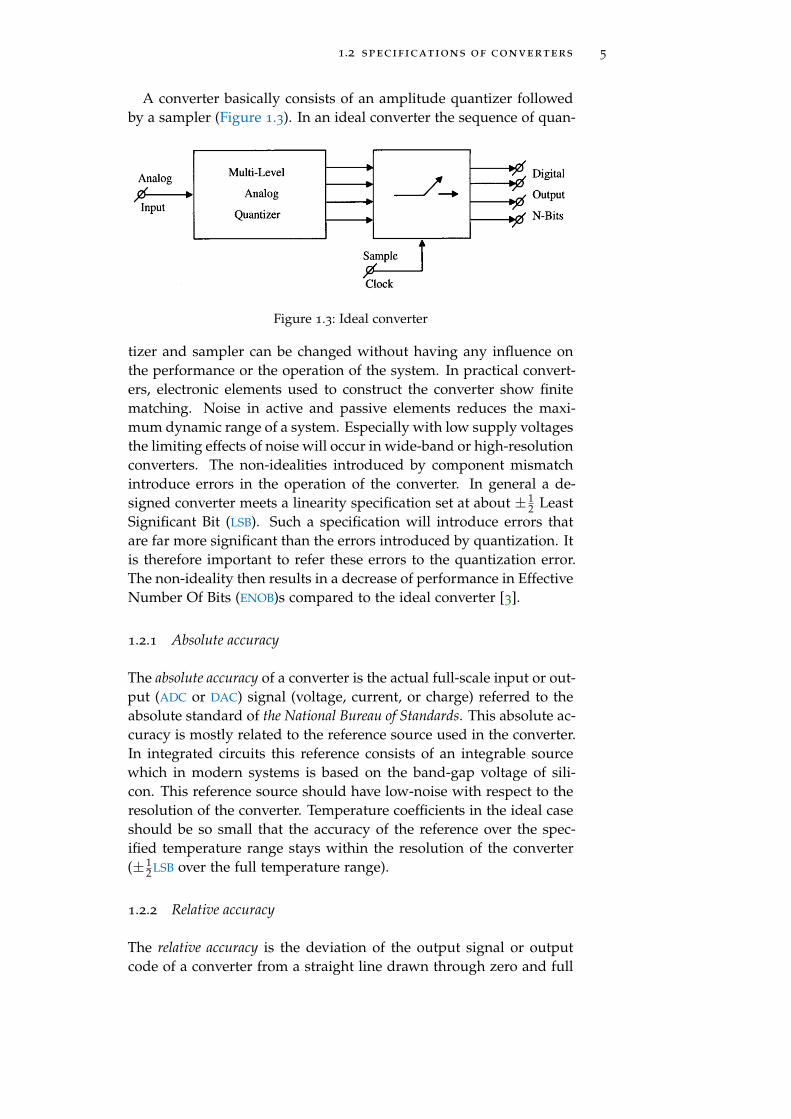
A converter basically consists of an amplitude quantizer followedby a sampler (Figure 1.3). In an ideal converter the sequence of quan-
Figure 1.3: Ideal converter
tizer and sampler can be changed without having any influence onthe performance or the operation of the system. In practical convert-ers, electronic elements used to construct the converter show finitematching. Noise in active and passive elements reduces the maxi-mum dynamic range of a system. Especially with low supply voltagesthe limiting effects of noise will occur in wide-band or high-resolutionconverters. The non-idealities introduced by component mismatchintroduce errors in the operation of the converter. In general a de-signed converter meets a linearity specification set at about ± 1
2 LeastSignificant Bit (LSB). Such a specification will introduce errors thatare far more significant than the errors introduced by quantization. Itis therefore important to refer these errors to the quantization error.The non-ideality then results in a decrease of performance in EffectiveNumber Of Bits (ENOB)s compared to the ideal converter [3].
1.2.1 Absolute accuracy
The absolute accuracy of a converter is the actual full-scale input or out-put (ADC or DAC) signal (voltage, current, or charge) referred to theabsolute standard of the National Bureau of Standards. This absolute ac-curacy is mostly related to the reference source used in the converter.In integrated circuits this reference consists of an integrable sourcewhich in modern systems is based on the band-gap voltage of sili-con. This reference source should have low-noise with respect to theresolution of the converter. Temperature coefficients in the ideal caseshould be so small that the accuracy of the reference over the spec-ified temperature range stays within the resolution of the converter(± 1
2 LSB over the full temperature range).
1.2.2 Relative accuracy
The relative accuracy is the deviation of the output signal or outputcode of a converter from a straight line drawn through zero and full
6 introduction
scale. Output signals or output codes must be corrected from a pos-sible zero offset. This relative accuracy is called Integral NonLinear-ity (INL).
The ± 12 LSB INL definition (the boundaries for which the nonlinear-
ity deviates not more than ± 12 LSB from a straight line through zero
and full scale) implies a monotonic behavior of the converter.In an ADC monotonicity means that no missing codes can occur. It
must be noted at this point that converters can be designed which areguaranteed monotonic but do not have the half LSB linearity specifi-cation. These converters are based on non-binary weighting of the bitcurrents.
In an ADC the INL definition including the quantization levels equalto
INL ≤ 12
LSB (1.2)
is valid. In case the Most Significant Bit (MSB) value is 2LSB valueslarger than the sum of all the smaller bits, then a missing code ap-pears in the converter. To guarantee monotonicity of the converter,the sum of the errors must never exceed ± 1
2 LSB value.Note that the monotonicity specification does not automatically en-
sure that a converter has an INL error less than or equal to ± 12 LSB,
while the nonlinearity specification of less than or equal to ± 12 LSB is
sufficient to prove monotonicity of a binary-weighted converter.
1.2.3 Differential nonlinearity
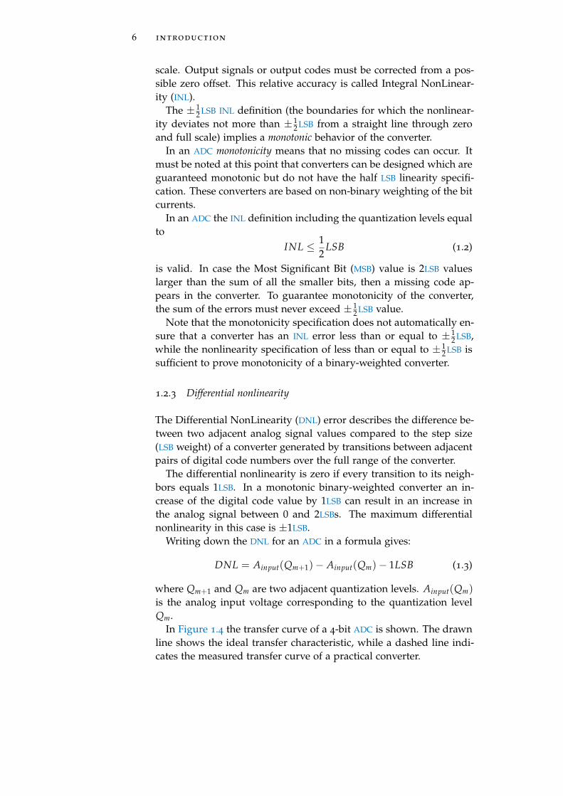
The Differential NonLinearity (DNL) error describes the difference be-tween two adjacent analog signal values compared to the step size(LSB weight) of a converter generated by transitions between adjacentpairs of digital code numbers over the full range of the converter.
The differential nonlinearity is zero if every transition to its neigh-bors equals 1LSB. In a monotonic binary-weighted converter an in-crease of the digital code value by 1LSB can result in an increase inthe analog signal between 0 and 2LSBs. The maximum differentialnonlinearity in this case is ±1LSB.
Writing down the DNL for an ADC in a formula gives:
DNL = Ainput(Qm+1)− Ainput(Qm)− 1LSB (1.3)
where Qm+1 and Qm are two adjacent quantization levels. Ainput(Qm)
is the analog input voltage corresponding to the quantization levelQm.
In Figure 1.4 the transfer curve of a 4-bit ADC is shown. The drawnline shows the ideal transfer characteristic, while a dashed line indi-cates the measured transfer curve of a practical converter.
1.2 specifications of converters 7
Figure 1.4: Transfer curve of a 4-bit ADC
1.2.4 Offset
Input amplifiers, output amplifiers, and comparators in practical cir-cuits inherently have a built-in offset voltage and offset current. Thisoffset is caused by the finite matching of components. The offset re-sults in a non-zero input or output voltage, current or digital codealthough a zero signal is applied to the converter.
1.2.5 Signal-to-Noise Ratio
The Signal-to-Noise Ratio (SNR) depends on the resolution of the con-verter and automatically includes specifications of linearity, distor-tion, sampling time uncertainty, glitches, noise, and settling time.Over half the sampling frequency, the SNR must be specified andshould ideally follow the theoretical formula
S/Nmax = 6.02n + 1.76dB (1.4)
The SNR is calculated for a sine wave input with the maximumamplitude allowed by the system. The ratio between the frequencyof the sine wave and the sampling frequency should be irrational. Incase input signals with a smaller amplitude are applied, then the SNRdecreases in accordance to the input signal decrease.

8 introduction
1.2.6 Effective Number of Bits
To get a comparison method for converters, the ENOBs is measuredunder Nyquist conditions (see Section A.2). The dynamic range of theconverter under comparison includes quantization errors, clock jittererrors, distortion errors and circuit noise. Then the ENOBs is definedas
ENOB =(SNDRmeasured)dB − 1.76
6.02dB (1.5)
with the Signal-to-Noise and Distortion Ratio (SNDR), measurementof the purity of a signal, defined [14] as
SNDR =Psignal
PquantizationError + PrandomNoise + Pdistortion(1.6)
where P is the average power of the signal, quantization error, ran-dom noise and distortion components.
Using this definition of SNDR it is very easy to compare ADCs orDACs with the same number of bits, but, due to different circuit de-signs, having different performance.
1.2.7 Figure of Merit
To compare different architectures and performances of a converterthe Figure Of Merit (FOM) has been defined. This index comparesconverters with respect to power consumption, ENOBs and maximuminput signal frequency. The FOM is defined as
FOM =Power
2 fin2ENOB (1.7)
In this equation 2 fin can be defined as the Nyquist frequency (see Sec-tion A.3), however, in case the resolution is determined by the ENOB
the input frequency can be different from the sampling frequencyand in such a case will be smaller than the Nyquist frequency. Withimproved technology and advanced converter architectures the FOM
drops about a factor every 10 years.
2A / D C O N V E RT E R S
According to the necessity of high-speed or high-accuracy ADCs, someconverter architectures are more suitables than others.
Flash converter
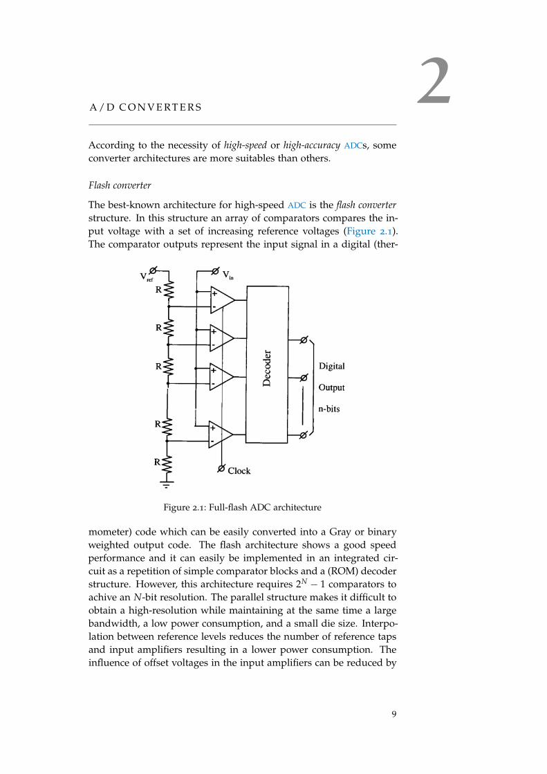
The best-known architecture for high-speed ADC is the flash converterstructure. In this structure an array of comparators compares the in-put voltage with a set of increasing reference voltages (Figure 2.1).The comparator outputs represent the input signal in a digital (ther-
Figure 2.1: Full-flash ADC architecture
mometer) code which can be easily converted into a Gray or binaryweighted output code. The flash architecture shows a good speedperformance and it can easily be implemented in an integrated cir-cuit as a repetition of simple comparator blocks and a (ROM) decoderstructure. However, this architecture requires 2N − 1 comparators toachive an N-bit resolution. The parallel structure makes it difficult toobtain a high-resolution while maintaining at the same time a largebandwidth, a low power consumption, and a small die size. Interpo-lation between reference levels reduces the number of reference tapsand input amplifiers resulting in a lower power consumption. Theinfluence of offset voltages in the input amplifiers can be reduced by
9
10 a/d converters
using averaging between active amplifier stages. At the same time,SNR is improved without using more power.
Sub ranging converter
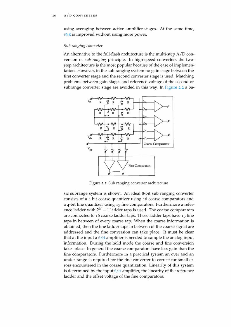
An alternative to the full-flash architecture is the multi-step A/D con-version or sub ranging principle. In high-speed converters the two-step architecture is the most popular because of the ease of implemen-tation. However, in the sub ranging system no gain stage between thefirst converter stage and the second converter stage is used. Matchingproblems between gain stages and reference voltage of the second orsubrange converter stage are avoided in this way. In Figure 2.2 a ba-
Figure 2.2: Sub ranging converter architecture
sic subrange system is shown. An ideal 8-bit sub ranging converterconsists of a 4-bit coarse quantizer using 16 coarse comparators anda 4-bit fine quantizer using 15 fine comparators. Furthermore a refer-ence ladder with 2N − 1 ladder taps is used. The coarse comparatorsare connected to 16 coarse ladder taps. These ladder taps have 15 finetaps in between of every coarse tap. When the coarse information isobtained, then the fine ladder taps in between of the coarse signal areaddressed and the fine conversion can take place. It must be clearthat at the input a S/H amplifier is needed to sample the analog inputinformation. During the hold mode the coarse and fine conversiontakes place. In general the coarse comparators have less gain than thefine comparators. Furthermore in a practical system an over and anunder range is required for the fine converter to correct for small er-rors encountered in the coarse quantization. Linearity of this systemis determined by the input S/H amplifier, the linearity of the referenceladder and the offset voltage of the fine comparators.
a/d converters 11
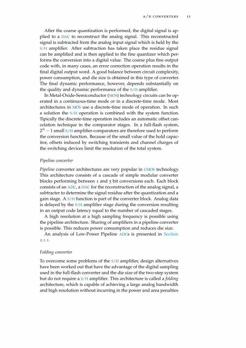
After the coarse quantization is performed, the digital signal is ap-plied to a DAC to reconstruct the analog signal. This reconstructedsignal is subtracted from the analog input signal which is held by theS/H amplifier. After subtraction has taken place the residue signalcan be amplified and is then applied to the fine quantizer which per-forms the conversion into a digital value. The coarse plus fine outputcode with, in many cases, an error correction operation results in thefinal digital output word. A good balance between circuit complexity,power consumption, and die size is obtained in this type of converter.The final dynamic performance, however, depends substantially onthe quality and dynamic performance of the S/H amplifier.
In Metal-Oxide-Semiconductor (MOS) technology circuits can be op-erated in a continuous-time mode or in a discrete-time mode. Mostarchitectures in MOS use a discrete-time mode of operation. In sucha solution the S/H operation is combined with the system function.Tipically the discrete-time operation includes an automatic offset can-celation technique in the comparator stages. In a full-flash system,2N − 1 small S/H amplifier-comparators are therefore used to performthe conversion function. Because of the small value of the hold capac-itor, offsets induced by switching transients and channel charges ofthe switching devices limit the resolution of the total system.
Pipeline converter
Pipeline converter architectures are very popular in CMOS technology.This architecture consists of a cascade of simple modular converterblocks performing between 1 and 5 bit conversions each. Each blockconsists of an ADC, a DAC for the reconstruction of the analog signal, asubtracter to determine the signal residue after the quantization and again stage. A S/H function is part of the converter block. Analog datais delayed by the S/H amplifier stage during the conversion resultingin an output code latency equal to the number of cascaded stages.
A high resolution at a high sampling frequency is possible usingthe pipeline architecture. Sharing of amplifiers in a pipeline converteris possible. This reduces power consumption and reduces die size.
An analysis of Low-Power Pipeline ADCs is presented in Section2.1.1.
Folding converter
To overcome some problems of the S/H amplifier, design alternativeshave been worked out that have the advantage of the digital samplingused in the full-flash converter and the die size of the two-step systembut do not require a S/H amplifier. This architecture is called a foldingarchitecture, which is capable of achieving a large analog bandwidthand high resolution without incurring in the power and area penalties

12 a/d converters
associated with the flash architectures (details can be found in [15,16]).
High-resolution monolithic ADCs are subject to growing interestdue to the rapidly expanding market for digital signal processing sys-tems. Monolithic converters with such a high linearity are difficult todesign and require special circuit configurations. When a low conver-sion speed is needed, integrating types of converters can be used. Inintegrating types of high-resolution ADCs basically the analog inputsignal is converted into a time which is proportional to the input sig-nal. Time is measured using a counter with an accurate clock. Thesesystems are relatively slow because of the counting operation in thetime-to-number conversion cycle. A speed improvement is obtainedby using a coarse and fine conversion cycle in the time-to-numbercounting operation. A well-known ADC based on this system is thedual slope converter.
Dual slope converter
This system consists of an input switch, an integrator with a compara-tor, a clock generator with control logic, and a counter (Figure 2.3a). The operation of the system is as follows. Starting from a reseted
(a) Dual slope ADC system (b) Dual slope ADC timing
Figure 2.3: Dual slope ADC architecture
integrator, the input signal Vin is integrated during a time t1 whichcorresponds to a full count of the counter. Then the input is switchedto the reference voltage VR having the opposite sign compared to theinput signal. The integrator is now discharged. During the dischargetime pulses are counted. Counting stops when the comparator de-tects zero. As a result, the counts in the counter represent the digitalvalue of the input signal. The timing of the operation is shown inFigure 2.3b. A simple calculation shows
Vin =t2
t1VR (2.1)
2.1 low-power adc architectures 13
Here t2 is the time during which the integrator is discharged fromthe integrated input signal to zero. As it is shown in Equation 2.1the clock is not critical; only the ratio between the charge and dis-charge times is important. A disadvantage of this system is the lowconversion speed if a high resolution is required.
Successive approximation converter
In fast and highly accurate ADCs, the successive approximation methodis commonly used. Accuracy and linearity in this system are deter-mined by the DAC, while the conversion speed depends on the com-parator response time and the settling time of the DAC. In a successiveapproximation system the analog input signal is approximated by thestep-by-step built-up analog output voltage of the DAC, starting withthe most significant bit. To obtain the high accuracy for the DAC
needed to construct a 14- to 16-bit ADC, Dynamic Element Matching isused.
Due to the construction of the bit switches, which in the high-accuracy part consist of a diode-transistor configuration, the outputvoltage swing at the D/A current output must be small. This voltageswing, called output voltage compliance, reduces the bit switchingaccuracy of the DAC. To avoid problems in this system, a specialcomparator operation is needed. In general-purpose ADCs, a generalnonlinear comparator circuit with high gain around the zero-crossinglevel is used.
SAR converters are discussed more in details in Section 2.2.
Cyclic converter
The ease with which a hold operation can be constructed allows theADC implementation using a cyclic converter algorithm. In the cyclicconverter the number of components is drastically reduced and con-sists of two S/H amplifier circuits with an accurate times two amplifierstage and a subtracter circuit. Per conversion step the remaining sig-nal is compared with a reference signal. If the remainder is largerthan the reference signal, a subtraction of the reference signal fromthe remainder is performed. The error signal that is then generatedis amplified by two and compared with the reference signal again.This operation is repeated until the total number of bits that can beconverted is obtained [3].
2.1 low-power adc architectures
It is possible to classify ADCs as Nyquist-rate or oversampling ADCs.Nyquist-rate ADCs are memoryless, and each analog sample is indi-
vidually converted into its digital equivalent. By contrast, each digitaloutput word of an oversampled ADC is derived from all preceding in-
14 a/d converters
put samples. This allows the digital output to have very short outputwords and, hence, it allows the use of simple internal quantizers.
2.1.1 Nyquist-rate ADCs
Table 2.1: Classification of Nyquist-rate ADCs( T = clock period, N = resolution in bits)
Table 2.1 shows a classification of Nyquist-rate ADCs by their algo-rithms. For micropower applications, the parallel and subrangingconverter architectures are usually unsuitable, and the counting con-verters may be too slow. Hence, the analysis will focus on pipelineand serial converters.
Low-Power Pipeline ADCs
The general architecture of a pipeline converter is shown in Figure 2.4. In general a pipeline converter consists of a cascade of identicalstages that are separated by a S/H amplifier. This S/H amplifier ispart of the sub-converter stage. Tipically the converter is preceededby a S/H amplifier. As it can be seen from Figure 2.4 the lower partof a converter stage consists of the already mentioned S/H amplifierfollowed by a p-bit analog-to-digital sub converter. This ADC drivesdirectly a p-bit DAC to reconstruct the quantized analog signal. Thisquantized analog signal is subtracted from the sampled analog inputsignal of the stage. After subtraction of the quantized signal fromthe analog input signal this residue is amplified by the gain stageand then applied to the following sub-converter stage. By pipeliningin the converter an optimization can be obtained between maximumsampling clock and the speed of the circuits used. In the first stagethe maximum accuracy is required. This accuracy depends on the res-olution the converter is designed for. After the first stage a reducedaccuracy can be applied without influencing the overall converter ac-

2.1 low-power adc architectures 15
Figure 2.4: Pipeline converter architecture
curacy too much. What architecture and what resolution are used perstage depends on the overall resolution that is required and what adesigner thinks he can achieve [3].
Most pipeline ADCs currently use the multiplied residue algorithm[17]. This requires the use of an internal ADC, a DAC and a residueamplifier in every stage. Although several of these functions can becombined by clever circuit design, the power dissipation of the circuitis usually too high for most micropower applications. An alternativepipeline configuration, based on the divided reference principle [18], isshown in Figure 2.5. Here, the analog input samples are held in
Figure 2.5: Low-power pipeline SC ADC
capacitors C1 to Cn until all bits are determined by the combination ofthe DACs and comparators. The only active elements in the circuit are
16 a/d converters
the comparators, and hence, the operation requires very little power[1].
Serial ADCs
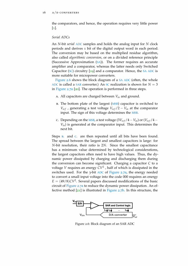
An N-bit serial ADC samples and holds the analog input for N clockperiods and derives 1 bit of the digital output word in each period.The conversion may be based on the multiplied residue algorithm,also called algorithmic conversion, or on a divided reference principle(Successive Approximation (SA)). The former requires an accurateamplifier and a comparator, whereas the latter needs only SwitchedCapacitor (SC) circuitry [19] and a comparator. Hence, the SA ADC ismore suitable for micropower converters.
Figure 2.6 shows the block diagram of a SA ADC (often, the wholeADC is called a SAR converter.) An SC realization is shown for N = 3in Figure 2.7a [20]. The operation is performed in three steps.
a. All capacitors are charged between Vin and ground.
b. The bottom plate of the largest (MSB) capacitor is switched toVre f , generating a test voltage Vre f /2− Vin at the comparatorinput. The sign of this voltage determines the MSB.
c. Depending on the MSB, a test voltage (3Vre f /4−Vin) or (Vre f /4−Vin) is generated at the comparator input. This determines thenext bit.
Steps b. and c. are then repeated until all bits have been found.The spread between the largest and smallest capacitors is large: forN-bit resolution, their ratio is 2N. Since the smallest capacitancehas a minimum value determined by technological considerations,the largest capacitors often need to have high values. Thus, the dy-namic power dissipated by charging and discharging them duringthe conversion can become significant. Charging a capacitor C to avoltage V requires an energy CV2 , half of which is dissipated in theswitches used. For the 3-bit ADC of Figure 2.7a, the energy neededto convert a small input voltage into the code 000 requires an energyE = (49/8)CV2. Several papers discussed modifications of the basiccircuit of Figure 2.7a to reduce the dynamic power dissipation. An ef-fective method [21] is illustrated in Figure 2.7b. In this structure, the
Figure 2.6: Block diagram of an SAR ADC

2.1 low-power adc architectures 17
(a) Circuit diagram of a SA ADC
(b) Low-power equivalent circuit
Figure 2.7: 3-bit SA ADC
conversion starts using the smallest, rather than the largest, capaci-tors, and additional capacitors are gradually switched into the circuit.As a result, the total power dissipation is significantly reduced; forthe generation of the code 000, the energy required is only (7/8)CV2.The average energy is reduced by about 75% compared with that inthe original structure. A design issue arising for the structure of Fig-ure 2.7b is that the required accuracy of the smallest capacitors C isincreased, since now they directly affect the MSBs.
2.1.2 Oversampled ADCs
Sigma-delta ADCs
In Figure 2.8 a general form of a sigma-delta (Σ∆) ADC system isshown. The system uses a multi-bit quantizer (ADC) and a multi-bitDAC to reconstruct the analog signal. When multi-bit DACs are usedto reconstruct the analog signal, then the linearity of such a converteris important. In case of high-resolution converters an accuracy prob-lem in the D/A system is encountered. To overcome this accuracyproblem a 1-bit system is used. In a 1-bit DAC the linearity is deter-mined by the accuracy of switching between the reference signals. Ifa high switching accuracy can be guaranteed, then a very linear sys-tem is obtained. From the input signal the output signal of the 1-bitDAC is subtracted. The difference of these two signals is filtered by
18 a/d converters
Figure 2.8: Sigma-delta ADC architecture
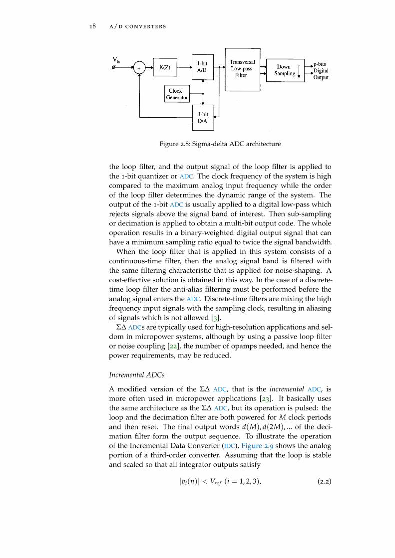
the loop filter, and the output signal of the loop filter is applied tothe 1-bit quantizer or ADC. The clock frequency of the system is highcompared to the maximum analog input frequency while the orderof the loop filter determines the dynamic range of the system. Theoutput of the 1-bit ADC is usually applied to a digital low-pass whichrejects signals above the signal band of interest. Then sub-samplingor decimation is applied to obtain a multi-bit output code. The wholeoperation results in a binary-weighted digital output signal that canhave a minimum sampling ratio equal to twice the signal bandwidth.
When the loop filter that is applied in this system consists of acontinuous-time filter, then the analog signal band is filtered withthe same filtering characteristic that is applied for noise-shaping. Acost-effective solution is obtained in this way. In the case of a discrete-time loop filter the anti-alias filtering must be performed before theanalog signal enters the ADC. Discrete-time filters are mixing the highfrequency input signals with the sampling clock, resulting in aliasingof signals which is not allowed [3].
Σ∆ ADCs are typically used for high-resolution applications and sel-dom in micropower systems, although by using a passive loop filteror noise coupling [22], the number of opamps needed, and hence thepower requirements, may be reduced.
Incremental ADCs
A modified version of the Σ∆ ADC, that is the incremental ADC, ismore often used in micropower applications [23]. It basically usesthe same architecture as the Σ∆ ADC, but its operation is pulsed: theloop and the decimation filter are both powered for M clock periodsand then reset. The final output words d(M), d(2M), ... of the deci-mation filter form the output sequence. To illustrate the operationof the Incremental Data Converter (IDC), Figure 2.9 shows the analogportion of a third-order converter. Assuming that the loop is stableand scaled so that all integrator outputs satisfy
|vi(n)| < Vre f (i = 1, 2, 3), (2.2)

2.2 successive approximation register adcs 19
Figure 2.9: Incremental ADC architecture
analysis shows that∣∣∣∣∣u− 6M(M− 1)(M− 2)
M−1
∑m=0
m−1
∑L=0
L−1
∑k=0
dout [k]Vre f
∣∣∣∣∣ ≤ 6Vre f
bc1c2M(M− 1)(M− 2)(2.3)
Hence, choosing the decimation filter as a scaled triple accumulatorlike that its output is
D =6
M(M− 1)(M− 2)
M−1
∑m=0
m−1
∑L=0
L−1
∑k=0
dout [k]Vre f (2.4)
the conversion error satisfies
|ε| = |u− D| ≤ 6Vre f
bc1c2M(M− 1)(M− 2)(2.5)
Even for high-resolution converters, M needs to be only of the orderof a few hundred clock periods. Hence, the IDC may spend a consider-able time in the sleep mode between conversions, reducing its powerdissipation. Alternatively, a single IDC may be multiplexed betweenmany sensors or channels.
Besides, the power dissipation of the IDC may further be reduced bycascading it with a Nyquist-rate ADC, for example a SAR ADC [24, 25].
2.2 successive approximation register adcs
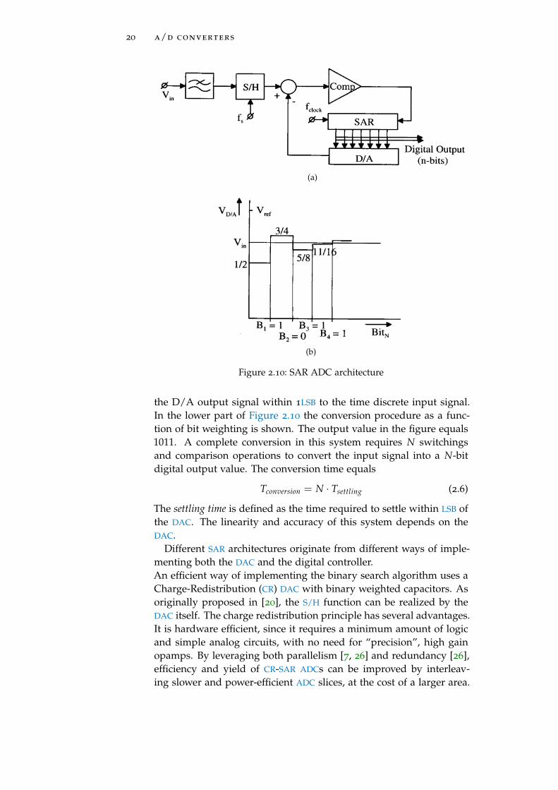
The architecture of a SAR ADC is shown in Figure 2.10. The basicconverter consists of a comparator stage (Comp), the successive ap-proximation register (SAR) and the DAC. A S/H and an anti-alias filterare added to limit the maximum analog input frequency and to con-vert the continuous time input signal into a discrete time signal. Atthe beginning of the conversion the MSB is switched on and the in-put signal is compared to the output signal of the DAC. When theinput signal is larger than the output signal of the DAC, then the MSB
remains on, the next bit is switched on and a comparison will be per-formed. A bit-by-bit operation is performed in this system to bring
20 a/d converters
(a)
(b)
Figure 2.10: SAR ADC architecture
the D/A output signal within 1LSB to the time discrete input signal.In the lower part of Figure 2.10 the conversion procedure as a func-tion of bit weighting is shown. The output value in the figure equals1011. A complete conversion in this system requires N switchingsand comparison operations to convert the input signal into a N-bitdigital output value. The conversion time equals
Tconversion = N · Tsettling (2.6)
The settling time is defined as the time required to settle within LSB ofthe DAC. The linearity and accuracy of this system depends on theDAC.
Different SAR architectures originate from different ways of imple-menting both the DAC and the digital controller.An efficient way of implementing the binary search algorithm uses aCharge-Redistribution (CR) DAC with binary weighted capacitors. Asoriginally proposed in [20], the S/H function can be realized by theDAC itself. The charge redistribution principle has several advantages.It is hardware efficient, since it requires a minimum amount of logicand simple analog circuits, with no need for “precision”, high gainopamps. By leveraging both parallelism [7, 26] and redundancy [26],efficiency and yield of CR-SAR ADCs can be improved by interleav-ing slower and power-efficient ADC slices, at the cost of a larger area.

2.2 successive approximation register adcs 21
Also, more sophisticated switching techniques have allowed reachingrecord energy efficiencies [27], by charging and discharging the ca-pacitances of CR-SAR ADCs in multiple steps or via a split capacitorbank [26, 28, 29].
A CR ADC can, however, require generating clock signals at a higherfrequency than the sample rate to drive the comparator, or sizing thecomparator for the worst case comparison time. Moreover, power-hungry active buffers may be needed for input and reference voltagesto settle within the required time and accuracy, while driving highcapacitive loads [30]. To solve the first issue, asynchronous processingcan be successfully adopted [7, 29]. To alleviate the second issue, theinput capacitance of the whole converter can be decoupled from theDAC capacitor array [27]. A DAC composed of unit capacitors (infully differential topologies) for bits of resolution is, however, stillnecessary, with possibly additional hardware to support multi-stepredistribution. A detailed analysis of the power consumption and thelinearity of capacitive-array DACs employed in SAR ADCs can be foundin [31]. At moderate resolutions, capacitor matching and insensitivityto (nonlinear) parasitics [27] provide the lower bound for the unitcapacitor size, which is certainly the ultimate limitation to furtherarea and power reductions in charge redistribution ADCs.
The need for more efficient and compact DAC implementations hasmotivated the use of series capacitive ladder networks [7], to makethe input capacitance independent of the ADC resolution, or non-binary successive approximation DACs [30], to relax the settling re-quirements on DAC and buffers at the cost of additional conversionsteps and digital processing. However, a series ladder structure canstill be vulnerable to the parasitic capacitance, especially when thecapacitor is implemented as a low-cost Metal-Oxide-Metal (MOM) ca-pacitor available in a standard digital CMOS process. Furthermore, ifthe size limit of this ladder is pushed down, expensive digital post-processing and calibration becomes unavoidable to compensate forrandom errors [7]. As an alternative approach, asynchronous Charge-Sharing (CS) SAR ADCs [8, 9] with two-stage passive S/H have alsoproved to bring power savings on the fast settling circuitry that pro-vides both the input and the reference voltages in the feedback DAC.[11]
2.2.1 Low-power SAR ADCs
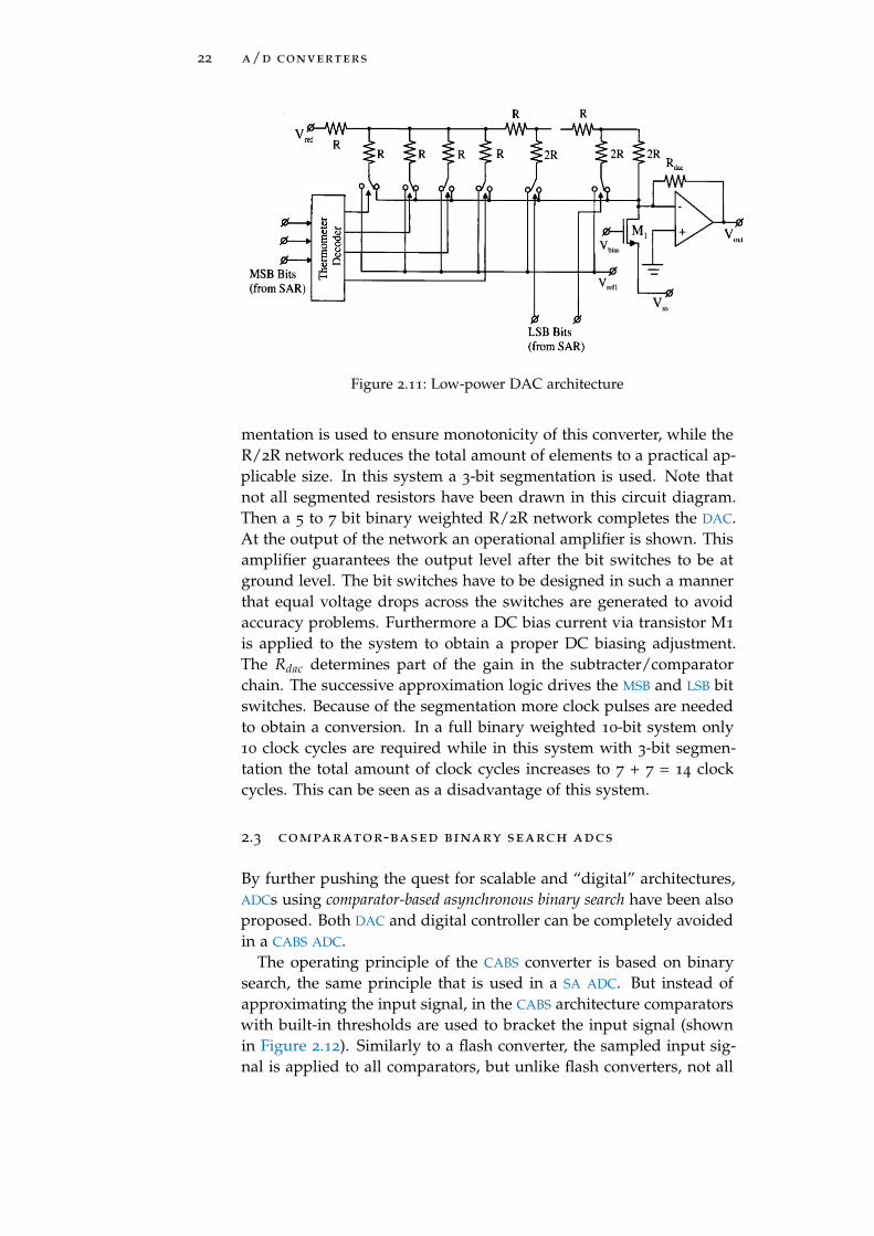
An example of a micropower successive approximation ADC is de-scribed in [32]. The important part of this design is the DAC and thecurrent subtracter circuit. The architecture is identical to the previoussystem. In Figure 2.11 the DAC architecture is shown. In the DAC seg-mentation in combination with an R/2R resistor network is shown.The segmented section is driven by the segment decoder. This seg-
22 a/d converters
Figure 2.11: Low-power DAC architecture
mentation is used to ensure monotonicity of this converter, while theR/2R network reduces the total amount of elements to a practical ap-plicable size. In this system a 3-bit segmentation is used. Note thatnot all segmented resistors have been drawn in this circuit diagram.Then a 5 to 7 bit binary weighted R/2R network completes the DAC.At the output of the network an operational amplifier is shown. Thisamplifier guarantees the output level after the bit switches to be atground level. The bit switches have to be designed in such a mannerthat equal voltage drops across the switches are generated to avoidaccuracy problems. Furthermore a DC bias current via transistor M1
is applied to the system to obtain a proper DC biasing adjustment.The Rdac determines part of the gain in the subtracter/comparatorchain. The successive approximation logic drives the MSB and LSB bitswitches. Because of the segmentation more clock pulses are neededto obtain a conversion. In a full binary weighted 10-bit system only10 clock cycles are required while in this system with 3-bit segmen-tation the total amount of clock cycles increases to 7 + 7 = 14 clockcycles. This can be seen as a disadvantage of this system.
2.3 comparator-based binary search adcs
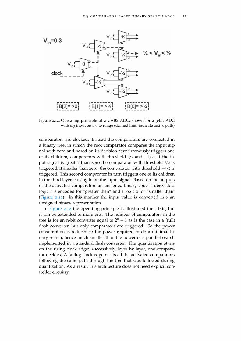
By further pushing the quest for scalable and “digital” architectures,ADCs using comparator-based asynchronous binary search have been alsoproposed. Both DAC and digital controller can be completely avoidedin a CABS ADC.
The operating principle of the CABS converter is based on binarysearch, the same principle that is used in a SA ADC. But instead ofapproximating the input signal, in the CABS architecture comparatorswith built-in thresholds are used to bracket the input signal (shownin Figure 2.12). Similarly to a flash converter, the sampled input sig-nal is applied to all comparators, but unlike flash converters, not all
2.3 comparator-based binary search adcs 23
Figure 2.12: Operating principle of a CABS ADC, shown for a 3-bit ADCwith 0.3 input on a 0 to range (dashed lines indicate active path)
comparators are clocked. Instead the comparators are connected ina binary tree, in which the root comparator compares the input sig-nal with zero and based on its decision asynchronously triggers oneof its children, comparators with threshold 1/2 and −1/2. If the in-put signal is greater than zero the comparator with threshold 1/2 istriggered, if smaller than zero, the comparator with threshold −1/2 istriggered. This second comparator in turn triggers one of its childrenin the third layer, closing in on the input signal. Based on the outputsof the activated comparators an unsigned binary code is derived: alogic 1 is encoded for “greater than” and a logic 0 for “smaller than”(Figure 2.12). In this manner the input value is converted into anunsigned binary representation.
In Figure 2.12 the operating principle is illustrated for 3 bits, butit can be extended to more bits. The number of comparators in thetree is for an n-bit converter equal to 2n − 1 as is the case in a (full)flash converter, but only comparators are triggered. So the powerconsumption is reduced to the power required to do a minimal bi-nary search, hence much smaller than the power of a parallel searchimplemented in a standard flash converter. The quantization startson the rising clock edge: successively, layer by layer, one compara-tor decides. A falling clock edge resets all the activated comparatorsfollowing the same path through the tree that was followed duringquantization. As a result this architecture does not need explicit con-troller circuitry.
24 a/d converters
Figure 2.13: Operating principle of a SAR-CC ADC, after sampling the in-put every bit is determined by a comparator which controls afeedback DAC (dashed lines indicate active path)
2.3.1 SAR ADCs using CC
Although the CABS architecture reduces power consumption in anADC, it does have the disadvantage of exponential complexity. Thiscan be avoided by implementing a SAR ADC in which the compara-tors also implement the controller function (SAR using a Comparator-based Controller (CC)). The operating principle of this architectureis shown in Figure 2.13. Once again the sampled input signal is ap-plied to all comparators in the architecture in parallel. But insteadof a tree, a chain of comparators is implemented in which each onecontrols a feedback DAC that modifies the sampled input signal. Thealgorithm implemented on this architecture is also successive approx-imation. Normally this algorithm is implemented by a synchronousor asynchronous controller, in the presented approach the compara-tors serve as state machine of the algorithm: if a comparator is resetboth “greater than” and “smaller than” outputs are zero, if it is acti-vated one of them is logic 1 and its feedback DAC modifies the inputsignal. The output of a comparator however can not immediatelytrigger the next one in the chain, since the DAC feedback signal needsto settle. Hence, an appropriate delay block with delay τ is inserted,such that the next comparator is only triggered when the feedbacksignal of the DAC is stable. Also this architecture is edge triggered,a rising clock edge at the start of the chain starts the quantization, afalling clock edge resets the structure. [5]
Recently, a Binary Search (BS) ADC implementation has been pro-posed in [6], where a switched reference voltage network and a reference-prediction circuit are used to alleviate the calibration burden, andavoid the exponential growth in comparator count respectively. Thenumber of comparator scales linearly with the ADC resolution, at
2.4 threshold-configuring adcs 25
the expense of increased complexity in the switching network, whichnow tends to grow exponentially with n.
2.4 threshold-configuring adcs
The evolution of ADCs in the last few years has been driven by thequest for both power and technology scalable architectures. Compat-ibility with advanced digital CMOS processes determines the successof highly digital architectures, such as SAR and SD ADCs for ultra-lowpower applications as wireless sensing nodes or implanted biomedi-cal devices. High research effort has been done in the recent past tointroduce highly digital architectures in ADCs for both high speed andlow power applications. The use of digital regenerative comparatorsis a key factor in the design of these novel architectures. TC-ADC wasintroduced in [10] and [11] for medium resolutions and speed, andlow power applications. It combines the principles of operation ofSAR ADCs with the use of a regenerative comparator, a programmablearray of threshold configuring transistors, and an asynchronous con-troller, allowing to implement together the ADC and DAC functionali-ties while increasing the power scalability.
2.4.1 TC-ADC Principle of Operation
The simplified schematic diagram of a TC-ADC is shown in Figure 2.14a.The principle of operation of such architecture is as follows:
a. The Track and Hold (T/H) circuitry is responsible for samplingthe analog signal – by means of its switching devices – andthen keeping constant the input terminals of the comparator –by means of the holding capacitors – until the decision is com-pleted. This funtion is done at each clock cycle, controlled bythe track signal generated in the controller.
b. The asynchronous controller initializes the comparator thresh-old to 0.0V, and generates the Track and Compare signals neededto perform the first decision, which is triggered at the fallingedge of the Track signal, as shown in Figure 2.14b. As soonas the decision is taken and notified by the raising edge of thecomparator signal Ready, the MSB of the output word, B[5], isdetermined and the comparator is reset by the falling edge ofthe Compare signal. The threshold CompTH can then be set toits next value, e.g., either +VREF/2 (if CompIN = (INp − INn) islarger than 0) or−VREF/2 (if CompIN is smaller than 0) based onthe comparator decision. A new comparison is then triggeredand the signal sequence described above repeats until all outputbits, from the MSB to the LSB, are determined.
26 a/d converters
(a) TC-ADC schematic diagram
(b) Timing diagram of a TC-ADC conversion cycle. CompIN = (INp − INn) is theinput differential voltage at the comparator, CompTH is the comparator thresholdvoltage as set by the threshold configuring devices at each conversion step
Figure 2.14: TC-ADC architecture
2.4 threshold-configuring adcs 27
The asynchronous controller provides the Track (Hold), Compare (Re-set) signals, and latches the output bits at the end of each conver-sion. Based on each comparison’s result, the controller computes, us-ing low complexity combinational logic, the necessary configurationwords to adequately shift the threshold for the next cycle. To programcomparator’s thresholds, two binary-scaled arrays of switchable ca-pacitors connected at the outputs of the latch are exploited. The dig-ital words TCA[4 : 0] and TCB[4 : 0], shown in Figure 2.14a, controlthe amount of imbalance 4C
C in the load of one of the two comparatoroutputs, which in turn generates a shift in the comparator trip point.Each switched capacitor in the arrays is implemented using PMOStransistors with short-circuited source and drain terminals, behavingas MOS varactors. [13]
2.4.2 Architectural Details
By restricting the focus to medium resolution and speed applications,it is possible to operate conversions with a minimal number of com-ponents.
A dedicated feedback DAC to generate the error signal between thesampled input and the ADC output is avoided, since the compara-tor itself implements both the A/D and D/A functionalities. In fact,since moderate resolutions are the target, the CR-DAC of a traditionalSAR ADC is conveniently replaced by a TC-ADC. The TC-ADC will alsoconsist of binary-scaled arrays of capacitors, thus presenting the samelinearity and matching requirements as the CR-DAC, for a given res-olution. However, while in CR-DACs capacitors need to be highlylinear, since they provide the gain between charge and voltage, in aTC-ADC capacitors are switched on or off in a mostly “digital” fashionto trim the trip points. These capacitors can then be implementedusing small transistors out of a standard digital technology. More-over, since no capacitors are used for the MSB decision, (2n − 2) unitdevices are required to realize an n-bit TC-ADC, which is one half ofthe total number of units (2n+1) in fully differential CR converters.
Although the comparator threshold generation mechanism can beaffected by supply voltage and temperature variations, it still bringsarea advantages and enough linearity for the target resolution [11].Moreover, “reference” voltages (except, of course, for supply volt-ages) do not need to be externally generated and buffered by possiblypower-hungry circuits. At the same time, the asynchronous operationbased on a self-timed comparator [7, 33] avoids high-speed clock gen-eration and buffering, as well as comparator design for the worst caseconversion time.
Since the target is compact solutions at moderate speeds, the se-rial conversion process is performed out of only one comparator.All thresholds are, therefore, generated out of the same comparator,

28 a/d converters
which needs to be steered by a controller during its n conversioncycles. For this reason, a TC-ADC may be slower and less power ef-ficient than a BS-ADC without controller. However, its area and com-plexity advantage can be substantial since the controller area, whichscales approximately linearly with n, is generally negligible with re-spect to other components. On the other hand, comparator area inBS-ADC with built-in thresholds shows exponential complexity, andhas been reduced to linear only with sophisticated reference switch-ing schemes [6]. Finally, an offset compensated TC-ADC at moderateresolutions can basically operate without calibration, while 2n− 1 trippoints need to be calibrated in a CABS-ADC with built-in thresholds.
2.4.3 Circuit Implementation
Here are presented analysis and design details for all the buildingblocks of a 6-bit TC-ADC.
Track-and-Hold
The T/H simply consists of two NMOS switches (with no bootstrapcircuits) that sample the input signal onto low-cost MOM capacitors.These are the only passive components in the ADC. The Track signalis generated from an external clock through a digital buffer.
Threshold-Configurable Comparator
The fully dynamic threshold-configurable comparator at the heart ofthe TC-ADC originates from a modified PMOS version of the StrongArmarchitecture [34], which has been also used in high-speed low-powerflash ADCs [35, 36].
The working principle it is based on is fully described in Chapter 3.
Digital Controller
The controller generates the Track (Hold), Compare (Reset) signals, andlatches the output bits at the end of each conversion (Figure 2.14b).Asynchronous operation enables higher sampling rates for the samepower consumption, since there is no need to generate a clock atapproximately n times the sampling frequency fs for an n-bit ADC.Moreover, a new conversion step can start as soon as the previous oneis completed in a domino-fashion, so that the sampling time needsnot be sized for the worst-case comparator’s decision time.
A conceptual, simplified block diagram of the controller is repre-sented in Figure 2.15 . The timing signals of the ADC are all derivedfrom a single ended 50% duty cycle clock input. At the beginning ofeach conversion, the clock drives the output register to latch the re-sult of previous conversion, and a pulse generator to provide the Tracksignal. Another pulse generator triggered by the end of the tracking
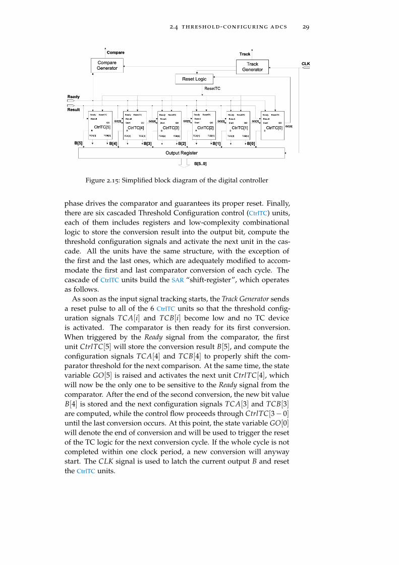
2.4 threshold-configuring adcs 29
Figure 2.15: Simplified block diagram of the digital controller
phase drives the comparator and guarantees its proper reset. Finally,there are six cascaded Threshold Configuration control (CtrlTC) units,each of them includes registers and low-complexity combinationallogic to store the conversion result into the output bit, compute thethreshold configuration signals and activate the next unit in the cas-cade. All the units have the same structure, with the exception ofthe first and the last ones, which are adequately modified to accom-modate the first and last comparator conversion of each cycle. Thecascade of CtrlTC units build the SAR “shift-register”, which operatesas follows.
As soon as the input signal tracking starts, the Track Generator sendsa reset pulse to all of the 6 CtrlTC units so that the threshold config-uration signals TCA[i] and TCB[i] become low and no TC deviceis activated. The comparator is then ready for its first conversion.When triggered by the Ready signal from the comparator, the firstunit CtrlTC[5] will store the conversion result B[5], and compute theconfiguration signals TCA[4] and TCB[4] to properly shift the com-parator threshold for the next comparison. At the same time, the statevariable GO[5] is raised and activates the next unit CtrlTC[4], whichwill now be the only one to be sensitive to the Ready signal from thecomparator. After the end of the second conversion, the new bit valueB[4] is stored and the next configuration signals TCA[3] and TCB[3]are computed, while the control flow proceeds through CtrlTC[3− 0]until the last conversion occurs. At this point, the state variable GO[0]will denote the end of conversion and will be used to trigger the resetof the TC logic for the next conversion cycle. If the whole cycle is notcompleted within one clock period, a new conversion will anywaystart. The CLK signal is used to latch the current output B and resetthe CtrlTC units.
30 a/d converters
In each CtrlTC unit, the configuration signals TCA[i] and TCB[i] aregenerated from the state variables GO and the outputs B using lowcomplexity combinational logic as follows:
TCA [i] = (B [5] + GO [i + 1]) · (B [i] · GO [i])
TCB [i] = (B [5] + GO [i + 1]) · (B [i] · GO [i]) (2.7)
After the first comparison cycle, when all the configuration arrays aredeactivated, the MSB B[5] determines which one of the two CTCA−Barrays will be configured during the subsequent conversion cycles.For instance, when B[5] is 0 and GO[i + 1] rises to 1, B[i] and GO[i]are still 0 and the TCA[i] signal becomes high, thus activating the ithunit of the CTCA array. As soon as the conversion step is completed,the signal GO[i] is set and TCA[i] will then evaluate its final logiclevel based on B[i], i.e., the current comparison result. [11]
Part II
A N U LT R A - L O W P O W E R C O M PA R AT O R
The main key in the TC-ADC operation is the understand-ing on how the digital comparator is influenced by thedigitally configurable capacitor arrays. Regenerative com-parators rely on the principle of operation of the wellknown latch–type voltage sense amplifiers used in dig-ital circuits to read the contents of different memories[37]. Latch-type comparators are well suited for theseapplications as they achieve fast decisions due to strongpositive feedback, but they are subject to static and dy-namic random offset voltages as effect of the device mis-match [38, 39]. Moreover, regenerative comparators arebased on the same principle of operation as novel FastFeedThrough Logic (FTL) logic families for digital GalliumArsenide (GaAs) [40] and CMOS [41, 42] circuits. The ba-sic operation and design methodology are described inChapter 3, while Chapter 4 presents the relationship be-tween power consumption and full scale of the Threshold-Configuring (TC)-Comparator, compared with the radiatedpower vs distance characteristic of a Radio-Frequency IDen-tification (RFID) reader.


3T H R E S H O L D - C O N F I G U R A B L E C O M PA R AT O R
As shown in Figure 3.1a1, the core comparator topology consists ofan input differential pair (M1 and M2) feeding a current into a regen-erative back-to-back inverter pair (M3 through M6).
(a) Schematic diagram
(b) Waverforms at Compare, O1 and O2 nodes
Figure 3.1: Simplified Threshold Configuring regenerative Comparator
1 This Simplified version is derived from the TC-Comparator schematic originally pre-sented in [11].
33

34 threshold-configurable comparator
3.1 basic operation
The Compare signal sets the operating phases. When Compare is low,switches NMOS S1 and S2 reset the comparator, pushing nodes O1
and O2 down to ground, so that identical initial charge conditions areput in both output nodes. In this phase, the comparator is inactiveand cleared from the previous state. No current is drawn in the circuitas Mclk is off.
When Compare goes high, the comparator is activated: the Eval-uation phase starts and Mclk is switched on, while S1 and S2 areswitched off. In this way the input differential voltage is sensed anda decision is taken by the regenerative back-to-back inverter pair.
The Evaluation phase can be approximately divided into three sub-phases.
a. At first, M1 and M2 operate in saturation regime, nodes X1 andX2 are charged almost linearly while the cross-coupled invertersare off. In this sub-phase any voltage difference between INAand INB generates an imbalance between the drain currents I1
and I2 of M1 and M2 so that the charge rate of nodes X1−2 isnot the same.
b. When the voltages of nodes X1−2 raise approximately to∣∣VTp3
∣∣(VTp is the threshold voltage of the PMOS transistors), a secondsub-phase begins, in which M3−4 start conducting and producea voltage difference between nodes O1 and O2 as well. In thissub-phase the common mode voltage at nodes X1−2 keeps grow-ing approximately from
∣∣VTp3∣∣ to VDD, while nodes O1−2 charge
up to VTn5 (VTn being the threshold voltage of the NMOS tran-sistors), still with an approximately constant slope.
c. In the third sub-phase, when M1−2 exit and M5−6 enter theirsaturation regions, the circuit mostly behaves as a cross-coupledinverter pair amplifying the initial output voltage difference tologic levels.
Finally, after the decision has been taken, no current is drawn into thecircuit as either the n or the p transistor will be off in the inverters. Atypical representation of the voltage waveforms at the internal nodesis shown in Figure 3.1b.
A NAND gate generates the Ready signal indicating when O1 andO2 assume opposite logic values and the comparison is done. Thissignal is used by the asynchronous SAR controller as a trigger to re-set the comparator and continue the conversion process with anotherthreshold configuration word. To avoid slowing down the conver-sion process, O1 and O2 are buffered by properly skewed inverters,as in [7]. For very small comparator inputs, the metastable voltageof nodes OutA and OutB is designed to fall below the NAND gate
3.2 threshold generation 35
threshold, to be interpreted as a “data ready” and pass the control tothe next conversion step.
3.2 threshold generation
If the implemented circuit was perfectly differential, the output woulddepend on the sign of the differential input, thus providing a refer-ence threshold of 0. On the other side, any mismatch purposely intro-duced between the two half-circuits causes the comparator trip pointto shift, which will result in a different “built-in” threshold. Differ-ently from [35, 36], where the input pair device widths are balanced,a relative capacitance imbalance on nodes O1−2 is exploited to createthe “reference” threshold.
A load difference 4CO = CO1 − CO2 at nodes O1−2 needs to becompensated by corresponding differences in both the charging cur-rents of O1−2 and X1−2, namely4I3 (flowing through M3−4) and4I1
(flowing through M1−2). Computing how these current differencestranslate into a trip point shift 4VIN is equivalent to analyzing thedynamic offset voltage due to output load mismatch in a latched com-parator.
A few approaches have been proposed in the literature to analyzethe input referred offset of dynamic comparators. As in the balancedmethod, described in [38], 4VIN is regarded as the compensationvoltage needed at the input terminals, to cancel the mismatch effectand ensure that the comparator reaches its balanced status in spiteof any load imbalance. This principle has been used, for instance, in[36], to evaluate the offset voltage induced by random MOS thresh-old voltage mismatch, current factor mismatch, and input pair devicewidths.
In this TC-Comparator, differently from [36] and [38], it is adopteda piece-wise linearization method, similar to the noise analysis tech-nique proposed in [43], to achieve higher modeling accuracy. Thebias point variations are tracked across the main comparator oper-ation phases, and these are accounted for all the transient currentsand voltages due to capacitance charge and discharge, as also demon-strated in [39] for a simple two-inverter latch structure. In particular,it is assumed that the circuit is solicited by a constant signal voltage4VIN , and a finite number of operating phases are defined as above(Section 3.1. Basic Operation), where the circuit is linearized and an-alyzed. Transitions between phases are assumed instantaneous, andthus neglected. The evolution of the output voltage is obtained bysolving the differential equations governing the equivalent circuit ineach phase and combining results with continuity so that the startingpoint of each phase coincides with the final point of the previous one.
The input differential voltage 4VIN required to balance the cross-coupled inverters back in their metastable state during the latch re-
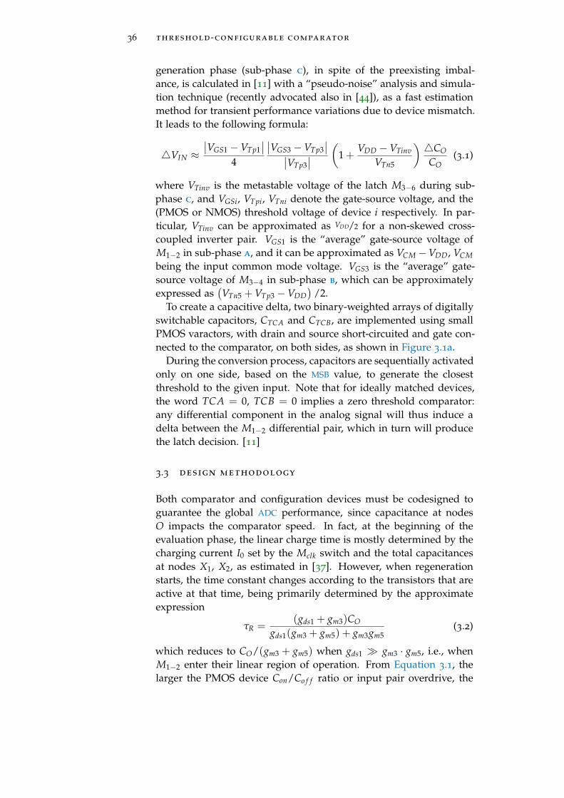
36 threshold-configurable comparator
generation phase (sub-phase c), in spite of the preexisting imbal-ance, is calculated in [11] with a “pseudo-noise” analysis and simula-tion technique (recently advocated also in [44]), as a fast estimationmethod for transient performance variations due to device mismatch.It leads to the following formula:
4VIN ≈∣∣VGS1 −VTp1
∣∣4
∣∣VGS3 −VTp3∣∣∣∣VTp3
∣∣(
1 +VDD −VTinv
VTn5
) 4CO
CO(3.1)
where VTinv is the metastable voltage of the latch M3−6 during sub-phase c, and VGSi, VTpi, VTni denote the gate-source voltage, and the(PMOS or NMOS) threshold voltage of device i respectively. In par-ticular, VTinv can be approximated as VDD/2 for a non-skewed cross-coupled inverter pair. VGS1 is the “average” gate-source voltage ofM1−2 in sub-phase a, and it can be approximated as VCM−VDD, VCMbeing the input common mode voltage. VGS3 is the “average” gate-source voltage of M3−4 in sub-phase b, which can be approximatelyexpressed as
(VTn5 + VTp3 −VDD
)/2.
To create a capacitive delta, two binary-weighted arrays of digitallyswitchable capacitors, CTCA and CTCB, are implemented using smallPMOS varactors, with drain and source short-circuited and gate con-nected to the comparator, on both sides, as shown in Figure 3.1a.
During the conversion process, capacitors are sequentially activatedonly on one side, based on the MSB value, to generate the closestthreshold to the given input. Note that for ideally matched devices,the word TCA = 0, TCB = 0 implies a zero threshold comparator:any differential component in the analog signal will thus induce adelta between the M1−2 differential pair, which in turn will producethe latch decision. [11]
3.3 design methodology
Both comparator and configuration devices must be codesigned toguarantee the global ADC performance, since capacitance at nodesO impacts the comparator speed. In fact, at the beginning of theevaluation phase, the linear charge time is mostly determined by thecharging current I0 set by the Mclk switch and the total capacitancesat nodes X1, X2, as estimated in [37]. However, when regenerationstarts, the time constant changes according to the transistors that areactive at that time, being primarily determined by the approximateexpression
τR =(gds1 + gm3)CO
gds1(gm3 + gm5) + gm3gm5(3.2)
which reduces to CO/(gm3 + gm5) when gds1 � gm3 · gm5, i.e., whenM1−2 enter their linear region of operation. From Equation 3.1, thelarger the PMOS device Con/Co f f ratio or input pair overdrive, the
3.3 design methodology 37
larger the threshold shift. However, large threshold configuration de-vices may slow down the comparator, while a larger overdrive willalso increase noise, as shown by the analysis in [43]. Since the max-imum threshold shift determines the ADC built-in VREF, CTCA−B de-vices and input pair overdrive must be sized to provide the desireddynamic range. Based on estimations of the total decision time from[37] and Equation 3.2, in [11] it is derived a time-varying, nonlin-ear behavioral model of the comparator, which also includes non-stationary noise effects and nonlinearities in the threshold generationmechanism.

4D E S I G N S P E C I F I C AT I O N R E Q U I R E M E N T S
The TC-Comparator performance optimization, object of this study,could not be properly elaborated whitout well-defined criteria to in-dentify the exact value of Vth for each digital code.
4.1 tc-comparator power consumption vs full scale
Looking into the best optimization methodology to adopt for the TC-Comparator elements sizing led to the plain necessity of being ableto search and define the threshold voltage Vth related to each digitalcode included into the comparator full-scale. Vth is used indeed as“reference value” inside the range of vid values corresponding to eachdigital code, due to the non-linear relationship between vid and digitalcodes (Figure 7.3).
The first investigation and optimization method adopted was thescanning mode (described in Section 5.1.1; script of the correspondingsheader.sp file presented in Section A.7.1). This method of analysisby parameters variation turned out to be too slow for the main aim,that is the sizing optimization, but powerful for detecting the mostprecise value of Vth for each digital code included into the full-scale.In Figure 4.1 it is described how the scanning mode can detect eachVth value with the required precision, in a performance vs vid outputplot. Due to the finite precision provided by the calculator and the in-trinsic delay time shown by the comparator before the output signalsgo to the High or Low level (Figure 5.5b), the performance vs vid tracesresult non-asymptotic. Anyway, Vth values can be limited within adefined range with sufficient precision, by applying the following it-erative algorithm:
1. Fix a digital code.
2. Set the region to a maximum (absolute) value. (Note that onlyhalf of all possible voltage values are swept. Note also that thelimit value for the first iteration should be the largest possible,that is the power supply voltage value, in this case −1.0V).
3. Sweep inside the defined region.
4. Plot the output performance vs vid.
5. Redefine the (narrower) sweeping region.
6. Go to 3.
39
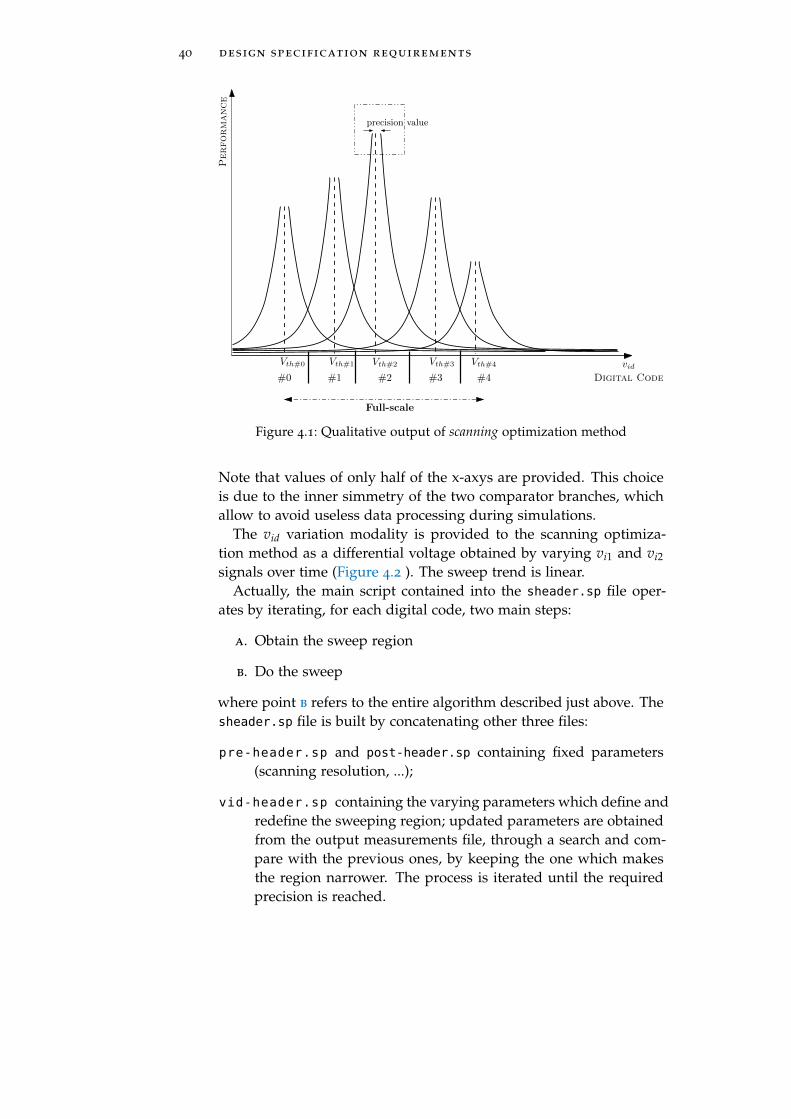
40 design specification requirements
Performance
vidDigital Code#1#0 #2 #3 #4
Vth#0 Vth#1 Vth#2 Vth#3 Vth#4
Full-scale
precision value
Figure 4.1: Qualitative output of scanning optimization method
Note that values of only half of the x-axys are provided. This choiceis due to the inner simmetry of the two comparator branches, whichallow to avoid useless data processing during simulations.
The vid variation modality is provided to the scanning optimiza-tion method as a differential voltage obtained by varying vi1 and vi2signals over time (Figure 4.2 ). The sweep trend is linear.
Actually, the main script contained into the sheader.sp file oper-ates by iterating, for each digital code, two main steps:
a. Obtain the sweep region
b. Do the sweep
where point b refers to the entire algorithm described just above. Thesheader.sp file is built by concatenating other three files:
pre-header.sp and post-header.sp containing fixed parameters(scanning resolution, ...);
vid-header.sp containing the varying parameters which define andredefine the sweeping region; updated parameters are obtainedfrom the output measurements file, through a search and com-pare with the previous ones, by keeping the one which makesthe region narrower. The process is iterated until the requiredprecision is reached.
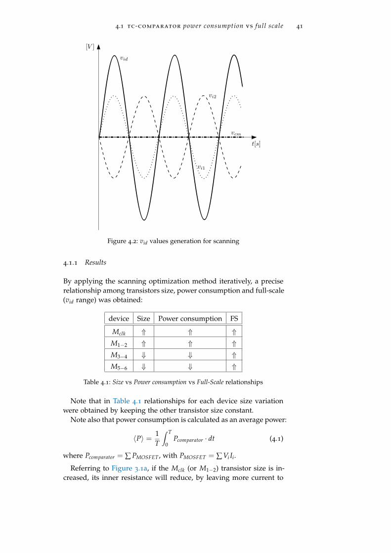
4.1 tc-comparator power consumption vs full scale 41
vcm
vi1
vid
vi2
[V ]
t[s]
Figure 4.2: vid values generation for scanning
4.1.1 Results
By applying the scanning optimization method iteratively, a preciserelationship among transistors size, power consumption and full-scale(vid range) was obtained:
device Size Power consumption FS
Mclk ⇑ ⇑ ⇑M1−2 ⇑ ⇑ ⇑M3−4 ⇓ ⇓ ⇑M5−6 ⇓ ⇓ ⇑
Table 4.1: Size vs Power consumption vs Full-Scale relationships
Note that in Table 4.1 relationships for each device size variationwere obtained by keeping the other transistor size constant.
Note also that power consumption is calculated as an average power:
〈P〉 = 1T
∫ T
0Pcomparator · dt (4.1)
where Pcomparator = ∑ PMOSFET, with PMOSFET = ∑ Vi Ii.
Referring to Figure 3.1a, if the Mclk (or M1−2) transistor size is in-creased, its inner resistance will reduce, by leaving more current to
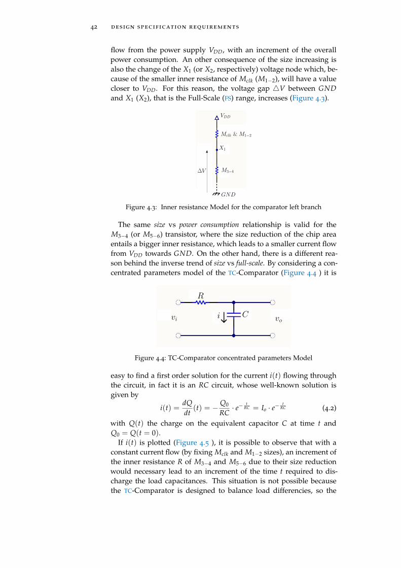
42 design specification requirements
flow from the power supply VDD, with an increment of the overallpower consumption. An other consequence of the size increasing isalso the change of the X1 (or X2, respectively) voltage node which, be-cause of the smaller inner resistance of Mclk (M1−2), will have a valuecloser to VDD. For this reason, the voltage gap 4V between GNDand X1 (X2), that is the Full-Scale (FS) range, increases (Figure 4.3).
Mclk & M1−2
X1
M3−4
VDD
GND
∆V
Figure 4.3: Inner resistance Model for the comparator left branch
The same size vs power consumption relationship is valid for theM3−4 (or M5−6) transistor, where the size reduction of the chip areaentails a bigger inner resistance, which leads to a smaller current flowfrom VDD towards GND. On the other hand, there is a different rea-son behind the inverse trend of size vs full-scale. By considering a con-centrated parameters model of the TC-Comparator (Figure 4.4 ) it is
R
Civi vo
Figure 4.4: TC-Comparator concentrated parameters Model
easy to find a first order solution for the current i(t) flowing throughthe circuit, in fact it is an RC circuit, whose well-known solution isgiven by
i(t) =dQdt
(t) = − Q0
RC· e− t
RC = Io · e−t
RC (4.2)
with Q(t) the charge on the equivalent capacitor C at time t andQ0 = Q(t = 0).
If i(t) is plotted (Figure 4.5 ), it is possible to observe that with aconstant current flow (by fixing Mclk and M1−2 sizes), an increment ofthe inner resistance R of M3−4 and M5−6 due to their size reductionwould necessary lead to an increment of the time t required to dis-charge the load capacitances. This situation is not possible becausethe TC-Comparator is designed to balance load differencies, so the

4.1 tc-comparator power consumption vs full scale 43
i(t)
t
∆t
i = cost
Light C load Heavy C load
Figure 4.5: Qualitative analysis of the current i flowing through the com-parator branches
only solution is a current increase, which once again implies a biggerFS range.

44 design specification requirements
4.2 rfid reader radiated power vs distance
The DC chip power consumption (Pcons) and the efficiency in the RFinto DC power conversion (η) are the factors that limit the operationrange in a passive tag. For better understanding this statement, theFriis Transmission Equation (4.3) is introduced. This equation givesthe power transmitted from one antenna to another, in free space:
Pr
Pt= GrGt
(λ
4πd
)2
(4.3)
Here Pt is the power fed into the transmitting antenna at its input ter-minals; Pr is the power available at the output terminal of the receiv-ing antenna; Gr and Gt are the gains of the receiving and transmittingantenna, respectively; λ is the wavelength; d is the distance betweenthe antennas (see Figure 4.6 ).
Figure 4.6: Illustration of the Friis Transmission Formula
For proper operation it is indispensable that
Pr ≥ ηPcons (4.4)
where Pcons is the upper bound of the power consumption on chipand η is the RF into DC power conversion efficiency. If condition (4.4)is not verified, there will not be enough power available to supplythe chip. Assuming that PtGt is limited by governmental regulationsin Europe to 2W Effective Radiated Power (ERP), with a frequency of868MHz, a typical value for Gr is 2.5dBi, with polarization losses of3dB; the function Pr vs d is illustrated in Figure 4.7.

4.2 rfid reader radiated power vs distance 45
Figure 4.7: Available power at the output of the receiving antenna as a func-tion of the distance
The figure shows the power that reaches the tag as a function ofthe distance, without considering obstacles and reflections. It is clearthat tags consumption severely limits the operation range of the sys-tem. For an operation range of 2 meters, it will require a factorηPcons ≤ 520µW. Hence assuming η = 20%, the upper bound ofthe power consumpion on chip with 2 meters between antennas isPcons = 2.6mW [45].


Part III
S I Z I N G A N D O P T I M I Z AT I O N
Simulations developed in this study aim at obtaining thebest chip sizes for a power optimized design of a TC-Comparator.Wonder to attain this goal, a Simulation environment set-up must be preliminarily defined (Chapter 5). Afterwards,process corner and variation parameters are set into thesimulator scripts for the selected technology process model(Chapter 6). Finally, results are obtained and analyzed indifferent linearity and mismatch conditions.


5S I M U L AT I O N E N V I R O N M E N T S E T- U P
To be able to evaluate the TC Comparator behaviour and which pa-rameters are critical for its optimization, it is foundamental to de-velop a Simulation Environment where obtaining values related tothe adopted technology, the UMC CMOS 90 nm “Standard Process1.0V CMOS 1P9M”.
5.1 hspice environment structure
HSPICE is a program that, starting from a circuit description andanalysis options, outputs the analysis it has done on that circuit.
Doing an HSPICE simulation requires some input elements, asshown in Figure 5.1 ; in particular, it must be provided that:
• the Technology File, containing the reference parameters of theUMC CMOS 90 nm “Standard Process 1.0V CMOS 1P9M” tech-nology;
• the Netlist, a set of files, typically with a .sp extension. Itsstructure is decribed in Figure 5.2 ;
• the Measurements File, where the parameters that it is necessaryto monitor are defined;
• the Corner of Process with a defined variance σ, required forMonte Carlo Analysis (see Section A.4).
Although HSPICE produces many output files, the main one is thefile with .lis extension, for example circuit.lis. This file containsall the important results from the HSPICE analysis: operating points,measurement results, error messages. Typically after simulating acircuit, it is better to check this file first in order to ensure there wereno errors in the netlist. The other files that HSPICE generates areused by GnuPlot, a portable command-line driven graphic utility thatallows to graphically plot HSPICE analysis results.
49
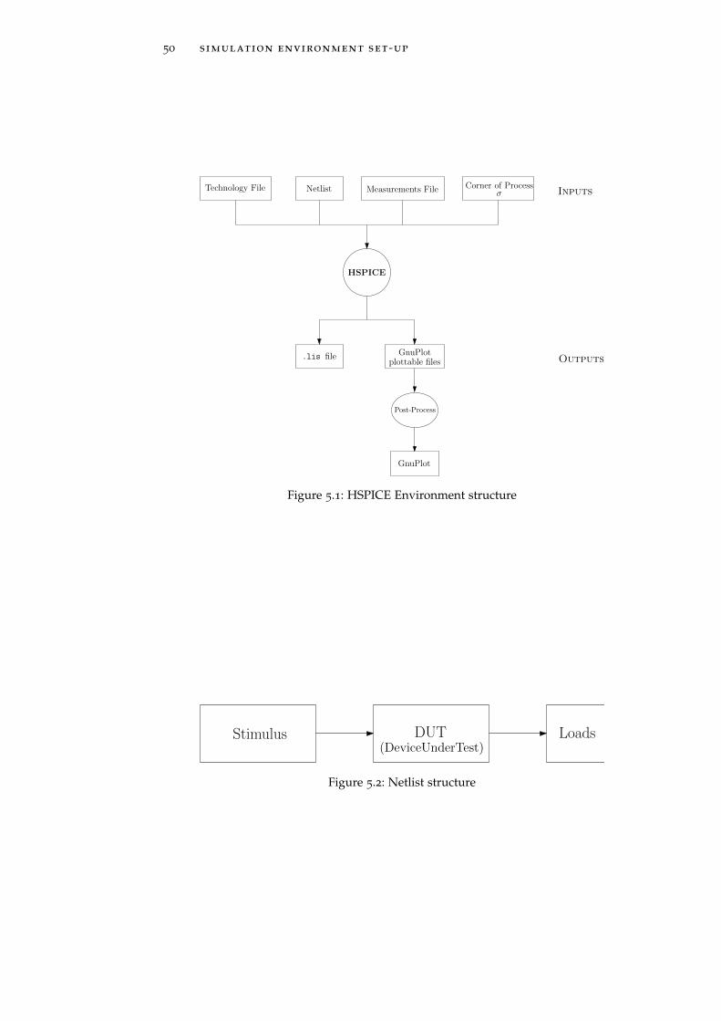
50 simulation environment set-up
HSPICE
Technology File Netlist Measurements File Corner of Processσ
.lis file GnuPlotplottable files
GnuPlot
Post-Process
Inputs
Outputs
Figure 5.1: HSPICE Environment structure
Stimulus DUT(DeviceUnderTest)
Loads
Figure 5.2: Netlist structure

5.1 hspice environment structure 51
5.1.1 Files Hierarchy
From a detailed analysis of the virtual workspace used during thesimulation workflow, it appears what follows:
bin/ It contains the main command files used to run the simulations;in particular:
go it works structurally over the tcadc command file, allowingto iterate the simulation with some parameters variations;
tcadc the properly called main file containing the preprocess-ing simulation directives (see Section A.6) . It presents thefollowing internal structure:
title ’Threshold Voltage Determination’
options
lib L90_SP10_V031_MC_CORNER.lib,where CORNER means that the Typical Corner ProcessModel is adopted
includes
• parameters
• global nets
• inputs/stimulus
• netlist
the top netlist
measurements
probe points
optimization models contains variation values in or-der to evaluate performances in terms of [AVeRage(AVG) and Root Mean Square (RMS)] power dissipation,current and voltage (see Section A.7)
sheader.sp Scanning optimization mode (Section A.7.1).It contains a number of .alter commands, whichmodify any previous HSPICE sentence. In particu-lar, these commands operate on x-axis parameterslike
• vid
• digital code
oheader.sp Bisection optimization mode (Section A.7.2)
mheader.sp Monte Carlo optimization mode (Section A.7.3)
extractor it is fundamental for data postprocessing, as it ex-tracts data from the measurements output files and gener-ates tables of data in the right format for GnuPlot graphicanalysis.
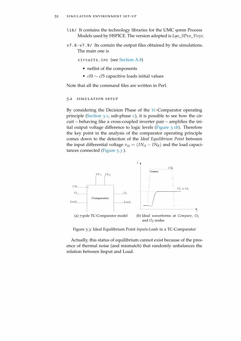
52 simulation environment set-up
lib/ It contains the technology libraries for the UMC 90nm ProcessModels used by HSPICE. The version adopted is L90_SP10_V031.
v7.6-v7.9/ Its contain the output files obtained by the simulations.The main one is
circuits.inc (see Section A.8)
• netlist of the components
• cl0 ∼ cl5 capacitive loads initial values
Note that all the command files are written in Perl.
5.2 simulation setup
By considering the Decision Phase of the TC-Comparator operatingprinciple (Section 3.1, sub-phase c), it is possible to see how the cir-cuit – behaving like a cross-coupled inverter pair – amplifies the ini-tial output voltage difference to logic levels (Figure 3.1b). Thereforethe key point in the analysis of the comparator operating principlecomes down to the detection of the Ideal Equilibrium Point betweenthe input differential voltage vid = (INA − INB) and the load capaci-tances connected (Figure 5.3 ).
O2
Load2Load1
O1
Clk
INA INB
Comparator
(a) 7-pole TC-Comparator model
O1 ≡ O2
Clk
V
t
(b) Ideal waverforms at Compare, O1and O2 nodes
Figure 5.3: Ideal Equilibrium Point Inputs-Loads in a TC-Comparator
Actually, this status of equilibrium cannot exist because of the pres-ence of thermal noise (and mismatch) that randomly unbalances therelation between Imput and Load.

5.2 simulation setup 53
INPUT
LOAD
Noise
INPUT
LOAD
Noise
(a) (b)
Figure 5.4: Imbalance between Input and Load due to thermal noise
The strategy adopted to pick out the searched threshold voltage Vth(for each digital code) can be described as follows.
Given a defined input load, for INA ≡ INB, outputs O1−2 are ob-tained. Subsequently, the minimum value of vid
Vth = min(vid) = min(INA − INB) (5.1)
necessary for changing the outputs will be revealed (Figure 5.5 ).This value can be numerically determined using an optimization
procedure implemented in HSPICE, the Bisection Methodology, whichuses a binary search method to find the value of an input variable(see Section A.5).
The Bisection Method requires the definition of a precision variable,used like decision parameter. The most suitable choice in this case isO(T) measured at time T, defined as
O(T) = O1(T)−O2(T) (5.2)
At this point, Vth is obtained by two successive simulations, whichgive:
V−th = Vth −ε
IN
V+th = Vth +
εIN (5.3)
where
V−th = vid|O1>O2
V+th = vid|O2>O1ε
IN ' ε · vid, ε� 1
By recursively repeating these simulations, it is possible to obtaina value for Vth with the required precision.
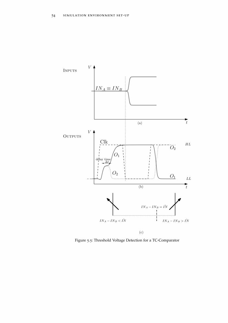
54 simulation environment set-up
Clk
O1
O2
Inputs
Outputs
INA − INB = ˜IN
INA − INB < ˜IN INA − INB > ˜IN
O1
O2
(a)
(b)
(c)
HL
LL
delay time∆t
Figure 5.5: Threshold Voltage Detection for a TC-Comparator
6S I Z I N G F O R U LT R A - L O W P O W E R A N D F SO P E R AT I O N
Defining Integrated Circuit performance without further qualificationis somewhat subjective. However for the purpose of comparison, it ispossible to quantify performance in terms of three parameters: powerdissipation, functional throughput rate and communication limits. Incomputationally intensive structures, usually one has to address thebest approach that can be pursued to partition a given system. Forexample, the question that may arise in this process is the choice as towhether one creates a very high speed single channel or to take thealternative approach of partitioning the system into parallel channelsclocked at lower frequency. However, according to design specifica-tion of an ultra-low power ADC for blood pressure applications, thesuitable technology needs to satisfy the following criteria:
• Very low propagation delay possibly less than 100ps/gate;
• Low gate dissipation in order of 100µW/gate;
• Very low dynamic switching energy, that is less than 0.1pJ;
• Very high level of integration, greater than 50000 gates;
• High process yield.
6.1 characteristics of cmos devices
The CMOS device is the key active device used in the Comparatorcircuits. Therefore a comparison of processes must consider the gain-bandwidth product ft, transconductance gm, parasitic capacitancesand resistances of the Metal-Oxide-Semiconductor Field-Effect Tran-sistor (MOSFET) to evaluate circuit performance.
6.1.1 Threshold voltage
Threshold voltage, Vth, is defined as the minimum gate electrode biasrequired to strongly invert the surface under the poly and form aconducting channel between the source and the drain regions. Vthis usually measured at a drain-source current of 250µA. Commonvalues are 2− 4V for high voltage devices with thicker gate oxides,and 1− 2V for lower voltage, logic-compatible devices with thinnergate oxides. With power MOSFETs finding increasing use in portableelectronics and wireless communications where battery power is at
55

56 sizing for ultra-low power and fs operation
a premium, the trend is toward lower values of Vth and RDS(on),withRDS(on) the on-state resistance of a power MOSFET (defined inSection 6.1.3).
6.1.2 Maximum drain-source Currents
The drain-source current is the maximum current the MOSFET hasavailable to drive the circuit. A large value implies the MOSFET isable to drive large capacitive loads, however the power dissipationdirectly increases. Sub-threshold current flows from drain to sourcewhen the gate to source voltage is below the pinch off voltage. This iswhen electrons are transported in the channel by diffusion and drift.
6.1.3 Parasitic Capacitance and on-state Resistance
The gate capacitance of a MOSFET is the major limiting factor ofcircuit speed if the interconnect lengths are short, as is the case indensely packed VLSI circuits. Cgs0 and Cgd0 are the gate-source andgate-drain zero-bias junction capacitances per micron gate width re-spectively. These are used to model the gate capacitance of MOS-FET’s.
The on-state resistance of a power MOSFET is made up of severalcomponents as shown in Figure 6.1 :
RDS(on) = Rsource + Rch + RA + RJ + RD + Rsub + Rwcml(6.1)
Rsource =Source diffusion resistance
Rch =Channel resistance
RA =Accumulation resistance
RJ ="JFET" component - resistance of the region
between the two body regions
RD =Drift region resistance
Rsub =Substrate resistance
Rwcml = Sum of bond wire resistance, metallization
and leadframe contributions
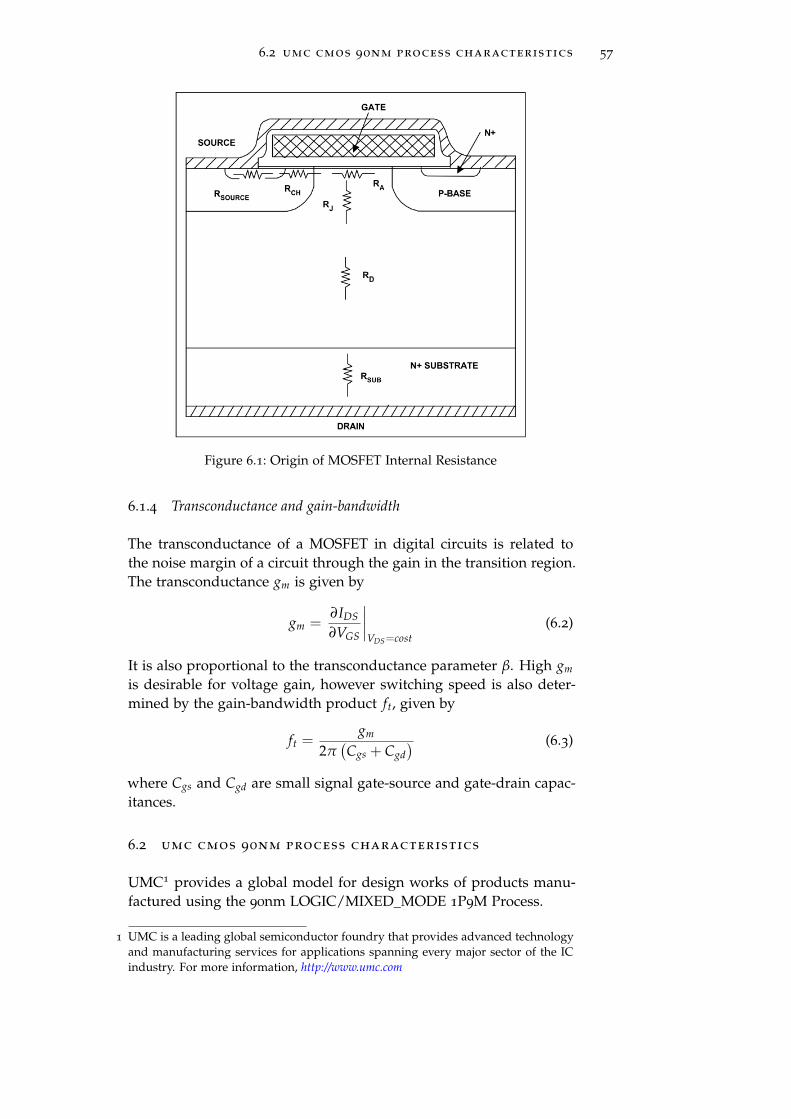
6.2 umc cmos 90nm process characteristics 57
Figure 6.1: Origin of MOSFET Internal Resistance
6.1.4 Transconductance and gain-bandwidth
The transconductance of a MOSFET in digital circuits is related tothe noise margin of a circuit through the gain in the transition region.The transconductance gm is given by
gm =∂IDS
∂VGS
∣∣∣∣VDS=cost
(6.2)
It is also proportional to the transconductance parameter β. High gm
is desirable for voltage gain, however switching speed is also deter-mined by the gain-bandwidth product ft, given by
ft =gm
2π(Cgs + Cgd
) (6.3)
where Cgs and Cgd are small signal gate-source and gate-drain capac-itances.
6.2 umc cmos 90nm process characteristics
UMC1 provides a global model for design works of products manu-factured using the 90nm LOGIC/MIXED_MODE 1P9M Process.
1 UMC is a leading global semiconductor foundry that provides advanced technologyand manufacturing services for applications spanning every major sector of the ICindustry. For more information, http://www.umc.com
58 sizing for ultra-low power and fs operation
To cope with the impact of process variations on circuit perfor-mance, worst-case models are provided along with the typical caseand they are listed below. Note that “fast” here means lower thresh-old voltage, higher leakage and driving current, and “slow” meanshigher threshold voltage, lower leakage and driving current.
tt : Typical n-ch MOSFET and Typical p-ch MOSFET
ff : Fast n-ch MOSFET and Fast p-ch MOSFET
ss : Slow n-ch MOSFET and Slow p-ch MOSFET
fnsp : Fast n-ch MOSFET and Slow p-ch MOSFET
snfp : Slow n-ch MOSFET and Fast p-ch MOSFET
The provided model is valid within the following geometry (Table 6.1),voltage (Table 6.2), and temperature (Table 6.3) ranges. Device behav-ior beyond these ranges may not be well described by the model andis not guaranteed.
1.0 V n-ch MOSFET 1.0 V p-ch MOSFET
0.08µm ≤ LDES ≤ 50µm 0.08µm ≤ LDES ≤ 50µm
0.12µm ≤WDES ≤ 100µm 0.12µm ≤WDES ≤ 100µm
(adopt multi-finger structures if WDES > 10µm) (adopt multi-finger structures if WDES > 10µm)
0.24µm ≤ SA, SB 0.24µm ≤ SA, SB
0.28µm ≤ SD(NF > 1) 0.28µm ≤ SD(NF > 1)
Note: SAREF = SBREF = 1.76µm is the reference dimension of theSTI-stress effect.
Table 6.1: Geometry range for UMC CMOS 90nm Process Model
1.0 V n-ch MOSFET 1.0 V p-ch MOSFET
0V ≤ VGS ≤ 1.0V(∗1.1) 0V ≥ VGS ≥ −1.0V(∗1.1)
0V ≤ VDS ≤ 1.0V(∗1.1) 0V ≥ VGDS ≥ −1.0V(∗1.1)
1.0V ≤ VBS ≤ 0V 1.0V ≥ VBS ≥ 0V
Table 6.2: Voltage range for UMC CMOS 90nm Process Model
1.0 V n-ch MOSFET 1.0 V p-ch MOSFET
−55°C ∼ +125°C −55°C ∼ +125°C
Table 6.3: Temperature range for UMC CMOS 90nm Process Model
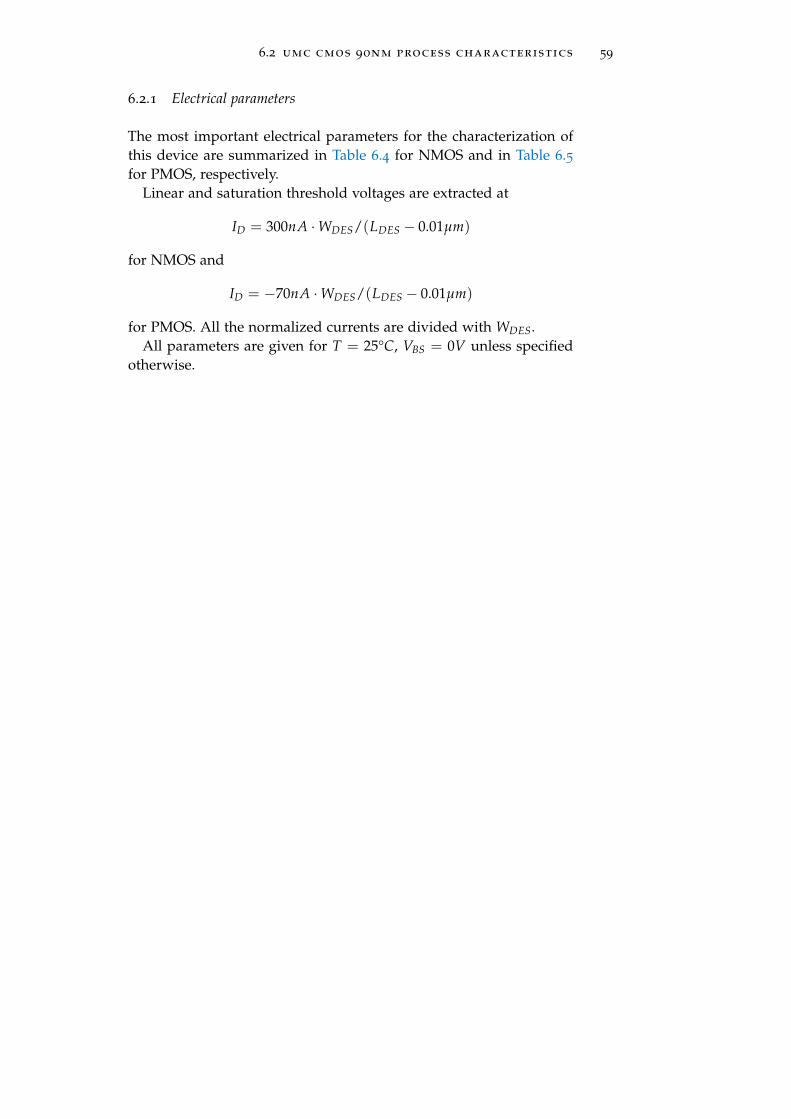
6.2 umc cmos 90nm process characteristics 59
6.2.1 Electrical parameters
The most important electrical parameters for the characterization ofthis device are summarized in Table 6.4 for NMOS and in Table 6.5for PMOS, respectively.
Linear and saturation threshold voltages are extracted at
ID = 300nA ·WDES/(LDES − 0.01µm)
for NMOS and
ID = −70nA ·WDES/(LDES − 0.01µm)
for PMOS. All the normalized currents are divided with WDES.All parameters are given for T = 25°C, VBS = 0V unless specified
otherwise.
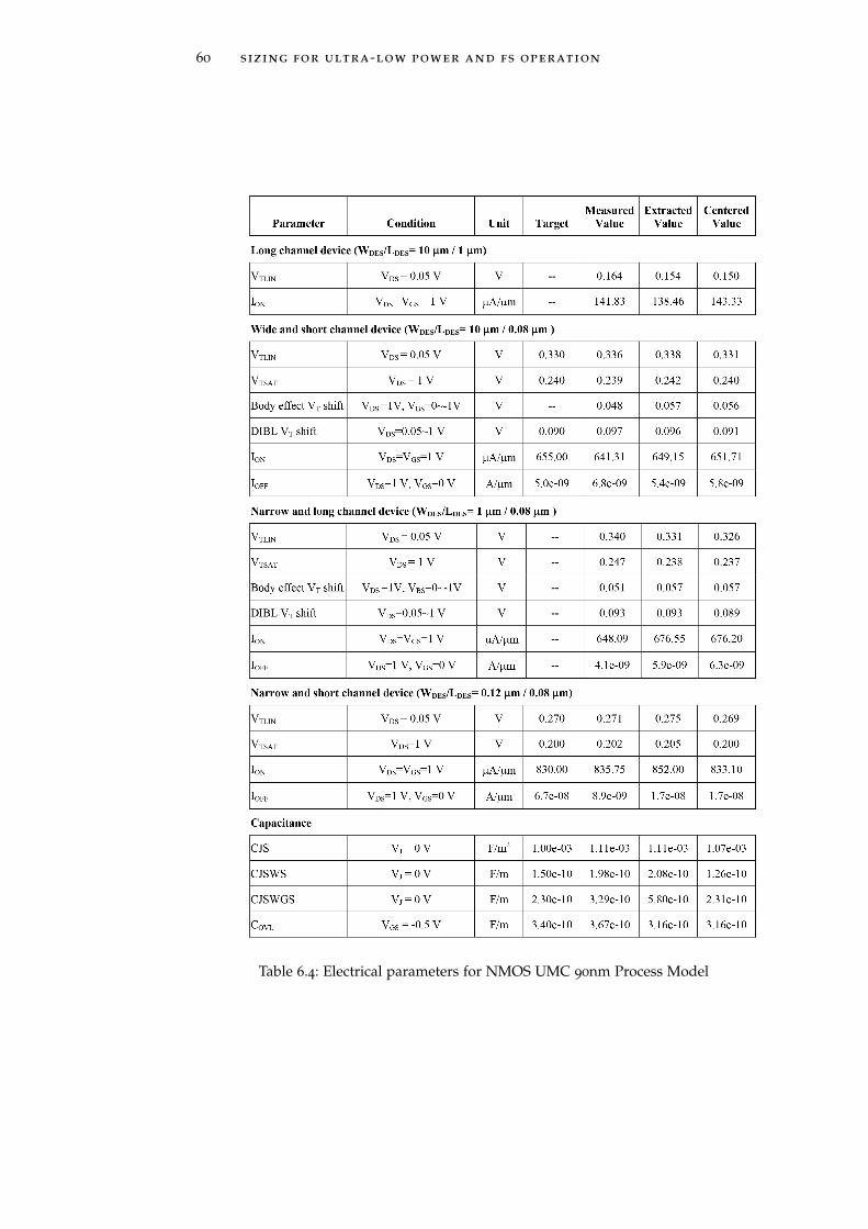
60 sizing for ultra-low power and fs operation
Table 6.4: Electrical parameters for NMOS UMC 90nm Process Model
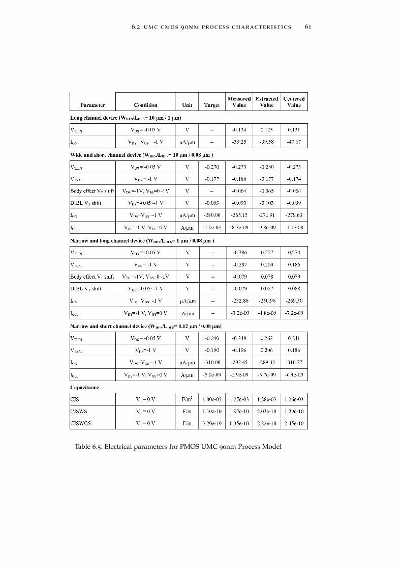
6.2 umc cmos 90nm process characteristics 61
Table 6.5: Electrical parameters for PMOS UMC 90nm Process Model
62 sizing for ultra-low power and fs operation
6.2.2 Model fitting accuracy
The model fitting accuracy of parameters ID, GM and GDS (Table 6.11)is quantified by using the following equation:
error% = 100 · |meaasurement− simulation|measurement+simulation
2
(6.4)
Different error criteria are defined for different parameters (ID, GM
and GDS) as well as for different operation region. These criteria areexplained below.
a. ID accuracy criteria
a) ID in sub-threshold region, i.e. VGS < VT;
b) ID in moderate inversion region, that is VT ≤ VGS < VT +
VX;
c) ID in strong inversion region, that is VT +VX ≤ VGS ≤ VCC;where VX = (VCC −VT)/2
b. GM and GDS accuracy criteria
a) GM and GDS in sub-threshold region, that is VGS < VT
b) GM and GDS in inversion region, that is VT ≤ VGS ≤ VCC
In-depth analysis about Worst Case model and other parameters trendscan be retrieved in [46].
Table 6.11: Requirement for model fit accuracy
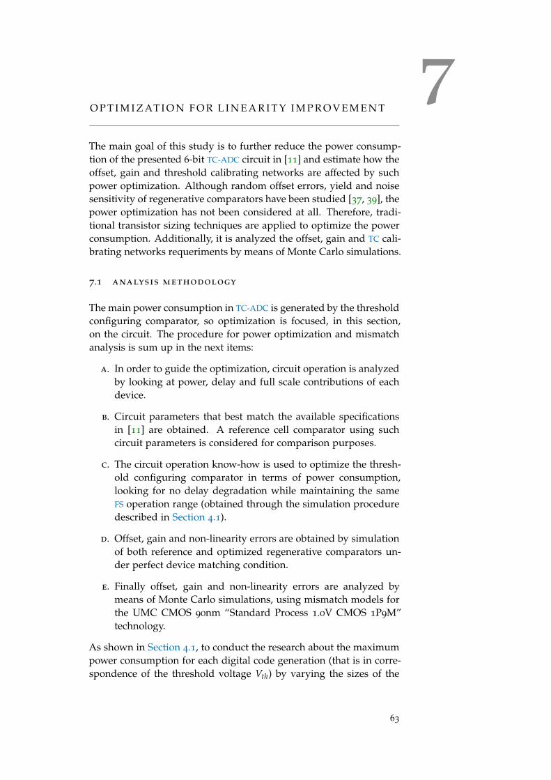
7O P T I M I Z AT I O N F O R L I N E A R I T Y I M P R O V E M E N T
The main goal of this study is to further reduce the power consump-tion of the presented 6-bit TC-ADC circuit in [11] and estimate how theoffset, gain and threshold calibrating networks are affected by suchpower optimization. Although random offset errors, yield and noisesensitivity of regenerative comparators have been studied [37, 39], thepower optimization has not been considered at all. Therefore, tradi-tional transistor sizing techniques are applied to optimize the powerconsumption. Additionally, it is analyzed the offset, gain and TC cali-brating networks requeriments by means of Monte Carlo simulations.
7.1 analysis methodology
The main power consumption in TC-ADC is generated by the thresholdconfiguring comparator, so optimization is focused, in this section,on the circuit. The procedure for power optimization and mismatchanalysis is sum up in the next items:
a. In order to guide the optimization, circuit operation is analyzedby looking at power, delay and full scale contributions of eachdevice.
b. Circuit parameters that best match the available specificationsin [11] are obtained. A reference cell comparator using suchcircuit parameters is considered for comparison purposes.
c. The circuit operation know-how is used to optimize the thresh-old configuring comparator in terms of power consumption,looking for no delay degradation while maintaining the sameFS operation range (obtained through the simulation proceduredescribed in Section 4.1).
d. Offset, gain and non-linearity errors are obtained by simulationof both reference and optimized regenerative comparators un-der perfect device matching condition.
e. Finally offset, gain and non-linearity errors are analyzed bymeans of Monte Carlo simulations, using mismatch models forthe UMC CMOS 90nm “Standard Process 1.0V CMOS 1P9M”technology.
As shown in Section 4.1, to conduct the research about the maximumpower consumption for each digital code generation (that is in corre-spondence of the threshold voltage Vth) by varying the sizes of the
63
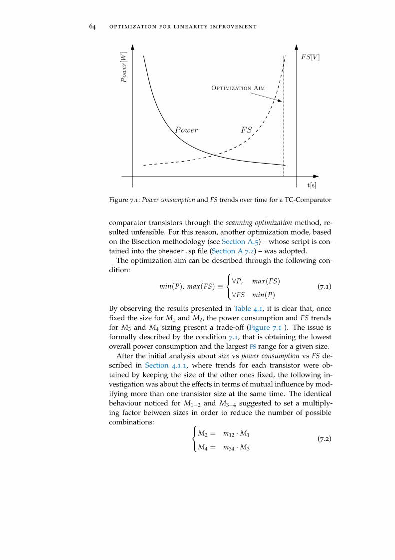
64 optimization for linearity improvement
Pow
er[W
]
FS[V ]
t[s]
Power FS
Optimization Aim
Figure 7.1: Power consumption and FS trends over time for a TC-Comparator
comparator transistors through the scanning optimization method, re-sulted unfeasible. For this reason, another optimization mode, basedon the Bisection methodology (see Section A.5) – whose script is con-tained into the oheader.sp file (Section A.7.2) – was adopted.
The optimization aim can be described through the following con-dition:
min(P), max(FS) ≡
∀P, max(FS)
∀FS min(P)(7.1)
By observing the results presented in Table 4.1, it is clear that, oncefixed the size for M1 and M2, the power consumption and FS trendsfor M3 and M4 sizing present a trade-off (Figure 7.1 ). The issue isformally described by the condition 7.1, that is obtaining the lowestoverall power consumption and the largest FS range for a given size.
After the initial analysis about size vs power consumption vs FS de-scribed in Section 4.1.1, where trends for each transistor were ob-tained by keeping the size of the other ones fixed, the following in-vestigation was about the effects in terms of mutual influence by mod-ifying more than one transistor size at the same time. The identicalbehaviour noticed for M1−2 and M3−4 suggested to set a multiply-ing factor between sizes in order to reduce the number of possiblecombinations: M2 = m12 ·M1
M4 = m34 ·M3
(7.2)
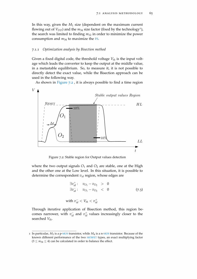
7.1 analysis methodology 65
In this way, given the M1 size (dependent on the maximum currentflowing out of VDD) and the m34 size factor (fixed by the technology1),the search was limited to finding m12 in order to minimize the powerconsumption and m34 to maximize the FS.
7.1.1 Optimization analysis by Bisection method
Given a fixed digital code, the threshold voltage Vth is the input volt-age which leads the converter to keep the output at the middle value,in a metastable equilibrium. So, to measure it, it is not possible todirectly detect the exact value, while the Bisection approach can beused in the following way.
As shown in Figure 7.2 , it is always possible to find a time region
Reset
O1
O2
HL
LL
∆t
V
t
10%
10%
Stable output values Region
Figure 7.2: Stable region for Output values detection
where the two output signals O1 and O2 are stable, one at the Highand the other one at the Low level. In this situation, it is possible todetermine the correspondent vid region, whose edges are
∃v+id : vO1 − vO2 > 0
∃v−id : vO1 − vO2 < 0 (7.3)
with v−id < Vth < v+id
Through iterative application of Bisection method, this region be-comes narrower, with v−id and v+id values increasingly closer to thesearched Vth.
1 In particular, M3 is a p-MOS transistor, while M4 is a n-MOS transistor. Because of theknown different performance of the two MOSFET types, an exact multiplying factor(3 ≤ m34 ≤ 4) can be calculated in order to balance the effect.
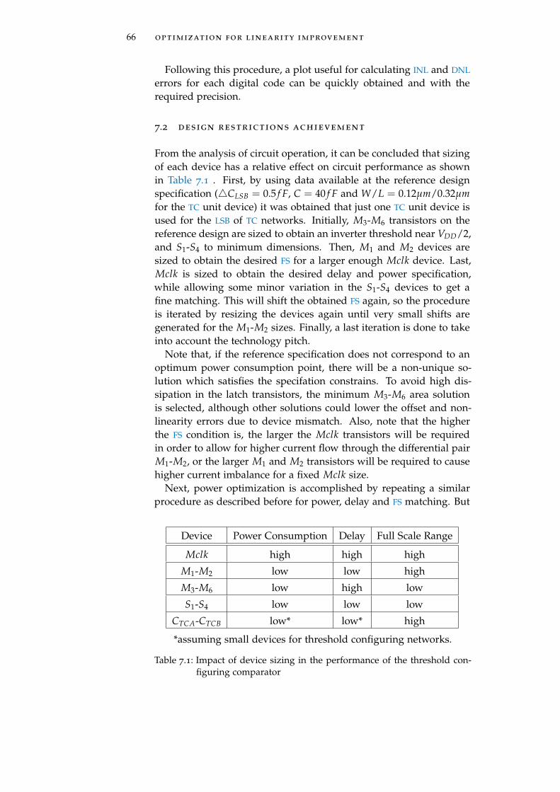
66 optimization for linearity improvement
Following this procedure, a plot useful for calculating INL and DNL
errors for each digital code can be quickly obtained and with therequired precision.
7.2 design restrictions achievement
From the analysis of circuit operation, it can be concluded that sizingof each device has a relative effect on circuit performance as shownin Table 7.1 . First, by using data available at the reference designspecification (4CLSB = 0.5 f F, C = 40 f F and W/L = 0.12µm/0.32µmfor the TC unit device) it was obtained that just one TC unit device isused for the LSB of TC networks. Initially, M3-M6 transistors on thereference design are sized to obtain an inverter threshold near VDD/2,and S1-S4 to minimum dimensions. Then, M1 and M2 devices aresized to obtain the desired FS for a larger enough Mclk device. Last,Mclk is sized to obtain the desired delay and power specification,while allowing some minor variation in the S1-S4 devices to get afine matching. This will shift the obtained FS again, so the procedureis iterated by resizing the devices again until very small shifts aregenerated for the M1-M2 sizes. Finally, a last iteration is done to takeinto account the technology pitch.
Note that, if the reference specification does not correspond to anoptimum power consumption point, there will be a non-unique so-lution which satisfies the specifation constrains. To avoid high dis-sipation in the latch transistors, the minimum M3-M6 area solutionis selected, although other solutions could lower the offset and non-linearity errors due to device mismatch. Also, note that the higherthe FS condition is, the larger the Mclk transistors will be requiredin order to allow for higher current flow through the differential pairM1-M2, or the larger M1 and M2 transistors will be required to causehigher current imbalance for a fixed Mclk size.
Next, power optimization is accomplished by repeating a similarprocedure as described before for power, delay and FS matching. But
Device Power Consumption Delay Full Scale Range
Mclk high high high
M1-M2 low low high
M3-M6 low high low
S1-S4 low low low
CTCA-CTCB low* low* high
*assuming small devices for threshold configuring networks.
Table 7.1: Impact of device sizing in the performance of the threshold con-figuring comparator

7.3 nonlinearity analysis : dnl and inl errors 67
in this case power specification is reduced to its minimum value. Min-imum power consumption can be determined by initially making M1-M2 devices large enough, and reducing the size of Mclk till delay andFS conditions are met. To avoid highly non-linear behavior, Mclk can-not be too much reduced in comparison with M1 and M2. On theother hand, as lower the M3/M5 (or M4/M6) ratio is, the smaller willbe the required Mclk devices. Thus, optimum power sizing tends toreduce M3/M5 and M4/M6 ratios and slighlty increase the M1/Mclkand M2/Mclk ones.
The sizing of TC units in the reference design allows for increasedCon/Co f f ratio (approximately 6 times) when compared with mini-mum size devices. On the one hand, high capacitive deltas in TC
networks relax the sizing condition of Mclk to fit the FS specificationand could reduce the power consumption. But on the other hand, itis preferrable to keep devices close to the minimum size in order toreduce the overall capacitive load, except for the case that reduceddevice mismatch is required. The obtained device sizing for TC unitsis considered a good compromise between Con/Co f f ratio, mismatchand impact on power consumption.
Both, in the reference design and in the optimized one, we as-sumed that the matching of power and delay constrains are met forinput differential voltages at ±10µV from the zero threshold condi-tion (TCA = TCB = 0). A common mode input voltage of 0.3V isalso assumed in the INA-INB terminals, because this is an optimumdesign point for the speed and yield [37] performance of latch-typevoltage sense amplifiers.
7.3 nonlinearity analysis : dnl and inl errors
Once the threshold voltage Vth,#n has been individuated for each #ndigital code (through Scanning optimization mode, as described inSection 4.1), it is possible to plot the real behavior of the TC-Comparator(Figure 7.3)

68 optimization for linearity improvement
Output Code#1 #2 #3 #4#0
Vth,#0
Vth,#1
Vth,#2
Vth,#3
FS ≡ Vth,#4
v id[V
]
Linear Behaviour
INL
Note that ideal linear behaviour of comparator is traced by drawinga straight line through zero and FS.
Figure 7.3: Qualitative plot of non-linear relationship between Input voltageand Output digital code for a TC-Comparator
and compare it with the ideal linear working function. From thiscomparation it is obtained the INL error, that is the deviation of theoutput code from the linear trend (as defined in Section 1.2.2).
The same graph is also useful for obtaining and evaluating the DNL
error of each digital code, calculated through Equation 1.3.
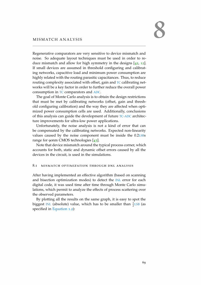
8M I S M AT C H A N A LY S I S
Regenerative comparators are very sensitive to device mismatch andnoise. So adequate layout techniques must be used in order to re-duce mismatch and allow for high symmetry in the designs [42, 12].If small devices are assumed in threshold configuring and calibrat-ing networks, capacitive load and minimum power consumption arehighly related with the routing parasitic capacitances. Thus, to reducerouting complexity associated with offset, gain and TC calibrating net-works will be a key factor in order to further reduce the overall powerconsumption in TC comparators and ADC.
The goal of Monte Carlo analysis is to obtain the design restrictionsthat must be met by calibrating networks (offset, gain and thresh-old configuring calibration) and the way they are affected when opti-mized power consumption cells are used. Additionally, conclusionsof this analysis can guide the development of future TC-ADC architec-ture improvements for ultra-low power applications.
Unfortunately, the noise analysis is not a kind of error that canbe compensated by the calibrating networks. Expected non-linearityvalues caused by the noise component must be inside the 0.2LSBsrange for 90nm CMOS technologies [43].
Note that device mismatch around the typical process corner, whichaccounts for both, static and dynamic offset errors caused by all thedevices in the circuit, is used in the simulations.
8.1 mismatch optimization through dnl analysis
After having implemented an effective algorithm (based on scanningand bisection optimization modes) to detect the INL error for eachdigital code, it was used time after time through Monte Carlo simu-lations, which permit to analyze the effects of process scattering overthe observed parameters.
By plotting all the results on the same graph, it is easy to spot thebiggest INL (absolute) value, which has to be smaller than 1
2 LSB (asspecified in Equation 1.2):
69
70 mismatch analysis
0000 0001 1111 Code
INL
+1LSB
−1LSB
+ 12LSB
+ 12LSB
Figure 8.1: Qualitative plot of INL errors for each digital code generatedthrough Monte Carlo simulations

9R E S U LT S
All the circuit parameters and performance obtained are presented inTable 9.1 and Table 9.2 for the reference design (REF) and the poweroptimized one (OPT) respectively. Circuit parameters are shown inTable 9.1, in terms of transistor size, while circuit performance isshown in Table 9.2 in terms of delay, power and FS range, and themaximum absolute offset, gain and non-linearity (DNL, INL) errorsfor all the possible threshold configuring TCA and TCB words. Ascommented before, power and delay measurements are referred toa ±10µV input signal for the TCA = TCB = 0 codes. A resolutionstep of 100µV (about 0.02 LSBs) is used for the voltage sweep and acommon mode input voltage of 0.3V is assumed at the INA-INB ter-minals. The best-fit of the trip points to a straight line obtained by theleast squares method is assumed for linearity parameters (offset, gain,DNL and INL). The sampling period is fixed at 40ns, in order to avoidnon-linear power behavior near the maximum sampling frequency(50MSps).
It can be observed that the optimized design reduces the power con-sumption and delay of more than 77% and 20% respectively, for a fullscale range of ±160mV. Moreover, our power optimized design ex-hibits near 50% improvement for the linearity error parameters. Thehigher energy efficiency of the optimized solution delivers energy tothe capacitor arrays in a more efficient way than the reference solu-tion did. As lower energy is dissipated by the internal devices incomparison with the quantity distributed to capacitor arrays, lowernon-linear effects are obtained. Non-linearity errors for each TC codeare shown in Figure 9.1. Note that, due to perfect simmetry in thedesign, the INL error for TCA = TCB = 0 (code number 31) is null.
Finally, mismatch analysis results are presented in Table 9.3 . Itcan be observed that the maximum absolute offset errors of both de-signs are close to each other. But the optimized power consumptionversion achieves more than 30% gain and DNL errors reduction. Thelower gain error can be directly used for decreasing the correspond-ing calibrating network size (and complexity) and to further reducethe power consumption. On the other hand the INL error is about21% worse for the power optimized design. The INL error increase isdue to the higher relative variations of the node currents in presenceof a mismatch condition when reducing the device size.
Figure 9.2 plots the INL errors corresponding to each code andMonte Carlo run. 3D plots are shown in Figure 9.2a and Figure 9.2b.Overlayed 2D plots for each run are shown in Figure 9.2c and Fig-
71

72 results
Device Size (REF) Size (OPT)
Mclk 41.13µm× 0.08µm 2.69µm× 0.08µm
M1, M2 2.79µm× 0.08µm 4.18µm× 0.08µm
M3, M6 0.13µm× 0.08µm 0.40µm× 0.08µm
S1, S4 1.22µm× 0.08µm 1.70µm× 0.08µm
CTCA , CTCB(LSB) 0.12µm× 0.32µm 0.12µm× 0.32µm
Table 9.1: Device sizing parameters for reference (REF) and optimized (OPT)comparators
Device REF OPT
Power[µW] 13.00 2.92
Delay[ns] 1.65 1.31
FS[mV] ±159.95 ±160.10
Offset[mV] −3.11 −1.5
Gain Error[%] +2.00 −0.98
DNL[LSBs] ±0.118 ±0.071
INL[LSBs] ±0.639 ±0.338
Table 9.2: Obtained performance for reference (REF) and optimized (OPT)comparators, without device mismatch
Device REF OPT
Offset[mV] ±93.60 ±91.25
Gain Error[%] ±8.54 ±5.40
DNL[LSBs] ±0.124 ±0.085
INL[LSBs] ±0.956 ±1.163
Table 9.3: Obtained performance for reference (REF) and optimized (OPT)comparators, with device mismatch
results 73
ure 9.2d. The offset and gain erros are depicted in Figure 9.3. Al-though the INL error is about 0.2 LSBs worse for the power optimizeddesign it can be more easily modeled than the reference ones. Thiscould be used to simplify the required calibration parameters in thecase, for example, of a memory-based cancellation scheme.
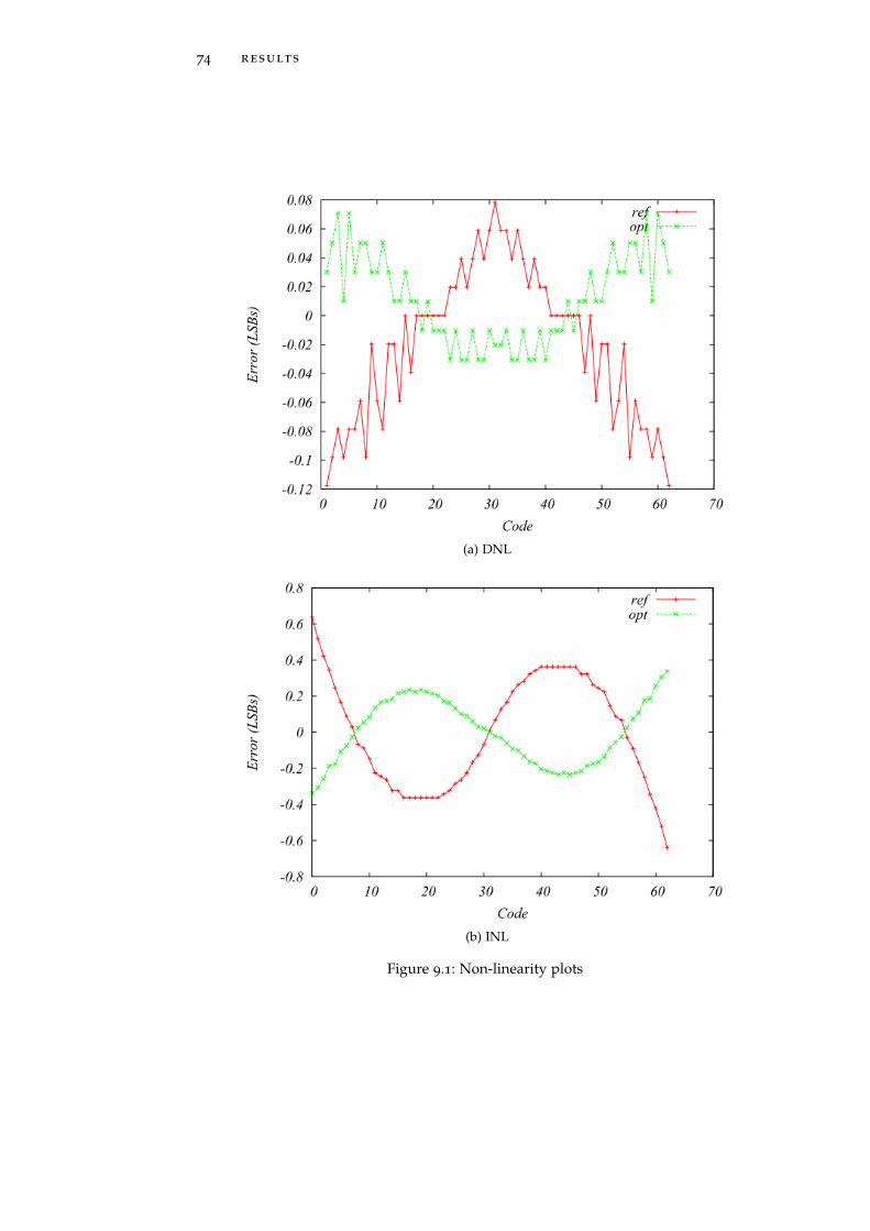
74 results
(a) DNL
(b) INL
Figure 9.1: Non-linearity plots
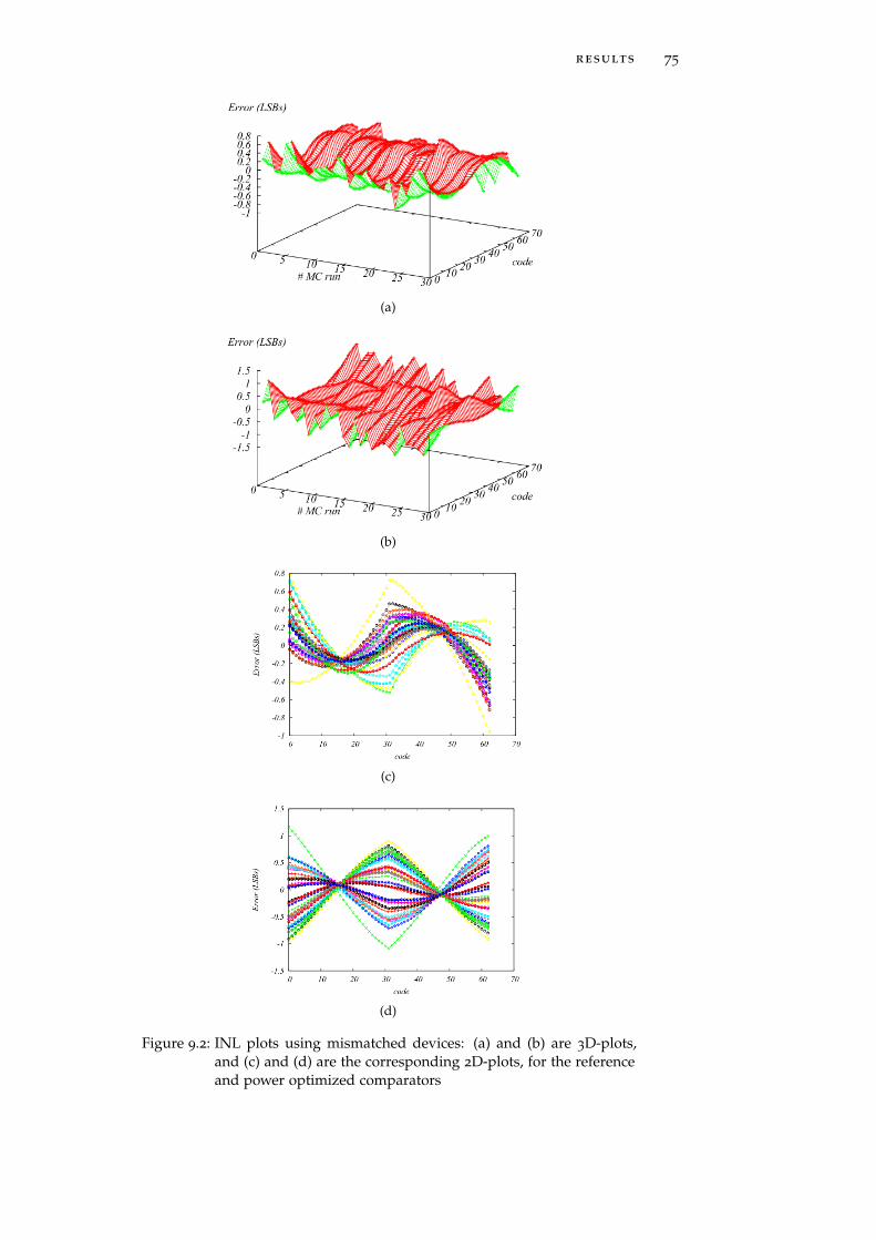
results 75
(a)
(b)
(c)
(d)
Figure 9.2: INL plots using mismatched devices: (a) and (b) are 3D-plots,and (c) and (d) are the corresponding 2D-plots, for the referenceand power optimized comparators

76 results
(a)
(b)
(c)
(d)
Figure 9.3: INL plots using mismatched devices: (a) and (b) are 3D-plots,and (c) and (d) are the corresponding 2D-plots, for the referenceand power optimized comparators
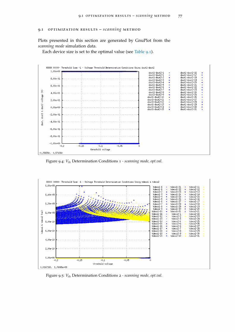
9.1 optimization results – scanning method 77
9.1 optimization results – scanning method
Plots presented in this section are generated by GnuPlot from thescanning mode simulation data.
Each device size is set to the optimal value (see Table 9.1).
Figure 9.4: Vth Determination Conditions 1 - scanning mode, opt.val.
Figure 9.5: Vth Determination Conditions 2 - scanning mode, opt.val.
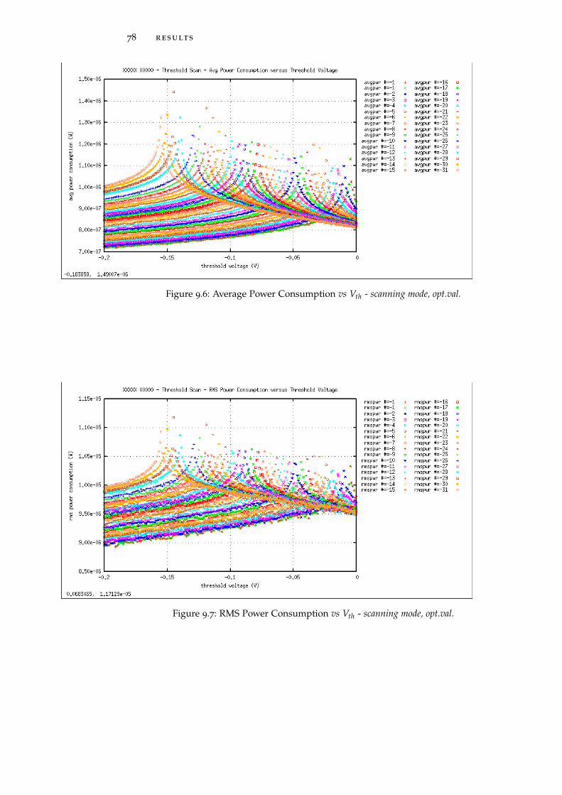
78 results
Figure 9.6: Average Power Consumption vs Vth - scanning mode, opt.val.
Figure 9.7: RMS Power Consumption vs Vth - scanning mode, opt.val.
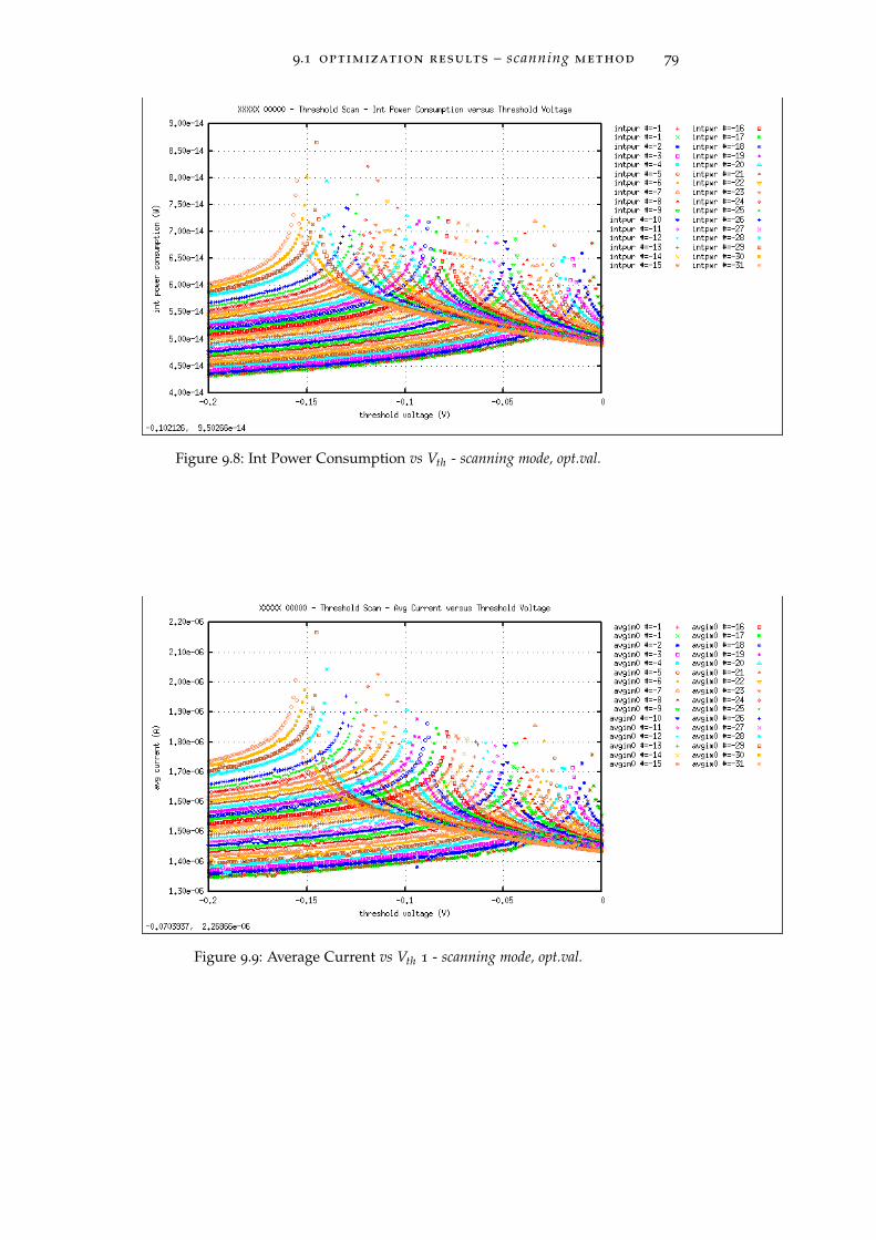
9.1 optimization results – scanning method 79
Figure 9.8: Int Power Consumption vs Vth - scanning mode, opt.val.
Figure 9.9: Average Current vs Vth 1 - scanning mode, opt.val.
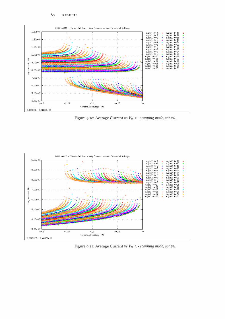
80 results
Figure 9.10: Average Current vs Vth 2 - scanning mode, opt.val.
Figure 9.11: Average Current vs Vth 3 - scanning mode, opt.val.
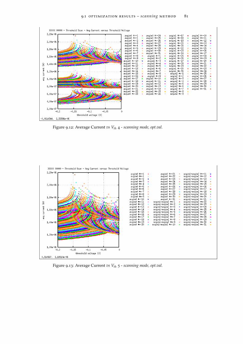
9.1 optimization results – scanning method 81
Figure 9.12: Average Current vs Vth 4 - scanning mode, opt.val.
Figure 9.13: Average Current vs Vth 5 - scanning mode, opt.val.
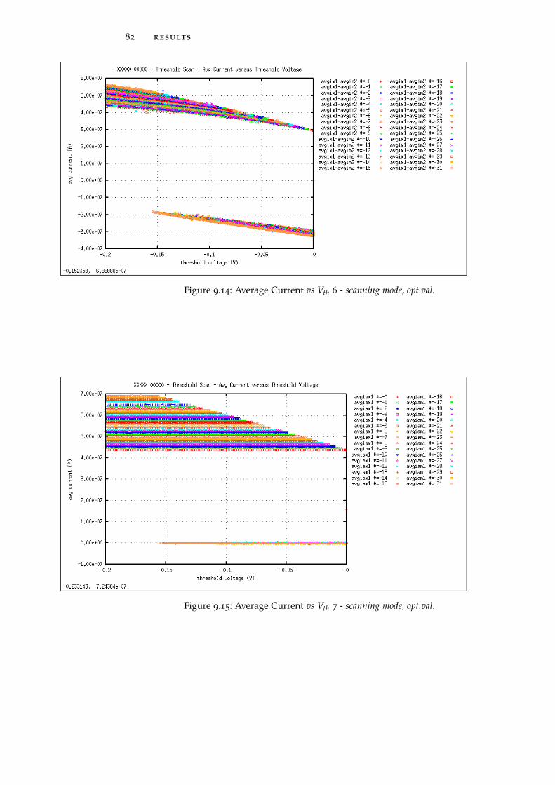
82 results
Figure 9.14: Average Current vs Vth 6 - scanning mode, opt.val.
Figure 9.15: Average Current vs Vth 7 - scanning mode, opt.val.

9.1 optimization results – scanning method 83
Figure 9.16: Average Current vs Vth 8 - scanning mode, opt.val.
Figure 9.17: RMS Current vs Vth 1 - scanning mode, opt.val.
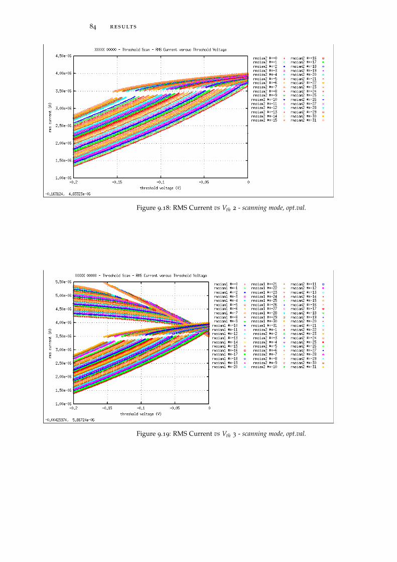
84 results
Figure 9.18: RMS Current vs Vth 2 - scanning mode, opt.val.
Figure 9.19: RMS Current vs Vth 3 - scanning mode, opt.val.

9.1 optimization results – scanning method 85
Figure 9.20: Int Current vs Vth 1 - scanning mode, opt.val.
Figure 9.21: Int Current vs Vth 2 - scanning mode, opt.val.
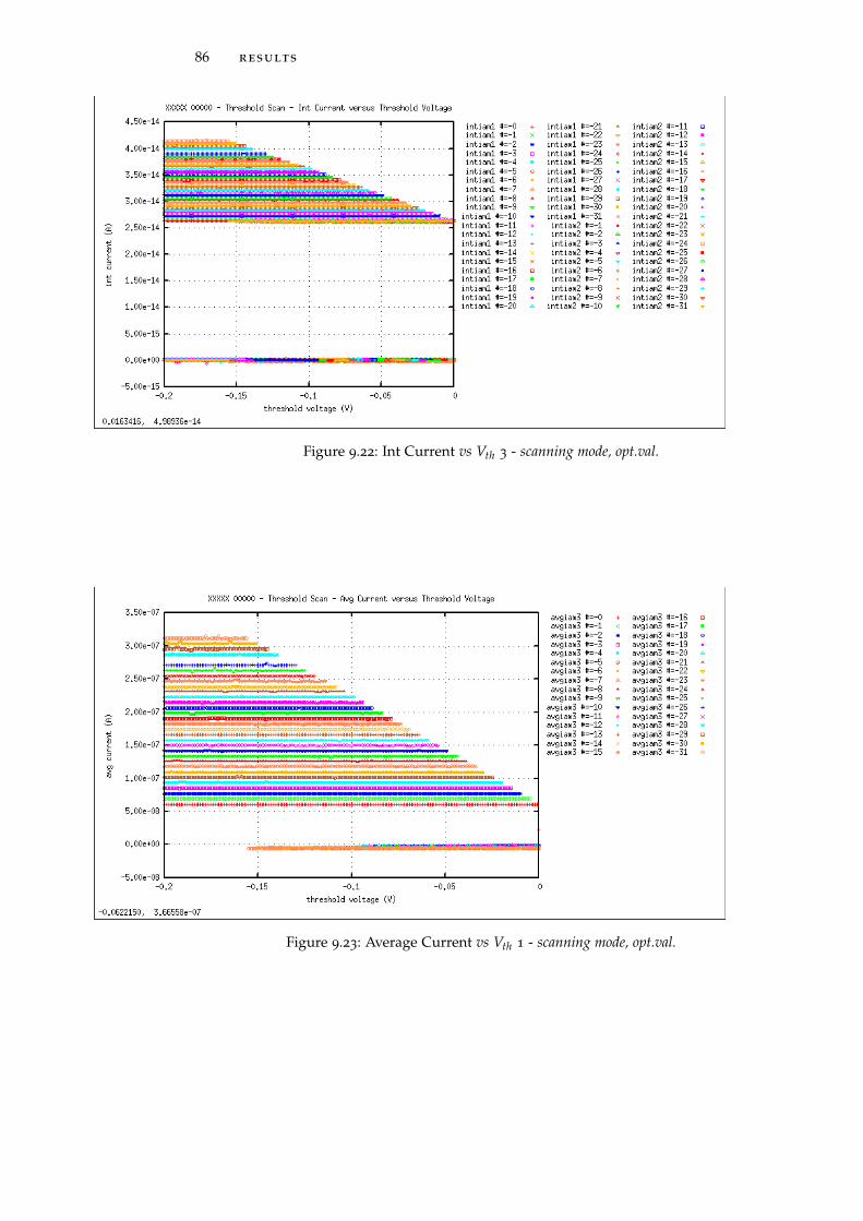
86 results
Figure 9.22: Int Current vs Vth 3 - scanning mode, opt.val.
Figure 9.23: Average Current vs Vth 1 - scanning mode, opt.val.

9.1 optimization results – scanning method 87
Figure 9.24: Average Current vs Vth 2 - scanning mode, opt.val.
Figure 9.25: RMS Current vs Vth 4 - scanning mode, opt.val.
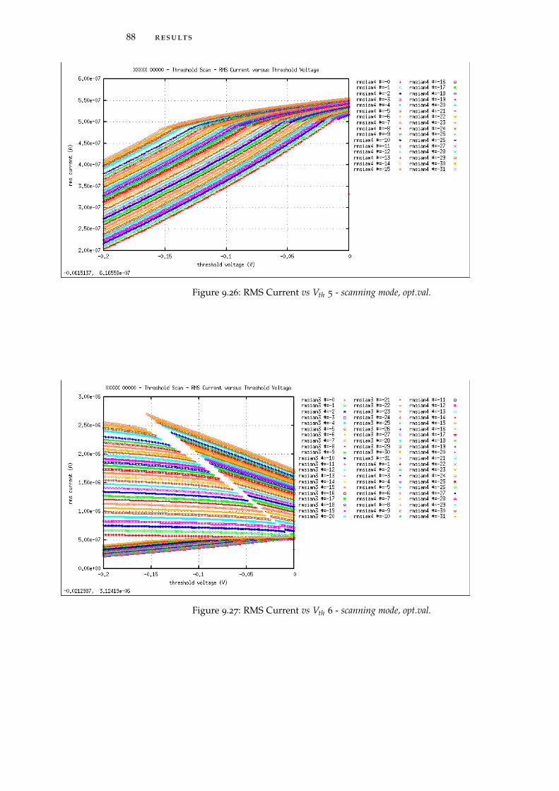
88 results
Figure 9.26: RMS Current vs Vth 5 - scanning mode, opt.val.
Figure 9.27: RMS Current vs Vth 6 - scanning mode, opt.val.
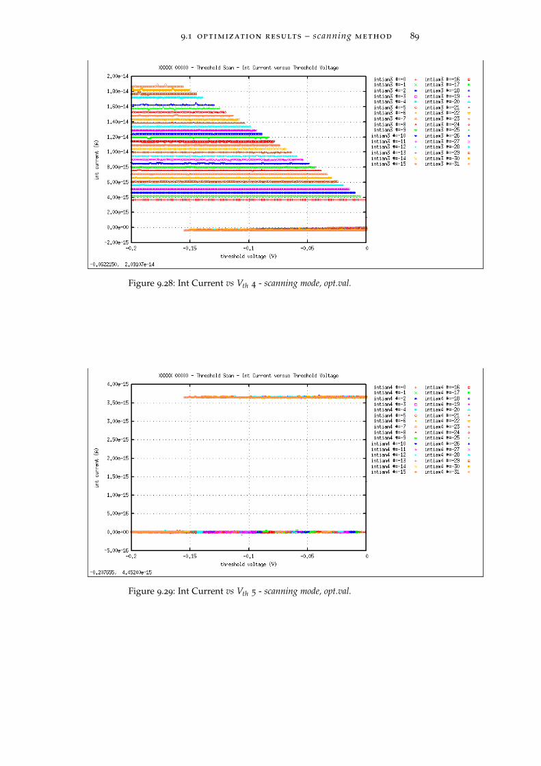
9.1 optimization results – scanning method 89
Figure 9.28: Int Current vs Vth 4 - scanning mode, opt.val.
Figure 9.29: Int Current vs Vth 5 - scanning mode, opt.val.
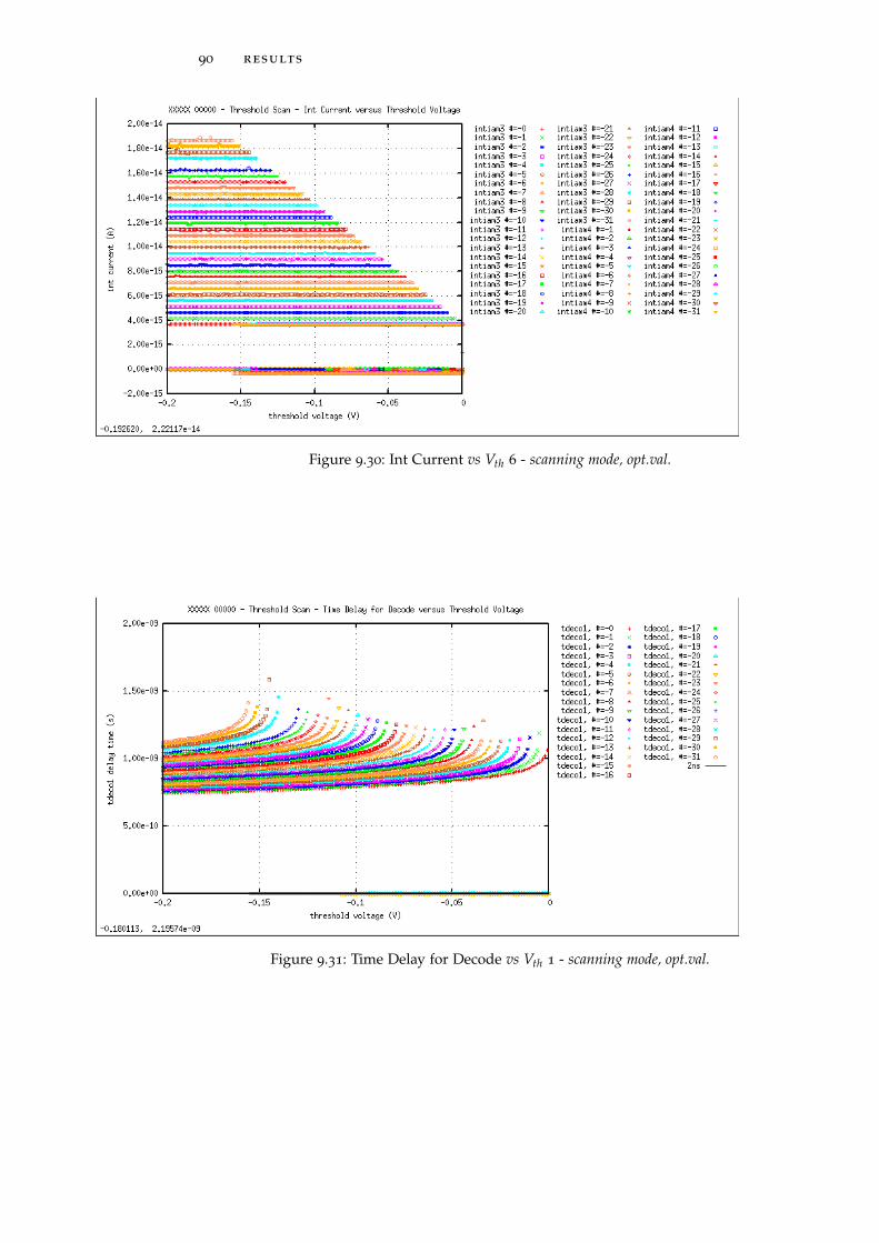
90 results
Figure 9.30: Int Current vs Vth 6 - scanning mode, opt.val.
Figure 9.31: Time Delay for Decode vs Vth 1 - scanning mode, opt.val.
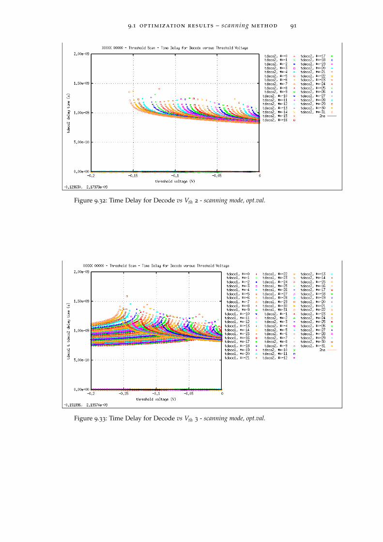
9.1 optimization results – scanning method 91
Figure 9.32: Time Delay for Decode vs Vth 2 - scanning mode, opt.val.
Figure 9.33: Time Delay for Decode vs Vth 3 - scanning mode, opt.val.

92 results
9.2 reference values – scanning method
Plots presented in this section are generated by GnuPlot from thescanning mode simulation data.
Each device size is set to the reference value (see Table 9.1).
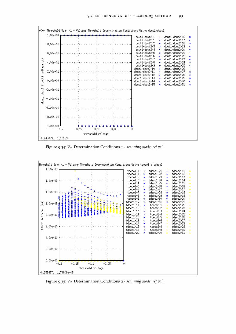
9.2 reference values – scanning method 93
Figure 9.34: Vth Determination Conditions 1 - scanning mode, ref.val.
Figure 9.35: Vth Determination Conditions 2 - scanning mode, ref.val.
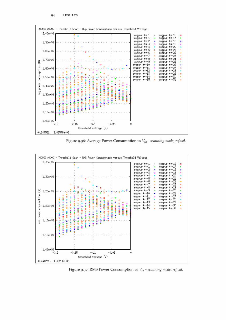
94 results
Figure 9.36: Average Power Consumption vs Vth - scanning mode, ref.val.
Figure 9.37: RMS Power Consumption vs Vth - scanning mode, ref.val.

9.2 reference values – scanning method 95
Figure 9.38: Int Power Consumption vs Vth - scanning mode, ref.val.
Figure 9.39: Average Current vs Vth 1 - scanning mode, ref.val.
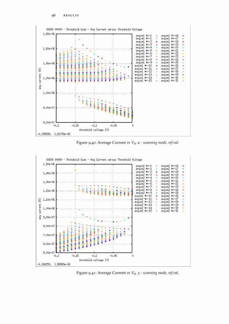
96 results
Figure 9.40: Average Current vs Vth 2 - scanning mode, ref.val.
Figure 9.41: Average Current vs Vth 3 - scanning mode, ref.val.
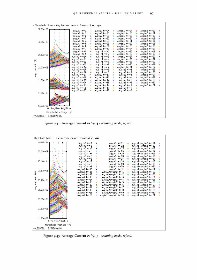
9.2 reference values – scanning method 97
Figure 9.42: Average Current vs Vth 4 - scanning mode, ref.val.
Figure 9.43: Average Current vs Vth 5 - scanning mode, ref.val.

98 results
Figure 9.44: Average Current vs Vth 6 - scanning mode, ref.val.
Figure 9.45: Average Current vs Vth 7 - scanning mode, ref.val.
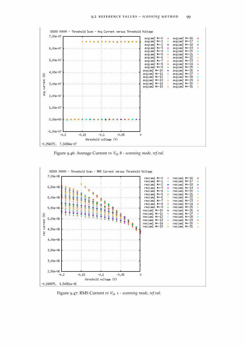
9.2 reference values – scanning method 99
Figure 9.46: Average Current vs Vth 8 - scanning mode, ref.val.
Figure 9.47: RMS Current vs Vth 1 - scanning mode, ref.val.
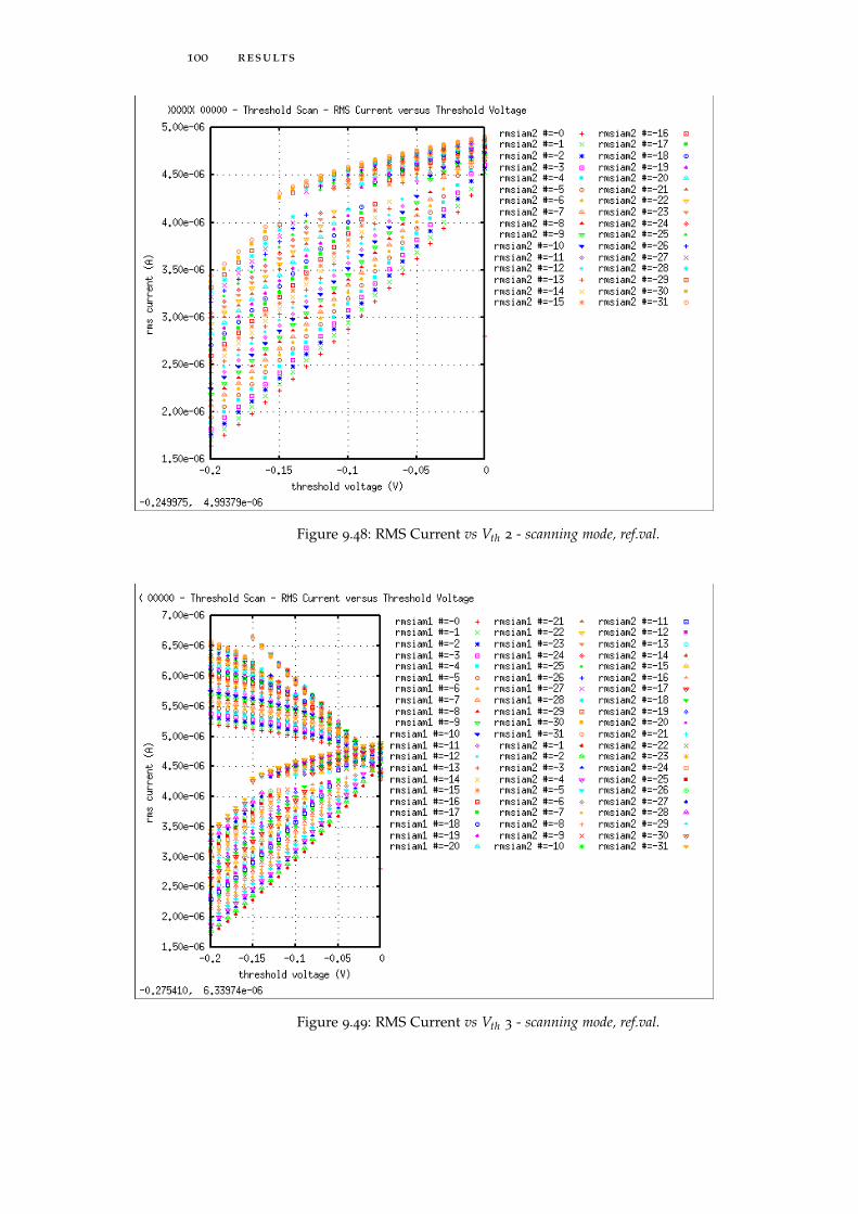
100 results
Figure 9.48: RMS Current vs Vth 2 - scanning mode, ref.val.
Figure 9.49: RMS Current vs Vth 3 - scanning mode, ref.val.
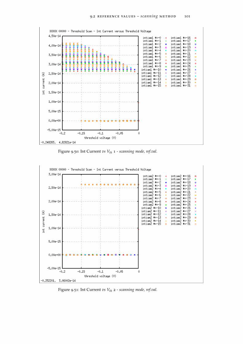
9.2 reference values – scanning method 101
Figure 9.50: Int Current vs Vth 1 - scanning mode, ref.val.
Figure 9.51: Int Current vs Vth 2 - scanning mode, ref.val.
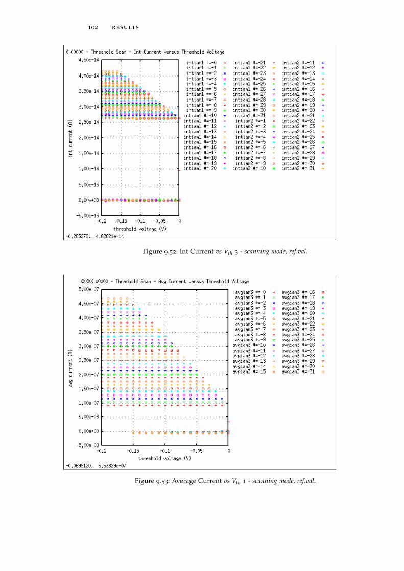
102 results
Figure 9.52: Int Current vs Vth 3 - scanning mode, ref.val.
Figure 9.53: Average Current vs Vth 1 - scanning mode, ref.val.
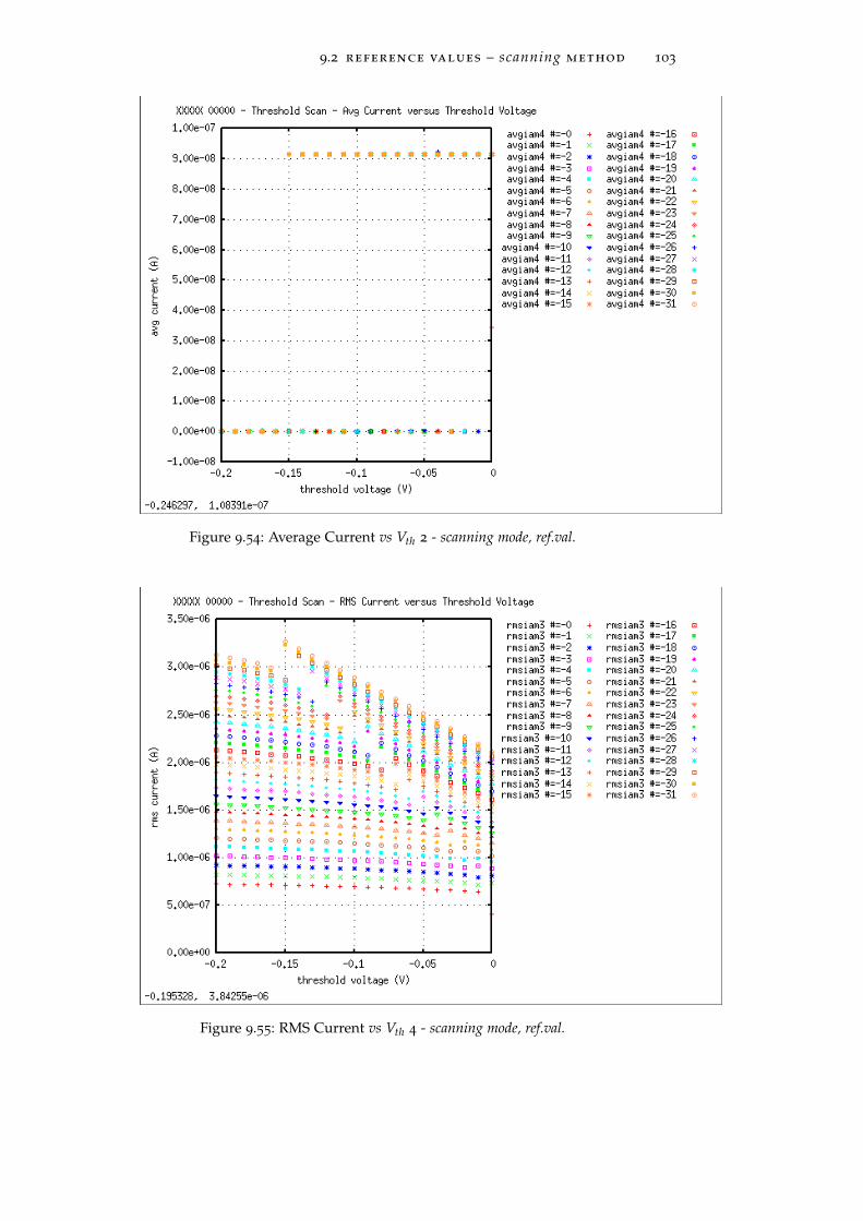
9.2 reference values – scanning method 103
Figure 9.54: Average Current vs Vth 2 - scanning mode, ref.val.
Figure 9.55: RMS Current vs Vth 4 - scanning mode, ref.val.
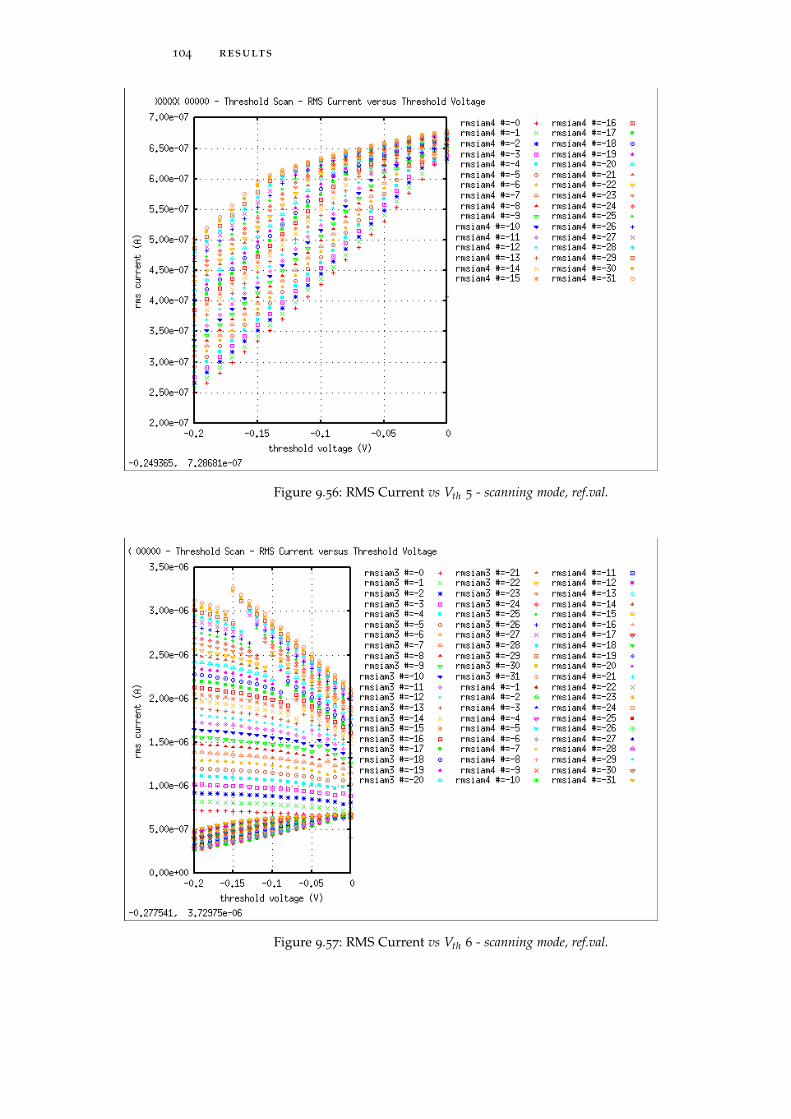
104 results
Figure 9.56: RMS Current vs Vth 5 - scanning mode, ref.val.
Figure 9.57: RMS Current vs Vth 6 - scanning mode, ref.val.
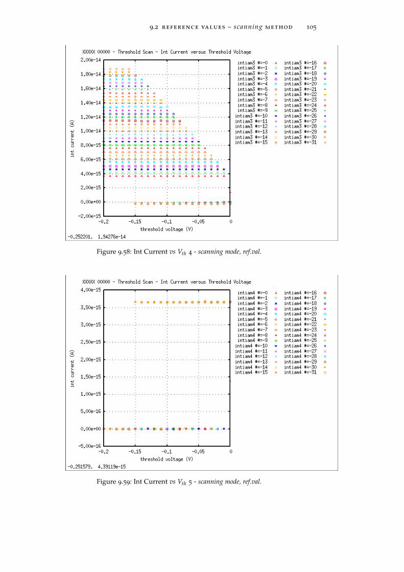
9.2 reference values – scanning method 105
Figure 9.58: Int Current vs Vth 4 - scanning mode, ref.val.
Figure 9.59: Int Current vs Vth 5 - scanning mode, ref.val.

106 results
Figure 9.60: Int Current vs Vth 6 - scanning mode, ref.val.
Figure 9.61: Time Delay for Decode vs Vth 1 - scanning mode, ref.val.
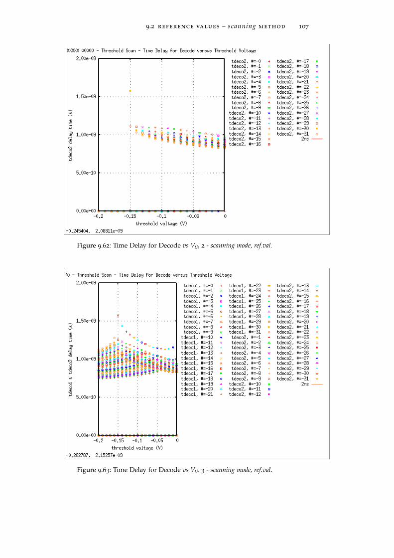
9.2 reference values – scanning method 107
Figure 9.62: Time Delay for Decode vs Vth 2 - scanning mode, ref.val.
Figure 9.63: Time Delay for Decode vs Vth 3 - scanning mode, ref.val.

108 results
9.3 mismatch results – monte carlo simulation
Plots presented in this section are generated by GnuPlot from MonteCarlo simulation data.
Each device size is set to the optimal value (see Table 9.1).

9.3 mismatch results – monte carlo simulation 109
Figure 9.64: Slope - mismatch, MonteCarlo EndPoint method
Figure 9.65: Offset - mismatch, MonteCarlo EndPoint method
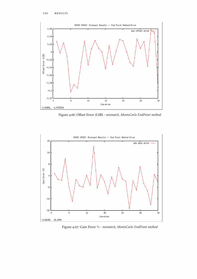
110 results
Figure 9.66: Offset Error (LSB) - mismatch, MonteCarlo EndPoint method
Figure 9.67: Gain Error % - mismatch, MonteCarlo EndPoint method
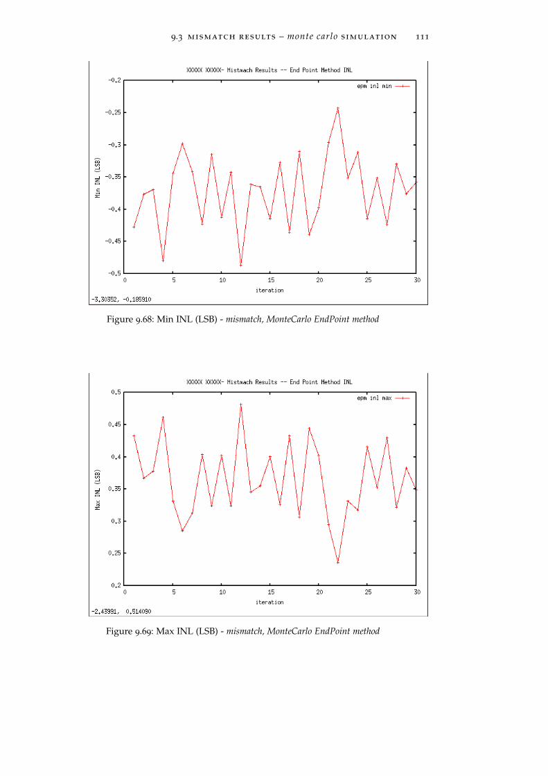
9.3 mismatch results – monte carlo simulation 111
Figure 9.68: Min INL (LSB) - mismatch, MonteCarlo EndPoint method
Figure 9.69: Max INL (LSB) - mismatch, MonteCarlo EndPoint method

112 results
Figure 9.70: Median INL (LSB) - mismatch, MonteCarlo EndPoint method
Figure 9.71: Mean INL (LSB) - mismatch, MonteCarlo EndPoint method

9.3 mismatch results – monte carlo simulation 113
Figure 9.72: Standard Deviation INL (LSB) - mismatch, MonteCarlo EndPointmethod
Figure 9.73: Sum INL (LSB) - mismatch, MonteCarlo EndPoint method
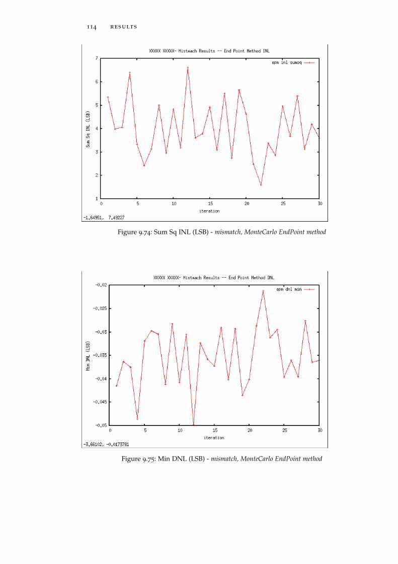
114 results
Figure 9.74: Sum Sq INL (LSB) - mismatch, MonteCarlo EndPoint method
Figure 9.75: Min DNL (LSB) - mismatch, MonteCarlo EndPoint method
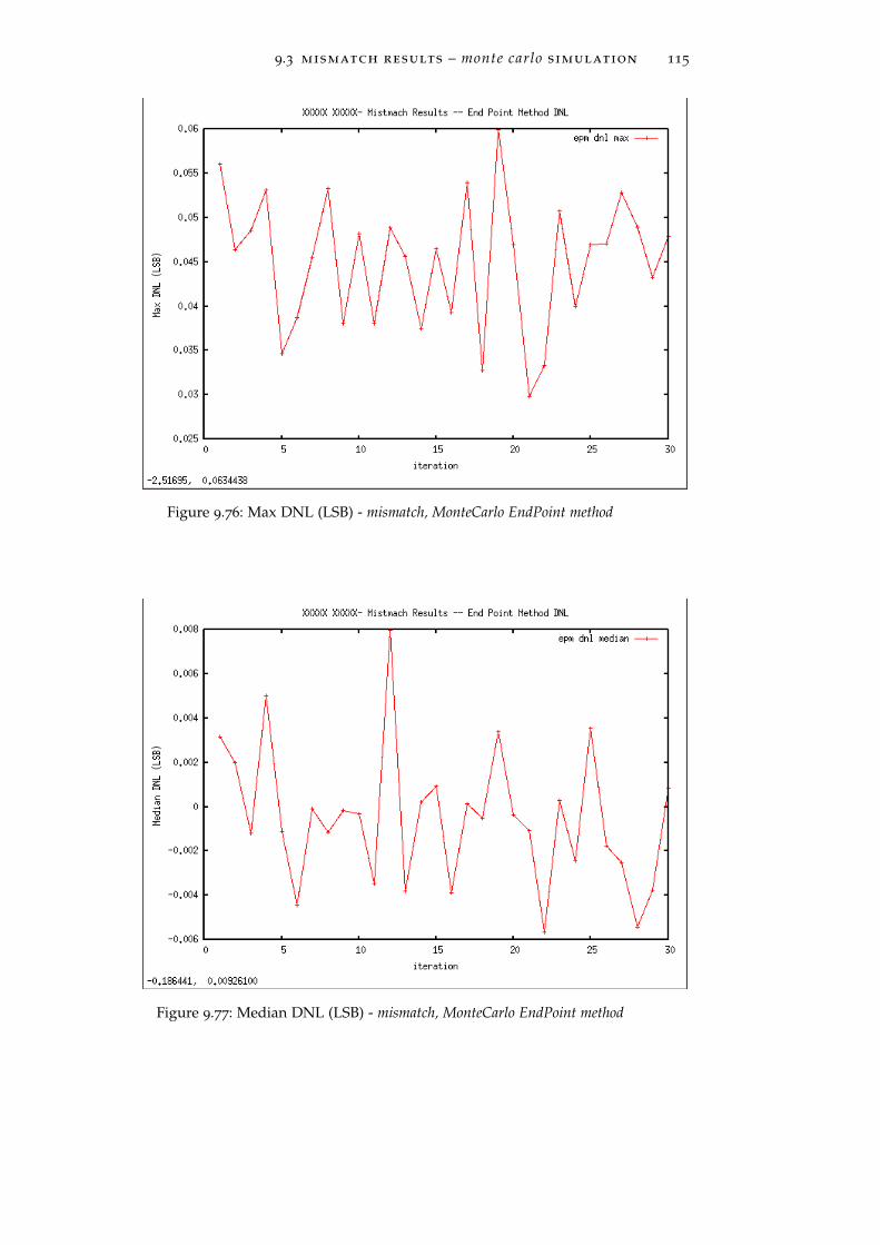
9.3 mismatch results – monte carlo simulation 115
Figure 9.76: Max DNL (LSB) - mismatch, MonteCarlo EndPoint method
Figure 9.77: Median DNL (LSB) - mismatch, MonteCarlo EndPoint method
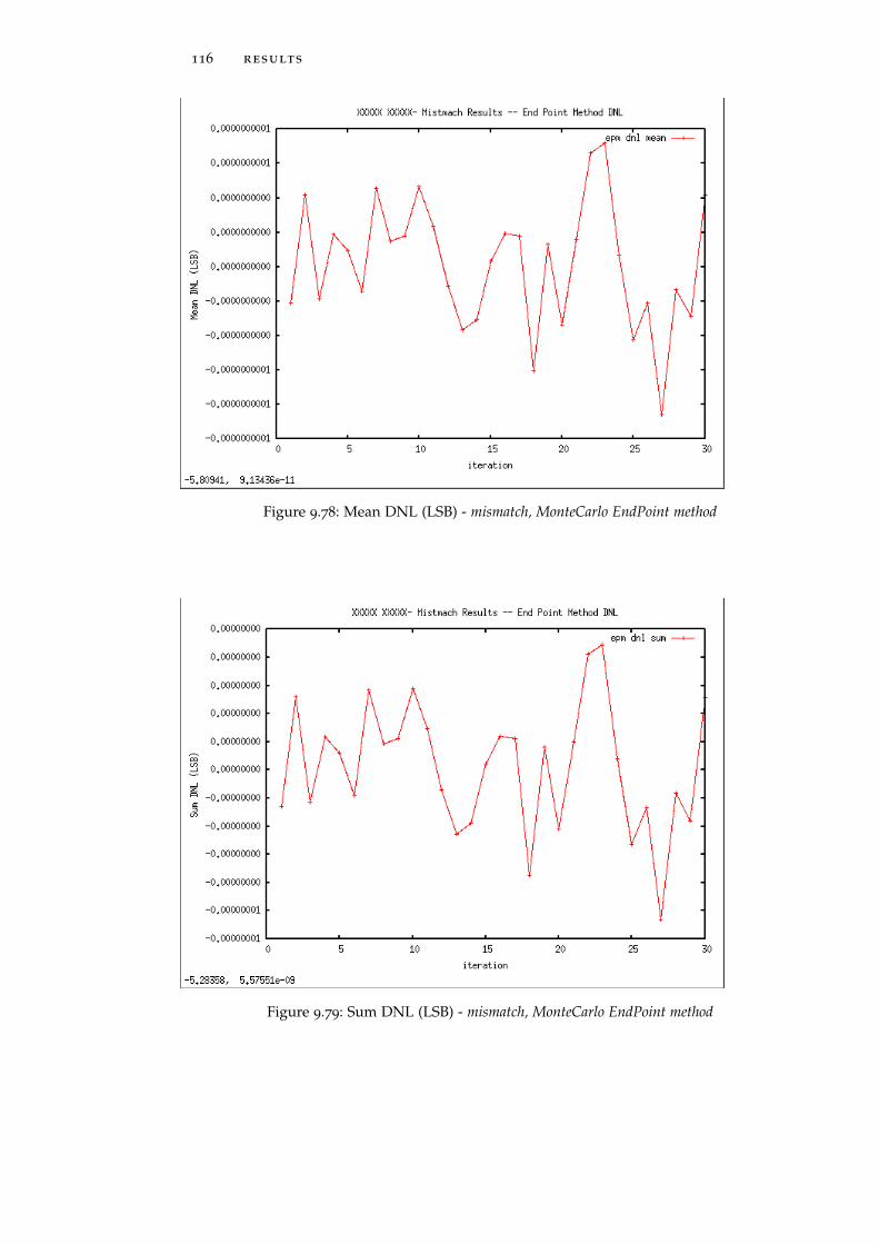
116 results
Figure 9.78: Mean DNL (LSB) - mismatch, MonteCarlo EndPoint method
Figure 9.79: Sum DNL (LSB) - mismatch, MonteCarlo EndPoint method
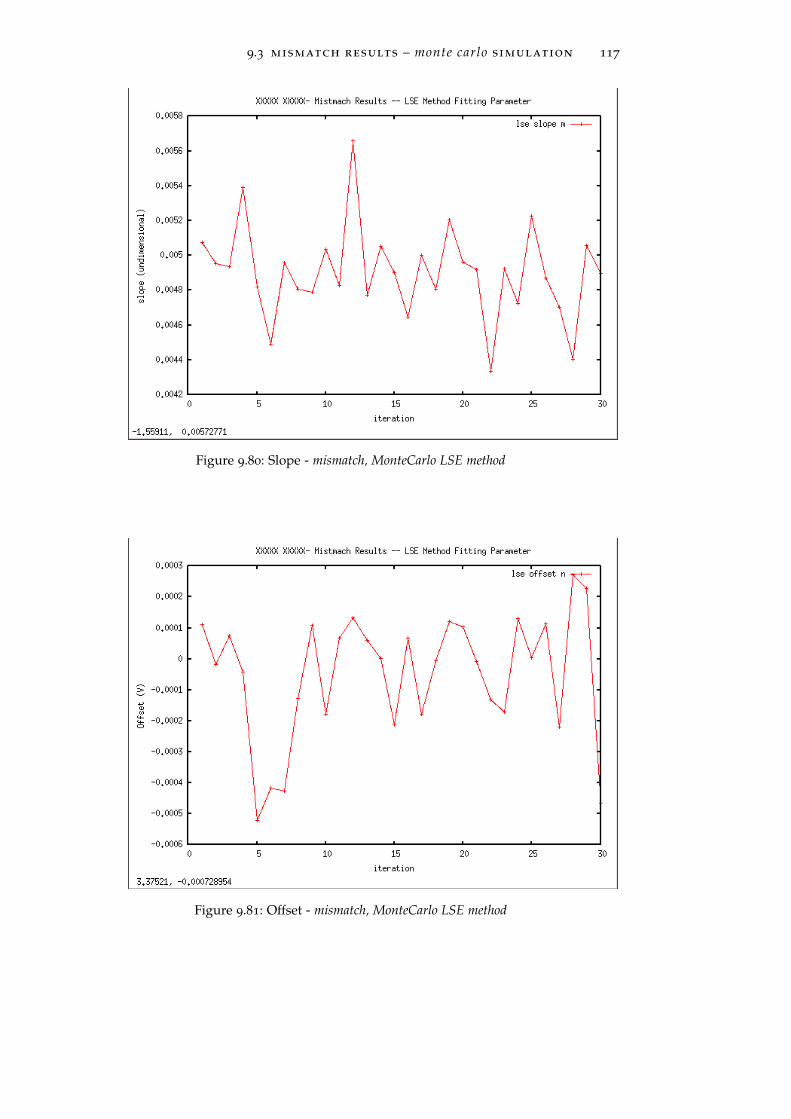
9.3 mismatch results – monte carlo simulation 117
Figure 9.80: Slope - mismatch, MonteCarlo LSE method
Figure 9.81: Offset - mismatch, MonteCarlo LSE method

118 results
Figure 9.82: Offset Error (LSB) - mismatch, MonteCarlo LSE method
Figure 9.83: Gain Error % - mismatch, MonteCarlo LSE method

9.3 mismatch results – monte carlo simulation 119
Figure 9.84: Min INL (LSB) - mismatch, MonteCarlo LSE method
Figure 9.85: Max INL (LSB) - mismatch, MonteCarlo LSE method
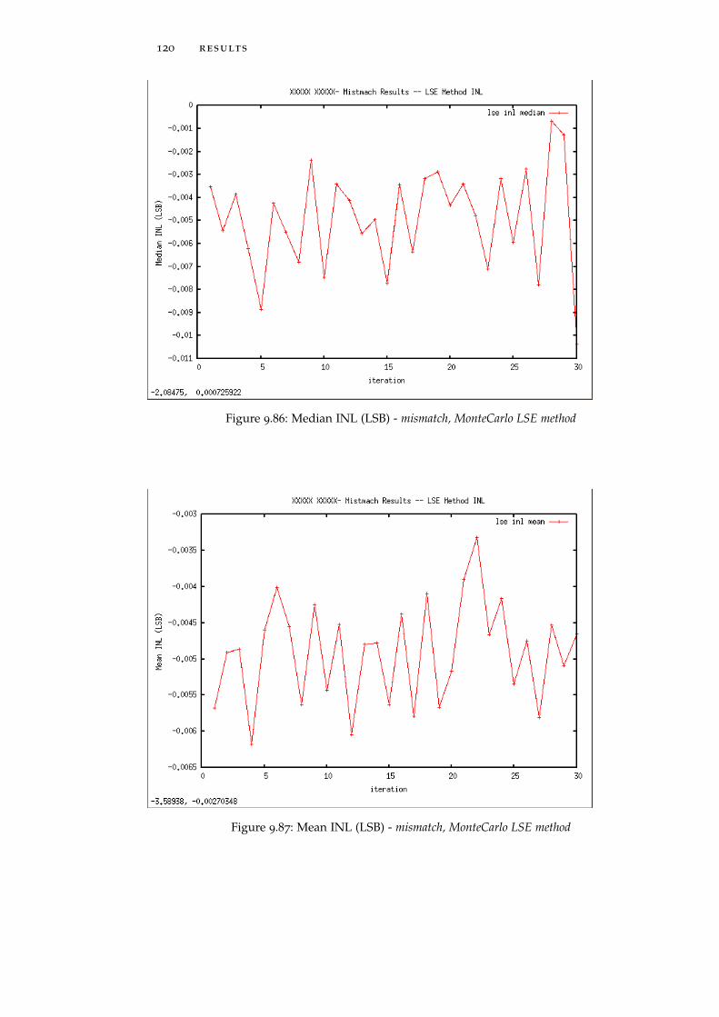
120 results
Figure 9.86: Median INL (LSB) - mismatch, MonteCarlo LSE method
Figure 9.87: Mean INL (LSB) - mismatch, MonteCarlo LSE method
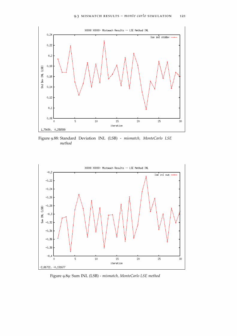
9.3 mismatch results – monte carlo simulation 121
Figure 9.88: Standard Deviation INL (LSB) - mismatch, MonteCarlo LSEmethod
Figure 9.89: Sum INL (LSB) - mismatch, MonteCarlo LSE method
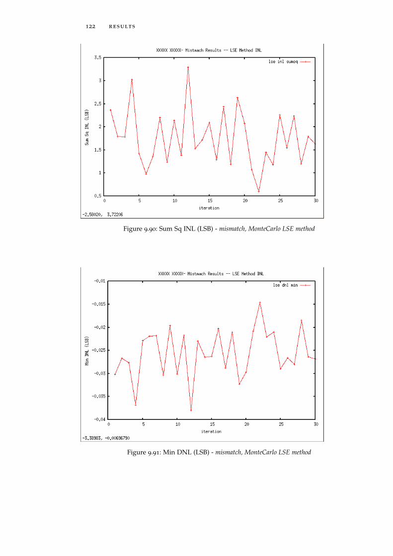
122 results
Figure 9.90: Sum Sq INL (LSB) - mismatch, MonteCarlo LSE method
Figure 9.91: Min DNL (LSB) - mismatch, MonteCarlo LSE method
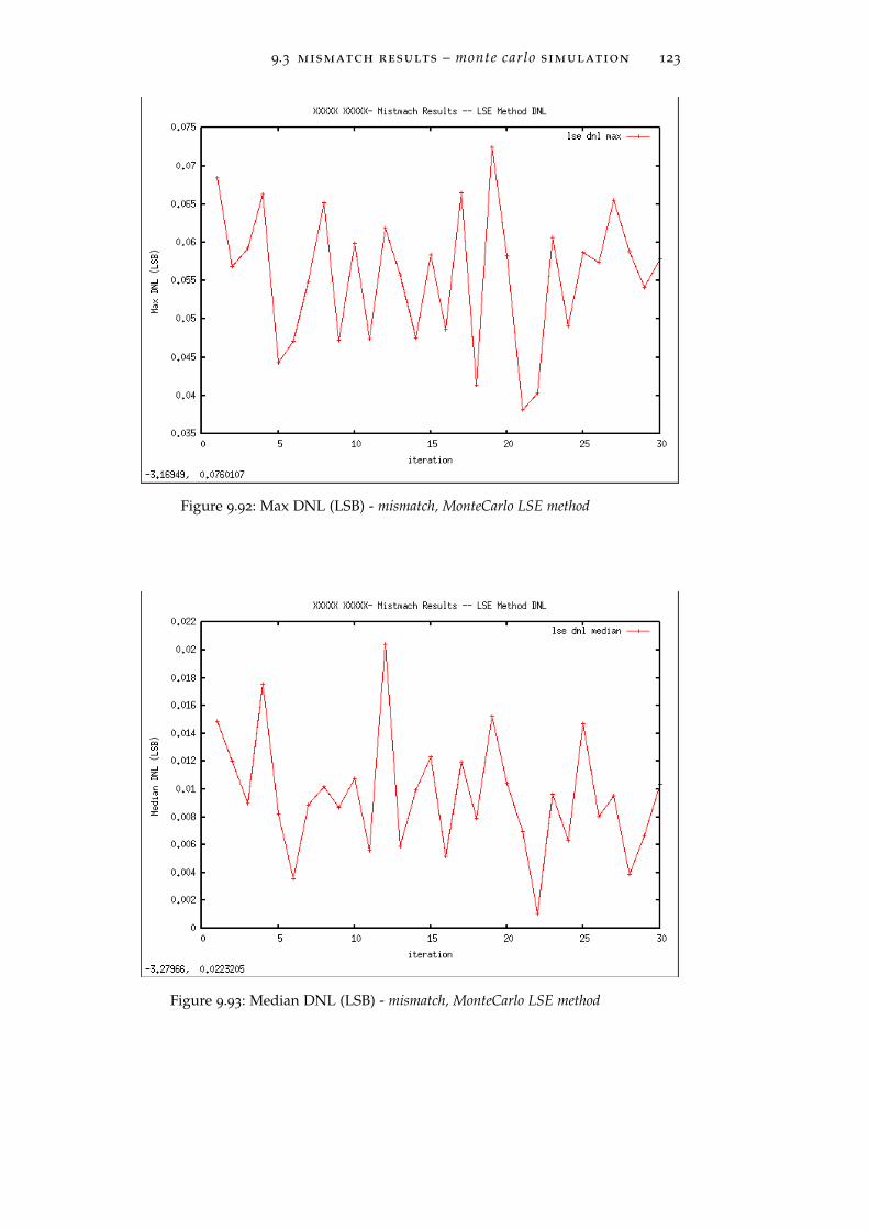
9.3 mismatch results – monte carlo simulation 123
Figure 9.92: Max DNL (LSB) - mismatch, MonteCarlo LSE method
Figure 9.93: Median DNL (LSB) - mismatch, MonteCarlo LSE method
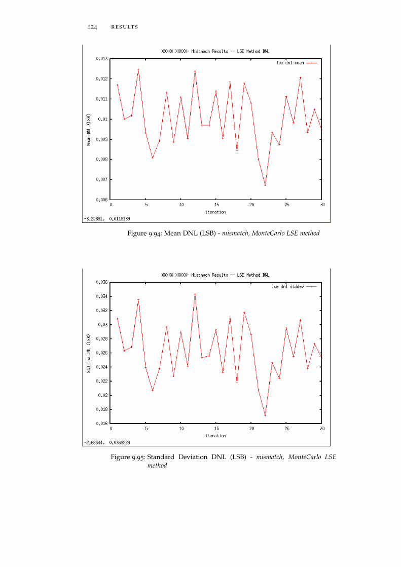
124 results
Figure 9.94: Mean DNL (LSB) - mismatch, MonteCarlo LSE method
Figure 9.95: Standard Deviation DNL (LSB) - mismatch, MonteCarlo LSEmethod
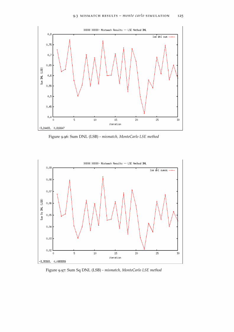
9.3 mismatch results – monte carlo simulation 125
Figure 9.96: Sum DNL (LSB) - mismatch, MonteCarlo LSE method
Figure 9.97: Sum Sq DNL (LSB) - mismatch, MonteCarlo LSE method
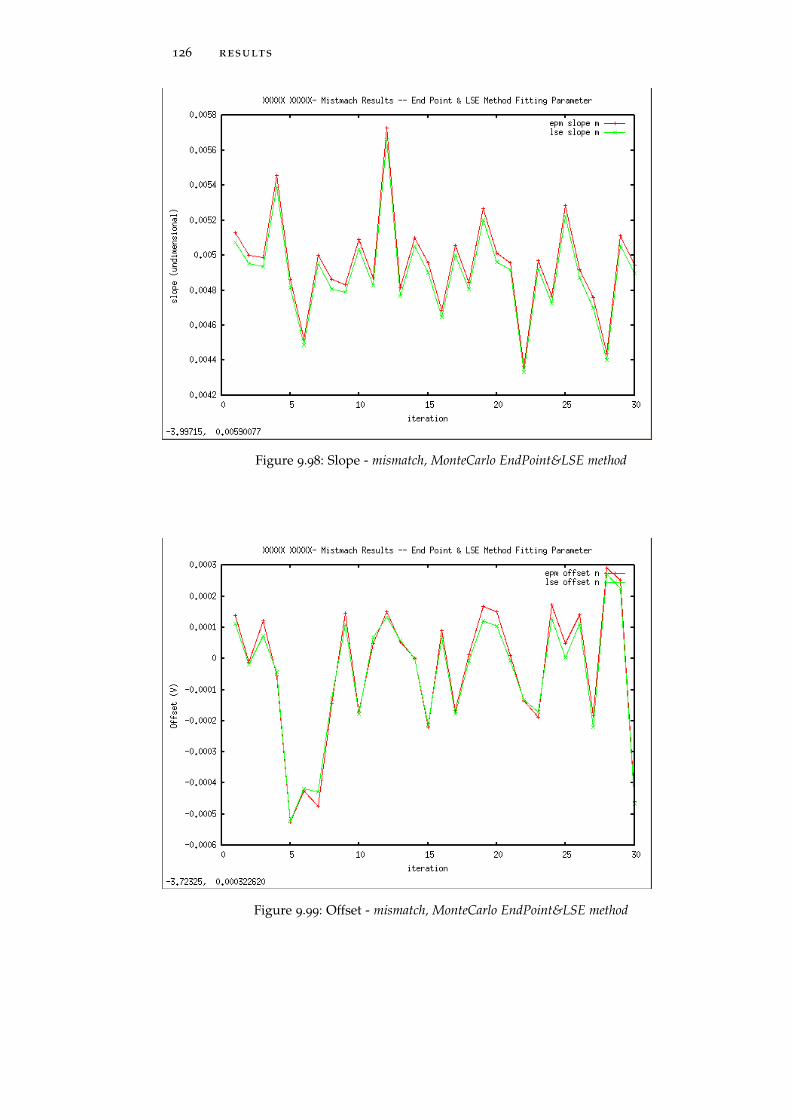
126 results
Figure 9.98: Slope - mismatch, MonteCarlo EndPoint&LSE method
Figure 9.99: Offset - mismatch, MonteCarlo EndPoint&LSE method
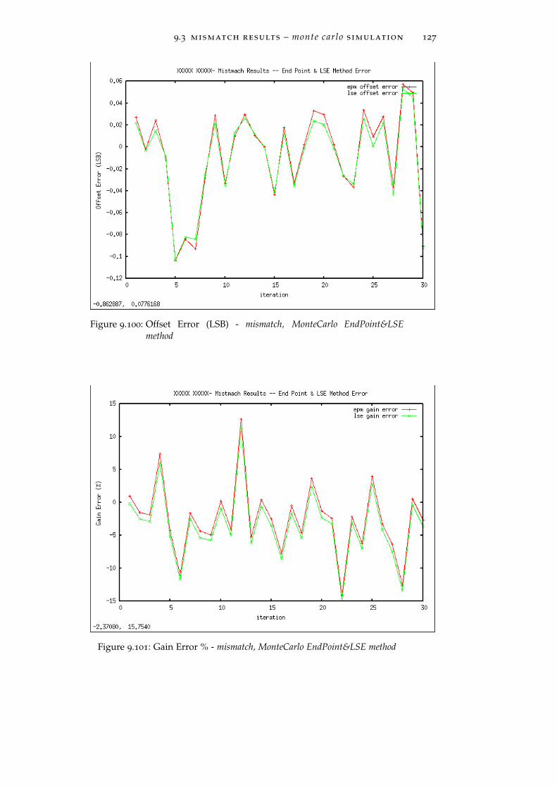
9.3 mismatch results – monte carlo simulation 127
Figure 9.100: Offset Error (LSB) - mismatch, MonteCarlo EndPoint&LSEmethod
Figure 9.101: Gain Error % - mismatch, MonteCarlo EndPoint&LSE method
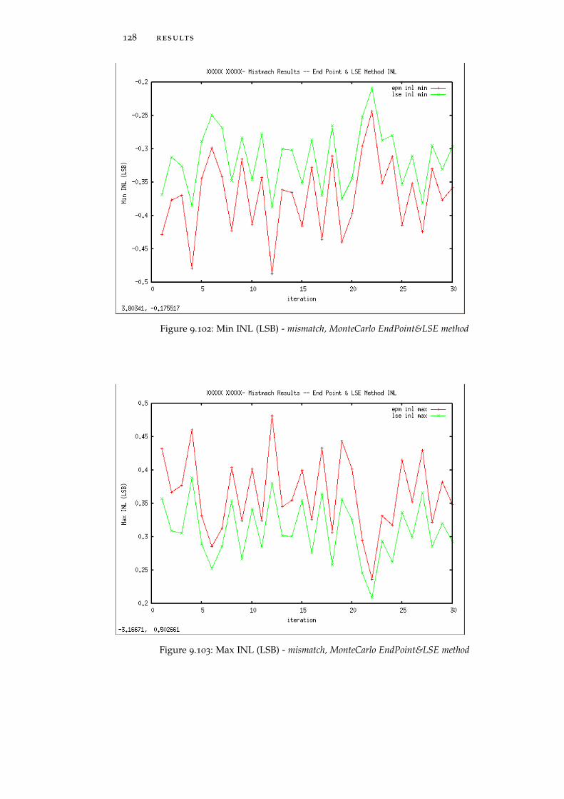
128 results
Figure 9.102: Min INL (LSB) - mismatch, MonteCarlo EndPoint&LSE method
Figure 9.103: Max INL (LSB) - mismatch, MonteCarlo EndPoint&LSE method
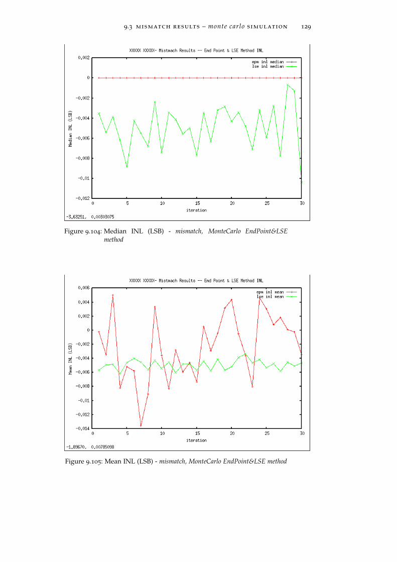
9.3 mismatch results – monte carlo simulation 129
Figure 9.104: Median INL (LSB) - mismatch, MonteCarlo EndPoint&LSEmethod
Figure 9.105: Mean INL (LSB) - mismatch, MonteCarlo EndPoint&LSE method
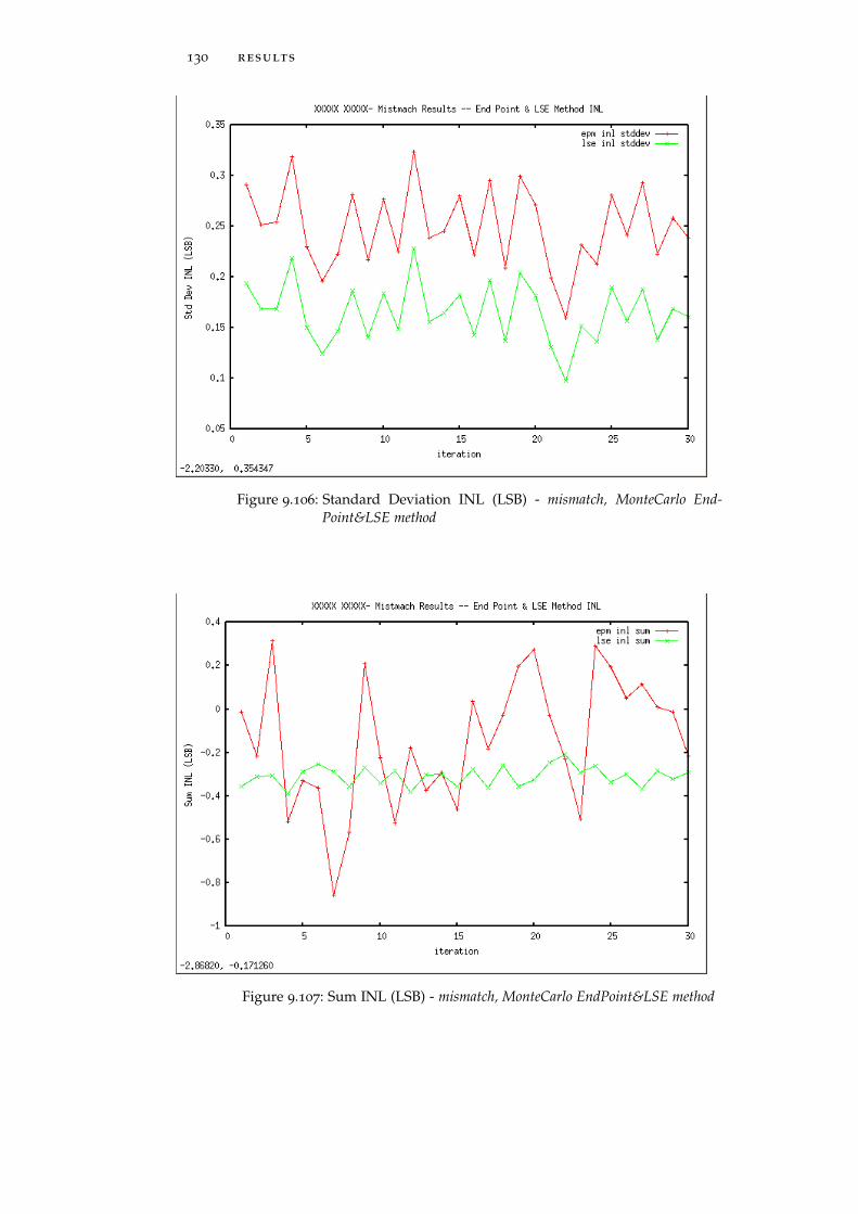
130 results
Figure 9.106: Standard Deviation INL (LSB) - mismatch, MonteCarlo End-Point&LSE method
Figure 9.107: Sum INL (LSB) - mismatch, MonteCarlo EndPoint&LSE method
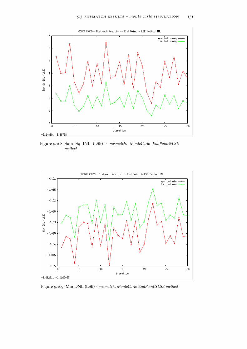
9.3 mismatch results – monte carlo simulation 131
Figure 9.108: Sum Sq INL (LSB) - mismatch, MonteCarlo EndPoint&LSEmethod
Figure 9.109: Min DNL (LSB) - mismatch, MonteCarlo EndPoint&LSE method
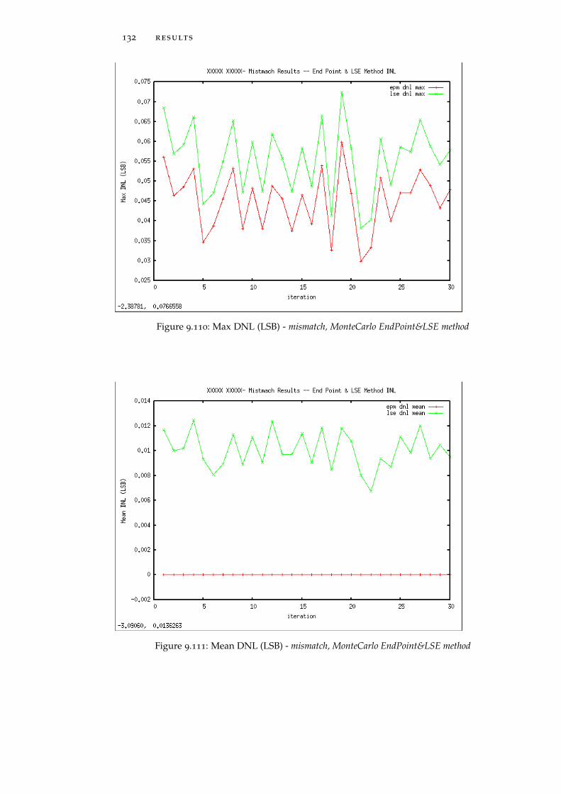
132 results
Figure 9.110: Max DNL (LSB) - mismatch, MonteCarlo EndPoint&LSE method
Figure 9.111: Mean DNL (LSB) - mismatch, MonteCarlo EndPoint&LSE method

9.3 mismatch results – monte carlo simulation 133
Figure 9.112: Standard Deviation DNL (LSB) - mismatch, MonteCarlo End-Point&LSE method
Figure 9.113: Sum DNL (LSB) - mismatch, MonteCarlo EndPoint&LSE method
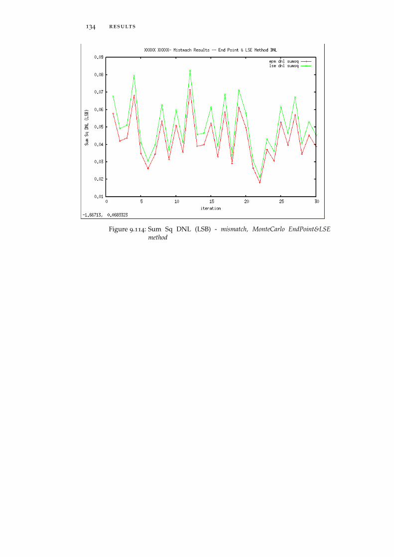
134 results
Figure 9.114: Sum Sq DNL (LSB) - mismatch, MonteCarlo EndPoint&LSEmethod

9.4 conclusions 135
9.4 conclusions
The aim of this work was the optimization of a threshold configurableregenerative comparator for ultra-low power battery-less applicationsand the analysis of the effect that this power reduction has over non-linearity in a 6-bit TC-ADC.
The power optimized comparator cuts down on 77% the powerconsumption and improves by a 20% the maximum sampling rate fora constant FS specification of ±160mV. The higher energy efficiencycauses improved linearity (about 50% for offset, gain, DNL and INL er-rors) for perfectly matched devices, while it exhibits higher sensitivityto dynamic random errors (21% worse INL for mismatched devices).Gain error is significatively improved even in the presence of randomerrors.
Future work has to be done by using the higher predictability ofINL errors obtained for the power optimized comparator in order tosimplify the calibrating networks.


Part IV
A P P E N D I X

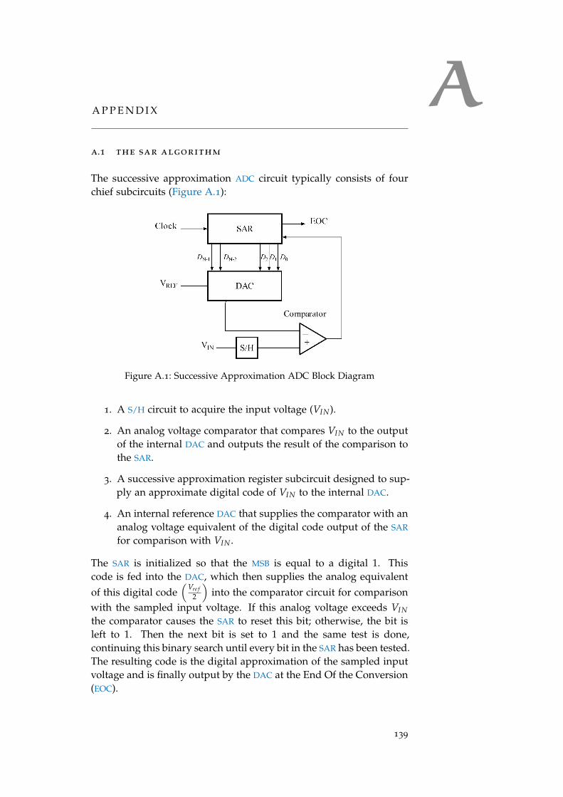
AA P P E N D I X
a.1 the sar algorithm
The successive approximation ADC circuit typically consists of fourchief subcircuits (Figure A.1):
Figure A.1: Successive Approximation ADC Block Diagram
1. A S/H circuit to acquire the input voltage (VIN).
2. An analog voltage comparator that compares VIN to the outputof the internal DAC and outputs the result of the comparison tothe SAR.
3. A successive approximation register subcircuit designed to sup-ply an approximate digital code of VIN to the internal DAC.
4. An internal reference DAC that supplies the comparator with ananalog voltage equivalent of the digital code output of the SAR
for comparison with VIN .
The SAR is initialized so that the MSB is equal to a digital 1. Thiscode is fed into the DAC, which then supplies the analog equivalentof this digital code
(Vre f
2
)into the comparator circuit for comparison
with the sampled input voltage. If this analog voltage exceeds VIN
the comparator causes the SAR to reset this bit; otherwise, the bit isleft to 1. Then the next bit is set to 1 and the same test is done,continuing this binary search until every bit in the SAR has been tested.The resulting code is the digital approximation of the sampled inputvoltage and is finally output by the DAC at the End Of the Conversion(EOC).
139
140 appendix
Mathematically, assume Vin = x Vre f , so that x in [−1, 1] is the nor-malized input voltage. The objective is to approximately digitize x toan accuracy of 1
2n . The algorithm proceeds as follows:
1. Initial approximation x0 = 0.
2. ith approximation xi = xi−1 − s(xi−1−x)2i .
where s (x) is the signum-function sgn(x) (+1 for x ≥ 0, −1 for x < 0).It follows, by mathematical induction, that |xn− x| ≤ 1
2n . [47]As shown in the above algorithm, a SAR ADC requires:
a. An input voltage source VIN .
b. A reference voltage source Vre f to normalize the input.
c. A DAC to convert the ith approximation xi to a voltage.
d. A Comparator to perform the function s (xi − x) by comparingthe DAC’s voltage with the input voltage.
e. A Register to store the output of the comparator and applyxi−1 − s(xi−1−x)
2i .
a.2 nyquist sampling condition
The Nyquist–Shannon sampling theorem, after Harry Nyquist andClaude Shannon, in the literature more commonly referred to as theNyquist sampling condition, is a fundamental result in the field ofinformation theory.
Shannon’s version of the theorem states:
If a function x(t) contains no frequencies higher thanB Hz, it is completely determined by giving its ordinatesat a series of points spaced 1
2B s apart.
In other words, a bandlimited function can be perfectly reconstructedfrom an infinite sequence of samples if the bandlimit B is no greaterthan 1
2 the sampling rate (samples per second). The theorem alsoleads to a formula for reconstruction of the original function from itssamples. When the bandlimit is too high (or there is no bandlimit),the reconstruction exhibits imperfections known as aliasing. The Pois-son summation formula provides a graphic understanding of aliasingand an alternative derivation of the theorem, using the perspective ofthe function’s Fourier transform. In practice of course, infinite se-quences, perfect sampling, and perfect interpolation are all replacedby approximations that deviate from the mathematical ideal of per-fect reconstruction. Moreover, the theorem is a sufficient, but notnecessary, condition.
A.3 nyquist frequency 141
To formalize the statements above, let X( f ) be the Fourier trans-form of the bandlimited function x(t):
X( f )de f=
∞∫−∞
x(t)e−i2π f tdt (A.1)
and assume thatX( f ) = 0, ∀ | f | > B
When x(t) is uniformly sampled at intervals of T seconds, the result-ing sequence is denoted by x(nT), for all integer values of n, and thesample-rate (samples per second) is:
fsde f=
1T
A sufficient condition to reconstruct x(t) from its samples is fs > 2B,or equivalently B < fs
2 . The two thresholds, 2B and fs2 , are respec-
tively called the Nyquist rate and Nyquist frequency. And they areattributes of x(t) and of the sampling equipment respectively. Thecondition described by these inequalities is called the Nyquist condi-tion [48].
a.3 nyquist frequency
The Nyquist frequency is half the sampling frequency of a discretesignal processing system [49, 50]. It is sometimes known as the fold-ing frequency of a sampling system [51].
When the continuous function to be sampled contains no frequen-cies equal or higher than the Nyquist frequency, all the aliases causedby sampling occur above the Nyquist frequency. The term aliasingusually refers to the case where some original frequency componentshave aliases below Nyquist. That often causes distortion when a con-tinuous function is subsequently reconstructed from samples.[52]
a.4 corner of process
In semiconductor manufacturing, a process corner is an example ofa Design-of-Experiments (DoE) technique that refers to a variation offabrication parameters used in applying an integrated circuit designto a semiconductor wafer. Process corners represent the extremes ofthese parameter variations within which a circuit that has been etchedonto the wafer must correctly function (Figure A.2 ):
• Slow corner. Everything goes wrong, that is all process varia-tions deviate towards a device with reduced currents.
• Fast corner. Everything is better than planned, that is allprocess variations deviate towards a device with increased cur-rents.

142 appendix
PMOS Speed
NMOS Speed
Typical
Fast N Fast P
Slow N Slow P Fast N Slow P
Slow N Fast Pσ
Figure A.2: Process corners in PMOS/NMOS fabrication parameters
• Cross corners. One device type has increased, the other typereduced currents.
A circuit running on devices fabricated at these process corners mayrun slower or faster than specified and at lower or higher tempera-tures and voltages, but if the circuit does not function at all at any ofthese process extremes the design is considered to have inadequatedesign margin [53].
In Very-Large-Scale-Integrated (VLSI) circuit microprocessor designand semiconductor fabrication, a process corner represents a three orsix sigma variation from nominal doping concentrations (and otherparameters) in transistors on a silicon wafer. This variation can causesignificant changes in the duty cycle and slew rate of digital signals,and it can sometimes result in catastrophic failure of the entire system.Variation may occur for many reasons, such as minor changes in thehumidity or temperature changes in the clean-room when wafers aretransported, or due to the position of the die relative to the center ofthe wafer [54].
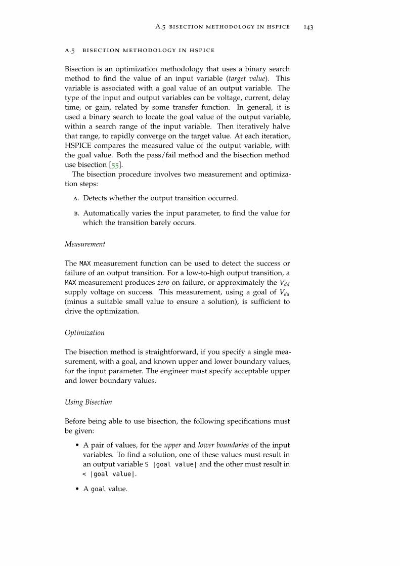
A.5 bisection methodology in hspice 143
a.5 bisection methodology in hspice
Bisection is an optimization methodology that uses a binary searchmethod to find the value of an input variable (target value). Thisvariable is associated with a goal value of an output variable. Thetype of the input and output variables can be voltage, current, delaytime, or gain, related by some transfer function. In general, it isused a binary search to locate the goal value of the output variable,within a search range of the input variable. Then iteratively halvethat range, to rapidly converge on the target value. At each iteration,HSPICE compares the measured value of the output variable, withthe goal value. Both the pass/fail method and the bisection methoduse bisection [55].
The bisection procedure involves two measurement and optimiza-tion steps:
a. Detects whether the output transition occurred.
b. Automatically varies the input parameter, to find the value forwhich the transition barely occurs.
Measurement
The MAX measurement function can be used to detect the success orfailure of an output transition. For a low-to-high output transition, aMAX measurement produces zero on failure, or approximately the Vddsupply voltage on success. This measurement, using a goal of Vdd(minus a suitable small value to ensure a solution), is sufficient todrive the optimization.
Optimization
The bisection method is straightforward, if you specify a single mea-surement, with a goal, and known upper and lower boundary values,for the input parameter. The engineer must specify acceptable upperand lower boundary values.
Using Bisection
Before being able to use bisection, the following specifications mustbe given:
• A pair of values, for the upper and lower boundaries of the inputvariables. To find a solution, one of these values must result inan output variable S |goal value| and the other must result in< |goal value|.
• A goal value.
144 appendix
Figure A.3: Bisection Example for Three Iterations
• Error tolerance value. The bisection process stops when the dif-ference between successive test values is minor or equal to theerror tolerance. If the other criteria are also met, see below.
• Related variables. A monotonic transfer function to relate vari-ables has to be used. A steadily-progressing time (increase ordecrease) results in a single occurrence of the goal value at thetarget input variable value.
HSPICE includes the error tolerance in a relation, used as a process-termination criterion.
Figure A.3 shows an example of the binary search process, whichthe bisection algorithm uses. This example is the pass/fail type, andfor example it is appropriate for a setup-time analysis that tests forthe presence of an output transition. In this case:

A.5 bisection methodology in hspice 145
1. A long setup time TS(= T2 − T1) results in a VOUT transition (apass).
2. A too-short setup time (where the latch has not stabilized theinput data, before the clock transition) results in a fail.
3. For example, it is possible to define a pass time value as anysetup time, TS, that produces a VOUT output equal to the mini-mum High logic output level (2.7V), which is the goal value.
4. The target value is a setup time that just produces the VOUTvalue of 2.7V. Finding the exact value is impractical, if notimpossible, so specify an error tolerance, to calculate a solutionarbitrarily close to the target value.
5. The bisection algorithm performs tests for each specified bound-ary value, to determine the direction in which to pursue the tar-get value, after the first bisection. In this example, the upperboundary has a pass value, and the lower boundary has a failvalue.
6. To start the binary search, specify the lower and upper bound-aries. The program tests the point midway between the lowerand upper boundaries.
a) If the initial value passes the test, the target value must beless than the tested value (in this example). The bisectionalgorithm moves the upper search limit to the value that itjust tested.
b) If the test fails, the target value must be greater than thetested value. Bisection moves the lower limit to the valuethat it just tested.
7. The algorithm tests a value midway between the new limits.
8. The search continues in this manner, moving one limit or theother to the last midpoint, and testing the value midway be-tween the new limits.
9. The process stops when the difference between the latest twotest values is less than or equal to the specified error tolerance.To normalize this value, there is to multiply by the initial bound-ary range.
Command Syntax
The following syntax is used for bisection:
.MODEL <OptModelName> OPT METHOD=BISECTION ... �
146 appendix
or
.MODEL <OptModelName> OPT METHOD=PASSFAIL ... �OptModelName is the model to be used. The METHOD keyword indi-
cates which optimization method to use. The OPT keyword indicatesthat optimization is to be performed.
For bisection, the method can be one of the following:
• BISECTION. When the difference between the two latest test in-put values is within the error tolerance and the latest measuredvalue exceeds the goal, bisection has succeeded and then ends.This process reports the optimized parameter that correspondedto the test value that satisfies this error tolerance and this goal(passes).
• PASSFAIL. When the difference between the two latest test inputvalues is within the error tolerance and one of the values ≥ goal(passes) and the other fails, bisection has succeeded and thenends. The process reports the input parameter value associatedwith the “pass” measurement.
The parameters are passed in a normal optimization specification:
.PARAM <ParamName>=<OptParFun> (<Initial>, <Lower>, <Upper>) �In the BISECTION method, the measure results for <Lower> and
<Upper> limits of <ParamName> must be on opposite sides of the goalvalue in the .MEASURE statement. In the PASSFAIL method, the mea-sure must pass for one limit and fail for the other limit. The processignores the value of the <Initial> field. The error tolerance is a pa-rameter in the model being optimized. In both methods, bisectionalsearch is applied to only one parameter.
When the OPTLST option is set (.OPTION OPTLST=1), the process out-puts the following information for the BISECTION method:
bisec-opt iter = <num_iterations> xlo = <low_val> xhi = <high_val
>
x = <result_low_val> xnew = <result_high_val>
err = <error_tolerance> �The x is the old parameter value and xnew is the new parameter
value.When .OPTION OPTLST=1, the process outputs the following infor-
mation for the PASSFAIL method:
bisec-opt iter = <num_iterations> xlo = <low_val> xhi = <high_val
>
A.6 tcadc file code 147
x = <result_low_val> xnew = <result_high_val>
measfail = 1 �In this syntax, measfail = 0 for a test failure for the x value.
Performing Transient Analyses with Bisections
When performing transient analysis bisection with the .TRAN state-ment, use the following syntax:
.TRAN <TranStep> <TranTime> SWEEP OPTIMIZE=<OptParFun>
+ RESULTS=<MeasureNames> MODEL=<OptModelName> �When performing a transient analysis bisection with the .MEASURE
statement, use the following syntax:
.MEASURE TRAN <MeasureName> <MeasureClause> GOAL=<GoalValue> �a.6 tcadc file code
It is presented the Perl code for the tcadc file, actually the main filewhich contains all the preprocessing simulation commands, parame-ters, stimulus, netlist, measurements and probe points that have to berun.
Listing 1: tcadc
#!/usr/bin/perl
$inputstr = ’ s ’;$inputm = 1;
$dotest = 0;
$noiseprocess = 0;
if($#ARGV == 0){
$inputstr = $ARGV[0];
}
elsif($#ARGV == 1) {
$inputstr = $ARGV[0];
$inputm = $ARGV[1];
}
elsif($#ARGV == 2) {
$inputstr = $ARGV[0];
$inputm = $ARGV[1];
}
elsif($#ARGV == 3) {
$inputstr = $ARGV[0];
$inputsts = $ARGV[1];
$inputm = $ARGV[2];
}
else {
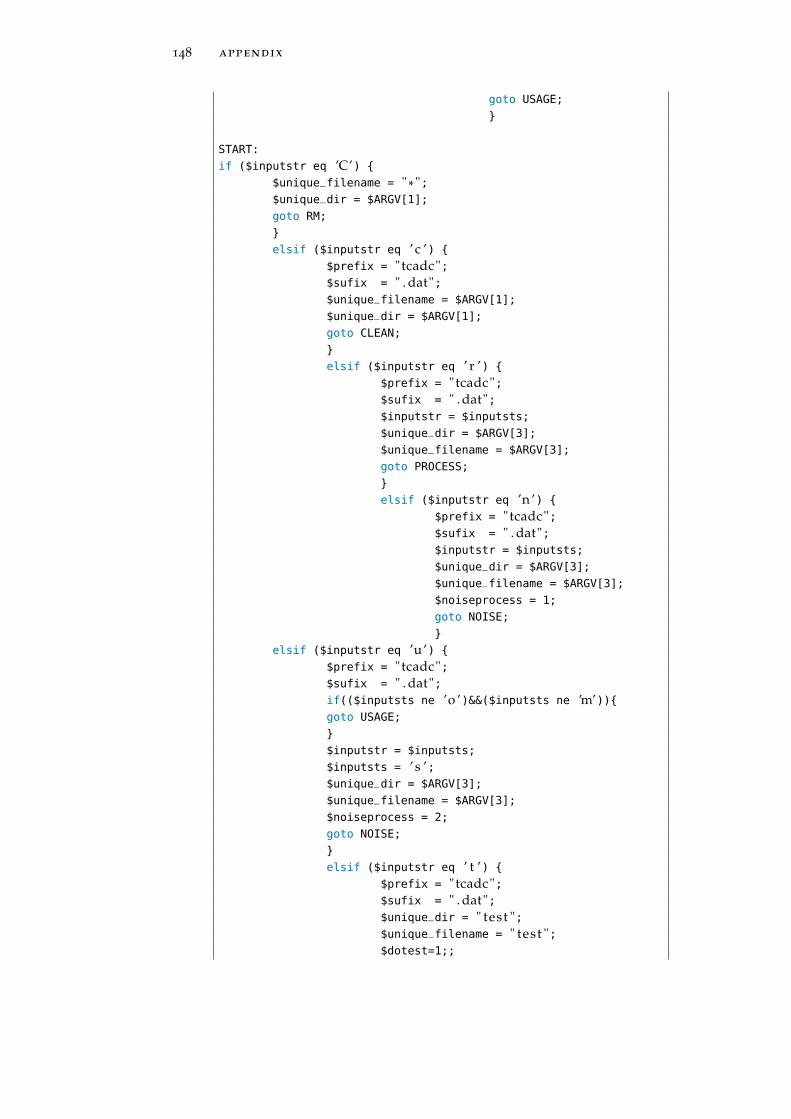
148 appendix
goto USAGE;
}
START:
if ($inputstr eq ’C’) {
$unique_filename = " * ";$unique_dir = $ARGV[1];
goto RM;
}
elsif ($inputstr eq ’ c ’) {
$prefix = " tcadc";$sufix = " . dat";$unique_filename = $ARGV[1];
$unique_dir = $ARGV[1];
goto CLEAN;
}
elsif ($inputstr eq ’ r ’) {
$prefix = " tcadc";$sufix = " . dat";$inputstr = $inputsts;
$unique_dir = $ARGV[3];
$unique_filename = $ARGV[3];
goto PROCESS;
}
elsif ($inputstr eq ’n ’) {
$prefix = " tcadc";$sufix = " . dat";$inputstr = $inputsts;
$unique_dir = $ARGV[3];
$unique_filename = $ARGV[3];
$noiseprocess = 1;
goto NOISE;
}
elsif ($inputstr eq ’u ’) {
$prefix = " tcadc";$sufix = " . dat";if(($inputsts ne ’o ’)&&($inputsts ne ’m’)){goto USAGE;
}
$inputstr = $inputsts;
$inputsts = ’ s ’;$unique_dir = $ARGV[3];
$unique_filename = $ARGV[3];
$noiseprocess = 2;
goto NOISE;
}
elsif ($inputstr eq ’ t ’) {
$prefix = " tcadc";$sufix = " . dat";$unique_dir = " test ";$unique_filename = " test ";$dotest=1;;

A.6 tcadc file code 149
goto MKDIR;
}
elsif ($inputstr eq ’x ’) {
$prefix = " tcadc";$sufix = " . dat";$inputstr = $inputsts;
$unique_dir = $ARGV[3];
$unique_filename = $ARGV[3];
goto RERUN;
}
elsif ((($inputstr eq ’m’)||($inputstr eq ’o ’)||($inputstr eq ’ s ’))&&($#ARGV == 2)){
$prefix = " tcadc";$sufix = " . dat";$unique_filename = $ARGV[2];
$unique_dir = $ARGV[2];
goto MKDIR;
}
elsif ((($inputstr eq ’m’)||($inputstr eq ’o ’)||($inputstr eq ’ s ’))&&($#ARGV == 1)){
$prefix = " tcadc";$sufix = " . dat";$unique_filename = $prefix . "_" .
get_timestamp();
$unique_dir = $unique_filename;
goto MKDIR;
}
NOISE:
$mkvth = " . ./ bin/mkvthsp ";$vthfile = $unique_dir . "/" . $prefix . $sufix . $inputstr .
$inputm . "−vth";$spfile = $unique_dir . "/" . $prefix . $sufix . $inputstr .
$inputm . "−vth−sp";$command = join " ", $mkvth, " ", $vthfile, " > ", $spfile;
print "\n";print " . . . processing command: $command\n";print "\n";system($command);
$command = join " ", " cat ", "pre−", $inputsts, "header . sp > ",$inputsts, "header . sp";
@args = ($command);
print "\n";print " . . . generating header f i l e : @args\n";print "\n";system(@args);
if(($inputsts eq ’m’)){$command = join " ", " printf \" monte=%d\\n\"", " ",
$inputm, " >> ", $inputsts, "header . sp";@args = ($command);
print "\n";print " . . . generating header f i l e : @args\n";
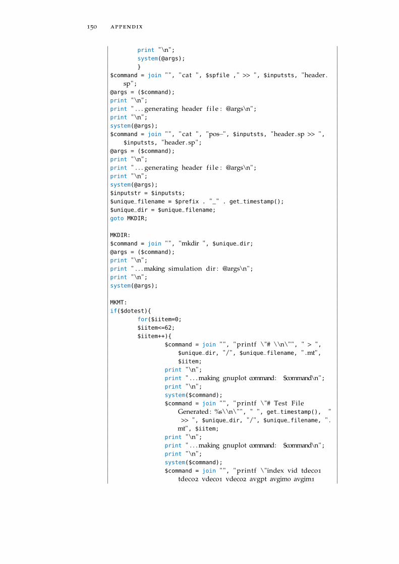
150 appendix
print "\n";system(@args);
}
$command = join " ", " cat ", $spfile ," >> ", $inputsts, "header .sp";
@args = ($command);
print "\n";print " . . . generating header f i l e : @args\n";print "\n";system(@args);
$command = join " ", " cat ", "pos−", $inputsts, "header . sp >> ",$inputsts, "header . sp";
@args = ($command);
print "\n";print " . . . generating header f i l e : @args\n";print "\n";system(@args);
$inputstr = $inputsts;
$unique_filename = $prefix . "_" . get_timestamp();
$unique_dir = $unique_filename;
goto MKDIR;
MKDIR:
$command = join " ", "mkdir ", $unique_dir;
@args = ($command);
print "\n";print " . . . making simulation dir : @args\n";print "\n";system(@args);
MKMT:
if($dotest){
for($iitem=0;
$iitem<=62;
$iitem++){
$command = join " ", " printf \"# \\n\"", " > ",$unique_dir, "/", $unique_filename, " .mt",$iitem;
print "\n";print " . . . making gnuplot command: $command\n";print "\n";system($command);
$command = join " ", " printf \"# Test FileGenerated : %s\\n\"", " ", get_timestamp(), ">> ", $unique_dir, "/", $unique_filename, " .
mt", $iitem;
print "\n";print " . . . making gnuplot command: $command\n";print "\n";system($command);
$command = join " ", " printf \"index vid tdeco1
tdeco2 vdeco1 vdeco2 avgpt avgim0 avgim1
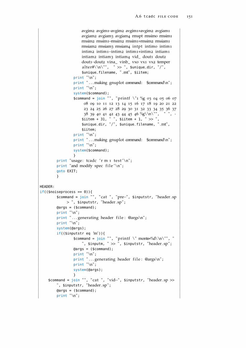
A.6 tcadc file code 151
avgim2 avgim1−avgim2 avgim1+avgim2 avgiam1
avgiam2 avgiam3 avgiam4 rmspt rmsim0 rmsim1
rmsim2 rmsim1−rmsim2 rmsim1+rmsim2 rmsiam1
rmsiam2 rmsiam3 rmsiam4 intpt intim0 intim1
intim2 intim1−intim2 intim1+intim2 intiam1
intiam2 intiam3 intiam4 vid_ dout1 dout2dout1−dout2 vina_ vinb_ vx0 vx1 vx2 temperalter#\\n\"", " >> ", $unique_dir, "/",$unique_filename, " .mt", $iitem;
print "\n";print " . . . making gnuplot command: $command\n";print "\n";system($command);
$command = join " ", " printf \"1 %g 03 04 05 06 07
08 09 10 11 12 13 14 15 16 17 18 19 20 21 22
23 24 25 26 27 28 29 30 31 32 33 34 35 36 37
38 39 40 41 42 43 44 45 46 %g\\n\"", " ", -
$iitem + 31, " ", $iitem + 1, " >> ",$unique_dir, "/", $unique_filename, " .mt",$iitem;
print "\n";print " . . . making gnuplot command: $command\n";print "\n";system($command);
}
print "usage : tcadc ’ r m 1 test ’\n";print "and modify spec f i l e ’\n";goto EXIT;
}
HEADER:
if(($noiseprocess == 0)){
$command = join " ", " cat ", "pre−", $inputstr, "header . sp> ", $inputstr, "header . sp";
@args = ($command);
print "\n";print " . . . generating header f i l e : @args\n";print "\n";system(@args);
if(($inputstr eq ’m’)){$command = join " ", " printf \" monte=%d\\n\"", "
", $inputm, " >> ", $inputstr, "header . sp";@args = ($command);
print "\n";print " . . . generating header f i l e : @args\n";print "\n";system(@args);
}
$command = join " ", " cat ", "vid−", $inputstr, "header . sp >>", $inputstr, "header . sp";@args = ($command);
print "\n";
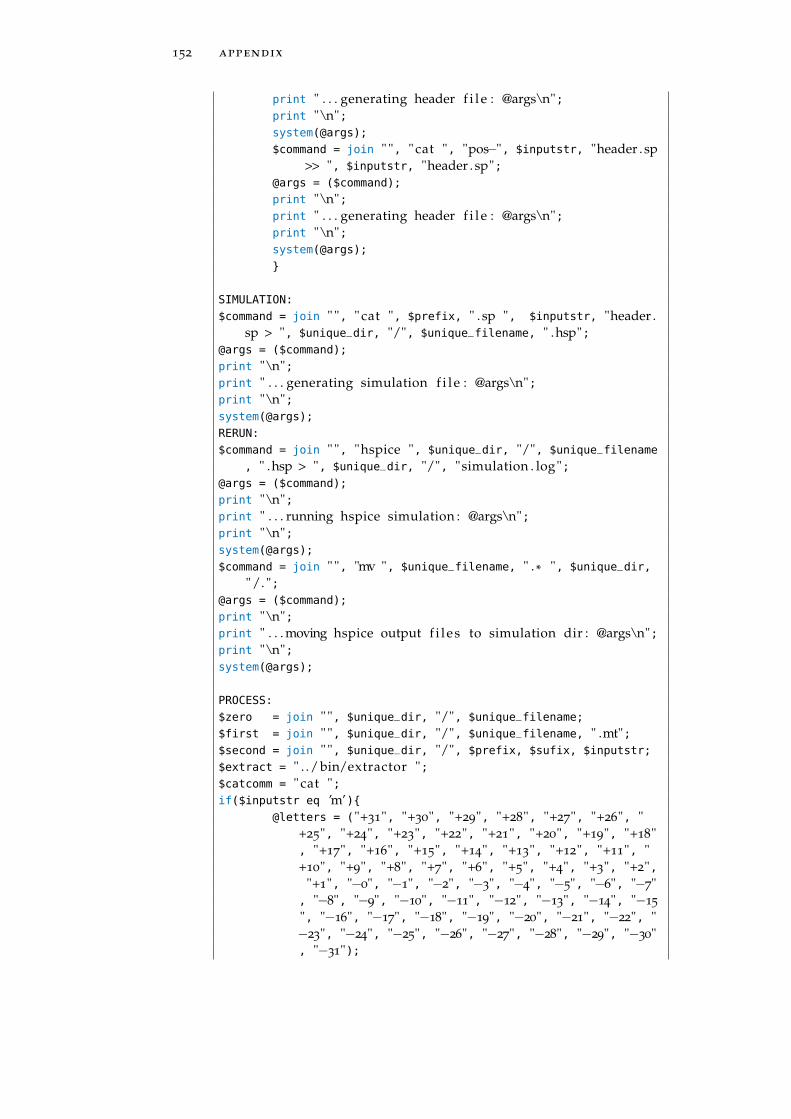
152 appendix
print " . . . generating header f i l e : @args\n";print "\n";system(@args);
$command = join " ", " cat ", "pos−", $inputstr, "header . sp>> ", $inputstr, "header . sp";
@args = ($command);
print "\n";print " . . . generating header f i l e : @args\n";print "\n";system(@args);
}
SIMULATION:
$command = join " ", " cat ", $prefix, " . sp ", $inputstr, "header .sp > ", $unique_dir, "/", $unique_filename, " .hsp";
@args = ($command);
print "\n";print " . . . generating simulation f i l e : @args\n";print "\n";system(@args);
RERUN:
$command = join " ", "hspice ", $unique_dir, "/", $unique_filename
, " .hsp > ", $unique_dir, "/", "simulation . log";@args = ($command);
print "\n";print " . . . running hspice simulation : @args\n";print "\n";system(@args);
$command = join " ", "mv ", $unique_filename, " . * ", $unique_dir,
"/. ";@args = ($command);
print "\n";print " . . . moving hspice output f i l es to simulation dir : @args\n";print "\n";system(@args);
PROCESS:
$zero = join " ", $unique_dir, "/", $unique_filename;
$first = join " ", $unique_dir, "/", $unique_filename, " .mt";$second = join " ", $unique_dir, "/", $prefix, $sufix, $inputstr;
$extract = " . ./ bin/extractor ";$catcomm = " cat ";if($inputstr eq ’m’){
@letters = ("+31", "+30", "+29", "+28", "+27", "+26", "+25", "+24", "+23", "+22", "+21", "+20", "+19", "+18", "+17", "+16", "+15", "+14", "+13", "+12", "+11", "+10", "+9", "+8", "+7", "+6", "+5", "+4", "+3", "+2",
"+1", "−0", "−1", "−2", "−3", "−4", "−5", "−6", "−7", "−8", "−9", "−10", "−11", "−12", "−13", "−14", "−15
", "−16", "−17", "−18", "−19", "−20", "−21", "−22", "−23", "−24", "−25", "−26", "−27", "−28", "−29", "−30", "−31");
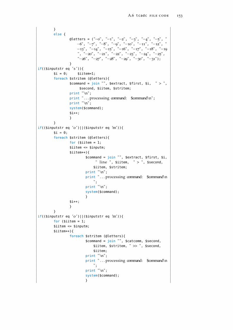
A.6 tcadc file code 153
}
else {
@letters = ("−0", "−1", "−2", "−3", "−4", "−5", "−6", "−7", "−8", "−9", "−10", "−11", "−12", "−13", "−14", "−15", "−16", "−17", "−18", "−19
", "−20", "−21", "−22", "−23", "−24", "−25","−26", "−27", "−28", "−29", "−30", "−31");
}
if(($inputstr eq ’ s ’)){$i = 0; $iitem=1;
foreach $stritem (@letters){
$command = join " ", $extract, $first, $i, " > ",$second, $iitem, $stritem;
print "\n";print " . . . processing command: $command\n";print "\n";system($command);
$i++;
}
}
if(($inputstr eq ’o ’)||($inputstr eq ’m’)){$i = 0;
foreach $stritem (@letters){
for ($iitem = 1;
$iitem <= $inputm;
$iitem++){
$command = join " ", $extract, $first, $i,
" line ", $iitem, " > ", $second,
$iitem, $stritem;
print "\n";print " . . . processing command: $command\n
";print "\n";system($command);
}
$i++;
}
}
if(($inputstr eq ’o ’)||($inputstr eq ’m’)){for ($iitem = 1;
$iitem <= $inputm;
$iitem++){
foreach $stritem (@letters){
$command = join " ", $catcomm, $second,
$iitem, $stritem, " >> ", $second,
$iitem;
print "\n";print " . . . processing command: $command\n
";print "\n";system($command);
}

154 appendix
if($inputstr eq ’o ’){$command = join " ", $catcomm, $second,
$iitem, "−0 ", $second, $iitem, "−31
> ", $second, $iitem, "−0", "−31";print "\n";print " . . . processing command: $command\n
";print "\n";system($command);
}
else {
$command = join " ", $catcomm,
$second, $iitem, "+31 ",$second, $iitem, "−31 > ",$second, $iitem, "+31", "−31";
print "\n";print " . . . processing command:
$command\n";print "\n";system($command);
}
}
}
if(($inputstr eq ’o ’)||($inputstr eq ’m’)) {
$j = 0;
foreach $stritem (@letters){
$j++;
if($j==1){
$stritem1 = $stritem;
}
elsif($j==2){
$stritem2 = $stritem;
for ($iitem = 1; $iitem
<= $inputm; $iitem++)
{
$command = join "", $extract,
$second,
$iitem,
$stritem1, "", $second,
$iitem,
$stritem2, "> ", $second,
$iitem,
$stritem1,
$stritem2;
print "\n";print " . . .
processing
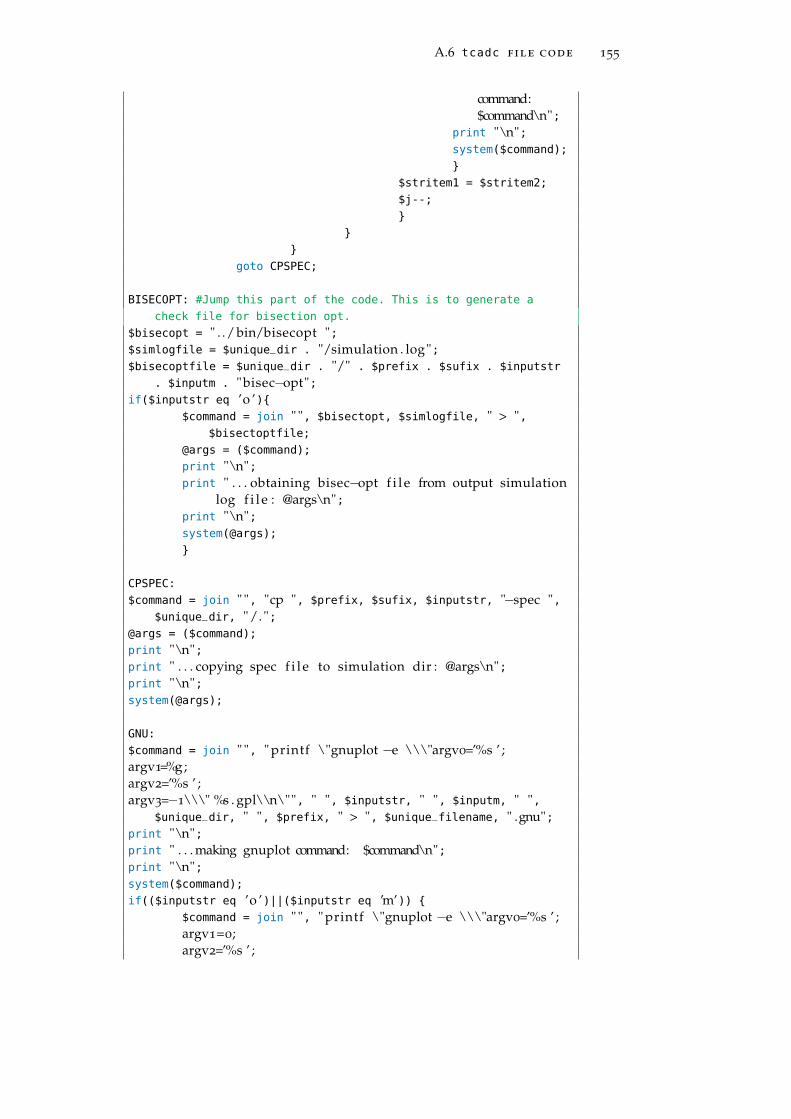
A.6 tcadc file code 155
command:$command\n";
print "\n";system($command);
}
$stritem1 = $stritem2;
$j--;
}
}
}
goto CPSPEC;
BISECOPT: #Jump this part of the code. This is to generate a
check file for bisection opt.
$bisecopt = " . ./ bin/bisecopt ";$simlogfile = $unique_dir . "/simulation . log";$bisecoptfile = $unique_dir . "/" . $prefix . $sufix . $inputstr
. $inputm . "bisec−opt";if($inputstr eq ’o ’){
$command = join " ", $bisectopt, $simlogfile, " > ",$bisectoptfile;
@args = ($command);
print "\n";print " . . . obtaining bisec−opt f i l e from output simulation
log f i l e : @args\n";print "\n";system(@args);
}
CPSPEC:
$command = join " ", "cp ", $prefix, $sufix, $inputstr, "−spec ",$unique_dir, "/. ";
@args = ($command);
print "\n";print " . . . copying spec f i l e to simulation dir : @args\n";print "\n";system(@args);
GNU:
$command = join " ", " printf \"gnuplot −e \\\"argv0=’%s ’ ;argv1=%g;argv2=’%s ’ ;argv3=−1\\\" %s . gpl\\n\"", " ", $inputstr, " ", $inputm, " ",
$unique_dir, " ", $prefix, " > ", $unique_filename, " .gnu";print "\n";print " . . . making gnuplot command: $command\n";print "\n";system($command);
if(($inputstr eq ’o ’)||($inputstr eq ’m’)) {
$command = join " ", " printf \"gnuplot −e \\\"argv0=’%s ’ ;argv1=0;argv2=’%s ’ ;
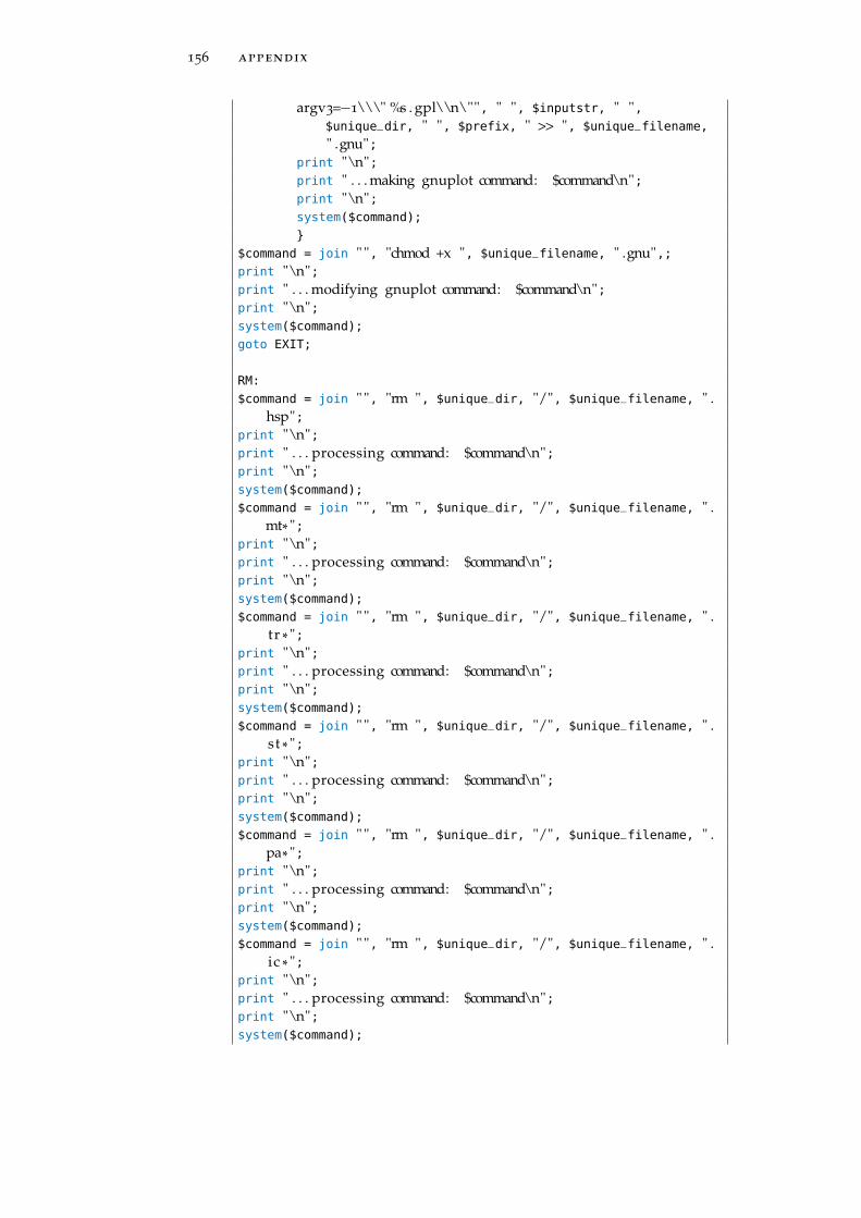
156 appendix
argv3=−1\\\" %s . gpl\\n\"", " ", $inputstr, " ",$unique_dir, " ", $prefix, " >> ", $unique_filename,
" .gnu";print "\n";print " . . . making gnuplot command: $command\n";print "\n";system($command);
}
$command = join " ", "chmod +x ", $unique_filename, " .gnu",;print "\n";print " . . . modifying gnuplot command: $command\n";print "\n";system($command);
goto EXIT;
RM:
$command = join " ", "rm ", $unique_dir, "/", $unique_filename, " .hsp";
print "\n";print " . . . processing command: $command\n";print "\n";system($command);
$command = join " ", "rm ", $unique_dir, "/", $unique_filename, " .mt* ";
print "\n";print " . . . processing command: $command\n";print "\n";system($command);
$command = join " ", "rm ", $unique_dir, "/", $unique_filename, " .tr * ";
print "\n";print " . . . processing command: $command\n";print "\n";system($command);
$command = join " ", "rm ", $unique_dir, "/", $unique_filename, " .st * ";
print "\n";print " . . . processing command: $command\n";print "\n";system($command);
$command = join " ", "rm ", $unique_dir, "/", $unique_filename, " .pa* ";
print "\n";print " . . . processing command: $command\n";print "\n";system($command);
$command = join " ", "rm ", $unique_dir, "/", $unique_filename, " .ic * ";
print "\n";print " . . . processing command: $command\n";print "\n";system($command);

A.6 tcadc file code 157
CLEAN:
$command = join " ", "rm ", $unique_dir, "/", $prefix, $sufix, " * ";
print "\n";print " . . . processing command: $command\n";print "\n";system($command);
$command = join " ", "rm *tmp";print "\n";print " . . . processing command: $command\n";print "\n";system($command);
$command = join " ", "rm *.*~ ";print "\n";print " . . . processing command: $command\n";print "\n";system($command);
$command = join " ", "rm *~";print "\n";print " . . . processing command: $command\n";print "\n";system($command);
EXIT: print "\n";print " . . . That ’ s a l l folks\n";print "\n";exit;
USAGE:
print "usage : tcadc ’ t ’|{ ’ s ’| ’o’| ’m’ index { tag } , index=1 ,2 ,3 . . . }| ’x ’| ’ r ’| ’u’| ’n ’ ’ s ’| ’o’| ’m’ { . . . } tag\n";
print "C: do a hard clean ;c : do a soft clean ;\n";print " t : test ;s : scan mode;o : bisection opt . ;m: montecarlo + bisection opt ;\n";print "x : rerun simulation (do a soft clean f i r s t ) ;r : pos−process simulation (do a soft clean f i r s t ) ;\n";print "n: do noise analysis\n";print "u: from ’o’| ’m’ to scan mode with noise analysis ;\n";print " tag : directory tag ;\n";exit;
sub get_timestamp {
@abbr = qw( Jan Feb Mar Apr May Jun Jul Aug Sep Oct Nov
Dec );
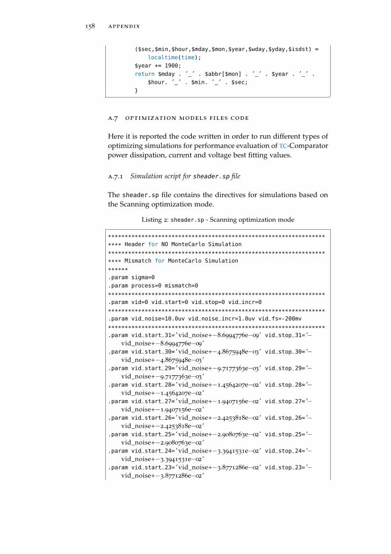
158 appendix
($sec,$min,$hour,$mday,$mon,$year,$wday,$yday,$isdst) =
localtime(time);
$year += 1900;
return $mday . ’_ ’ . $abbr[$mon] . ’_ ’ . $year . ’_ ’ .
$hour. ’_ ’ . $min. ’_ ’ . $sec;
} �a.7 optimization models files code
Here it is reported the code written in order to run different types ofoptimizing simulations for performance evaluation of TC-Comparatorpower dissipation, current and voltage best fitting values.
a.7.1 Simulation script for sheader.sp file
The sheader.sp file contains the directives for simulations based onthe Scanning optimization mode.
Listing 2: sheader.sp - Scanning optimization mode
*****************************************************************
**** Header for NO MonteCarlo Simulation
*****************************************************************
**** Mismatch for MonteCarlo Simulation
******.param sigma=0
.param process=0 mismatch=0
*****************************************************************.param vid=0 vid_start=0 vid_stop=0 vid_incr=0
*****************************************************************.param vid_noise=10.0uv vid_noise_incr=1.0uv vid_fs=-200mv
*****************************************************************.param vid_start_31= ’vid_noise+−8.6994776e−09’ vid_stop_31= ’−
vid_noise+−8.6994776e−09’.param vid_start_30= ’vid_noise+−4.8675948e−03’ vid_stop_30= ’−
vid_noise+−4.8675948e−03’.param vid_start_29= ’vid_noise+−9.7177363e−03’ vid_stop_29= ’−
vid_noise+−9.7177363e−03’.param vid_start_28= ’vid_noise+−1.4564207e−02’ vid_stop_28= ’−
vid_noise+−1.4564207e−02’.param vid_start_27= ’vid_noise+−1.9407156e−02’ vid_stop_27= ’−
vid_noise+−1.9407156e−02’.param vid_start_26= ’vid_noise+−2.4253818e−02’ vid_stop_26= ’−
vid_noise+−2.4253818e−02’.param vid_start_25= ’vid_noise+−2.9080763e−02’ vid_stop_25= ’−
vid_noise+−2.9080763e−02’.param vid_start_24= ’vid_noise+−3.3941531e−02’ vid_stop_24= ’−
vid_noise+−3.3941531e−02’.param vid_start_23= ’vid_noise+−3.8771286e−02’ vid_stop_23= ’−
vid_noise+−3.8771286e−02’

A.7 optimization models files code 159
.param vid_start_22= ’vid_noise+−4.3659324e−02’ vid_stop_22= ’−vid_noise+−4.3659324e−02’
.param vid_start_21= ’vid_noise+−4.8545729e−02’ vid_stop_21= ’−vid_noise+−4.8545729e−02’
.param vid_start_20= ’vid_noise+−5.3428821e−02’ vid_stop_20= ’−vid_noise+−5.3428821e−02’
.param vid_start_19= ’vid_noise+−5.8357190e−02’ vid_stop_19= ’−vid_noise+−5.8357190e−02’
.param vid_start_18= ’vid_noise+−6.3295966e−02’ vid_stop_18= ’−vid_noise+−6.3295966e−02’
.param vid_start_17= ’vid_noise+−6.8252648e−02’ vid_stop_17= ’−vid_noise+−6.8252648e−02’
.param vid_start_16= ’vid_noise+−7.3236715e−02’ vid_stop_16= ’−vid_noise+−7.3236715e−02’
.param vid_start_15= ’vid_noise+−7.8241682e−02’ vid_stop_15= ’−vid_noise+−7.8241682e−02’
.param vid_start_14= ’vid_noise+−8.3272059e−02’ vid_stop_14= ’−vid_noise+−8.3272059e−02’
.param vid_start_13= ’vid_noise+−8.8300299e−02’ vid_stop_13= ’−vid_noise+−8.8300299e−02’
.param vid_start_12= ’vid_noise+−9.3413144e−02’ vid_stop_12= ’−vid_noise+−9.3413144e−02’
.param vid_start_11= ’vid_noise+−9.8463285e−02’ vid_stop_11= ’−vid_noise+−9.8463285e−02’
.param vid_start_10= ’vid_noise+−1.0359673e−01’ vid_stop_10= ’−vid_noise+−1.0359673e−01’
.param vid_start_9= ’vid_noise+−1.0874526e−01’ vid_stop_9= ’−vid_noise+−1.0874526e−01’
.param vid_start_8= ’vid_noise+−1.1384806e−01’ vid_stop_8= ’−vid_noise+−1.1384806e−01’
.param vid_start_7= ’vid_noise+−1.1900904e−01’ vid_stop_7= ’−vid_noise+−1.1900904e−01’
.param vid_start_6= ’vid_noise+−1.2420357e−01’ vid_stop_6= ’−vid_noise+−1.2420357e−01’
.param vid_start_5= ’vid_noise+−1.2932084e−01’ vid_stop_5= ’−vid_noise+−1.2932084e−01’
.param vid_start_4= ’vid_noise+−1.3459414e−01’ vid_stop_4= ’−vid_noise+−1.3459414e−01’
.param vid_start_3= ’vid_noise+−1.3976896e−01’ vid_stop_3= ’−vid_noise+−1.3976896e−01’
.param vid_start_2= ’vid_noise+−1.4495092e−01’ vid_stop_2= ’−vid_noise+−1.4495092e−01’
.param vid_start_1= ’vid_noise+−1.5013130e−01’ vid_stop_1= ’−vid_noise+−1.5013130e−01’
.param vid_start_0= ’vid_noise+−1.5523863e−01’ vid_stop_0= ’−vid_noise+−1.5523863e−01’
*****************************************************************.title ’00000 00000 − Scan for Threshold Voltage Determination ’******.param vtca4=0 vtca3=0 vtca2=0 vtca1=0 vtca0=0
.param vtcb4=0 vtcb3=0 vtcb2=0 vtcb1=0 vtcb0=0
******

160 appendix
.param vid_start=vid_start_31 vid_stop=vid_stop_31 vid_incr=
vid_noise_incr
******.tran 0.1p ’2*T+2n’ sweep vid vid_start vid_stop vid_incr
*****************************************************************
*****************************************************************.alter .title ’00001 00000 − Scan for Threshold Voltage
Determination ’.param vtca4=0 vtca3=0 vtca2=0 vtca1=0 vtca0=1
.param vid_start=vid_start_30 vid_stop=vid_stop_30 vid_incr=
vid_noise_incr
*****************************************************************
*****************************************************************.alter .title ’000010 00000 − Scan for Threshold Voltage
Determination ’.param vtca4=0 vtca3=0 vtca2=0 vtca1=1 vtca0=0
.param vid_start=vid_start_29 vid_stop=vid_stop_29 vid_incr=
vid_noise_incr
*****************************************************************
*****************************************************************.alter .title ’000011 00000 − Scan for Threshold Voltage
Determination ’.param vtca4=0 vtca3=0 vtca2=0 vtca1=1 vtca0=1
.param vid_start=vid_start_28 vid_stop=vid_stop_28 vid_incr=
vid_noise_incr
*****************************************************************
*****************************************************************.alter .title ’000100 00000 − Scan for Threshold Voltage
Determination ’.param vtca4=0 vtca3=0 vtca2=1 vtca1=0 vtca0=0
.param vid_start=vid_start_27 vid_stop=vid_stop_27 vid_incr=
vid_noise_incr
*****************************************************************
*****************************************************************.alter .title ’000101 00000 − Scan for Threshold Voltage
Determination ’.param vtca4=0 vtca3=0 vtca2=1 vtca1=0 vtca0=1
.param vid_start=vid_start_26 vid_stop=vid_stop_26 vid_incr=
vid_noise_incr
*****************************************************************
*****************************************************************.alter .title ’000110 00000 − Scan for Threshold Voltage
Determination ’.param vtca4=0 vtca3=0 vtca2=1 vtca1=1 vtca0=0
.param vid_start=vid_start_25 vid_stop=vid_stop_25 vid_incr=
vid_noise_incr
*****************************************************************
*****************************************************************.alter .title ’000111 00000 − Scan for Threshold Voltage
Determination ’.param vtca4=0 vtca3=0 vtca2=1 vtca1=1 vtca0=1

A.7 optimization models files code 161
.param vid_start=vid_start_24 vid_stop=vid_stop_24 vid_incr=
vid_noise_incr
*****************************************************************
*****************************************************************.alter .title ’001000 00000 − Scan for Threshold Voltage
Determination ’.param vtca4=0 vtca3=1 vtca2=0 vtca1=0 vtca0=0
.param vid_start=vid_start_23 vid_stop=vid_stop_23 vid_incr=
vid_noise_incr
*****************************************************************.alter .title ’001001 00000 − Scan for Threshold Voltage
Determination ’.param vtca4=0 vtca3=1 vtca2=0 vtca1=0 vtca0=1
.param vid_start=vid_start_22 vid_stop=vid_stop_22 vid_incr=
vid_noise_incr
*****************************************************************.alter .title ’001010 00000 − Scan for Threshold Voltage
Determination ’.param vtca4=0 vtca3=1 vtca2=0 vtca1=1 vtca0=0
.param vid_start=vid_start_21 vid_stop=vid_stop_21 vid_incr=
vid_noise_incr
*****************************************************************.alter .title ’001011 00000 − Scan for Threshold Voltage
Determination ’.param vtca4=0 vtca3=1 vtca2=0 vtca1=1 vtca0=1
.param vid_start=vid_start_20 vid_stop=vid_stop_20 vid_incr=
vid_noise_incr
*****************************************************************.alter .title ’001100 00000 − Scan for Threshold Voltage
Determination ’.param vtca4=0 vtca3=1 vtca2=1 vtca1=0 vtca0=0
.param vid_start=vid_start_19 vid_stop=vid_stop_19 vid_incr=
vid_noise_incr
*****************************************************************.alter .title ’001101 00000 − Scan for Threshold Voltage
Determination ’.param vtca4=0 vtca3=1 vtca2=1 vtca1=0 vtca0=1
.param vid_start=vid_start_18 vid_stop=vid_stop_18 vid_incr=
vid_noise_incr
*****************************************************************.alter .title ’001110 00000 − Scan for Threshold Voltage
Determination ’.param vtca4=0 vtca3=1 vtca2=1 vtca1=1 vtca0=0
.param vid_start=vid_start_17 vid_stop=vid_stop_17 vid_incr=
vid_noise_incr
*****************************************************************.alter .title ’001111 00000 − Scan for Threshold Voltage
Determination ’.param vtca4=0 vtca3=1 vtca2=1 vtca1=1 vtca0=1
.param vid_start=vid_start_16 vid_stop=vid_stop_16 vid_incr=
vid_noise_incr
*****************************************************************
162 appendix
.alter .title ’10000 00000 − Scan for Threshold VoltageDetermination ’
.param vtca4=1 vtca3=0 vtca2=0 vtca1=0 vtca0=0
.param vid_start=vid_start_15 vid_stop=vid_stop_15 vid_incr=
vid_noise_incr
*****************************************************************.alter .title ’10001 00000 − Scan for Threshold Voltage
Determination ’.param vtca4=1 vtca3=0 vtca2=0 vtca1=0 vtca0=1
.param vid_start=vid_start_14 vid_stop=vid_stop_14 vid_incr=
vid_noise_incr
*****************************************************************.alter .title ’10010 00000 − Scan for Threshold Voltage
Determination ’.param vtca4=1 vtca3=0 vtca2=0 vtca1=1 vtca0=0
.param vid_start=vid_start_13 vid_stop=vid_stop_13 vid_incr=
vid_noise_incr
*****************************************************************.alter .title ’10011 00000 − Scan for Threshold Voltage
Determination ’.param vtca4=1 vtca3=0 vtca2=0 vtca1=1 vtca0=1
.param vid_start=vid_start_12 vid_stop=vid_stop_12 vid_incr=
vid_noise_incr
*****************************************************************.alter .title ’10100 00000 − Scan for Threshold Voltage
Determination ’.param vtca4=1 vtca3=0 vtca2=1 vtca1=0 vtca0=0
.param vid_start=vid_start_11 vid_stop=vid_stop_11 vid_incr=
vid_noise_incr
*****************************************************************.alter .title ’10101 00000 − Scan for Threshold Voltage
Determination ’.param vtca4=1 vtca3=0 vtca2=1 vtca1=0 vtca0=1
.param vid_start=vid_start_10 vid_stop=vid_stop_10 vid_incr=
vid_noise_incr
*****************************************************************.alter .title ’10110 00000 − Scan for Threshold Voltage
Determination ’.param vtca4=1 vtca3=0 vtca2=1 vtca1=1 vtca0=0
.param vid_start=vid_start_9 vid_stop=vid_stop_9 vid_incr=
vid_noise_incr
*****************************************************************.alter .title ’10111 00000 − Scan for Threshold Voltage
Determination ’.param vtca4=1 vtca3=0 vtca2=1 vtca1=1 vtca0=1
.param vid_start=vid_start_8 vid_stop=vid_stop_8 vid_incr=
vid_noise_incr
*****************************************************************.alter .title ’11000 00000 − Scan for Threshold Voltage
Determination ’.param vtca4=1 vtca3=1 vtca2=0 vtca1=0 vtca0=0

A.7 optimization models files code 163
.param vid_start=vid_start_7 vid_stop=vid_stop_7 vid_incr=
vid_noise_incr
*****************************************************************.alter .title ’11001 00000 − Scan for Threshold Voltage
Determination ’.param vtca4=1 vtca3=1 vtca2=0 vtca1=0 vtca0=1
.param vid_start=vid_start_6 vid_stop=vid_stop_6 vid_incr=
vid_noise_incr
*****************************************************************.alter .title ’11010 00000 − Scan for Threshold Voltage
Determination ’.param vtca4=1 vtca3=1 vtca2=0 vtca1=1 vtca0=0
.param vid_start=vid_start_5 vid_stop=vid_stop_5 vid_incr=
vid_noise_incr
*****************************************************************.alter .title ’11011 00000 − Scan for Threshold Voltage
Determination ’.param vtca4=1 vtca3=1 vtca2=0 vtca1=1 vtca0=1
.param vid_start=vid_start_4 vid_stop=vid_stop_4 vid_incr=
vid_noise_incr
*****************************************************************.alter .title ’11100 00000 − Scan for Threshold Voltage
Determination ’.param vtca4=1 vtca3=1 vtca2=1 vtca1=0 vtca0=0
.param vid_start=vid_start_3 vid_stop=vid_stop_3 vid_incr=
vid_noise_incr
*****************************************************************.alter .title ’11101 00000 − Scan for Threshold Voltage
Determination ’.param vtca4=1 vtca3=1 vtca2=1 vtca1=0 vtca0=1
.param vid_start=vid_start_2 vid_stop=vid_stop_2 vid_incr=
vid_noise_incr
*****************************************************************.alter .title ’11110 00000 − Scan for Threshold Voltage
Determination ’.param vtca4=1 vtca3=1 vtca2=1 vtca1=1 vtca0=0
.param vid_start=vid_start_1 vid_stop=vid_stop_1 vid_incr=
vid_noise_incr
*****************************************************************.alter .title ’11111 00000 − Scan for Threshold Voltage
Determination ’.param vtca4=1 vtca3=1 vtca2=1 vtca1=1 vtca0=1
.param vid_start=vid_start_0 vid_stop=vid_stop_0 vid_incr=
vid_noise_incr
*****************************************************************
*****************************************************************.end �
164 appendix
a.7.2 Simulation script for oheader.sp file
The oheader.sp file contains the directives for simulations made byusing the Bisection optimization mode.
Listing 3: oheader.sp - Bisection optimization mode
*****************************************************************
**** Header for NO MonteCarlo Simulation
*****************************************************************
**** Mismatch for MonteCarlo Simulation
******.param sigma=0 .param process=0 mismatch=0
*****************************************************************.param vid=0 vid_start=0 vid_stop=0 vid_incr=0
*****************************************************************.param vid_noise=1.0mv vid_noise_incr=1.0mv
*****************************************************************.param vid_start_31= ’vid_noise+−3.05e−06’ vid_stop_31= ’−vid_noise
+−3.05e−06’.param vid_start_30= ’vid_noise+−4.87e−03’ vid_stop_30= ’−vid_noise
+−4.87e−03’.param vid_start_29= ’vid_noise+−9.73e−03’ vid_stop_29= ’−vid_noise
+−9.73e−03’.param vid_start_28= ’vid_noise+−1.46e−02’ vid_stop_28= ’−vid_noise
+−1.46e−02’.param vid_start_27= ’vid_noise+−1.94e−02’ vid_stop_27= ’−vid_noise
+−1.94e−02’.param vid_start_26= ’vid_noise+−2.42e−02’ vid_stop_26= ’−vid_noise
+−2.42e−02’.param vid_start_25= ’vid_noise+−2.91e−02’ vid_stop_25= ’−vid_noise
+−2.91e−02’.param vid_start_24= ’vid_noise+−3.39e−02’ vid_stop_24= ’−vid_noise
+−3.39e−02’.param vid_start_23= ’vid_noise+−3.88e−02’ vid_stop_23= ’−vid_noise
+−3.88e−02’.param vid_start_22= ’vid_noise+−4.37e−02’ vid_stop_22= ’−vid_noise
+−4.37e−02’.param vid_start_21= ’vid_noise+−4.85e−02’ vid_stop_21= ’−vid_noise
+−4.85e−02’.param vid_start_20= ’vid_noise+−5.34e−02’ vid_stop_20= ’−vid_noise
+−5.34e−02’.param vid_start_19= ’vid_noise+−5.84e−02’ vid_stop_19= ’−vid_noise
+−5.84e−02’.param vid_start_18= ’vid_noise+−6.33e−02’ vid_stop_18= ’−vid_noise
+−6.33e−02’.param vid_start_17= ’vid_noise+−6.83e−02’ vid_stop_17= ’−vid_noise
+−6.83e−02’.param vid_start_16= ’vid_noise+−7.32e−02’ vid_stop_16= ’−vid_noise
+−7.32e−02’.param vid_start_15= ’vid_noise+−7.82e−02’ vid_stop_15= ’−vid_noise
+−7.82e−02’
A.7 optimization models files code 165
.param vid_start_14= ’vid_noise+−8.33e−02’ vid_stop_14= ’−vid_noise+−8.33e−02’
.param vid_start_13= ’vid_noise+−8.83e−02’ vid_stop_13= ’−vid_noise+−8.83e−02’
.param vid_start_12= ’vid_noise+−9.34e−02’ vid_stop_12= ’−vid_noise+−9.34e−02’
.param vid_start_11= ’vid_noise+−9.85e−02’ vid_stop_11= ’−vid_noise+−9.85e−02’
.param vid_start_10= ’vid_noise+−1.04e−01’ vid_stop_10= ’−vid_noise+−1.04e−01’
.param vid_start_9= ’vid_noise+−1.09e−01’ vid_stop_9= ’−vid_noise+−1.09e−01’
.param vid_start_8= ’vid_noise+−1.14e−01’ vid_stop_8= ’−vid_noise+−1.14e−01’
.param vid_start_7= ’vid_noise+−1.19e−01’ vid_stop_7= ’−vid_noise+−1.19e−01’
.param vid_start_6= ’vid_noise+−1.24e−01’ vid_stop_6= ’−vid_noise+−1.24e−01’
.param vid_start_5= ’vid_noise+−1.29e−01’ vid_stop_5= ’−vid_noise+−1.29e−01’
.param vid_start_4= ’vid_noise+−1.34e−01’ vid_stop_4= ’−vid_noise+−1.34e−01’
.param vid_start_3= ’vid_noise+−1.40e−01’ vid_stop_3= ’−vid_noise+−1.40e−01’
.param vid_start_2= ’vid_noise+−1.45e−01’ vid_stop_2= ’−vid_noise+−1.45e−01’
.param vid_start_1= ’vid_noise+−1.50e−01’ vid_stop_1= ’−vid_noise+−1.50e−01’
.param vid_start_0= ’vid_noise+−1.55e−01’ vid_stop_0= ’−vid_noise+−1.55e−01’
*****************************************************************.title ’00000 00000 − Scan for Threshold Voltage Determination ’******.param vtca4=0 vtca3=0 vtca2=0 vtca1=0 vtca0=0
.param vtcb4=0 vtcb3=0 vtcb2=0 vtcb1=0 vtcb0=0
******.param vid_start=vid_start_31 vid_stop=vid_stop_31 vid_incr=
vid_noise_incr
******.param vid=optadc(vid_start,vid_start,vid_stop)
******.tran 0.1p ’2*T+2n’ sweep optimize=optadc results=dout1-dout2
model=opt3
*****************************************************************
*****************************************************************.alter .title ’00001 00000 − Scan for Threshold Voltage
Determination ’.param vtca4=0 vtca3=0 vtca2=0 vtca1=0 vtca0=1
.param vid_start=vid_start_30 vid_stop=vid_stop_30 vid_incr=
vid_noise_incr
*****************************************************************
*****************************************************************
166 appendix
.alter .title ’000010 00000 − Scan for Threshold VoltageDetermination ’
.param vtca4=0 vtca3=0 vtca2=0 vtca1=1 vtca0=0
.param vid_start=vid_start_29 vid_stop=vid_stop_29 vid_incr=
vid_noise_incr
*****************************************************************
*****************************************************************.alter .title ’000011 00000 − Scan for Threshold Voltage
Determination ’.param vtca4=0 vtca3=0 vtca2=0 vtca1=1 vtca0=1
.param vid_start=vid_start_28 vid_stop=vid_stop_28 vid_incr=
vid_noise_incr
*****************************************************************
*****************************************************************.alter .title ’000100 00000 − Scan for Threshold Voltage
Determination ’.param vtca4=0 vtca3=0 vtca2=1 vtca1=0 vtca0=0
.param vid_start=vid_start_27 vid_stop=vid_stop_27 vid_incr=
vid_noise_incr
*****************************************************************
*****************************************************************.alter .title ’000101 00000 − Scan for Threshold Voltage
Determination ’.param vtca4=0 vtca3=0 vtca2=1 vtca1=0 vtca0=1
.param vid_start=vid_start_26 vid_stop=vid_stop_26 vid_incr=
vid_noise_incr
*****************************************************************
*****************************************************************.alter .title ’000110 00000 − Scan for Threshold Voltage
Determination ’.param vtca4=0 vtca3=0 vtca2=1 vtca1=1 vtca0=0
.param vid_start=vid_start_25 vid_stop=vid_stop_25 vid_incr=
vid_noise_incr
*****************************************************************
*****************************************************************.alter .title ’000111 00000 − Scan for Threshold Voltage
Determination ’.param vtca4=0 vtca3=0 vtca2=1 vtca1=1 vtca0=1
.param vid_start=vid_start_24 vid_stop=vid_stop_24 vid_incr=
vid_noise_incr
*****************************************************************
*****************************************************************.alter .title ’001000 00000 − Scan for Threshold Voltage
Determination ’.param vtca4=0 vtca3=1 vtca2=0 vtca1=0 vtca0=0
.param vid_start=vid_start_23 vid_stop=vid_stop_23 vid_incr=
vid_noise_incr
*****************************************************************.alter .title ’001001 00000 − Scan for Threshold Voltage
Determination ’.param vtca4=0 vtca3=1 vtca2=0 vtca1=0 vtca0=1
A.7 optimization models files code 167
.param vid_start=vid_start_22 vid_stop=vid_stop_22 vid_incr=
vid_noise_incr
*****************************************************************.alter .title ’001010 00000 − Scan for Threshold Voltage
Determination ’.param vtca4=0 vtca3=1 vtca2=0 vtca1=1 vtca0=0
.param vid_start=vid_start_21 vid_stop=vid_stop_21 vid_incr=
vid_noise_incr
*****************************************************************.alter .title ’001011 00000 − Scan for Threshold Voltage
Determination ’.param vtca4=0 vtca3=1 vtca2=0 vtca1=1 vtca0=1
.param vid_start=vid_start_20 vid_stop=vid_stop_20 vid_incr=
vid_noise_incr
*****************************************************************.alter .title ’001100 00000 − Scan for Threshold Voltage
Determination ’.param vtca4=0 vtca3=1 vtca2=1 vtca1=0 vtca0=0
.param vid_start=vid_start_19 vid_stop=vid_stop_19 vid_incr=
vid_noise_incr
*****************************************************************.alter .title ’001101 00000 − Scan for Threshold Voltage
Determination ’.param vtca4=0 vtca3=1 vtca2=1 vtca1=0 vtca0=1
.param vid_start=vid_start_18 vid_stop=vid_stop_18 vid_incr=
vid_noise_incr
*****************************************************************.alter .title ’001110 00000 − Scan for Threshold Voltage
Determination ’.param vtca4=0 vtca3=1 vtca2=1 vtca1=1 vtca0=0
.param vid_start=vid_start_17 vid_stop=vid_stop_17 vid_incr=
vid_noise_incr
*****************************************************************.alter .title ’001111 00000 − Scan for Threshold Voltage
Determination ’.param vtca4=0 vtca3=1 vtca2=1 vtca1=1 vtca0=1
.param vid_start=vid_start_16 vid_stop=vid_stop_16 vid_incr=
vid_noise_incr
*****************************************************************.alter .title ’10000 00000 − Scan for Threshold Voltage
Determination ’.param vtca4=1 vtca3=0 vtca2=0 vtca1=0 vtca0=0
.param vid_start=vid_start_15 vid_stop=vid_stop_15 vid_incr=
vid_noise_incr
*****************************************************************.alter .title ’10001 00000 − Scan for Threshold Voltage
Determination ’.param vtca4=1 vtca3=0 vtca2=0 vtca1=0 vtca0=1
.param vid_start=vid_start_14 vid_stop=vid_stop_14 vid_incr=
vid_noise_incr
*****************************************************************
168 appendix
.alter .title ’10010 00000 − Scan for Threshold VoltageDetermination ’
.param vtca4=1 vtca3=0 vtca2=0 vtca1=1 vtca0=0
.param vid_start=vid_start_13 vid_stop=vid_stop_13 vid_incr=
vid_noise_incr
*****************************************************************.alter .title ’10011 00000 − Scan for Threshold Voltage
Determination ’.param vtca4=1 vtca3=0 vtca2=0 vtca1=1 vtca0=1
.param vid_start=vid_start_12 vid_stop=vid_stop_12 vid_incr=
vid_noise_incr
*****************************************************************.alter .title ’10100 00000 − Scan for Threshold Voltage
Determination ’.param vtca4=1 vtca3=0 vtca2=1 vtca1=0 vtca0=0
.param vid_start=vid_start_11 vid_stop=vid_stop_11 vid_incr=
vid_noise_incr
*****************************************************************.alter .title ’10101 00000 − Scan for Threshold Voltage
Determination ’.param vtca4=1 vtca3=0 vtca2=1 vtca1=0 vtca0=1
.param vid_start=vid_start_10 vid_stop=vid_stop_10 vid_incr=
vid_noise_incr
*****************************************************************.alter .title ’10110 00000 − Scan for Threshold Voltage
Determination ’.param vtca4=1 vtca3=0 vtca2=1 vtca1=1 vtca0=0
.param vid_start=vid_start_9 vid_stop=vid_stop_9 vid_incr=
vid_noise_incr
*****************************************************************.alter .title ’10111 00000 − Scan for Threshold Voltage
Determination ’.param vtca4=1 vtca3=0 vtca2=1 vtca1=1 vtca0=1
.param vid_start=vid_start_8 vid_stop=vid_stop_8 vid_incr=
vid_noise_incr
*****************************************************************.alter .title ’11000 00000 − Scan for Threshold Voltage
Determination ’.param vtca4=1 vtca3=1 vtca2=0 vtca1=0 vtca0=0
.param vid_start=vid_start_7 vid_stop=vid_stop_7 vid_incr=
vid_noise_incr
*****************************************************************.alter .title ’11001 00000 − Scan for Threshold Voltage
Determination ’.param vtca4=1 vtca3=1 vtca2=0 vtca1=0 vtca0=1
.param vid_start=vid_start_6 vid_stop=vid_stop_6 vid_incr=
vid_noise_incr
*****************************************************************.alter .title ’11010 00000 − Scan for Threshold Voltage
Determination ’.param vtca4=1 vtca3=1 vtca2=0 vtca1=1 vtca0=0
A.7 optimization models files code 169
.param vid_start=vid_start_5 vid_stop=vid_stop_5 vid_incr=
vid_noise_incr
*****************************************************************.alter .title ’11011 00000 − Scan for Threshold Voltage
Determination ’.param vtca4=1 vtca3=1 vtca2=0 vtca1=1 vtca0=1
.param vid_start=vid_start_4 vid_stop=vid_stop_4 vid_incr=
vid_noise_incr
*****************************************************************.alter .title ’11100 00000 − Scan for Threshold Voltage
Determination ’.param vtca4=1 vtca3=1 vtca2=1 vtca1=0 vtca0=0
.param vid_start=vid_start_3 vid_stop=vid_stop_3 vid_incr=
vid_noise_incr
*****************************************************************.alter .title ’11101 00000 − Scan for Threshold Voltage
Determination ’.param vtca4=1 vtca3=1 vtca2=1 vtca1=0 vtca0=1
.param vid_start=vid_start_2 vid_stop=vid_stop_2 vid_incr=
vid_noise_incr
*****************************************************************.alter .title ’11110 00000 − Scan for Threshold Voltage
Determination ’.param vtca4=1 vtca3=1 vtca2=1 vtca1=1 vtca0=0
.param vid_start=vid_start_1 vid_stop=vid_stop_1 vid_incr=
vid_noise_incr
*****************************************************************.alter .title ’11111 00000 − Scan for Threshold Voltage
Determination ’.param vtca4=1 vtca3=1 vtca2=1 vtca1=1 vtca0=1
.param vid_start=vid_start_0 vid_stop=vid_stop_0 vid_incr=
vid_noise_incr
*****************************************************************
*****************************************************************.end �a.7.3 Simulation script for mheader file
The mheader.sp file contains the directives for mismatch analysis ledthrough Monte Carlo simulation technique.
Listing 4: mheader.sp - Monte Carlo optimization mode
*****************************************************************
**** Header for MonteCarlo Simulation
*****************************************************************
**** Mismatch for MonteCarlo Simulation
******.param sigma=3 .param process=0 mismatch=1
*****************************************************************
****** Analysis conditions
170 appendix
******.param vid_noise=0.0mv vid_noise_incr=1.0mv
*****************************************************************.param vid=-100mv vid_start=+1000.0mv vid_stop=-1000.0mv vid_incr
=-0.1mv
******.param vid=optadc(vid_start,vid_start,vid_stop)
******.tran 0.1p ’2*T+2n’ sweep optimize=optadc results=dout1-dout2
model=opt3 monte=30
*****************************************************************.param vid_noise=0.0mv vid_noise_incr=1.0mv vid_fs=200mv
*****************************************************************.param vid_start_62= ’vid_noise+vid_fs ’ vid_stop_62= ’−vid_noise−
vid_fs ’.param vid_start_61= ’vid_noise+vid_fs ’ vid_stop_61= ’−vid_noise−
vid_fs ’.param vid_start_60= ’vid_noise+vid_fs ’ vid_stop_60= ’−vid_noise−
vid_fs ’.param vid_start_59= ’vid_noise+vid_fs ’ vid_stop_59= ’−vid_noise−
vid_fs ’.param vid_start_58= ’vid_noise+vid_fs ’ vid_stop_58= ’−vid_noise−
vid_fs ’.param vid_start_57= ’vid_noise+vid_fs ’ vid_stop_57= ’−vid_noise−
vid_fs ’.param vid_start_56= ’vid_noise+vid_fs ’ vid_stop_56= ’−vid_noise−
vid_fs ’.param vid_start_55= ’vid_noise+vid_fs ’ vid_stop_55= ’−vid_noise−
vid_fs ’.param vid_start_54= ’vid_noise+vid_fs ’ vid_stop_54= ’−vid_noise−
vid_fs ’.param vid_start_53= ’vid_noise+vid_fs ’ vid_stop_53= ’−vid_noise−
vid_fs ’.param vid_start_52= ’vid_noise+vid_fs ’ vid_stop_52= ’−vid_noise−
vid_fs ’.param vid_start_51= ’vid_noise+vid_fs ’ vid_stop_51= ’−vid_noise−
vid_fs ’.param vid_start_50= ’vid_noise+vid_fs ’ vid_stop_50= ’−vid_noise−
vid_fs ’.param vid_start_49= ’vid_noise+vid_fs ’ vid_stop_49= ’−vid_noise−
vid_fs ’.param vid_start_48= ’vid_noise+vid_fs ’ vid_stop_48= ’−vid_noise−
vid_fs ’.param vid_start_47= ’vid_noise+vid_fs ’ vid_stop_47= ’−vid_noise−
vid_fs ’.param vid_start_46= ’vid_noise+vid_fs ’ vid_stop_46= ’−vid_noise−
vid_fs ’.param vid_start_45= ’vid_noise+vid_fs ’ vid_stop_45= ’−vid_noise−
vid_fs ’.param vid_start_44= ’vid_noise+vid_fs ’ vid_stop_44= ’−vid_noise−
vid_fs ’

A.7 optimization models files code 171
.param vid_start_43= ’vid_noise+vid_fs ’ vid_stop_43= ’−vid_noise−vid_fs ’
.param vid_start_42= ’vid_noise+vid_fs ’ vid_stop_42= ’−vid_noise−vid_fs ’
.param vid_start_41= ’vid_noise+vid_fs ’ vid_stop_41= ’−vid_noise−vid_fs ’
.param vid_start_40= ’vid_noise+vid_fs ’ vid_stop_40= ’−vid_noise−vid_fs ’
.param vid_start_39= ’vid_noise+vid_fs ’ vid_stop_39= ’−vid_noise−vid_fs ’
.param vid_start_38= ’vid_noise+vid_fs ’ vid_stop_38= ’−vid_noise−vid_fs ’
.param vid_start_37= ’vid_noise+vid_fs ’ vid_stop_37= ’−vid_noise−vid_fs ’
.param vid_start_36= ’vid_noise+vid_fs ’ vid_stop_36= ’−vid_noise−vid_fs ’
.param vid_start_35= ’vid_noise+vid_fs ’ vid_stop_35= ’−vid_noise−vid_fs ’
.param vid_start_34= ’vid_noise+vid_fs ’ vid_stop_34= ’−vid_noise−vid_fs ’
.param vid_start_33= ’vid_noise+vid_fs ’ vid_stop_33= ’−vid_noise−vid_fs ’
.param vid_start_32= ’vid_noise+vid_fs ’ vid_stop_32= ’−vid_noise−vid_fs ’
*****************************************************************.param vid_start_31= ’vid_noise+vid_fs ’ vid_stop_31= ’−vid_noise−
vid_fs ’*****************************************************************.param vid_start_30= ’vid_noise+vid_fs ’ vid_stop_30= ’−vid_noise−
vid_fs ’.param vid_start_29= ’vid_noise+vid_fs ’ vid_stop_29= ’−vid_noise−
vid_fs ’.param vid_start_28= ’vid_noise+vid_fs ’ vid_stop_28= ’−vid_noise−
vid_fs ’.param vid_start_27= ’vid_noise+vid_fs ’ vid_stop_27= ’−vid_noise−
vid_fs ’.param vid_start_26= ’vid_noise+vid_fs ’ vid_stop_26= ’−vid_noise−
vid_fs ’.param vid_start_25= ’vid_noise+vid_fs ’ vid_stop_25= ’−vid_noise−
vid_fs ’.param vid_start_24= ’vid_noise+vid_fs ’ vid_stop_24= ’−vid_noise−
vid_fs ’.param vid_start_23= ’vid_noise+vid_fs ’ vid_stop_23= ’−vid_noise−
vid_fs ’.param vid_start_22= ’vid_noise+vid_fs ’ vid_stop_22= ’−vid_noise−
vid_fs ’.param vid_start_21= ’vid_noise+vid_fs ’ vid_stop_21= ’−vid_noise−
vid_fs ’.param vid_start_20= ’vid_noise+vid_fs ’ vid_stop_20= ’−vid_noise−
vid_fs ’.param vid_start_19= ’vid_noise+vid_fs ’ vid_stop_19= ’−vid_noise−
vid_fs ’

172 appendix
.param vid_start_18= ’vid_noise+vid_fs ’ vid_stop_18= ’−vid_noise−vid_fs ’
.param vid_start_17= ’vid_noise+vid_fs ’ vid_stop_17= ’−vid_noise−vid_fs ’
.param vid_start_16= ’vid_noise+vid_fs ’ vid_stop_16= ’−vid_noise−vid_fs ’
.param vid_start_15= ’vid_noise+vid_fs ’ vid_stop_15= ’−vid_noise−vid_fs ’
.param vid_start_14= ’vid_noise+vid_fs ’ vid_stop_14= ’−vid_noise−vid_fs ’
.param vid_start_13= ’vid_noise+vid_fs ’ vid_stop_13= ’−vid_noise−vid_fs ’
.param vid_start_12= ’vid_noise+vid_fs ’ vid_stop_12= ’−vid_noise−vid_fs ’
.param vid_start_11= ’vid_noise+vid_fs ’ vid_stop_11= ’−vid_noise−vid_fs ’
.param vid_start_10= ’vid_noise+vid_fs ’ vid_stop_10= ’−vid_noise−vid_fs ’
.param vid_start_9 = ’vid_noise+vid_fs ’ vid_stop_9 = ’−vid_noise−vid_fs ’
.param vid_start_8 = ’vid_noise+vid_fs ’ vid_stop_8 = ’−vid_noise−vid_fs ’
.param vid_start_7 = ’vid_noise+vid_fs ’ vid_stop_7 = ’−vid_noise−vid_fs ’
.param vid_start_6 = ’vid_noise+vid_fs ’ vid_stop_6 = ’−vid_noise−vid_fs ’
.param vid_start_5 = ’vid_noise+vid_fs ’ vid_stop_5 = ’−vid_noise−vid_fs ’
.param vid_start_4 = ’vid_noise+vid_fs ’ vid_stop_4 = ’−vid_noise−vid_fs ’
.param vid_start_3 = ’vid_noise+vid_fs ’ vid_stop_3 = ’−vid_noise−vid_fs ’
.param vid_start_2 = ’vid_noise+vid_fs ’ vid_stop_2 = ’−vid_noise−vid_fs ’
.param vid_start_1 = ’vid_noise+vid_fs ’ vid_stop_1 = ’−vid_noise−vid_fs ’
.param vid_start_0 = ’vid_noise+vid_fs ’ vid_stop_0 = ’−vid_noise−vid_fs ’
*****************************************************************
*****************************************************************
*****************************************************************
****** B Side Code ******
*****************************************************************
*****************************************************************.param vtca4=0 vtca3=0 vtca2=0 vtca1=0 vtca0=0
.param vtcb4=0 vtcb3=0 vtcb2=0 vtcb1=0 vtcb0=0
*****************************************************************
*****************************************************************.title ’00000 11111 − Bisection for Threshold Voltage
Determination ’.param vtcb4=1 vtcb3=1 vtcb2=1 vtcb1=1 vtcb0=1
A.7 optimization models files code 173
.param vid_start=vid_start_62 vid_stop=vid_stop_62 vid_incr=
vid_noise_incr
*****************************************************************
*****************************************************************.alter .title ’00000 11110 − Bisection for Threshold Voltage
Determination ’.param vtcb4=1 vtcb3=1 vtcb2=1 vtcb1=1 vtcb0=0
.param vid_start=vid_start_61 vid_stop=vid_stop_61 vid_incr=
vid_noise_incr
*****************************************************************
*****************************************************************.alter .title ’00000 11101 − Bisection for Threshold Voltage
Determination ’.param vtcb4=1 vtcb3=1 vtcb2=1 vtcb1=0 vtcb0=1
.param vid_start=vid_start_60 vid_stop=vid_stop_60 vid_incr=
vid_noise_incr
*****************************************************************
*****************************************************************.alter .title ’00000 11100 − Bisection for Threshold Voltage
Determination ’.param vtcb4=1 vtcb3=1 vtcb2=1 vtcb1=0 vtcb0=0
.param vid_start=vid_start_59 vid_stop=vid_stop_59 vid_incr=
vid_noise_incr
*****************************************************************
*****************************************************************.alter .title ’00000 11011 − Bisection for Threshold Voltage
Determination ’.param vtcb4=1 vtcb3=1 vtcb2=0 vtcb1=1 vtcb0=1
.param vid_start=vid_start_58 vid_stop=vid_stop_58 vid_incr=
vid_noise_incr
*****************************************************************
*****************************************************************.alter .title ’00000 11010 − Bisection for Threshold Voltage
Determination ’.param vtcb4=1 vtcb3=1 vtcb2=0 vtcb1=1 vtcb0=0
.param vid_start=vid_start_57 vid_stop=vid_stop_57 vid_incr=
vid_noise_incr
*****************************************************************
*****************************************************************.alter .title ’00000 11001 − Bisection for Threshold Voltage
Determination ’.param vtcb4=1 vtcb3=1 vtcb2=0 vtcb1=0 vtcb0=1
.param vid_start=vid_start_56 vid_stop=vid_stop_56 vid_incr=
vid_noise_incr
*****************************************************************
*****************************************************************.alter .title ’00000 11000 − Bisection for Threshold Voltage
Determination ’.param vtcb4=1 vtcb3=1 vtcb2=0 vtcb1=0 vtcb0=0
.param vid_start=vid_start_55 vid_stop=vid_stop_55 vid_incr=
vid_noise_incr
*****************************************************************
174 appendix
*****************************************************************.alter .title ’00000 10111 − Bisection for Threshold Voltage
Determination ’.param vtcb4=1 vtcb3=0 vtcb2=1 vtcb1=1 vtcb0=1
.param vid_start=vid_start_54 vid_stop=vid_stop_54 vid_incr=
vid_noise_incr
*****************************************************************
*****************************************************************.alter .title ’00000 10110 − Bisection for Threshold Voltage
Determination ’.param vtcb4=1 vtcb3=0 vtcb2=1 vtcb1=1 vtcb0=0
.param vid_start=vid_start_53 vid_stop=vid_stop_53 vid_incr=
vid_noise_incr
*****************************************************************
*****************************************************************.alter .title ’00000 10101 − Bisection for Threshold Voltage
Determination ’.param vtcb4=1 vtcb3=0 vtcb2=1 vtcb1=0 vtcb0=1
.param vid_start=vid_start_52 vid_stop=vid_stop_52 vid_incr=
vid_noise_incr
*****************************************************************
*****************************************************************.alter .title ’00000 10100 − Bisection for Threshold Voltage
Determination ’.param vtcb4=1 vtcb3=0 vtcb2=1 vtcb1=0 vtcb0=0
.param vid_start=vid_start_51 vid_stop=vid_stop_51 vid_incr=
vid_noise_incr
*****************************************************************
*****************************************************************.alter .title ’00000 10011 − Bisection for Threshold Voltage
Determination ’.param vtcb4=1 vtcb3=0 vtcb2=0 vtcb1=1 vtcb0=1
.param vid_start=vid_start_50 vid_stop=vid_stop_50 vid_incr=
vid_noise_incr
*****************************************************************
*****************************************************************.alter .title ’00000 10010 − Bisection for Threshold Voltage
Determination ’.param vtcb4=1 vtcb3=0 vtcb2=0 vtcb1=1 vtcb0=0
.param vid_start=vid_start_49 vid_stop=vid_stop_49 vid_incr=
vid_noise_incr
*****************************************************************
*****************************************************************.alter .title ’00000 10001 − Bisection for Threshold Voltage
Determination ’.param vtcb4=1 vtcb3=0 vtcb2=0 vtcb1=0 vtcb0=1
.param vid_start=vid_start_48 vid_stop=vid_stop_48 vid_incr=
vid_noise_incr
*****************************************************************
*****************************************************************.alter .title ’00000 10000 − Bisection for Threshold Voltage
Determination ’
A.7 optimization models files code 175
.param vtcb4=1 vtcb3=0 vtcb2=0 vtcb1=0 vtcb0=0
.param vid_start=vid_start_47 vid_stop=vid_stop_47 vid_incr=
vid_noise_incr
*****************************************************************
*****************************************************************.alter .title ’00000 01111 − Bisection for Threshold Voltage
Determination ’.param vtcb4=0 vtcb3=1 vtcb2=1 vtcb1=1 vtcb0=1
.param vid_start=vid_start_46 vid_stop=vid_stop_46 vid_incr=
vid_noise_incr
*****************************************************************
*****************************************************************.alter .title ’00000 01110 − Bisection for Threshold Voltage
Determination ’.param vtcb4=0 vtcb3=1 vtcb2=1 vtcb1=1 vtcb0=0
.param vid_start=vid_start_45 vid_stop=vid_stop_45 vid_incr=
vid_noise_incr
*****************************************************************
*****************************************************************.alter .title ’00000 01101 − Bisection for Threshold Voltage
Determination ’.param vtcb4=0 vtcb3=1 vtcb2=1 vtcb1=0 vtcb0=1
.param vid_start=vid_start_44 vid_stop=vid_stop_44 vid_incr=
vid_noise_incr
*****************************************************************
*****************************************************************.alter .title ’00000 01100 − Bisection for Threshold Voltage
Determination ’.param vtcb4=0 vtcb3=1 vtcb2=1 vtcb1=0 vtcb0=0
.param vid_start=vid_start_43 vid_stop=vid_stop_43 vid_incr=
vid_noise_incr
*****************************************************************
*****************************************************************.alter .title ’00000 01011 − Bisection for Threshold Voltage
Determination ’.param vtcb4=0 vtcb3=1 vtcb2=0 vtcb1=1 vtcb0=1
.param vid_start=vid_start_42 vid_stop=vid_stop_42 vid_incr=
vid_noise_incr
*****************************************************************
*****************************************************************.alter .title ’00000 01010 − Bisection for Threshold Voltage
Determination ’.param vtcb4=0 vtcb3=1 vtcb2=0 vtcb1=1 vtcb0=0
.param vid_start=vid_start_41 vid_stop=vid_stop_41 vid_incr=
vid_noise_incr
*****************************************************************
*****************************************************************.alter .title ’00000 01001 − Bisection for Threshold Voltage
Determination ’.param vtcb4=0 vtcb3=1 vtcb2=0 vtcb1=0 vtcb0=1
.param vid_start=vid_start_40 vid_stop=vid_stop_40 vid_incr=
vid_noise_incr
176 appendix
*****************************************************************
*****************************************************************.alter .title ’00000 01000 − Bisection for Threshold Voltage
Determination ’.param vtcb4=0 vtcb3=1 vtcb2=0 vtcb1=0 vtcb0=0
.param vid_start=vid_start_39 vid_stop=vid_stop_39 vid_incr=
vid_noise_incr
*****************************************************************
*****************************************************************.alter .title ’00000 00111 − Bisection for Threshold Voltage
Determination ’.param vtcb4=0 vtcb3=0 vtcb2=1 vtcb1=1 vtcb0=1
.param vid_start=vid_start_38 vid_stop=vid_stop_38 vid_incr=
vid_noise_incr
*****************************************************************
*****************************************************************.alter .title ’00000 00110 − Bisection for Threshold Voltage
Determination ’.param vtcb4=0 vtcb3=0 vtcb2=1 vtcb1=1 vtcb0=0
.param vid_start=vid_start_37 vid_stop=vid_stop_37 vid_incr=
vid_noise_incr
*****************************************************************
*****************************************************************.alter .title ’00000 00101 − Bisection for Threshold Voltage
Determination ’.param vtcb4=0 vtcb3=0 vtcb2=1 vtcb1=0 vtcb0=1
.param vid_start=vid_start_36 vid_stop=vid_stop_36 vid_incr=
vid_noise_incr
*****************************************************************
*****************************************************************.alter .title ’00000 00100 − Bisection for Threshold Voltage
Determination ’.param vtcb4=0 vtcb3=0 vtcb2=1 vtcb1=0 vtcb0=0
.param vid_start=vid_start_35 vid_stop=vid_stop_35 vid_incr=
vid_noise_incr
*****************************************************************
*****************************************************************.alter .title ’00000 00011 − Bisection for Threshold Voltage
Determination ’.param vtcb4=0 vtcb3=0 vtcb2=0 vtcb1=1 vtcb0=1
.param vid_start=vid_start_34 vid_stop=vid_stop_34 vid_incr=
vid_noise_incr
*****************************************************************
*****************************************************************.alter .title ’00000 00010 − Bisection for Threshold Voltage
Determination ’.param vtcb4=0 vtcb3=0 vtcb2=0 vtcb1=1 vtcb0=0
.param vid_start=vid_start_33 vid_stop=vid_stop_33 vid_incr=
vid_noise_incr
*****************************************************************
*****************************************************************
A.7 optimization models files code 177
.alter .title ’00000 00001 − Bisection for Threshold VoltageDetermination ’
.param vtcb4=0 vtcb3=0 vtcb2=0 vtcb1=0 vtcb0=1
.param vid_start=vid_start_32 vid_stop=vid_stop_32 vid_incr=
vid_noise_incr
*****************************************************************
*****************************************************************
******
**** 0 Code ******
*****************************************************************
*****************************************************************.alter .title ’00000 00000 − Bisection for Threshold Voltage
Determination ’.param vtca4=0 vtca3=0 vtca2=0 vtca1=0 vtca0=0
.param vtcb4=0 vtcb3=0 vtcb2=0 vtcb1=0 vtcb0=0
.param vid_start=vid_start_31 vid_stop=vid_stop_31 vid_incr=
vid_noise_incr
*****************************************************************
*****************************************************************
******
**** A Side Code ******
*****************************************************************
*****************************************************************.alter .title ’00001 00000 − Bisection for Threshold Voltage
Determination ’.param vtca4=0 vtca3=0 vtca2=0 vtca1=0 vtca0=1
.param vid_start=vid_start_30 vid_stop=vid_stop_30 vid_incr=
vid_noise_incr
*****************************************************************
*****************************************************************.alter .title ’000010 00000 − Bisection for Threshold Voltage
Determination ’.param vtca4=0 vtca3=0 vtca2=0 vtca1=1 vtca0=0
.param vid_start=vid_start_29 vid_stop=vid_stop_29 vid_incr=
vid_noise_incr
*****************************************************************
*****************************************************************.alter .title ’000011 00000 − Bisection for Threshold Voltage
Determination ’.param vtca4=0 vtca3=0 vtca2=0 vtca1=1 vtca0=1
.param vid_start=vid_start_28 vid_stop=vid_stop_28 vid_incr=
vid_noise_incr
*****************************************************************
*****************************************************************.alter .title ’000100 00000 − Bisection for Threshold Voltage
Determination ’.param vtca4=0 vtca3=0 vtca2=1 vtca1=0 vtca0=0
.param vid_start=vid_start_27 vid_stop=vid_stop_27 vid_incr=
vid_noise_incr
*****************************************************************
*****************************************************************
178 appendix
.alter .title ’000101 00000 − Bisection for Threshold VoltageDetermination ’
.param vtca4=0 vtca3=0 vtca2=1 vtca1=0 vtca0=1
.param vid_start=vid_start_26 vid_stop=vid_stop_26 vid_incr=
vid_noise_incr
*****************************************************************
*****************************************************************.alter .title ’000110 00000 − Bisection for Threshold Voltage
Determination ’.param vtca4=0 vtca3=0 vtca2=1 vtca1=1 vtca0=0
.param vid_start=vid_start_25 vid_stop=vid_stop_25 vid_incr=
vid_noise_incr
*****************************************************************
*****************************************************************.alter .title ’000111 00000 − Bisection for Threshold Voltage
Determination ’.param vtca4=0 vtca3=0 vtca2=1 vtca1=1 vtca0=1
.param vid_start=vid_start_24 vid_stop=vid_stop_24 vid_incr=
vid_noise_incr
*****************************************************************
*****************************************************************.alter .title ’001000 00000 − Bisection for Threshold Voltage
Determination ’.param vtca4=0 vtca3=1 vtca2=0 vtca1=0 vtca0=0
.param vid_start=vid_start_23 vid_stop=vid_stop_23 vid_incr=
vid_noise_incr
*****************************************************************.alter .title ’001001 00000 − Bisection for Threshold Voltage
Determination ’.param vtca4=0 vtca3=1 vtca2=0 vtca1=0 vtca0=1
.param vid_start=vid_start_22 vid_stop=vid_stop_22 vid_incr=
vid_noise_incr
*****************************************************************.alter .title ’001010 00000 − Bisection for Threshold Voltage
Determination ’.param vtca4=0 vtca3=1 vtca2=0 vtca1=1 vtca0=0
.param vid_start=vid_start_21 vid_stop=vid_stop_21 vid_incr=
vid_noise_incr
*****************************************************************.alter .title ’001011 00000 − Bisection for Threshold Voltage
Determination ’.param vtca4=0 vtca3=1 vtca2=0 vtca1=1 vtca0=1
.param vid_start=vid_start_20 vid_stop=vid_stop_20 vid_incr=
vid_noise_incr
*****************************************************************.alter .title ’001100 00000 − Bisection for Threshold Voltage
Determination ’.param vtca4=0 vtca3=1 vtca2=1 vtca1=0 vtca0=0
.param vid_start=vid_start_19 vid_stop=vid_stop_19 vid_incr=
vid_noise_incr
*****************************************************************
A.7 optimization models files code 179
.alter .title ’001101 00000 − Bisection for Threshold VoltageDetermination ’
.param vtca4=0 vtca3=1 vtca2=1 vtca1=0 vtca0=1
.param vid_start=vid_start_18 vid_stop=vid_stop_18 vid_incr=
vid_noise_incr
*****************************************************************.alter .title ’001110 00000 − Bisection for Threshold Voltage
Determination ’.param vtca4=0 vtca3=1 vtca2=1 vtca1=1 vtca0=0
.param vid_start=vid_start_17 vid_stop=vid_stop_17 vid_incr=
vid_noise_incr
*****************************************************************.alter .title ’001111 00000 − Bisection for Threshold Voltage
Determination ’.param vtca4=0 vtca3=1 vtca2=1 vtca1=1 vtca0=1
.param vid_start=vid_start_16 vid_stop=vid_stop_16 vid_incr=
vid_noise_incr
*****************************************************************.alter .title ’10000 00000 − Bisection for Threshold Voltage
Determination ’.param vtca4=1 vtca3=0 vtca2=0 vtca1=0 vtca0=0
.param vid_start=vid_start_15 vid_stop=vid_stop_15 vid_incr=
vid_noise_incr
*****************************************************************.alter .title ’10001 00000 − Bisection for Threshold Voltage
Determination ’.param vtca4=1 vtca3=0 vtca2=0 vtca1=0 vtca0=1
.param vid_start=vid_start_14 vid_stop=vid_stop_14 vid_incr=
vid_noise_incr
*****************************************************************.alter .title ’10010 00000 − Bisection for Threshold Voltage
Determination ’.param vtca4=1 vtca3=0 vtca2=0 vtca1=1 vtca0=0
.param vid_start=vid_start_13 vid_stop=vid_stop_13 vid_incr=
vid_noise_incr
*****************************************************************.alter .title ’10011 00000 − Bisection for Threshold Voltage
Determination ’.param vtca4=1 vtca3=0 vtca2=0 vtca1=1 vtca0=1
.param vid_start=vid_start_12 vid_stop=vid_stop_12 vid_incr=
vid_noise_incr
*****************************************************************.alter .title ’10100 00000 − Bisection for Threshold Voltage
Determination ’.param vtca4=1 vtca3=0 vtca2=1 vtca1=0 vtca0=0
.param vid_start=vid_start_11 vid_stop=vid_stop_11 vid_incr=
vid_noise_incr
*****************************************************************.alter .title ’10101 00000 − Bisection for Threshold Voltage
Determination ’.param vtca4=1 vtca3=0 vtca2=1 vtca1=0 vtca0=1
180 appendix
.param vid_start=vid_start_10 vid_stop=vid_stop_10 vid_incr=
vid_noise_incr
*****************************************************************.alter .title ’10110 00000 − Bisection for Threshold Voltage
Determination ’.param vtca4=1 vtca3=0 vtca2=1 vtca1=1 vtca0=0
.param vid_start=vid_start_9 vid_stop=vid_stop_9 vid_incr=
vid_noise_incr
*****************************************************************.alter .title ’10111 00000 − Bisection for Threshold Voltage
Determination ’.param vtca4=1 vtca3=0 vtca2=1 vtca1=1 vtca0=1
.param vid_start=vid_start_8 vid_stop=vid_stop_8 vid_incr=
vid_noise_incr
*****************************************************************.alter .title ’11000 00000 − Bisection for Threshold Voltage
Determination ’.param vtca4=1 vtca3=1 vtca2=0 vtca1=0 vtca0=0
.param vid_start=vid_start_7 vid_stop=vid_stop_7 vid_incr=
vid_noise_incr
*****************************************************************.alter .title ’11001 00000 − Bisection for Threshold Voltage
Determination ’.param vtca4=1 vtca3=1 vtca2=0 vtca1=0 vtca0=1
.param vid_start=vid_start_6 vid_stop=vid_stop_6 vid_incr=
vid_noise_incr
*****************************************************************.alter .title ’11010 00000 − Bisection for Threshold Voltage
Determination ’.param vtca4=1 vtca3=1 vtca2=0 vtca1=1 vtca0=0
.param vid_start=vid_start_5 vid_stop=vid_stop_5 vid_incr=
vid_noise_incr
*****************************************************************.alter .title ’11011 00000 − Bisection for Threshold Voltage
Determination ’.param vtca4=1 vtca3=1 vtca2=0 vtca1=1 vtca0=1
.param vid_start=vid_start_4 vid_stop=vid_stop_4 vid_incr=
vid_noise_incr
*****************************************************************.alter .title ’11100 00000 − Bisection for Threshold Voltage
Determination ’.param vtca4=1 vtca3=1 vtca2=1 vtca1=0 vtca0=0
.param vid_start=vid_start_3 vid_stop=vid_stop_3 vid_incr=
vid_noise_incr
*****************************************************************.alter .title ’11101 00000 − Bisection for Threshold Voltage
Determination ’.param vtca4=1 vtca3=1 vtca2=1 vtca1=0 vtca0=1
.param vid_start=vid_start_2 vid_stop=vid_stop_2 vid_incr=
vid_noise_incr
*****************************************************************
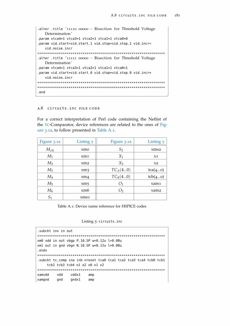
A.8 circuits.inc file code 181
.alter .title ’11110 00000 − Bisection for Threshold VoltageDetermination ’
.param vtca4=1 vtca3=1 vtca2=1 vtca1=1 vtca0=0
.param vid_start=vid_start_1 vid_stop=vid_stop_1 vid_incr=
vid_noise_incr
*****************************************************************.alter .title ’11111 00000 − Bisection for Threshold Voltage
Determination ’.param vtca4=1 vtca3=1 vtca2=1 vtca1=1 vtca0=1
.param vid_start=vid_start_0 vid_stop=vid_stop_0 vid_incr=
vid_noise_incr
*****************************************************************
*****************************************************************.end �a.8 circuits.inc file code
For a correct interpretation of Perl code containing the Netlist ofthe TC-Comparator, device references are related to the ones of Fig-ure 3.1a, to follow presented in Table A.1.
Figure 3.1a Listing 5 Figure 3.1a Listing 5
Mclk xm0 S2 xms2
M1 xm1 X1 x1
M2 xm2 X2 x2
M3 xm3 TCA(4...0) tca(4...0)
M4 xm4 TCB(4...0) tcb(4...0)
M5 xm5 O1 xam1
M6 xm6 O2 xam2
S1 xms1
Table A.1: Device name reference for HSPICE codes
Listing 5: circuits.inc
.subckt inv in out
*****************************************************************xm0 vdd in out vbgp P_10_SP w=0.12u l=0.08u
xm1 out in gnd vbgn N_10_SP w=0.12u l=0.08u
.ends
*****************************************************************.subckt tc_comp ina inb nreset tca0 tca1 tca2 tca3 tca4 tcb0 tcb1
tcb2 tcb3 tcb4 o1 o2 x0 x1 x2
*****************************************************************xamvdd vdd vddx1 amp
xamgnd gnd gndx1 amp
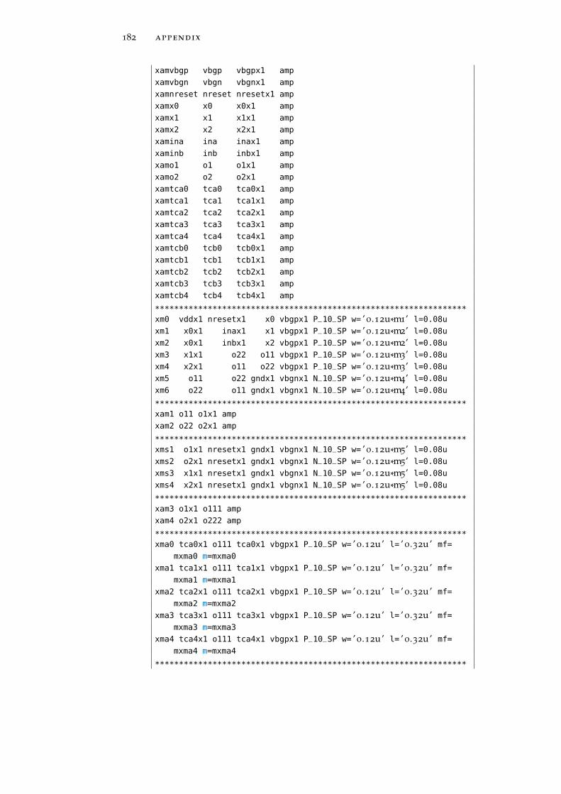
182 appendix
xamvbgp vbgp vbgpx1 amp
xamvbgn vbgn vbgnx1 amp
xamnreset nreset nresetx1 amp
xamx0 x0 x0x1 amp
xamx1 x1 x1x1 amp
xamx2 x2 x2x1 amp
xamina ina inax1 amp
xaminb inb inbx1 amp
xamo1 o1 o1x1 amp
xamo2 o2 o2x1 amp
xamtca0 tca0 tca0x1 amp
xamtca1 tca1 tca1x1 amp
xamtca2 tca2 tca2x1 amp
xamtca3 tca3 tca3x1 amp
xamtca4 tca4 tca4x1 amp
xamtcb0 tcb0 tcb0x1 amp
xamtcb1 tcb1 tcb1x1 amp
xamtcb2 tcb2 tcb2x1 amp
xamtcb3 tcb3 tcb3x1 amp
xamtcb4 tcb4 tcb4x1 amp
*****************************************************************xm0 vddx1 nresetx1 x0 vbgpx1 P_10_SP w= ’ 0.12u*m1’ l=0.08u
xm1 x0x1 inax1 x1 vbgpx1 P_10_SP w= ’ 0.12u*m2’ l=0.08u
xm2 x0x1 inbx1 x2 vbgpx1 P_10_SP w= ’ 0.12u*m2’ l=0.08u
xm3 x1x1 o22 o11 vbgpx1 P_10_SP w= ’ 0.12u*m3’ l=0.08u
xm4 x2x1 o11 o22 vbgpx1 P_10_SP w= ’ 0.12u*m3’ l=0.08u
xm5 o11 o22 gndx1 vbgnx1 N_10_SP w= ’ 0.12u*m4’ l=0.08u
xm6 o22 o11 gndx1 vbgnx1 N_10_SP w= ’ 0.12u*m4’ l=0.08u
*****************************************************************xam1 o11 o1x1 amp
xam2 o22 o2x1 amp
*****************************************************************xms1 o1x1 nresetx1 gndx1 vbgnx1 N_10_SP w= ’ 0.12u*m5’ l=0.08u
xms2 o2x1 nresetx1 gndx1 vbgnx1 N_10_SP w= ’ 0.12u*m5’ l=0.08u
xms3 x1x1 nresetx1 gndx1 vbgnx1 N_10_SP w= ’ 0.12u*m5’ l=0.08u
xms4 x2x1 nresetx1 gndx1 vbgnx1 N_10_SP w= ’ 0.12u*m5’ l=0.08u
*****************************************************************xam3 o1x1 o111 amp
xam4 o2x1 o222 amp
*****************************************************************xma0 tca0x1 o111 tca0x1 vbgpx1 P_10_SP w= ’ 0.12u’ l= ’ 0.32u’ mf=
mxma0 m=mxma0
xma1 tca1x1 o111 tca1x1 vbgpx1 P_10_SP w= ’ 0.12u’ l= ’ 0.32u’ mf=
mxma1 m=mxma1
xma2 tca2x1 o111 tca2x1 vbgpx1 P_10_SP w= ’ 0.12u’ l= ’ 0.32u’ mf=
mxma2 m=mxma2
xma3 tca3x1 o111 tca3x1 vbgpx1 P_10_SP w= ’ 0.12u’ l= ’ 0.32u’ mf=
mxma3 m=mxma3
xma4 tca4x1 o111 tca4x1 vbgpx1 P_10_SP w= ’ 0.12u’ l= ’ 0.32u’ mf=
mxma4 m=mxma4
*****************************************************************
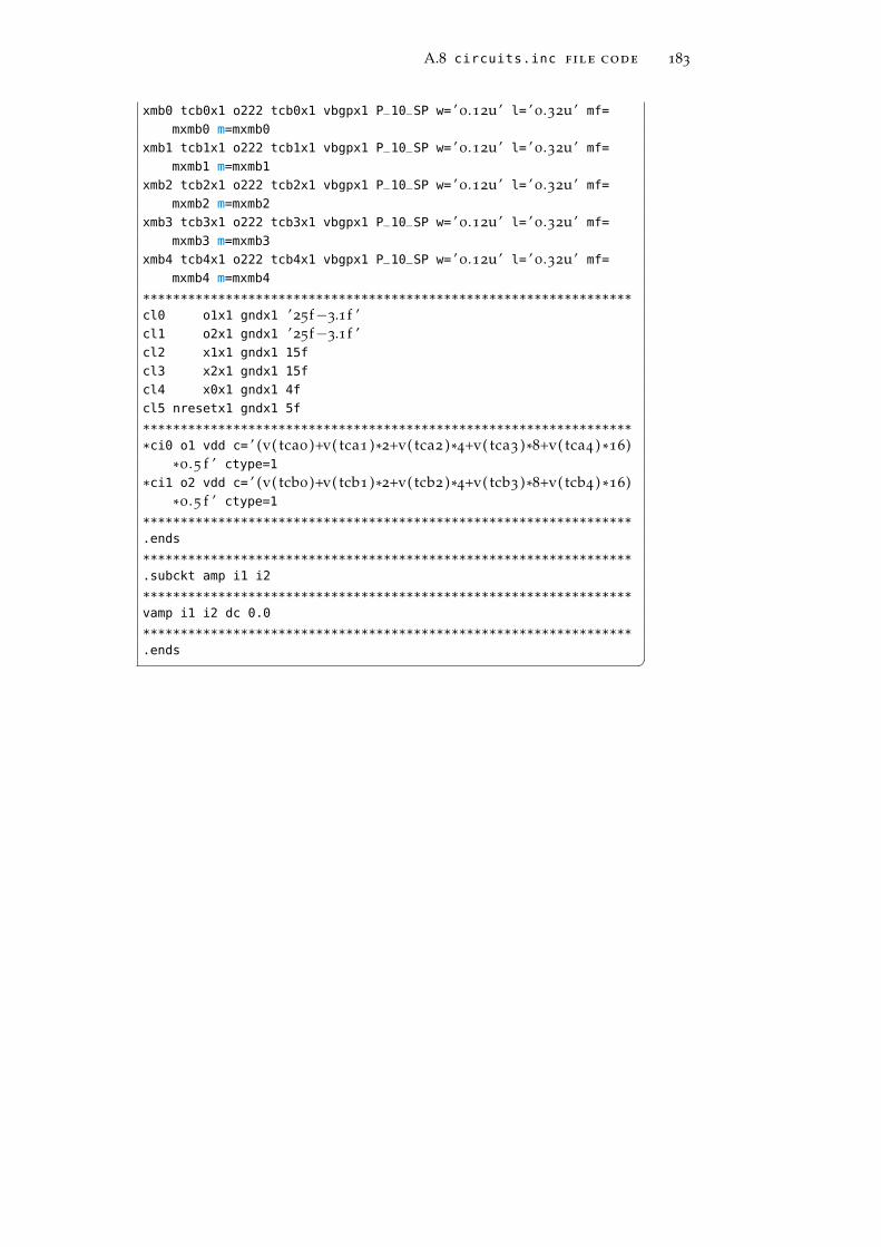
A.8 circuits.inc file code 183
xmb0 tcb0x1 o222 tcb0x1 vbgpx1 P_10_SP w= ’ 0.12u’ l= ’ 0.32u’ mf=
mxmb0 m=mxmb0
xmb1 tcb1x1 o222 tcb1x1 vbgpx1 P_10_SP w= ’ 0.12u’ l= ’ 0.32u’ mf=
mxmb1 m=mxmb1
xmb2 tcb2x1 o222 tcb2x1 vbgpx1 P_10_SP w= ’ 0.12u’ l= ’ 0.32u’ mf=
mxmb2 m=mxmb2
xmb3 tcb3x1 o222 tcb3x1 vbgpx1 P_10_SP w= ’ 0.12u’ l= ’ 0.32u’ mf=
mxmb3 m=mxmb3
xmb4 tcb4x1 o222 tcb4x1 vbgpx1 P_10_SP w= ’ 0.12u’ l= ’ 0.32u’ mf=
mxmb4 m=mxmb4
*****************************************************************cl0 o1x1 gndx1 ’25f−3.1f ’cl1 o2x1 gndx1 ’25f−3.1f ’cl2 x1x1 gndx1 15f
cl3 x2x1 gndx1 15f
cl4 x0x1 gndx1 4f
cl5 nresetx1 gndx1 5f
*****************************************************************
*ci0 o1 vdd c= ’ (v( tca0 )+v( tca1 )*2+v( tca2 )*4+v( tca3 )*8+v( tca4 ) *16)*0 .5 f ’ ctype=1
*ci1 o2 vdd c= ’ (v( tcb0 )+v( tcb1 )*2+v( tcb2 )*4+v( tcb3 )*8+v( tcb4 ) *16)*0 .5 f ’ ctype=1
*****************************************************************.ends
*****************************************************************.subckt amp i1 i2
*****************************************************************vamp i1 i2 dc 0.0
*****************************************************************.ends �

B I B L I O G R A P H Y
[1] G. Temes. “Micropower data converters: A tutorial”. IEEE Trans.Circuits Syst. II, Exp. Briefs, vol. 57(no. 6):pp. 405–410, 2010. (Citedon pages ix, x, and 16.)
[2] L.L. Lewyn, T. Ytterdal, C. Wulff, and K. Martin. “Analog CircuitDesign in Nanoscale CMOS Technologies”. Proceedings of theIEEE, vol. 97(no. 10):pp. 1687–1714, Oct. 2009. (Cited on page ix.)
[3] R. Van de Plassche. “CMOS Integrated Analog–to–Digital andDigital–to–Analog Converters”. Kluwer Academic, 2th edition,2003. (Cited on pages ix, 4, 5, 13, 15, and 18.)
[4] S. Saxena, C. Hess, H. Karbasi, A. Rossoni, S. Tonello, P. McNa-mara, S. Lucherini, S. Minehane, C. Dolainsky, and M. Quar-antelli. “Variation in Transistor Performance and Leakage inNanometer–Scale Technologies”. Electron Devices, IEEE Transac-tions, vol. 55(no. 1):pp. 131–144, Jan. 2008. (Cited on page ix.)
[5] G. Van der Plas and B. Verbruggen. “A 150 MS/s 133µW 7 bitADC in 90 nm Digital CMOS”. IEEE J. Solid–State Circuits, vol. 43
(no. 12):pp. 2631–2640, Dec. 2008. (Cited on pages ix, x, and 24.)
[6] Y.Z. Lin, S.J. Chang, Y.T. Liu, C.C. Liu, and G.Y. Huang. “A5b 800MS/s 2 mW asynchronous binary–search ADC in 65 nmCMOS”. IEEE Int. Solid–State Circuits Conf. Dig. Tech. Papers,pages pp. 80–81, 2009. (Cited on pages ix, 24, and 28.)
[7] M. Chen and R. Brodersen. “A 6b 600 MS/s 5.3 mW asyn-chronous ADC in 0.13”. IEEE J. Solid–State Circuits, vol. 41(no.12):pp. 2669–2680, Dec. 2006. (Cited on pages ix, 20, 21, 27,and 34.)
[8] Craninckx and G. Van der Plas. “a 65 fj/conversion–step 0–to–50
MS/s 0–to–0.7 mw 9b charge–sharing SAR ADC in 90 nm digi-tal CMOS”. IEEE Int. Solid–State Circuits Conf. Dig. Tech. Papers,pages pp. 246–600, Feb. 2007. (Cited on pages ix and 21.)
[9] V. Giannini, P. Nuzzo, V. Chironi, A. Baschirotto, G. Van derPlasand, and J. Craninckx. “An 820 µW 9b 40 MS/s noise–tolerant dynamic-SAR ADC in 90 nm digital CMOS”. IEEE Int.Solid–State Circuits Conf. Dig. Tech. Papers, pages pp. 238–239, Feb.2008. (Cited on pages ix and 21.)
[10] P. Nuzzo, C. Nani, C. Armiento, A. Sangiovanni Vincentelli,J. Craninckx, and G. Van der Plas. “A 6–bit 50–MS/s threshold
185

186 bibliography
configuring SAR ADC in 90–nm digital CMOS”. VLSI Circuits,2009 Symposium, pages pp. 238–239, Jun. 2009. (Cited on pages xand 25.)
[11] P. Nuzzo, C. Nani, C. Armiento, A. Sangiovanni Vincentelli,J. Craninckx, and G. Van der Plas. “A 6–bit 50–MS/s Thresh-old Configuring SAR ADC in 90–nm Digital CMOS”. Circuitsand Systems I: Regular Papers IEEE Transaction, vol. 59(no. 1):pp.80–92, Jan. 2012. (Cited on pages x, 21, 25, 27, 30, 33, 36, 37,and 63.)
[12] A. Hastings. “The art of analog layout”. Prentice Hall, UpperSaddle Riverand, NJ, 2001. (Cited on pages xi and 69.)
[13] V. Navarro-Botello, J. Sosa, and Juan A. Montiel-Nelson. “Anal-ysis and optimization of dinamically reconfigurable regenera-tive comparators for ultra–low power 6–bit TC–ADCs in 90nmCMOS technologies”. in 27th. Intl. Conf. on Design of Circuits andIntegrated Systems (DCIS 2012), Nov. 2012. (Cited on pages xiand 27.)
[14] “SNDR”. http://en.wikipedia.org/wiki/Sndr, Retrieved Au-gust 2012. (Cited on page 8.)
[15] U. Fiedler and D. Seitzer. “A high-speed 8 bit A/D converterbased on a Gray-code multiple forlding circuit”. IEEE Journal ofSolid-State Circuits, vol. SC-14:pp. 547–551, June 1979. (Cited onpage 12.)
[16] R.E.J. van der Grift, W.J.M. Rutten, and M. van der Veen. “An8-bit video ADC incorporating folding and interpolation tech-niques”. IEEE Journal of Solid-State Circuits, vol. SC-22:pp. 944–953, Dec. 1987. (Cited on page 12.)
[17] D. A. Johns and K. Martin. “Analog Integrated Circuit Design”.Wiley, New York, 1997. (Cited on page 15.)
[18] G. C. Temes. “High-accuracy pipeline ADC configuration”. Elec-tron. Lett., vol. 21(no. 17):pp. 762–763, Aug. 1985. (Cited onpage 15.)
[19] “Switched Capacitor”. http://en.wikipedia.org/wiki/
Switched_capacitor, Retrieved August 2012. (Cited onpage 16.)
[20] J.L. McCreary and P.R. Gray. “All-MOS charge distributionanalog-to-digital conversion techniques–Part I”. IEEE J.Solid-State Circuits, vol. SSC-10(no. 6):pp. 371–379, Dec. 1975. (Citedon pages 16 and 20.)

bibliography 187
[21] J.-S. Lee and L.-C. Park. “Capacitor array structure and switchcontrol for energy-efficient SAR ADCs”. Proc. IEEE Int. Symp.Circuits Syst., pages pp. 236–239, 2008. (Cited on page 16.)
[22] K. Lee, J. Chae, M. Aniya, K. Hamashita, K. Takasuka,S. Takeuchi, and G.C. Temes. “A noise-coupled time-interleaveddelta-sigma ADC with 4.2 MHz bandwidth, -98 dB THD, and 79
dB SNDR”. IEEE J.Solid-State Circuits, vol. 43(no. 12):pp. 2601–2612, Dec. 2008. (Cited on page 18.)
[23] J. Markus, J. Silva, and G. C. Temes. “Theory and applicationsof incremental delta-sigma converters”. IEEE Trans. Circuits Syst.I, Reg. Papers, vol. 51(no. 4):pp. 678–690, April 2004. (Cited onpage 18.)
[24] A. Agah, K. Vleugels, P.B. Griffin, M. Ronaghi, J.D. Plummer,and B.A. Wooley. “A high-resolution low-power oversamplingADC with extended-range for bio-sensor arrays”. Proc. IEEE Int.Symp. VLSI Circuits, pages pp. 244–245, June 2007. (Cited onpage 19.)
[25] J. De Maeyer, P. Rombouts, and L. Weyten. “A double-samplingextended-counting ADC”. IEEE J. Solid-State Circuits, vol. 39(no.3):pp. 411–418, March 2004. (Cited on page 19.)
[26] B.P. Ginsburg and A.P. Chandrakasan. “Highly interleaved 5-bit, 250-MSample/s, 1.2-mW ADC with redundant channels in65-nm CMOS”. IEEE J. Solid-State Circuits, vol. 43(no. 12):pp.2641–2650, Dec. 2008. (Cited on pages 20 and 21.)
[27] M. van Elzakker, E. van Tuijl, P. Geraedts, D. Schinkel,E. Klumperink, and B. Nauta. “A 1.9 µW 4.4 fJ/conversion-step10b 1MS/s charge-redistribution ADC”. IEEE Int. Solid-State Cir-cuits Conf. Dig. Tech. Papers, 3-7:pp. 244–610, Feb. 2008. (Cited onpage 21.)
[28] B.P. Ginsburg and A.P. Chandrakasan. “500-MS/s 5-bit ADC in65-nm CMOS with split capacitor array DAC”. IEEE J. Solid-StateCircuits, vol. 42(no. 4):pp. 739–747, Apr. 2007. (Cited on page 21.)
[29] Y.-K. Cho, Y.-D. Jeon, J.-W. Nam, and J.-K. Kwon. “A 9-bit 80
MS/s successive approximation register analog-to-digital con-verter with a capacitor reduction technique”. IEEE Trans. CircuitsSyst. II, Exp. Briefs, vol. 57(no. 7):pp. 502–506, Jul. 2010. (Cited onpage 21.)
[30] F. Kuttner. “A 1.2 V 10b 20 MSample/s non-binary successiveapproximation ADC in 0.13 µm CMOS”. IEEE Int. Solid-State Cir-cuits Conf. Dig. Tech. Papers, vol. 2:pp. 136–137, Feb. 2002. (Citedon page 21.)

188 bibliography
[31] M. Saberi, R. Lotfi, K. Mafinezhad, and W.A. Serdijn.“Analysis of power consumption and linearity in capacitivedigital-to-analog converters used in successive approximationADCs”. IEEE Trans. Circuits Syst. I, Reg. Papers, 2011. doi:10.1109/TCSI.2011.2107214. (Cited on page 21.)
[32] S. Mortezapour and E.K.F. Lee. “A 1-V, 8-bit successive approx-imation ADC in standard CMOS process”. IEEE Journal of Solid-State Circuits, vol. 35:pp. 642–646, April 2000. (Cited on page 21.)
[33] G. Promitzer. “12-bit low-power fully differential switchedcapacitor noncalibrating successive approximation ADC with1MS/s”. IEEE Solid-State Circuits, vol. 36(no. 7):pp. 1138–1143,Jul. 2001. (Cited on page 27.)
[34] T. Kobayashi, K. Nogami, T. Shirotori, and Y. Fujimoto. “Acurrent-controlled latch sense amplifier and a static power-saving input buffer for low-power architectures”. IEEE J. Solid-State Circuits, vol. 28(no. 4):pp. 523–527, Apr. 1993. (Cited onpage 28.)
[35] G. Van der Plas, S. Decoutere, and S. Donnay. “A 0.16
pJ/conversion-step 2.5 mW 1.25 GS/s 4b ADC in a 90 nm digi-tal CMOS process”. IEEE Int. Solid-State Circuits Conf. Dig. Tech.Papers, pages pp. 566–567, Feb. 2006. (Cited on pages 28 and 35.)
[36] P. Nuzzo, G. Van der Plas, F. De Bernardinis, L. Van der Perre,B. Gyselinckx, and P. Terreni. “A 10.6 mW/0.8 pJ power-scalable1 GS/s 4b ADC in 0.18 µm CMOS with 5.8 GHz ERBW”. Proc.IEEE/ACM Design Automation Conf., pages pp. 873–878, Jul. 2006.(Cited on pages 28 and 35.)
[37] B. Wicth, T. Nirschl, and D. Schmitt-Landsiedel. “Yeld andSpeed Optimization of a Latch-Type Voltage Sense Amplifier”.Solid-State Circuits, IEEE Journal on, vol. 39(no. 7):pp. 1148–1158,Jul. 2004. (Cited on pages 31, 36, 37, 63, and 67.)
[38] J. He, S. Zhan, D. Chen, and R. Geiger. “Analyses of static anddynamic random offset voltages in dynamic comparators”. IEEETrans. Circuits Syst. I, Reg. Papers, vol. 56(no. 5):pp. 911–919, May2009. (Cited on pages 31 and 35.)
[39] A. Nikoozadeh and B. Murmann. “An Analysis of Latch Com-parator Offset Due to Load Capacitor Mismatch”. Circuits andSystems II: Express Briefs, IEEE Transactions on, vol. 53(no. 12):pp.1398–1402, Dec. 2006. (Cited on pages 31, 35, and 63.)
[40] S. Nooshabadi and J.A.Montiel-Nelson. “Fast FeedthroughLogic: A high performance Logic Family for GaAs”. Circuitsand Systems I: Reg. Papers, IEEE Transactions on, vol. 51(no. 11):pp.2189–2203, Nov. 2004. (Cited on page 31.)

bibliography 189
[41] V. Navarro-Botello, J.A. Montiel-Nelson, and S. Nooshabadi.“Analysis of high performance fast feedthorugh logic families inCMOS”. Circuits and Systems II: Express Briefs, IEEE Transactionson, vol. 54(no. 6):pp. 489–493, Jun. 2008. (Cited on page 31.)
[42] V. Navarro-Botello, J.A. Montiel-Nelson, and S. Nooshabadi.“Feedthrough: An Energy Efficient CMOS Logic Family forArithmetic Circuits”. CMOS Techonolgy, NOVA Publishers, Elec-trical and Engineering Developments, 2010. (Cited on pages 31
and 69.)
[43] P. Nuzzo, F. De Bernardinis, P. Terreni, and G. Van der Plas.“Noise analysis of regenerative comparators for reconfigurableADC architectures”. IEEE Trans. Circuits Syst. I, Reg. Papers, vol.55(no. 6):pp. 1441–1454, Jul. 2008. (Cited on pages 35, 37, and 69.)
[44] J. Kim, K. Jones, and M. Horowitz. “Fast, non-Monte-Carlo es-timation of transient performance variation due to device mis-match”. IEEE Trans. Circuits Syst. I, Reg. Papers, vol. 57(no. 7):pp.1746–1755, Jul. 2010. (Cited on page 36.)
[45] Ricardo M. Ramos. “Contributions to the design of the energy recov-ery and stabilization system for long range passive wireless sensors”.Tesis Doctoral. Las Palmas de Gran Canaria, 2009. (Cited onpage 45.)
[46] “UMC 90nm LOGIC/MIXED_MODE Standard Performance 1.0VMOSFET SPICE Model (BSIM4V4.3.0 Global Model) Document”.Version 0.6 Phase 1. April 2009. (Cited on page 62.)
[47] R. J. Baker. “CMOS Circuit Design, Layout and Simulation”. Wiley-IEEE, 3th edition, 2010. (Cited on page 140.)
[48] “Nyquist–Shannon sampling theorem”. http://en.wikipedia.
org/wiki/Nyquist-Shannon_sampling_theorem, Retrieved May2013. (Cited on page 141.)
[49] Ulf Grenander. “Probability and Statistics: The Harald Cramer Vol-ume”. Wiley, 1959. (Cited on page 141.)
[50] Harry L. Stiltz. “Aerospace Telemetry”. Prentice-Hall, 1961. (Citedon page 141.)
[51] T. Zawistowski and P. Shah. “An Introduction to Sampling The-ory”. http://www2.egr.uh.edu/~glover/applets/Sampling/
Sampling.html, Retrieved August 2012. (Cited on page 141.)
[52] “Nyquist frequency”. http://en.wikipedia.org/wiki/
Nyquist_frequency, Retrieved August 2012. (Cited on page 141.)

190 bibliography
[53] Weste Neil H.E. and Harris David. “CMOS VLSI Design: A Cir-cuits and Systems Perspective”. Addison Wesley, 3th edition, 2005.ISBN 0-321-14901-7. (Cited on page 142.)
[54] “Process corners”. http://en.wikipedia.org/wiki/Process_
corners, Retrieved September 2012. (Cited on page 142.)
[55] “HSPICE Application Manual”. Version X-2005.09. Synopsys,USA, 2005. (Cited on page 143.)

Friendship.Is not something
you learn in school.But if you haven’t learnedthe meaning of friendship,
you really haven’t learned anything.
— Muhammad Ali
A C K N O W L E D G M E N T S
I would like to thank a lot the Professor Maria Elena Valcher of theDepartment of Information Engineering at University of Padova forher excellent support.
Heartfelt thanks to the Supervisor Dr.D. Juan A. Montiel-Nelson ofthe Department of Telecommunications and Electronic Engineeringat University of Las Palmas de Gran Canaria for his valuable supportand contribution to this work.
191


When you remove the impossible,whatever remains,
however improbable,must be the truth.
— Sherlock Holmes
Padova, October 2013
Roberto Sartori


colophon
This document was typeset using the typographical look-and-feelclassicthesis developed by André Miede. The style was inspiredby Robert Bringhurst’s seminal book on typography “The Elements ofTypographic Style”. classicthesis is available for both LATEX and LYX:
http://code.google.com/p/classicthesis/
Final Version as of October 2, 2013 (classicthesis version 1.2).