Embed Size (px)
Citation preview

DEPARTMENT OF TECHNOLOGY
Design a Highly Linear Power Amplifier Based on HBT
Paul Saad
June 2006
Master’s Thesis in Electronics/Telecommunication Examiner: Prof. Daniel Rönnow

SAAD PAUL M.Sc Thesis 05/06
Design a Highly Linear Power Amplifier Based on SiGe HBT

SAAD PAUL M.Sc Thesis 05/06
Design a Highly Linear Power Amplifier Based on SiGe HBT
ABSTRACT
The RF power amplifier (PA) is one of the critical components in the 802.11 transceivers, and
it is expected to provide a suitable output power at a very good gain with high efficiency and
linearity.
However, present-day telecommunication device technology is not well suited to the
requirements of optical data communication. Digital CMOS is the most used technology in
RF applications, nowadays; nevertheless HBT gives more advantage in terms of higher power
gain and better thermal capabilities.
In this thesis we are designing, manufacturing and testing a power amplifier based on HBT
technology, in order to investigate its characteristics and performance for power amplifier
applications and to prove that HBT power amplifiers can be widely used for this kind of
applications.
Therefore we will study the HBT technology, as well as the transistor characteristics and
HBT structure and properties. Since we are designing a power amplifier for WIFI
applications, we will also give an overview of WIFI and present the IEEE 802.11 physical
layer standard and applications and features of it, and then we will present the advantages and
disadvantages of WIFI and the specifications of the power amplifier to be designed and
manufactured.
This thesis will present a Class A PA design and discuss its performance. We will study
parameters which quantify the various aspects of amplifier performance such as 1-dB
compression point, 3rd order intercept point, intermodulation distortion; efficiency and
adjacent channel power ratio.
The Class A amplifier was designed using NEC HBT (Heterojunction Bipolar Transistor)
transistor models and its performance was simulated using ADS. Various procedures
involved in the design of the Class A amplifier such as DC simulation, bias point selection,
Load-pull characterization, input and output matching circuit design and the design of a bias
network are explained. Memory effects in Power Amplifiers are also discussed and found to
be very small, with less than 0.2 dB variation in the output at fundamental frequencies.
The power gain, linearity, efficiency, power added efficiency, the input and output reflection
coefficients, the Adjacent Channel Power Ratio (ACPR) and the memory effects of the PA

SAAD PAUL M.Sc Thesis 05/06
Design a Highly Linear Power Amplifier Based on SiGe HBT
were measured and have been found to be satisfying and meet the specifications for WIFI
applications. The efficiency of 21% was found, which is in the practical efficiency range for
class A PA. The Linearity of the power amplifier was measured by its two-tone intercept
point and found to be satisfying.
All the results show that this technology can be widely used for this kind of applications and
that HBT can replace CMOS with improve performance, which was our objective.

SAAD PAUL M.Sc Thesis 05/06
Design a Highly Linear Power Amplifier Based on SiGe HBT
Acknowledgment
Working on this thesis was a very useful, important and memorable experience to me. I
would like to thank all those people who made this thesis possible.
To my committee members in the University of Gävle for giving me the opportunity to do my
thesis in Aveiro with such a wonderful committed group of researchers.
To Prof Nuno Borges Carvalho, my advisor at the Institute of Telecommunications, in Aveiro
Portugal. The knowledge that I gained from his lectures and during personal discussions was
invaluable.
To my family, without you, I would have nothing. Without you, I would be nothing. Without
you, I would go nowhere. Thank you!
To my fellow students, I am grateful for the time that we have spent together. As usual I have
learned far more than I expected because of you and will cherish the knowledge as much as
the memories. Keep in touch!
To my friends, you never cease to amaze me. More importantly, you never cease to honor me
with your presence and loyalty. I can hope I have been able to return the favor.

SAAD PAUL v M.Sc Thesis 05/06
Design a Highly Linear Power Amplifier Based on SiGe HBT
Table of Contents
1 CHAPTER 1.................................................................................................................................. 1
INTRODUCTION................................................................................................................................... 1
1.1 BACKGROUND ........................................................................................................................... 1 1.2 THE OBJECTIVE........................................................................................................................ 1
2 CHAPTER 2.................................................................................................................................. 3
HBT TECHNOLOGY............................................................................................................................ 3
2.1 INTRODUCTION ............................................................................................................................. 3 2.2 P-N JUNCTION .............................................................................................................................. 3 2.3 P-N HETEROJUNCTION DIODES ................................................................................................... 4 2.4 THE TRANSISTOR ACTION............................................................................................................ 6 2.5 THE HETEROJUNCTION BIPOLAR TRANSISTOR .......................................................................... 8
2.5.1 Current Gain in HBT............................................................................................................ 8 2.5.2 Basic HBT Structures ......................................................................................................... 12 2.5.3 Advanced HBTs................................................................................................................... 13
2.6 SI-GE HBT VERSUS CMOS........................................................................................................ 16 2.7 CONCLUSION............................................................................................................................... 16
3 CHAPTER 3................................................................................................................................ 17
WI-FI ..................................................................................................................................................... 17
3.1 INTRODUCTION ........................................................................................................................... 17 3.2 WHAT IS WIFI? .......................................................................................................................... 17 3.3 STANDARDS OF WIFI .................................................................................................................. 17 3.4 ADVANTAGES OF WI-FI ............................................................................................................. 19 3.5 DISADVANTAGES OF WI-FI ........................................................................................................ 19 3.6 SPECIFICATIONS FOR 802.11B .................................................................................................... 20
4 CHAPTER 4................................................................................................................................ 21
RF POWER AMPLIFIER THEORY ................................................................................................. 21
4.1 INTRODUCTION ........................................................................................................................... 21 4.2 EFFICIENCY................................................................................................................................. 21

SAAD PAUL vi M.Sc Thesis 05/06
Design a Highly Linear Power Amplifier Based on SiGe HBT
4.3 1-DB COMPRESSION POINT (P1-DB) .............................................................................................. 22 4.4 INTERMODULATION DISTORSION (IMD) ................................................................................... 23 4.5 ADJACENT CHANNEL POWER RATIO (ACPR) .......................................................................... 24 4.6 INTERCEPT POINT (IP) ............................................................................................................... 25 4.7 POWER AMPLIFIER CLASSIFICATION ........................................................................................ 26
4.7.1 Class A................................................................................................................................. 26 4.7.2 Class B................................................................................................................................. 27 4.7.3 Class AB .............................................................................................................................. 28 4.7.4 Class C................................................................................................................................. 29
5 CHAPTER 5................................................................................................................................ 31
DESIGN AND IMPLEMENTATION ................................................................................................. 31
5.1 INTRODUCTION ........................................................................................................................... 31 5.2 MODEL OF THE NEC HBT TRANSISTOR.................................................................................... 31 5.3 BIAS POINT SIMULATION............................................................................................................ 32 5.4 DETERMINATION OF THE S-PARAMETERS................................................................................. 35 5.5 STABILITY ................................................................................................................................... 36 5.6 LOAD PULL ................................................................................................................................. 38 5.7 MATCHING .................................................................................................................................. 40
5.7.1 Input Matching Network .................................................................................................... 40 5.7.2 Output Matching Network .................................................................................................. 41
5.8 BIAS ............................................................................................................................................. 42 5.9 CURRENT SOURCE ...................................................................................................................... 43 5.10 CLASS A IMPLEMENTATION ..................................................................................................... 44 5.11 RESULTS .................................................................................................................................... 45
5.11.1 Single-tone Simulation ..................................................................................................... 45 5.11.2 Two-Tone Simulation ....................................................................................................... 48
5.12 PERFORMANCE OF THE PA IN DIFFERENT CLASSES OF OPERATION ....................................... 50 5.13 LAYOUT..................................................................................................................................... 57
6 CHAPTER 6................................................................................................................................ 59
MEMORY EFFECTS IN POWER AMPLIFIER .............................................................................. 59
6.1 INTRODUCTION ........................................................................................................................... 59 6.2 SOURCES OF MEMORY EFFECTS ................................................................................................ 59

SAAD PAUL vii M.Sc Thesis 05/06
Design a Highly Linear Power Amplifier Based on SiGe HBT
6.2.1 Self-Heating of Active Power Device.................................................................................. 60 6.2.2 Bias Network Construction................................................................................................. 60 6.2.3 Power Supply Properties ..................................................................................................... 60
6.3 SIMULATED RESULTS OF MEMORY EFFECTS IN THE POWER AMPLIFIER ............................... 62
7 CHAPTER 7................................................................................................................................ 67
MEASUREMENTS ............................................................................................................................. 67
7.1 INTRODUCTION ........................................................................................................................... 67 7.2 MATCHING MEASUREMENT........................................................................................................ 67 7.3 POWER GAIN AND COMPRESSION CHARACTERISTIC MEASUREMENT..................................... 68 7.4 ADJACENT CHANNEL POWER RATIO MEASUREMENT.............................................................. 70 7.5 EFFICIENCY AND POWER ADDED EFFICIENCY MEASUREMENTS .............................................. 71 7.6 LINEARITY MEASUREMENT ........................................................................................................ 72 7.7 MEMORY EFFECTS ..................................................................................................................... 74
8 CHAPTER 8................................................................................................................................ 77
CONCLUSION AND THE FUTURE WORK................................................................................... 77
8.1 INTRODUCTION ........................................................................................................................... 77 8.2 CONCLUSION............................................................................................................................... 77 8.3 FUTURE WORK ........................................................................................................................... 77
APPENDIX .......................................................................................................................................... 79
MANUFACTURING............................................................................................................................. 79
REFERENCES .................................................................................................................................... 80

SAAD PAUL viii M.Sc Thesis 05/06
Design a Highly Linear Power Amplifier Based on SiGe HBT
Table of Figures
FIGURE 2-1: P-N JUNCTION AND ITS ENERGY BAND DIAGRAM AT EQUILIBRIUM........................................ 3
FIGURE 2-2: DEPLETION REGION OF A P-N JUNCTION................................................................................ 4
FIGURE 2-3:ENERGY BAND DIAGRAMS FOR: (A) AN ISOLATED N-GE AND P-GAAS SEMICONDUCTOR IN
EQUILIBRIUM, AND (B) N-GE AND P-GAAS BROUGHT INTO INTIMATE CONTACT TO FORM AN N-P
HETEROJUNCTION DIODE. ................................................................................................................ 6 FIGURE 2-4: PERSPECTIVE VIEW OF A SILICON P-N-P BIPOLAR TRANSISTOR.............................................. 6
FIGURE 2-5:(A) IDEALIZED ONE-DIMENSIONAL SCHEMATIC OF A P-N-P BIPOLAR TRANSISTOR AND (B) ITS
CIRCUIT SYMBOL (C) IDEALIZED ONE-DIMENSIONAL SCHEMATIC OF AN N-P-N BIPOLAR TRANSISTOR
AND (D) ITS CIRCUIT SYMBOL........................................................................................................... 7 FIGURE 2-6: VARIOUS CURRENT COMPONENTS IN A P-N-P TRANSISTOR UNDER ACTIVE MODE OF
OPERATION. THE ELECTRON FLOW IS IN THE OPPOSITE DIRECTION TO THE ELECTRON CURRENT ..... 8 FIGURE 2-7:(A) SCHEMATIC CROSS SECTION OF AN N-P-N HETEROJUNCTION BIPOLAR TRANSISTOR (HBT)
STRUCTURE. (B) ENERGY BAND DIAGRAM OF A HBT OPERATED UNDER ACTIVE MODE................. 13 FIGURE 2-8: CURRENT GAIN AS A FUNCTION OF OPERATING FREQUENCY FOR AN LNP-BASED HBT.B ... 14
FIGURE 2-9:( A) DEVICE STRUCTURE OF AN N-P-N SI/SIGE/SI HBT. (B) COLLECTOR AND BASE CURRENT
VERSUS VEB FOR A HBT AND BIPOLAR JUNCTION TRANSISTOR (BJT).......................................... 14 FIGURE 2-10: ENERGY BAND DIAGRAMS FOR A HETEROJUNCTION BIPOLAR TRANSISTOR WITH AND
WITHOUT GRADED LAYER IN THE JUNCTION, AND WITH AND WITHOUT A GRADED-BASE LAYER.... 15 FIGURE 4-1:1-DB COMPRESSION POINT .................................................................................................. 23
FIGURE 4-2: INTERMODULATION DISTORTION........................................................................................ 24
FIGURE 4-3: PLOT OF ADJACENT CHANNEL POWER ............................................................................... 24
FIGURE 4-4: PLOT SHOWING THIRD ORDER INTERCEPT POINT ............................................................... 25
FIGURE 4-5: BIASING FOR CLASS A ........................................................................................................ 27
FIGURE 4-6: BIASING FOR CLASS B......................................................................................................... 28
FIGURE 4-7: BIAS FOR CLASS AB ........................................................................................................... 29
FIGURE 4-8: BIAS FOR CLASS C .............................................................................................................. 30

SAAD PAUL ix M.Sc Thesis 05/06
Design a Highly Linear Power Amplifier Based on SiGe HBT
FIGURE 5-1: MODEL OF THE HBT TRANSISTOR ...................................................................................... 31
FIGURE 5-2: COLLECTOR CURRENT VS. COLLECTOR TO EMITTER VOLTAGE............................................ 32
FIGURE 5-3: SCHEMATIC THAT DETERMINES THE BIAS POINT ................................................................ 33
FIGURE 5-4: BIAS POINT SIMULATION FOR CLASS A............................................................................... 34
FIGURE 5-5: CIRCUIT THAT DETERMINES THE S-PARAMETERS ............................................................... 35
FIGURE 5-6: INPUT AND OUTPUT STABILITY CIRCLES ............................................................................. 37
FIGURE 5-7: ONE TONE LOAD PULL SIMULATION.................................................................................... 38
FIGURE 5-8: LOAD PULL ANALYSIS TO DETERMINE LOAD IMPEDANCE FOR MAXIMUM EFFICIENCY ........ 39
FIGURE 5-9: SMITH CHART FOR THE DESIGN OF THE INPUT MATCHING NETWORK.................................. 40
FIGURE 5-10: SMITH CHART FOR THE DESIGN OF THE INPUT MATCHING NETWORK................................ 41
FIGURE 5-11: BIAS CIRCUIT.................................................................................................................... 42
FIGURE 5-12: CURRENT SOURCE ............................................................................................................ 43
FIGURE 5-13: SCHEMATIC OF CLASS A DESIGN....................................................................................... 44
FIGURE 5-14: SCHEMATIC OF THE ONE TONE HARMONIC BALANCE SIMULATION ................................... 45
FIGURE 5-15: CLASS-A POWER GAIN..................................................................................................... 46
FIGURE 5-16: CLASS-A PAE .................................................................................................................. 46
FIGURE 5-17: CLASS-A PIN VS. POUT..................................................................................................... 47
FIGURE 5-18: FUNDAMENTAL AND THIRD HARMONIC ........................................................................... 48
FIGURE 5-19: ZOOMED OUTPUT SPECTRUM SHOWING 3RD, 5TH AND 7TH ORDER IMD PRODUCTS ......... 49
FIGURE 5-20: PLOT OF THE POWER TRANSDUCER GAIN AND THE PAE ................................................... 49
FIGURE 5-21: PLOT OF THE FUNDAMENTALS AND THE THIRD ORDER INTERMODULATION...................... 50
FIGURE 5-22: 3RD ORDER IMD VERSUS BASE CURRENT......................................................................... 51
FIGURE 5-23: POWER GAIN VERSUS INPUT POWER FOR DIFFERENT BASE CURRENT ................................ 52
FIGURE 5-24: FUNDAMENTAL AND THIRD HARMONIC FOR CLASS AB OPERATION.................................. 52
FIGURE 5-25: PLOT OF THE FUNDAMENTALS AND THE THIRD ORDER INTERMODULATION FOR CLASS AB
...................................................................................................................................................... 53 FIGURE 5-26: POWER GAIN VERSUS INPUT POWER FOR DIFFERENT BASE CURRENT ................................ 54
FIGURE 5-27: FUNDAMENTAL AND THIRD HARMONIC FOR CLASS B OPERATION .................................... 54

SAAD PAUL x M.Sc Thesis 05/06
Design a Highly Linear Power Amplifier Based on SiGe HBT
FIGURE 5-28: PLOT OF THE FUNDAMENTALS AND THE THIRD ORDER INTERMODULATION FOR CLASS B
OPERATION .................................................................................................................................... 54 FIGURE 5-29: FUNDAMENTAL AND THIRD HARMONIC FOR CLASS C OPERATION .................................... 55
FIGURE 5-30: PLOT OF THE FUNDAMENTALS AND THE THIRD ORDER INTERMODULATION FOR CLASS C
OPERATION .................................................................................................................................... 55 FIGURE 5-31: ARTWORK COMPONENT.................................................................................................... 57
FIGURE 5-32: PA LAYOUT DESIGN - ADS.............................................................................................. 58
FIGURE 6-1: TYPICAL LOCATION OF THE MEMORY EFFECTS POWER AMPLIFIER...................................... 59
FIGURE 6-2: MEMORY EFFECTS DUE TO POWER SUPPLY VARIATIONS ..................................................... 61
FIGURE 6-3: MEMORY EFFECTS DUE TO MISMATCHING OF EVEN HARMONICS ........................................ 62
FIGURE 6-4: MEASURED UPPER AND LOWER IMD3 AS FUNCTION OF INPUT POWER AND FREQUENCY
SPACING (∆F) OF A TWO-TONE INPUT SIGNAL: (A) CLASS-A, (B) CLASS-AB................................... 63 FIGURE 6-5: MEASURED OUTPUT SIGNAL AT (A) FUNDAMENTAL FREQUENCIES, (B) UPPER AND LOWER
IMD3 AS FUNCTION OF FREQUENCY SPACING (∆F) OF A TWO-TONE INPUT SIGNAL (INPUT POWER =-
6 DBM). ......................................................................................................................................... 64 FIGURE 6-6: SCHEMATIC OF THE LOAD IMPEDANCE................................................................................ 65
FIGURE 6-7: OUTPUT IMPEDANCE........................................................................................................... 65
FIGURE 6-8: SCHEMATIC OF THE SOURCE IMPEDANCE............................................................................ 66
FIGURE 6-9: INPUT IMPEDANCE .............................................................................................................. 66
FIGURE 7-1: SETUP FOR THE MATCHING MEASUREMENT ........................................................................ 68
FIGURE 7-2: INPUT, OUTPUT REFLECTION COEFFICIENTS (S11, S22) AND TRANSMISSION COEFFICIENT
(S21) ............................................................................................................................................. 68 FIGURE 7-3: POWER GAIN SETUP MEASUREMENTS ................................................................................. 68
FIGURE 7-4: POWER GAIN VERSUS INPUT POWER .................................................................................. 69
FIGURE 7-5: OUTPUT POWER VERSUS INPUT POWER.............................................................................. 70
FIGURE 7-6: 3GPP ACPR MEASUREMENT.............................................................................................. 71
FIGURE 7-7: POWER EFFICIENCY AND PAE VERSUS OUTPUT POWER ...................................................... 72
FIGURE 7-8: TWO TONES MEASUREMENT SETUP .................................................................................... 72
FIGURE 7-9: THE TWO FUNDAMENTALS AND THE THIRD ORDER INTERMODULATION PRODUCTS............ 73

SAAD PAUL xi M.Sc Thesis 05/06
Design a Highly Linear Power Amplifier Based on SiGe HBT
FIGURE 7-10: TWO-TONES INTERCEPT POINT ......................................................................................... 74
FIGURE 7-11: MEASURED OUTPUT SIGNAL AT (A) FUNDAMENTAL FREQUENCIES, (B) UPPER AND LOWER
IMD3 AS FUNCTION OF FREQUENCY SPACING (∆F) OF A TWO-TONE INPUT SIGNAL AND INPUT
POWER SWEEPING .......................................................................................................................... 75 FIGURE 7-12: 3D VIEW OF THE DIFFERENCE MEASURED OUTPUT SIGNAL AT (A) FUNDAMENTAL
FREQUENCIES, (B) UPPER AND LOWER IMD3 AS FUNCTION OF FREQUENCY SPACING (∆F) OF A TWO-
TONE INPUT SIGNAL AND INPUT POWER SWEEPING......................................................................... 76 FIGURE 8-1: MULTIPLE STAGE POWER AMPLIFIER .................................................................................. 78

SAAD PAUL xii M.Sc Thesis 05/06
Design a Highly Linear Power Amplifier Based on SiGe HBT
List of Tables
TABLE 3-1: DIFFERENT FEATURES OF STANDARDS IN WIFI .................................................................... 19
TABLE 3-2:SPECIFICATIONS FOR 802.11B............................................................................................... 20
TABLE 5-1:PARAMETERS OF THE HBT TRANSISTOR............................................................................... 32
TABLE 5-2: SIMULATED S-PARAMETERS ................................................................................................ 35
TABLE 5-3: OUTPUT OF THE CURRENT SOURCE ...................................................................................... 43
TABLE 5-4: VALUES AT 1-DB COMPRESSION POINT................................................................................ 47
TABLE 5-5: HARMONIC LEVELS ............................................................................................................. 48
TABLE 5-6:COLLECTOR CURRENT FOR DIFFERENT VALUES OF BASE CURRENT....................................... 51
TABLE 5-7: CHARACTERISTICS OF THE PA IN DIFFERENT CLASSES OF OPERATION ................................. 56

SAAD PAUL 1 M.Sc Thesis 05/06
Design a Highly Linear Power Amplifier Based on SiGe HBT
1 CHAPTER 1
INTRODUCTION
1.1 Background
Data communication using wireless networks such as IEEE 802.11 has found widespread
use for the last few years. The RF power amplifier (PA) is one of the critical components
in the 802.11 transceivers, expected to provide a suitable output power at a very good
gain with high efficiency and linearity.
Present-day telecommunication device technology is not well suited to the requirements
of data communication among and within computers because the computer environment
is much more demanding. It imposes a higher ambient temperature on the devices, and
requires denser packaging and smaller power dissipation per device, as well as a high
degree of parallelism.
The GaAs/AlGaAs device technology is ideally suited to this task; nevertheless, the high
performance follows the high price on the market, which suggests usage of alternative
technologies.
LDMOS\GAN-based power amplifiers are used for very high power RF applications;
therefore they are used for base station power amplifiers.
BJT transistors offer good performance, but are restricted for low frequency applications.
Due to the high volume of digital ICs using CMOS technology, digital CMOS is an
extremely attractive candidate for realizing low-cost RF circuits; hence it is the most used
technology in RF applications, nowadays. However, this process is geared toward
optimizing digital circuit performance which imposes severe restrictions on realizing
high-performance RF circuits in this technology, such as low power and low thermal
capability.
1.2 The Objective
In this work we are designing, manufacturing and testing a power amplifier based on
HBT technology, in order to investigate its characteristics and performance for power
amplifier applications. If we can get good results that would prove that this technology
can be widely used for this kind of applications we can show that HBT can replace

SAAD PAUL 2 M.Sc Thesis 05/06
Design a Highly Linear Power Amplifier Based on SiGe HBT
CMOS, which are mostly used nowadays, since HBT gives more advantage in terms of
higher power gain and better thermal capabilities, i.e. for the same power, CMOS will
dissipate more heat which increases the costs of the cooling systems and the DC power
consumption.

SAAD PAUL 3 M.Sc Thesis 05/06
Design a Highly Linear Power Amplifier Based on SiGe HBT
2 CHAPTER 2
HBT TECHNOLOGY
2.1 Introduction
Since we are designing a power amplifier based on HBT (Hetero junction Bipolar
Transistor) we will study in this chapter the HBT technology. We will start by giving an
overview on the p-n Junction and p-n Hetero-junction since they form the HBT
transistors. Then we move forward to study the transistor action and the HBT structure
and properties. Since the only difference between HBT and BJT (Bipolar Junction
Transistor) transistors is the difference in the emitter-base junction structure we will end
this chapter by a comparison between the HBTs and BJTs transistors.
2.2 P-N Junction
One of the crucial keys to solid state electronics is the nature of the p-n junction. When p-
type and n-type materials are placed in contact with each other, the junction behaves very
differently than either type of material alone. Specifically, current will flow readily in one
direction (forward biased) but not in the other (reverse biased), creating the basic diode.
This non-reversing behavior arises from the nature of the charge transport process in the
two types of materials [1].
Figure 2-1: p-n junction and its energy band diagram at equilibrium
The open circles on the left side of the junction above represent "holes" or deficiencies of
electrons in the lattice which can act like positive charge carriers. The solid circles on the
right of the junction represent the available electrons from the n-type dopant. Near the
junction, electrons diffuse across to combine with holes, creating a "depletion region".

SAAD PAUL 4 M.Sc Thesis 05/06
Design a Highly Linear Power Amplifier Based on SiGe HBT
The energy level sketch above right is a way to visualize the equilibrium condition of the
p-n junction. When a p-n junction is formed, some of the free electrons in the n-region
diffuse across the junction and combine with holes to form negative ions. In doing so they
leave behind positive ions at the donor impurity sites [1].
Figure 2-2: Depletion region of a p-n junction
2.3 P-N Heterojunction Diodes
A p-n heterojunction diode can be formed by using two semiconductors of different band
gaps and with opposite doping impurities. Examples of p-n heterojunction diodes are
Ge/GaAs, Si/SiGe, AlGaAs/GaAs, InGaAs/InAlAs, In-GaP/GaAs, InGaAs/InP, and
GaN/InGaN heterostructures. The heterojunction diodes offer a wide variety of important
applications for laser diodes, light-emitting diodes (LEDs), photodetectors, solar cells,
junction field-effect transistors (JFETs), modulation-doped field-effect transistors
(MODFETs or HEMTs), heterojunction bipolar transistors (HBTs).
Figure 1.3a shows the energy band diagram for an isolated n-Ge and p-GaAs
semiconductor in thermal equilibrium, and Figure 2-3b shows the energy band diagram of
an ideal n-Ge/p-GaAs heterojunction diode. As shown in Figure 2-3b, the energy band
diagram for a heterojunction diode is much more complicated than that of a p-n
homojunction due to the presence of energy band discontinuities in the conduction band
(∆Ec) and valence band (∆Ev) at the metallurgical junction of the two materials. In Figure
2-3b, subscripts 1 and 2 refer to Ge and GaAs, respectively; the energy discontinuity step
arises from the difference of band gap and work function in these two semiconductors.
The conduction band offset at the heterointerface of the two materials is equal to ∆Ec, and
the valence band offset is ∆Ev. The conduction and valence band offsets (∆Ec and ∆Ev)

SAAD PAUL 5 M.Sc Thesis 05/06
Design a Highly Linear Power Amplifier Based on SiGe HBT
can be obtained from the energy band diagram shown in Figure 2-3a, and are given,
respectively, by
∆Ec = q (χ1 − χ2) (2.1)
∆Ev = (Eg2 − Eg1) − ∆Ec = ∆Eg − ∆Ec (2.2)
This shows that the conduction band offset is equal to the difference in the electron
affinity of these two materials, and the valence band offset is equal to the band gap
difference minus the conduction band offset. From Eq. (2.2) it is noted that the sum of
conduction band and valence band offset is equal to the band gap energy difference of the
two semiconductors. When these two semiconductors are brought into intimate contact,
the Fermi level (or chemical potential) must line up in equilibrium. As a result, electrons
from the n-Ge will flow to the p-GaAs, and holes from the p-GaAs side will flow to the n-
Ge side until the equilibrium condition is reached (i.e., the Fermi energy is lined up across
the heterojunction). As in the case of a p-n homojunction, the redistribution of charges
creates a depletion region across both sides of the junction. Figure 2-3b shows the energy
band diagram for an ideal n-Ge/p-GaAs heterojunction diode in equilibrium, and the band
offset in the conduction and valence bands at the Ge/GaAs interface is clearly shown in
this figure. The band bending across the depletion region indicates that a built-in potential
exists on both sides of the junction. The total built-in potential, Vbi, is equal to the sum of
the built-in potentials on each side of the junction [2], i.e,
Vbi = Vb1 + Vb2 (2.3)
Where Vb1 are Vb2 are the band bending potentials in p-Ge and n-GaAs, respectively.

SAAD PAUL 6 M.Sc Thesis 05/06
Design a Highly Linear Power Amplifier Based on SiGe HBT
Figure 2-3:Energy band diagrams for: (a) an isolated n-Ge and p-GaAs semiconductor in
equilibrium, and (b) n-Ge and p-GaAs brought into intimate contact to form an n-p Heterojunction
diode.
2.4 The Transistor Action
A perspective view of a discrete p-n-p bipolar transistor is shown Figure 2.4 the transistor
is formed by starting with a p-type substrate. An n-type region is thermally diffused
through an oxide window into the p-type substrate. A very heavily doped p+ region is then
diffused into the n-type region. Metallic contacts are made to the p+- and n-regions
through the windows opened in the oxide layer and to the p-region at the bottom.
Figure 2-4: Perspective view of a silicon p-n-p bipolar transistor

SAAD PAUL 7 M.Sc Thesis 05/06
Design a Highly Linear Power Amplifier Based on SiGe HBT
An idealized, one-dimensional structure of a p-n-p bipolar transistor is shown in Figure 2-
5a. Normally; the bipolar transistor has three separately doped regions and two p-n
junctions. The heavily doped p+-region is called the emitter (defined as symbol E in the
figure). The narrow central n-region, with moderately doped concentration, is called the
base (symbol B). The width of the base is small compared with the minority-carrier
diffusion length. The lightly doped p-region is called the collector (symbol C).
Figure 2-5b illustrates the circuit symbol for a p-n-p transistor. The current components
and voltage polarities are shown in the figure. The arrows of the various currents indicate
the direction of current flow under normal operating conditions (also called the active
mode). The + and - signs are used to define the voltage polarities. We can also denote the
voltage polarity by a double subscript on the voltage symbol. In the active mode, the
emitter-base junction is forward biased (VEB>0) and the base-collector junction is reverse
biased (VCB<0).
The n-p-n bipolar transistor is the complementary structure of the p-n-p bipolar transistor.
The structure and circuit symbol of an ideal n-p-n transistor are shown in Figures 2-5c
and 2-5d, respectively. The n-p-n structure can be obtained by interchanging p for n and n
for p from the p-n-p transistor. As a result the current flow and voltage polarity are all
reversed.
Figure 2-5:(a) Idealized one-dimensional schematic of a p-n-p bipolar transistor and (b) its circuit
symbol (c) Idealized one-dimensional schematic of an n-p-n bipolar transistor and (d) its circuit
symbol.

SAAD PAUL 8 M.Sc Thesis 05/06
Design a Highly Linear Power Amplifier Based on SiGe HBT
2.5 The Heterojunction Bipolar Transistor
We have considered the heterojunction in Sec.1.2 a heterojunction bipolar transistor
(HBT) is a transistor in which one or both p-n junctions are formed between dissimilar
semiconductors. The primary advantage of an HBT is its high emitter efficiency. The
circuit applications of the HBT are essentially the same as those of bipolar transistors.
However, the HBT has higher-speed and higher-frequency capability in circuit operation.
Because of these features, the HBT has gained popularity in photonic, microwave, and
digital applications. For example, in microwave applications, HBT is used in solid-state
microwave and millimetre-wave power amplifiers, oscillators, and mixers.
2.5.1 Current Gain in HBT
Figure 2-6 shows the various current components in an ideal p-n-p transistor biased in the
active mode (emitter-base junction is forward biased the collector-base junction is reverse
biased). Note that we assume that there are no generation-recombination currents in the
depletion regions. The holes injected from the emitter constitute the current IEP, which is
the largest current component in a well-designed transistor. Most of the injected holes
will reach the collector junction and give rise to the current ICP. There are three base
current components, labelled IBB, IEn, and ICn. IBB corresponds to electrons that must be
supplied by the base to replace electrons recombined with the injected holes (i.e., IBB - IEp -
ICp). IEn corresponds to the current arising from electrons being injected from the base to
the emitter. However, lEn is not desirable. It can be minimized by using heavier emitter
doping or a heterojunction. ICn corresponds to thermally generated electrons that are near
the base-collector junction edge and drift from the collector to the base. As indicated in
the figure, the direction of the electron current is opposite the direction of the electron
flow [3].
Figure 2-6: various current components in a p-n-p transistor under active mode of operation. The
electron flow is in the opposite direction to the electron current

SAAD PAUL 9 M.Sc Thesis 05/06
Design a Highly Linear Power Amplifier Based on SiGe HBT
We can now express the terminal currents in terms of the various current components
described above:
IE = IEp + IEn (2.4)
IC = ICp + ICn (2.5)
IB = IE - IC = IEn + (IEp- ICp) - ICn (2.6)
An important parameter in the characterization of bipolar transistors is the common base
current gain α0. This quantity is defined by
E
Cp
II
≡0α (2.7)
Substituting Eq. (2.4) into Eq. (2.7) yields
⎟⎟⎠
⎞⎜⎜⎝
⎛⎟⎟⎠
⎞⎜⎜⎝
⎛
+=
+=
Ep
Cp
EnEp
Ep
EnEp
Cp
II
III
III
0α (2.8)
The first term on the right-hand side is called the emitter efficiency y, which is a measure
of the injected hole current compared with the total emitter current:
EnEp
Ep
E
Ep
III
II
+=≡γ (2.9)
The second term is called the base transport factor Tα , which is the ratio of the hole
current reaching the collector to the hole current injected from the emitter:
Ep
CpT I
I=α (2.10)
Therefore, Eq. (2.8) becomes
Tγαα =0 (2.11)

SAAD PAUL 10 M.Sc Thesis 05/06
Design a Highly Linear Power Amplifier Based on SiGe HBT
For a well-designed transistor, because IEn is small compared with IEp and ICp is close to
IEP, both Tα and γ approach unity. Therefore, 0α is close to 1.
We can express the collector current in terms of 0α : The collector current can be
described by substituting Eqs. (2.9) and (2.10) into Eq. (2.5):
CnECnEp
TCnCpC IIII
III +=+⎟⎟⎠
⎞⎜⎜⎝
⎛=+= 0α
γγα (2.12)
The collector current for the common-emitter configuration can be obtained by
substituting Eq. (2.6) into Eq. (2.12):
( ) CBOCBC IIII ++= 0α (2.13)
Solving for IC we obtain
00
0
11 ααα
−+
−= Cn
BCI
II (2.14)
We now designate βo as the common-emitter current gain, which is the incremental
change of Ic with respect to an incremental change of IB. From Eq. (2.14), we obtain
10
00 −
=∆∆
≡αα
βB
C
II
(2.15)
The second factor of (2.14) corresponds to the collector-emitter leakage current for IB=0.
Let semiconductor 1 is the emitter and semiconductor 2 is the base of a HBT. We now
consider the impact of the band gap difference between these two semiconductors on the
current gain of a HBT.
When the base-transport factor Tα , is very close to unity, the common-emitter current
gain can be expressed from Eqs. (2.11) and (2.15) as
γ
γγα
γαα
αβ
−=
−≡
−≡
111 0
00
T
T (For 1=Tα ) (2.16)

SAAD PAUL 11 M.Sc Thesis 05/06
Design a Highly Linear Power Amplifier Based on SiGe HBT
The emitter efficiency is given in function of the transistor physics dimensions [3] by Eq.
(2.17)
En
Eo
P
E
LW
Pn
DD
0
1
1
+=γ (2.17)
Substituting from Eq. (2.16) in Eq. (2.17) yields (for n-p-n transistors)
0
0
0
00
1
E
p
Ep
E
n
E pn
LW
np
DD
≈=β (2.18)
Where NB=0
2
n
i
pn
is the impurity doping in the base, NE= 0
2
E
i
nn
is the impurity doping in
the emitter, DE is the diffusion constant of the minority carriers in the emitter, DP is the
diffusion constant of the minority carriers in the collector, LE is the diffusion length of the
minority carriers in the Emitter and W is the width of the depletion region of the base-
collector junction.
The minority carrier concentrations in the emitter and the base using the law of mass
action [3] are given by
( )( ) E
gEVC
E
iE N
KTENNemitterNemittern
P)/exp(2
0
−== (2.19)
( )( )
( )B
gBVC
B
ip N
KTENNbaseNbasen
n/exp''2
0
−== (2.20)
Where Nc and Nv are the densities of states in the conduction band and the valence band,
respectively, and EgE is the band gap of the emitter semiconductor. N'c, N'v, and EgB are the
corresponding parameters for the base semiconductor.
⎟⎟⎠
⎞⎜⎜⎝
⎛ ∆=⎟⎟
⎠
⎞⎜⎜⎝
⎛ −≈
kTE
NN
kTEE
espNN g
B
EgBgE
B
E exp0β (2.21)
This expression illustrates the advantage of a HBT over a BJT since in a homojunction
BJT, ∆Eg = 0 and the exponential factor is unity which means that we have higher
common emitter gain in a HBT than for a BJT for the same doping.

SAAD PAUL 12 M.Sc Thesis 05/06
Design a Highly Linear Power Amplifier Based on SiGe HBT
2.5.2 Basic HBT Structures
Most developments of HBT technology are for the AlxGa1-xAs/GaAs material system.
Figure 2-7a shows a schematic structure of a basic n-p-n HBT. In this device; the n-type
emitter is formed in the wide band gap AlxGa1_x As whereas the p-type base is formed in
the lower band gap GaAs. The n-type collector and n-type sub collector are formed in
GaAs with light doping and heavy doping, respectively. To facilitate the formation of
ohmic contacts, a heavily doped n-type GaAs layer is formed between the emitter contact
and the AlGaAs layer. Due to the large band gap difference between the emitter and the
base materials, the common-emitter current gain can be extremely large. However, in
homojunction bipolar transistors, there is essentially no band gap difference; instead the
ratio of the doping concentration in the emitter and base must be very high. This is the
fundamental difference between the homojunction and the heterojunction bipolar
transistors [3].
Figure 2-7b shows the energy band diagram of the HBT under the active mode of
operation. The band gap difference between the emitter and the base will provide band
offsets at the heterointerface. In fact, the superior performance of the HBT results directly
from the valence-band discontinuity ∆EV, at the heterointerface. ∆EV increases the valence
band barrier height in the emitter-base heterojunction and thus reduces the injection of
holes from the base to the emitter. This effect in the HBT allows the use of a heavily
doped base while maintaining a high emitter efficiency and current gain. The heavily
doped base can reduce the base sheet resistance. In addition; the base can be made very
thin without concern about the punch-through effect in the narrow base region. The punch
through effect arises when the base-collector depletion region penetrates completely
through the base and reaches the emitter-base depletion region. A thin base region is
desirable because it reduces the base transit time and increases the cut-off frequency.
We can prove that since the cutoff frequency ft can be expressed by (2 TτΠ )-1 [3], where
Tτ is the total time of the carrier transit from the emitter to the collector. Tτ Includes the
emitter delay time Eτ , the base transit time Bτ , and the collector transit time Cτ . The most
important delay is the base transit time and it can be expressed by equation (2.22) [3],

SAAD PAUL 13 M.Sc Thesis 05/06
Design a Highly Linear Power Amplifier Based on SiGe HBT
P
B Dw
2
2
=τ (2.22)
Where w is the base width and DP is the diffusion of the minority carrier in the base.
From equation (2.22) we can conclude that with small base width we can achieve high
frequency transistors.
Figure 2-7:(a) Schematic cross section of an n-p-n heterojunction bipolar transistor (HBT)
structure. (b) Energy band diagram of a HBT operated under active mode
2.5.3 Advanced HBTs
In recent years the InP-based (InP/InGaAs or AlInAs/ InGaAs) material systems have
been extensively studied. The InP-based heterostructures had several advantages. The
InP/InGaAs structure has very low surface recombination, and because of higher electron
mobility in InGaAs than in GaAs, superior high-frequency performance is expected. A
typical performance curve for an InP-based HBT is shown in Fig. 2-8. A very high cut-off
frequency of 254 GHz is obtained. In addition, the InP collector region has higher drift
velocity at high fields than that in the GaAs collector. The InP collector breakdown
voltage is also higher than that in the GaAs [3].
Another heterojunction is in the Si/SiGe material system. This system has several
properties that are attractive for HBT applications. Like A1GaAs/GaAs HBTs, Si/SiGe
HBTs have high-speed capability since the base can be heavily doped because of the band
gap difference. The small trap density at the silicon surface minimizes the surface
recombination current and ensures a high current gain even at low collector current.
Compatibility with the standard silicon technology is another attractive feature. Figure 2-

SAAD PAUL 14 M.Sc Thesis 05/06
Design a Highly Linear Power Amplifier Based on SiGe HBT
9a shows a typical Si/SiGe HBT structure. A comparison of the base and collector
currents measured from a Si/SiGe HBT and a Si homojunction bipolar transistor is given
by Fig. 2-9b. The results indicate that the Si/SiGe HBT has a higher current gain than the
Si homojunction bipolar transistor. Compared with GaAs and InP-based HBTs, the
Si/SiGe HBT, however, has a lower cut-off frequency because of the lower nobilities in
Si.
Figure 2-8: Current gain as a function of operating frequency for an lnP-based HBT.B
(a)
Base-emitter bias (V)
(b) Figure 2-9:( a) Device structure of an n-p-n Si/SiGe/Si HBT. (b) Collector and base current versus
VEB for a HBT and bipolar junction transistor (BJT).

SAAD PAUL 15 M.Sc Thesis 05/06
Design a Highly Linear Power Amplifier Based on SiGe HBT
The conduction band discontinuity ∆ΕC, shown in Fig. 2-7b is not desirable, since the
discontinuity will make it necessary for the carriers in the Heterojunction to transport by
means of thermionic emission across a barrier or by tunnelling through it. Therefore, the
emitter efficiency and the collector current will suffer. The problems can be alleviated by
improved structures such as the graded-layer and the graded-base Heterojunction. Figure
2-10 shows an energy band diagram in which the ∆ΕC is eliminated by a graded layer
placed between the emitter and base Heterojunction. The thickness of the graded layer is
Wg.
The base region can also have a graded profile, which results in a reduction of the band
gap from the emitter side to the collector side. The energy band diagram of the graded
base HBT is illustrated in figure 2-10 (dotted line). Note that there is a built-in electric
field biε ; in the quasi-neutral base. It results in a reduction in the minority-carrier transit
time and, thus, an increase in the common-emitter current gain and the cut-off frequency
of the HBT. biε Can be obtained, for example, by varying linearly the Al mole fraction x
of AlxGa1-xAs in the base from x = 0.1 to x = 0 [3].
For the design of the collector layer, it is necessary to consider the collector transit time
delay and the breakdown voltage requirement. A thicker collector layer will improve the
breakdown voltage of the base-collector junction but proportionally increase the transit
time. In most devices for high-power applications, the carriers move through the collector
at their saturation velocities because very large electric fields are maintained in this layer.
Figure 2-10: Energy band diagrams for a heterojunction bipolar transistor with and without graded
layer in the junction, and with and without a graded-base layer

SAAD PAUL 16 M.Sc Thesis 05/06
Design a Highly Linear Power Amplifier Based on SiGe HBT
2.6 Si-Ge HBT versus CMOS CMOS devices offer the advantages of high Ft and Fmax as well as good linearity and
lower voltage operation, due to lower threshold voltages. HBT devices offer the
advantages of excellent noise performance and an improved transconductance. For RF
communications circuits, SiGe HBT consumes much less power than CMOS to achieve
the same level of performance. The density differences for different circuit applications
are also of practical interest. For RF amplifiers SiGe HBT occupy one-quarter to one-
third the area of CMOS circuits of equivalent functionality.
Noise perhaps is the major advantage of SiGe HBT over CMOS for RF design. The 1/f
noise due to carrier trapping –detrapping at interface states and thermal noise due to gate
and channel resistances are both significantly higher in CMOS than in SiGe HBTs. To
reduce them noise, very large CMOS devices and large operating current are often
required.
2.7 Conclusion
After presenting the HBT structure and HBT properties we can summarize our study of
the HBT technology by presenting the advantages of this technology over simple BJT.
The band gap difference between emitter and base in a HBT transistor results in higher
speed, and thus higher operating frequency. The transistor gain is also increased
compared to a BJT, which can then be traded for a lower base resistance, and hence lower
noise.
For the same amount of operating current, HBT has a higher gain, lower RF noise, and
low 1/f noise than an identically constructed BJT. The higher raw speed can be traded for
lower power consumption as well. For the Same functionality HBT circuits occupy less
area than BJT circuits.

SAAD PAUL 17 M.Sc Thesis 05/06
Design a Highly Linear Power Amplifier Based on SiGe HBT
3 CHAPTER 3
WI-FI
3.1 Introduction
Since we are designing a power amplifier for WIFI applications, in this chapter we will
give an overview of WIFI, the standard IEEE 802.11 and its corresponding
improvements, defined by IEEE, applications and features of each standard, the
advantages and disadvantages of WIFI and finally we will state the specifications of the
power amplifier to be designed for WIFI applications.
3.2 What is WIFI?
WiFi is a set of product compatibility standards for wireless local area networks (WLAN)
based on the IEEE 802.11specifications. New standards beyond the 802.11 specifications,
such as 802.16(WiMAX), are currently in the specification period and offer many
enhancements, anywhere from longer range to greater transfer speeds.
WiFi was intended to be used for mobile devices and LANs, but is now often used for
Internet access. It enables a person with a wireless-enabled computer or personal digital
assistant (PDA) to connect to the Internet when in proximity of an access point. The
geographical region covered by one or several access points is called a hotspot. Hotspots
can be found in airport lounges, coffee shops, corporate cafeterias or any other meeting
area within range of a wireless LAN base station. There are thousands of hotspots all over
the world—and more are being added every day [5].
3.3 Standards of WiFi
The Standards of WIFI is being standardized by the Institute of Electrical and Electronics
Engineers (IEEE):
• IEEE 802.11a
• IEEE 802.11b
• IEEE 802.11g
Most Hotspots use 802.11b.

SAAD PAUL 18 M.Sc Thesis 05/06
Design a Highly Linear Power Amplifier Based on SiGe HBT
The WLAN standards started with the 802.11 definition, developed in 1997 by the IEEE.
This base standard allowed data transmission of up to 2 Mbps. Over time, this standard
has been enhanced. These extensions are recognized by the addition of a letter to the
original 802.11 standard, including 802.11a and 802.11b [4].
3.3.1 802.11b
The 802.11b specification was ratified by the IEEE in July 1999 and operates at radio
frequencies in the 2.4 to 2.497 GHz bandwidth of the radio spectrum. The 802.11b
transmitter uses BPSK (Binary Phase Shift Keying) or QPSK (Quadrature Phase Shift
Keying). The modulation method selected for 802.11b is known as complementary direct
sequence spread spectrum (DSSS) using complementary code keying (CCK) making data
speeds as high as 11 Mbps.
3.3.2 802.11a
The 802.11a specification was also ratified in July 1999, but products did not become
available until 2001 so it isn't as widely deployed as 802.11b. 802.11a operates at radio
frequencies between 5.15 and 5.875 GHz and a modulation scheme known as orthogonal
frequency division multiplexing (OFDM) makes data speeds as high as 54 Mbps possible.
3.3.3 802.11g
The 802.11g employ also OFDM. The advantage of this system is that it reduces errors
introduced by multi-path propagation at high data rates. Systems based on OFDM can
offer higher data rates (54Mbps) or longer range at lower data rates compared with
conventional single carrier systems.
The table below summarizes the differentiating features of each standard.
Standard 802.11b 802.11g 802.11a
Purpose Wireless Internet
Access
Wireless Internet
Access
Wireless Internet
Access
Frequency Band 2.4GHz 2.4GHz 5GHz
Maximum data
rate/channel 11 Mbps 54 Mbps 54 Mbps

SAAD PAUL 19 M.Sc Thesis 05/06
Design a Highly Linear Power Amplifier Based on SiGe HBT
Typical range 100 ft at 11 Mbps
300 ft at 1 Mbps
50 ft at 54 Mbps
150 ft at 11 Mbps
40 ft at 54 Mbps
300 ft at 6 Mbps
Devices Laptop computers,
PDAs, cell phones
Laptop
computers
Laptop
computers,
PDAs, cell
phones Table 3-1: Different features of standards in WiFi
3.4 Advantages of WI-FI
• Allows LANs to be deployed without cabling, potentially reducing the costs of
network deployment and expansion. Spaces where cables cannot be run, such as outdoor
areas and historical buildings, can host wireless LANs.
• WiFi products are widely available in the market. Different brands of access points
and client network interfaces are interoperable at a basic level of service.
• Competition amongst vendors has lowered prices considerably since their inception.
• WiFi networks support roaming, in which a mobile client station such as a laptop
computer can move from one access point to another as the user moves around a building
or area.
• Many access points and network interfaces support various degrees of encryption to
protect traffic from interception.
• WiFi is a global set of standards. Unlike cellular carriers, the same WiFi client works
in different countries around the world [5].
3.5 Disadvantages of WI-FI
• The 802.11b and 802.11g flavors of WiFi use the unlicensed 2.4 GHz spectrum,
which is crowded with other devices such as Bluetooth, microwave ovens, cordless
phones (900 MHz or 5.8 GHz are, therefore, alternative phone frequencies one can use if
one has a WiFi network), or video sender devices, among many others. This may cause
degradation in performance. Other devices that use microwave frequencies, such as
certain types of cell phones, can also cause degradation in performance.
• Power consumption is fairly high compared to some other standards, making battery
life and heat a concern.
SAAD PAUL 20 M.Sc Thesis 05/06
Design a Highly Linear Power Amplifier Based on SiGe HBT
• WiFi networks have limited range. A typical WiFi home router using 802.11b or
802.11g might have a range of 45 m (150 ft) indoors and 90 m (300 ft) outdoors. Range
also varies, as WiFi is no exception to the physics of radio wave propagation, with
frequency. WiFi in the 2.4 GHz frequency block has better range than WiFi in the 5 GHz
frequency block, and less range than the oldest WiFi (and pre-WiFi) 900 MHz block.
• Access points could be used to steal personal information transmitted from WiFi
users.
• Interoperability issues between brands or deviations in the standard can cause limited
connection or lower throughput speeds [5].
3.6 Specifications for 802.11b
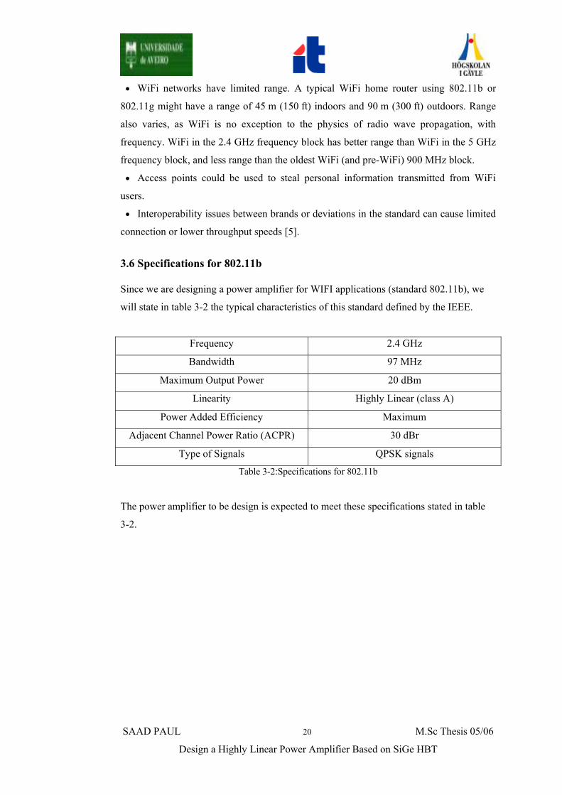
Since we are designing a power amplifier for WIFI applications (standard 802.11b), we
will state in table 3-2 the typical characteristics of this standard defined by the IEEE.
Frequency 2.4 GHz
Bandwidth 97 MHz
Maximum Output Power 20 dBm
Linearity Highly Linear (class A)
Power Added Efficiency Maximum
Adjacent Channel Power Ratio (ACPR) 30 dBr
Type of Signals QPSK signals
Table 3-2:Specifications for 802.11b
The power amplifier to be design is expected to meet these specifications stated in table
3-2.

SAAD PAUL 21 M.Sc Thesis 05/06
Design a Highly Linear Power Amplifier Based on SiGe HBT
4 CHAPTER 4
RF Power Amplifier Theory
4.1 Introduction
The RF power amplifier (PA), a critical element in transmitter units of communication
systems, is expected to provide a suitable output power at a very good gain with high
efficiency and linearity. The output power from a PA must be sufficient for reliable
transmission. High gain reduces the number of amplifier stages required to deliver the
desired output power and hence reduces the size and manufacturing cost. High efficiency
improves thermal management, battery lifetime and operational costs. Good linearity is
necessary for bandwidth efficient modulation. However these are contrasting
requirements and a typical power amplifier design would require a certain level of
compromise. There are several types of power amplifiers which differ from each other in
terms of linearity, output power or efficiency. This thesis will present a Class A PA
design and discuss its performance. Parameters which quantify the various aspects of
amplifier performance such as 1-dB compression point, 3rd order intercept point,
intermodulation distortion; efficiency and adjacent channel power ratio are discussed in
this chapter.
4.2 Efficiency
Commercial RF power amplifiers are designed for high efficiency, resulting in longer
battery life and less complex thermal management. A few figures of merit regarding
efficiency are defined here.
1. Collector efficiency
Collector efficiency η is defined as the ratio of the RF output power and the total DC
consumption power in Eq. 4.1.
DC
out
PP
=η (4.1)

SAAD PAUL 22 M.Sc Thesis 05/06
Design a Highly Linear Power Amplifier Based on SiGe HBT
Where Pout is the total RF output power and PDC is the total DC power consumption.
The collector efficiency is independent of the power gain of the amplifier.
Different classes of operation will have different collector efficiency. The ideal drain
efficiency for Class A is 50%, and 78.5% for Class B. Class C and switching mode
amplifiers have ideally 100% collector efficiency.
2. Power Added Efficiency (PAE)
The power added efficiency (PAE) is defined as
PAEDC
inout
PPP −
= (4.2)
Where Pin is the RF input power. PAE gives the overall efficiency of the power amplifier.
Since
Pout =Pin* Gain (4.3)
PAE= η⎟⎠⎞
⎜⎝⎛ −=⎟
⎠⎞
⎜⎝⎛ −
GainPP
Gain DC
out 1111 (4.4)
This shows that power gain has a large impact on the overall efficiency. The higher the
power gain, the closer PAE is to η. [4]
The PAE is a better figure of merit since in the previous case we can have 100%
efficiency when we have an input of 1 W, an output power of 1 W and a DC power of 1
W which clearly gives a wrong measure of efficiency, the PAE will be 0% in this case.
4.3 1-dB compression point (P1-dB)
When a power amplifier is operated in its linear region, the gain is a constant for a
given frequency. However when the input signal power is increased, there is a
certain point beyond which the gain is seen to decrease. As it’s shown in figure 4-
1.The input 1-dB compression point is defined as the power level for which the

SAAD PAUL 23 M.Sc Thesis 05/06
Design a Highly Linear Power Amplifier Based on SiGe HBT
input signal is amplified 1 dB less than the linear gain. The 1-dB compression
point can be input or output referred and is measured in terms of dBm. A rapid
decrease in gain will be experienced after the 1-dB compression point is reached. This
gain compression is due to the non-linear behavior of the device and hence the 1-dB
compression point is a measure of the linear range of operation.
Figure 4-1:1-dB compression point
4.4 Intermodulation Distorsion (IMD)
Intermodulation distortion is a nonlinear distortion characterized by the appearance, in the
output of a device, of frequencies that are linear combinations of the fundamental
frequencies and all harmonics present in the input signals [5]. A very common procedure
to measure the intermodulation distortion is by means of a two-tone test. In a two-tone
test a nonlinear circuit is excited with two closely spaced input sinusoids. This would
result in an output spectrum consisting of various intermodulation products in addition to
the amplified version of the two fundamental tones and their harmonics. If f1 and f
2 are the
fundamental frequencies then the intermodulation products are seen at frequencies given
by fIMD
= mf1 ± nf
2 , Where m and n are integers from 1 to ∞.
The ratio of power in the intermodulation product to the power in one of the fundamental
tones is used to quantify intermodulation. Of all the possible intermodulation products
usually the third order intermodulation products (at frequencies 2f1-f
2 and 2f
2-f
1) are
typically the most critical as they have the highest strength. Furthermore they often fall in
the receiver pass band making it difficult to filter them out. The fundamentals, the second,
third, fifth and seventh orders are shown in figure 4-2.

SAAD PAUL 24 M.Sc Thesis 05/06
Design a Highly Linear Power Amplifier Based on SiGe HBT
Figure 4-2: Intermodulation Distortion
4.5 Adjacent Channel Power Ratio (ACPR)
In many modern communication systems, the RF signal typically has a modulation band
that fills a prescribed bandwidth on either side of the carrier frequency. Similarly the
intermodulation products also have a bandwidth associated with them. The IM bandwidth
is three times the original modulation band limit for third order products, five times the
band limit for fifth order products and so on. Thus the frequency band of the
intermodulation products from the two tones stretches out, leading to leakage of power in
the adjacent channel. This leakage power is referred to as adjacent channel power. The
adjacent channel power ratio (ACPR) is the ratio of power in the adjacent channel to the
power in the main channel. ACPR values are widely used in the design of power
amplifiers to quantify the effects of intermodulation distortion and hence also serve as a
measure of linearity in real system.
Figure 4-3: Plot of Adjacent Channel Power

SAAD PAUL 25 M.Sc Thesis 05/06
Design a Highly Linear Power Amplifier Based on SiGe HBT
4.6 Intercept Point (IP)
The intercept point is the point where the slope of the fundamental linear component
meets the slope of the intermodulation products on a logarithmic chart of output power
versus input power. Intercept point can be input or output referred. Input intercept point
represents the input power level for which the fundamental and the intermodulation
products have equal amplitude at the output of a nonlinear circuit. In most practical
circuits, intermodulation products will never be equal to the fundamental linear term
because both amplitudes will compress before reaching this point. In those cases intercept
point is measured by a linear extrapolation of the output characteristics for small input
amplitudes. Since the third order intermodulation products, among the IM products, are of
greatest concern in power amplifier design, the corresponding intercept point called the
third order intercept point (IP3) is an important tool to analyze the effects of third order
nonlinearities [5].
Figure 4-4: Plot showing Third Order Intercept point

SAAD PAUL 26 M.Sc Thesis 05/06
Design a Highly Linear Power Amplifier Based on SiGe HBT
4.7 Power Amplifier Classification
There are several types of power amplifiers and they differ from each other in terms of
their linearity, efficiency and power output capability. The first step in designing a power
amplifier is to understand the most important design factor and choose the power
amplifier type most suited for that purpose. For example, linearity and efficiency are the
most important characteristics of the power amplifier design for mobile communication
systems. Beside that high linearity results in poor efficiency and vice versa.
Depending on the linearity and efficiency requirements in the application, the operation
classes of amplifier can be divided into two groups: the first covers high linear amplifiers
such as Pas in mobile communication applications, and the second group belongs to high
efficient amplifiers such as high PAs in satellite applications.
Four operation classes under the first group: class-A, class-B, class –AB and class-C.
These classes are intensively used in power amplifier design for microwave and wireless
mobile communication based on non-constant envelope modulation which use multi-
carrier signals. For this reason, such systems demand highly linear amplification. Beside
that class-D, class-E, class-F, and others, also known as switched mode amplifiers [7],
belong to the second group. These classes are intensively used in power amplifier design
for satellite applications in which very high power is required. Therefore, the efficiency
must be very high in order to avoid high power dissipation in the active device.
In this paragraph, we will consider the first group. These discussions based on BJT
transistor viewpoint.
4.7.1 Class A
Class A is the simplest power amplifier type in terms of design and construction. The
Class A amplifier has a conduction angle of 2π radians or 360°. Conduction angle refers
to the time period for which a device is conducting. Thus a conduction angle of 360º tells
us that in Class A operation the device conducts current for the entire input cycle. Class A
amplifiers are considered to be the most linear since the transistor is biased in the center
of the load line to allow for maximum voltage and current swings without cut-off or
saturation. However the problem with Class A amplifiers is their very poor efficiency.
This is because the device is conducting current at all times which translates to higher
power loss. In fact it can be shown that the maximum efficiency achievable from a Class
A power amplifier is only 50% [8]. However this is a theoretical number and the actual

SAAD PAUL 27 M.Sc Thesis 05/06
Design a Highly Linear Power Amplifier Based on SiGe HBT
efficiency is typically much less. In fact commercial Class A amplifiers have efficiency as
low as 20%. Hence Class A amplifiers are usually used only in places where linearity is a
stringent requirement and where efficiency can be compromised.
Figure 4-5: Biasing for class A
4.7.2 Class B
The next class of power amplifiers is Class B. The transistor is biased at the threshold
voltage point of the transistor for Class B operation. Hence there is a current flowing at
the output of the device only when there is a signal at the input. Moreover the device
would conduct current only when the input signal level is greater than the threshold
voltage. This occurs for the positive half cycle of the input signal and during the negative
half cycle the device remains turned off. Hence the conduction angle for Class B
operation is 180º or π radians. Due to this behavior; there is a large saving in the power
loss. It can be shown that the maximum theoretical efficiency achievable with Class B
operation is about 78.5% [8]. Commercial Class B amplifiers typically have an efficiency
of 40-60%. However, the increased efficiency comes at the cost of reduced linearity. The
reduction in the output power occurs because the output current flows for only one half
cycle of the input signal. The poor linearity is primarily attributed to an effect called the
crossover distortion [8]. Whenever the transistor is turned on (at the start of positive half
cycle) and turned off (at the start of negative half cycle) the transistor does not change
abruptly from one state to the other. Instead the transition is gradual and nonlinear, and
results in an offset voltage. This voltage alters the output waveform (crossover distortion)

SAAD PAUL 28 M.Sc Thesis 05/06
Design a Highly Linear Power Amplifier Based on SiGe HBT
thereby reducing the linearity. Sometimes a Class B amplifier is realized in “push-pull”
configuration. In this configuration the two transistors are driven 180º out-of-phase so
that each transistor is conducting for one half cycle of the input signal and turned off for
the other half cycle.
Figure 4-6: Biasing for class B
4.7.3 Class AB
The crossover distortion effect in Class B amplifiers can be minimized by biasing the
base in such a way so as to produce a small quiescent collector current. This leads to the
type of amplifiers called Class AB, where the transistor is biased between class-A and
class-B. Class AB amplifier operation, as the name suggests, can be considered to be a
compromise between Class A and Class B operation. The conduction angle of a Class AB
amplifier lies between 180º and 360º. By varying the conduction angle the amplifier can
be made to behave more as a Class A or Class B amplifier. Hence the theoretical
maximum efficiency of a Class AB amplifier is between 50% and 78.5%. But commercial
Class AB amplifiers typically have much lower efficiency in the order of 40-55%. Thus a
trade-off between linearity and efficiency can be achieved by simply changing the base
bias. Class AB amplifiers can also be realized in push-pull configurations even though
single transistor configuration is preferred for high frequency linear operation.

SAAD PAUL 29 M.Sc Thesis 05/06
Design a Highly Linear Power Amplifier Based on SiGe HBT
Figure 4-7: Bias for class AB
4.7.4 Class C
In class-C amplifier, the transistor operation point is chosen so that the output current (IC)
is zero for more than one-half duration of the input signal cycle, which means the
conduction angle is less than 180 degree resulting in a good efficiency but on other hand a
poor linearity compared to the previous amplifier classes. The efficiency of a Class C
amplifier depends on the conduction angle. The efficiency increases for decreasing
conduction angle. The maximum theoretical efficiency of a Class C power amplifier is
100%. However this is obtainable only for a conduction angle of 0º which means that no
signal is applied and this condition is of no interest. Commercially Class C amplifiers
typically show an efficiency of 60% or more. Class C amplifiers are widely used in
constant envelope modulation systems where linearity is not an issue.

SAAD PAUL 30 M.Sc Thesis 05/06
Design a Highly Linear Power Amplifier Based on SiGe HBT
Figure 4-8: Bias for class C
As conclusion, increasing the bias current for better linearity (closer to class-A operation)
results in lower efficiency and more heat dissipation. Conversely, lowering the bias
current to improve efficiency (closer to class-B operation) results in reduced linearity. As
soon as the envelope of the signal begins to vary, the linearity of the amplifier becomes
more important so that a more linear amplifier than class-C must be used. In this case
class-A or class-AB is preferred. Although more linear than class-C, the output of class-
AB and class-A amplifiers is still a distorted version of the input.
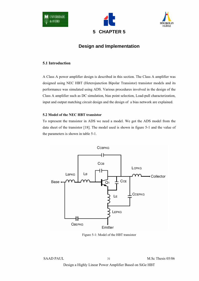
SAAD PAUL 31 M.Sc Thesis 05/06
Design a Highly Linear Power Amplifier Based on SiGe HBT
5 CHAPTER 5
Design and Implementation
5.1 Introduction
A Class A power amplifier design is described in this section. The Class A amplifier was
designed using NEC HBT (Heterojunction Bipolar Transistor) transistor models and its
performance was simulated using ADS. Various procedures involved in the design of the
Class A amplifier such as DC simulation, bias point selection, Load-pull characterization,
input and output matching circuit design and the design of a bias network are explained.
5.2 Model of the NEC HBT transistor
To represent the transistor in ADS we need a model. We got the ADS model from the
data sheet of the transistor [18]. The model used is shown in figure 5-1 and the value of
the parameters is shown in table 5-1.
Figure 5-1: Model of the HBT transistor

SAAD PAUL 32 M.Sc Thesis 05/06
Design a Highly Linear Power Amplifier Based on SiGe HBT
Table 5-1:Parameters of the HBT transistor
5.3 Bias Point Simulation
The first step towards designing the class A amplifier was to select a suitable bias point
for operation. The transistor should be biased for class A operation and maintained
comfortably inside the rectangle limited by the nonlinearity borders which are the
collector-emitter voltage, Knee voltage, Vk, and collector-base breakdown, VBR, and in
current, by collector current cut-off. In that respect, the best quiescent point is the one
exactly located at the geometrical center of the saturation zone rectangle, (point Q in
figure 5-2, since it will allow maximized output linear power, when associated to the
diagonal load-line depicted in the same figure. Such a strategy leads to the widely
accepted rule of thumb that states that a linear power amplifier has its device biased for
class A, at a current close to IC/2 and VCE = (VK+VBR)/2, and is loaded by the output
termination that allows maximized signal excursion without clipping [i.e., an intrinsic RL
not far from RL = (VCE – VK)/IC].
Figure 5-2: Collector current vs. collector to emitter voltage

SAAD PAUL 33 M.Sc Thesis 05/06
Design a Highly Linear Power Amplifier Based on SiGe HBT
In order to determine the bias point simulation a DC bias point simulation was performed.
Figure 5-4 shows that the bias point for a class A should be:
VCE = 75.22
55.02
vK =+
=+ BRv
V
IC = 81.13262.27
2max ==CI
mA which lead to an approximate value of IB = 75 µA.
If we look in figure 5-4 we notice that this point is in the safe operating area of the
transistor. The Safe Operating Area (SOA) of the transistor is defined as the voltage and
current conditions over which the device can be expected to operate without self-damage
due to thermal heating.
The Load at optimal bias RL = Ω=−
=−
9.16281.13
5.05
C
KCE
IVV
The Efficiency %91.4081.1375.2
54.15=
∗==
DC
out
PP
η
All these values are summarized in figure 5.4.
Figure 5-3: Schematic that determines the Bias Point

SAAD PAUL 34 M.Sc Thesis 05/06
Design a Highly Linear Power Amplifier Based on SiGe HBT
Figure 5-4: Bias point simulation for Class A

SAAD PAUL 35 M.Sc Thesis 05/06
Design a Highly Linear Power Amplifier Based on SiGe HBT
5.4 Determination of the S-Parameters
Due to the fact that a class A PA is highly linear, we are able to use S parameters.
Therefore before we start designing the power amplifier we have to determine the S-
parameters of the HBT transistors. The S-parameters are necessary to study the stability
of the transistor by determining the stable and unstable region in the smith chart. We also
need the S-parameters of the transistor to determine the input matching network that
maximizes the power gain. Since the data sheet doesn’t contain the S-Parameters for our
specific bias point, we have to determine the S-parameters. In order to determine the S-
parameters a simulation of the circuit shown in Figure 5-5 was performed.
Figure 5-5: Circuit that determines the S-Parameters
After simulation of the circuit in figure 5.5 we get the S-parameters that are summarized
in the following table.
Table 5-2: Simulated S-parameters
SAAD PAUL 36 M.Sc Thesis 05/06
Design a Highly Linear Power Amplifier Based on SiGe HBT
5.5 Stability
To study the stability of the transistor amplifier we can apply the K – ∆ test, where it can
be shown that a device will be unconditionally stable if Rollet’s condition, defined as
12
1
2112
2222
211 >
∆+−−=
SSSS
K (5.1)
Along with auxiliary condition that
121122211 <−=∆ SSSS (5.2)
are simultaneously satisfied.
We get the S-Parameters of the Transistor from table 5-2
°−∠=°∠=°∠=°∠=
537.138137.0784.36117.0788.65583.4393.168539.0
22
12
21
11
SSSS
62.69519.0788.65583.4784.36117.0537.138137.0393.168539.0 −∠=∠∗∠−−∠∗∠=∆
( ) ( ) ( )( ) 8952.0
536211.02519.0137.0539.01 222
=+−−
=K
Thus we have ∆ < 1, but K < 1, so the unconditional stability criteria are not satisfied, and
the device is potentially unstable.
To find the stability of the transistor we should plot the input and output stability circles
in the Smith Chart.
The input stability circle is defined for 11 11
211222 =
Γ−Γ
+=ΓS
Sout S
SSS and plotted in the Г
S
plane. The centers and radii of the input stability circles are given respectively by:
34.25
65.175236.26**)(
2211
2112
2211
2211
=∆−
=
−∠=∆−
∆−=
SSSR
SSS
C
S
S

SAAD PAUL 37 M.Sc Thesis 05/06
Design a Highly Linear Power Amplifier Based on SiGe HBT
The stable region is defined for 1<Γout so if we set 0ZZ S = , then 0=ΓS
and 22Sout =Γ .
We have 22S = 0.137 1137.0 <=Γ⇒ out so 0=ΓS (centre of the Smith chart) is in
the stable region. The output stability circle is defined for 11 22
211211 =
Γ−Γ
+=ΓL
Lin S
SSS and
plotted in the ГL
plane. The centers and radii of the input stability circles are given
respectively by:
14.2
9.9732.1**)(
2222
2112
2222
1122
=∆−
=
−∠=∆−
∆−=
SSS
R
SSS
C
L
L
The stable region is defined for 1<Γin so if we set 0ZZ S = , then 0=ΓS
and 11Sin =Γ .
We have 11S = 0.539 1539.0 <=Γ⇒ in so 0=ΓS (centre of the Smith chart) is in
the stable region. The input and output stability circles are shown in the right side of
figure 5-6.
The same process is done at other frequencies. We performed a frequency sweeping from
100 MHz to 10 GHz with a step of 100 MHz and we plotted the stability circles at these
frequencies as it is shown in the left side of figure 5-6. We should note that this analysis
is only valid for pure class A power amplifier.
Figure 5-6: Input and output stability circles

SAAD PAUL 38 M.Sc Thesis 05/06
Design a Highly Linear Power Amplifier Based on SiGe HBT
5.6 Load Pull
Load pull is a technique wherein the load impedance seen by the device under test (DUT)
is varied and the performance of the DUT is simultaneously measured [5]. Similarly in
source pull the performance of the DUT for varying source impedances is measured. The
measured results are very useful in determining the optimum load and source impedance
which the device must see to give the best performance. Load pull, in particular, is
commonly used to determine the load impedance required for maximizing efficiency. The
input of a power amplifier is usually conjugate matched to optimize the gain and the
source pull is not always required. It should be noted that the impedance values calculated
vary with bias. In this design, load pull is performed to obtain maximum efficiency. The
load pull schematic is shown in figure 5.7. The results obtained from these simulations
shows that the transistor needs to see an impedance of 65.954 + j*49.007 ohms at the
output in order to get a PAE of 48.81% and get an output power of 11.91 dBm. These
results are shown in figure 5.8.
Figure 5-7: One tone load pull simulation

SAAD PAUL 39 M.Sc Thesis 05/06
Design a Highly Linear Power Amplifier Based on SiGe HBT
Figure 5-8: Load pull analysis to determine load impedance for maximum efficiency
Since we have found the load impedance, we can calculate ГL. ГL is given by
θj
l
lL e
zz
Γ=+−
=Γ11
= 0.41 °∠49 where lz =Zl/50 is the normalized load impedance.
The reflection coefficient seen looking at the input of the transistor is given by
°∠=Γ−Γ
+=Γ 63.16275.01 22
211211
L
Lin S
SSS
Since we have calculated inΓ and in order to get the maximum power transfer from the
input matching network to the transistor we choose 63.16275.0* −∠=Γ=Γ inS .
We notice that LΓ and SΓ are in the stable region of figure 5.6 which implies that the
transistor will be stable and not oscillating. In the next section we will design the input
and output matching sections of the power amplifier.

SAAD PAUL 40 M.Sc Thesis 05/06
Design a Highly Linear Power Amplifier Based on SiGe HBT
5.7 Matching
To match the network we will use an open-circuited shunt stub followed by a length of
transmission line. So, the best way is to work with admittances. It is possible to go from
Z|50Ω
to Y|50Ω
just by rotating the point 180°. We move toward the load on the smith chart
until the circumference whose real part is equal to 1. This will bring us to the 1 +jb circle.
Then we move toward generator from the open circuit point on the smith chart jb to get
the length of the required stub.
5.7.1 Input Matching Network
We plot ГS
= 63.16275.0 ∠ and we do as mention above, we get
Distance to Stub: 0.226λ-0.193 λ=0.033 λ
Length of Stub: 0.184 λ
Figure 5-9: Smith Chart for the design of the input matching network

SAAD PAUL 41 M.Sc Thesis 05/06
Design a Highly Linear Power Amplifier Based on SiGe HBT
5.7.2 Output Matching Network
We plot ГL
= 32.4941.0 ∠ and we do as mention above, we get
Distance to Stub: 0.431λ-0.159λ=0.272λ
Length of Stub: 0.116λ
Figure 5-10: Smith Chart for the design of the input matching network

SAAD PAUL 42 M.Sc Thesis 05/06
Design a Highly Linear Power Amplifier Based on SiGe HBT
5.8 Bias
The SiGe HBT we are using can be biased in several ways. The Bias configuration that
we have chosen for the PA design is represented in the following figure.
Figure 5-11: Bias circuit
In this circuit, the capacitors C1 and C2 represent the DC-Block capacitors.
The capacitors C3, C4 and C5 are used to short the bias feed end. The λ/4 line, TL1,
transforms the short into an open at the frequency 2.4 GHz.
The capacitors C6, C7 and C8 are used to short the bias feed end. The λ/4 line, TL2,
transforms the short into an open at the frequency 2.4 GHz.
The inductors L3 and L4 are used to increase the low frequency stability; if low
frequency passes it will pass to the collector creating a feedback and then the Power
Amplifier could start oscillating at low frequency.

SAAD PAUL 43 M.Sc Thesis 05/06
Design a Highly Linear Power Amplifier Based on SiGe HBT
5.9 Current Source
In order to bias the transistor we need a base current of 75 µA. Since we don’t have a
source current in the laboratory we have to design one. The current source that I have
designed is formed by one npn transistor, one pnp transistor and three resistors as shown
in figure 5.12. The same source voltage that will bias the HBT transistor will bias also
this circuit.
Figure 5-12: Current source
After simulation of this circuit we get the 75 µA at the emitter of the npn transistor, this
will current will bias the base of the HBT transistor.
Table 5-3: Output of the current source

SAAD PAUL 44 M.Sc Thesis 05/06
Design a Highly Linear Power Amplifier Based on SiGe HBT
5.10 Class A Implementation
The various design blocks Matching, Bias and current source of the Class A amplifier
were explained in the previous sections. Figure 5-13 shows the final realization of the
class A power amplifier.
Figure 5-13: Schematic of class A design

SAAD PAUL 45 M.Sc Thesis 05/06
Design a Highly Linear Power Amplifier Based on SiGe HBT
5.11 Results
The Class A amplifier showed in figure 5.13 was simulated in ADS to evaluate its
performance. This was done by means of single-tone and two-tone harmonic balance
simulations.
5.11.1 Single-tone Simulation
A single tone harmonic balance simulation was done to plot the transducer power gain,
the Power Added Efficiency PAE, input power Pin, output power Pout and the harmonic
levels. Figure 5-14 shows the schematic of the one tone harmonic balance simulation.
Figure 5-14: Schematic of the one tone harmonic balance simulation
Figure 5-15 shows the transducer power gain. As expected, gain decreases as the output
power increases. At 1-dB compression point, the gain is about 14.58 dB at 11.57 dBm
output power.

SAAD PAUL 46 M.Sc Thesis 05/06
Design a Highly Linear Power Amplifier Based on SiGe HBT
Figure 5-15: Class-A Power Gain
Figure 5-16 shows the Power Added Efficiency PAE. PAE is directly proportional with
output power, it takes a maximum value of 45.171 at 2 dBm input power and it takes a
value of 42.341 at the 1-dB compression point. Figure 5-17 shows Pout vs. Pin, RF power
means input power and at 10 dBm input power, Pout becomes 10.3 dBm which means 0.3
dB gain. This expected since the amplifier is totally compressed.
Figure 5-16: Class-A PAE

SAAD PAUL 47 M.Sc Thesis 05/06
Design a Highly Linear Power Amplifier Based on SiGe HBT
Figure 5-17: Class-A Pin vs. Pout
All the values at 1-dB compression point are summarized in table 5-4.
Table 5-4: Values at 1-dB compression point
Figure 5-18 shows the spectrum of the fundamental and the Third Harmonic. There is an
important characteristic of the third-order products which makes their presence more of a
problem than one might first imagine. If we look to figure 5.18 in the linear region where
no compression is, we notice that the output from the fundamental signal is proportional
to input, i.e. for 30 dB rise in input level (-40 dBm to -10 dBm) there is 30 dB rise in
output level (-25 dBm to 5dBm). However, the output of the third order product is
proportional to the cube of signal input level and, for a 30 dB change in input level, the
product increases by 90 dB (-140 dBm to -50 dBm).

SAAD PAUL 48 M.Sc Thesis 05/06
Design a Highly Linear Power Amplifier Based on SiGe HBT
Figure 5-18: Fundamental and Third Harmonic
Table 5-5 presents the second, third, fourth and fifth harmonic levels at the output. The
harmonic must be as low as possible in order to avoid unnecessary power loss and
matching issues.
Table 5-5: Harmonic Levels
5.11.2 Two-Tone Simulation
Two-tone harmonic balance simulations were performed on the Class A design.
Harmonic balance is a frequency-domain analysis technique for simulating distortion in
nonlinear circuits. Harmonic balance determines the spectral content of voltages and
currents in the circuit. It is very useful to compute intercept point and intermodulation
distortion. Here the two tone frequencies were chosen to be 2400.05 MHz and 2339.95
MHz. Seventh order harmonic balance simulation was performed to account for all
harmonics up to the seventh harmonic. Fig 5-19 is a zoomed output spectrum of the Class
A PA.
Figure 5-20 shows the Power Gain and the Power Added Efficiency, at the 1-dB
compression point the PAE is 40.047 and is the input power is -4.3 dBm.

SAAD PAUL 49 M.Sc Thesis 05/06
Design a Highly Linear Power Amplifier Based on SiGe HBT
Figure 5-21 shows the two fundamentals, the lower and the upper third intermodulation
distortion. At 1-dB compression point we have the intermodulation distortion is 27 dB
below the fundamentals.
Figure 5-19: Zoomed output spectrum showing 3rd, 5th and 7th order IMD products
Figure 5-20: Plot of the power transducer gain and the PAE

SAAD PAUL 50 M.Sc Thesis 05/06
Design a Highly Linear Power Amplifier Based on SiGe HBT
Figure 5-21: Plot of the fundamentals and the third order intermodulation
5.12 Performance of the PA in different classes of operation
In this section we will study the performance of this power amplifier in other classes of
operation like Classes AB, B and C by changing the bias point only. Since we don’t
change the input and output matching networks of the class A power amplifier, the
amplifier is class A but we will study its characteristics if we let it work in classes AB, B
and C. in order to get a fair comparison between classes we will change the base current
and leave the collector voltage constant and equal to 2.75 V.
We have from figure 5.4 that the maximum collector current is 27.63 mA. The class C is
defined for a collector current less than 1% of this value. This gives that for class C.
IC <0.2734 mA
Table 6.1 gives that the class C is for a base current
IB<1.2 µA
The class B is defined for a collector current between one and 5 percent of this value.
Table 5.6 gives that for class B we have:
0.2734<IC<1.381 mA

SAAD PAUL 51 M.Sc Thesis 05/06
Design a Highly Linear Power Amplifier Based on SiGe HBT
This gives that class B is for a current base between:
1.2<IB<6.2 µA
VCE IB=1 µA
IB=1.2
µA
IB=4 µA
IB=5 µA
IB=6 µA
IB=6.2
µA
2.75 V IC=0.23
mA
IC=0.276
mA
IC=0.908
mA
IC=1.131
mA
IC=1.351
mA
IC=1.395
mA
Table 5-6:Collector current for different values of base current
It is shown in [16] that the PA third harmonic change with the bias point. Class B is
defined for where we have a null in the output third order IMD. Class C would then be
the operating regime of a PA biased below that bias point and classes A and AB would be
the operating regimes of PAs biased above that point. Figure 5.22 shows us the variation
of the third order IMD versus the base current and it is clearly that class B is obtained by
biasing the base by a current of 4 µA. Since class C is for a base current less 1.2 µA we
will choose 1 µA and for class AB we will choose a base current of 20 µA.
Figure 5-22: 3rd order IMD versus Base current
5.12.1 Class AB
For class AB operation the bias point is:
VCE = 2.75 V
IB =20 µA
A single tone and two tones simulations were done to study the characteristics of the PA
in this class. Figure 5-23 shows the transducer power gain in function of the input power

SAAD PAUL 52 M.Sc Thesis 05/06
Design a Highly Linear Power Amplifier Based on SiGe HBT
for different base current. For IB =20 µA the 1-dB compression point is for -13 dBm input
power and 14.18 dB gain. Figure 5-24 shows the fundamental and the third harmonic
which is 29.9 dB below carrier at the 1-dB compression point.
Figure 5.25 shows the two fundamentals, the lower and the upper third intermodulation
distortion. At 1-dB compression point we have the intermodulation distortion is 50.3 dB
below the fundamentals
Figure 5-23: Power gain versus input power for different base current
Figure 5-24: Fundamental and third harmonic for class AB operation

SAAD PAUL 53 M.Sc Thesis 05/06
Design a Highly Linear Power Amplifier Based on SiGe HBT
Figure 5-25: Plot of the fundamentals and the third order intermodulation for class AB
5.12.2 Class B
For class B operation the bias point is:
VCE = 2.75 V
IB =4 µA
A single tone and two tones simulations were done to study the characteristics of the PA
in this class. Figure 5-26 shows the transducer power gain in function of the input power
for different base current. For IB =4 µA the 1-dB compression point is for -23 dBm input
power and 7.9 dB gain. Figure 5-27 shows the fundamental and the third harmonic which
is 37.31 dB below carrier at the 1-dB compression point.
Figure 5.28 shows the two fundamentals, the lower and the upper third intermodulation
distortion. At 1-dB compression point we have the intermodulation distortion is 46.4 dB
below the fundamentals

SAAD PAUL 54 M.Sc Thesis 05/06
Design a Highly Linear Power Amplifier Based on SiGe HBT
Figure 5-26: Power gain versus input power for different base current
Figure 5-27: Fundamental and third harmonic for class B operation
Figure 5-28: Plot of the fundamentals and the third order intermodulation for class B operation

SAAD PAUL 55 M.Sc Thesis 05/06
Design a Highly Linear Power Amplifier Based on SiGe HBT
5.12.3 Class C
For class C operation the bias point is:
VCE = 2.75 V
IB =1 µA
A single tone and two tones simulations were done to study the characteristics of the PA
in this class. Figure 5-26 shows the transducer power gain in function of the input power
for different base current. For IB =1 µA the 1-dB compression point is for -23 dBm input
power and -2.5 dB gain. Figure 5-29 shows the fundamental and the third harmonic which
is 40.6 dB below carrier at the 1-dB compression point.
Figure 5-30 shows the two fundamentals, the lower and the upper third intermodulation
distortion. At 1-dB compression point we have the intermodulation distortion is 35.8 dB
below the fundamentals
Figure 5-29: Fundamental and third harmonic for class C operation
Figure 5-30: Plot of the fundamentals and the third order intermodulation for class C operation

SAAD PAUL 56 M.Sc Thesis 05/06
Design a Highly Linear Power Amplifier Based on SiGe HBT
Table 5-7 shown below summarizes all the values for different classes.
Class A
Class AB Class B Class C
Power Supply
VCE = 2.75 V
IB = 75 µA
IC = 13.9 mA
VCE = 2.75 V
IB = 20 µA
IC = 5.262 mA
VCE = 2.75 V
IB = 4 µA
IC = 0.908 mA
VCE = 2.75 V
IB = 1 µA
IC = 0.23 mA
1-dB
compression
point
-3 dBm
input power
-13 dBm
input power
-23 dBm
input power
-23 dBm
input power
Power Gain @
1-dB
compression
point
14.6 dB 14.16 dB 8.9 dB -2.45 dB
3rd Harmonic
22.45 dBc 29.9 dBc 37.31 dBc 40.6 dBc
Third
Intermodulation
Distortion
27 dBc 50.3 dBc 46.4 dBc 35.8 dBc
Table 5-7: Characteristics of the PA in different classes of operation

SAAD PAUL 57 M.Sc Thesis 05/06
Design a Highly Linear Power Amplifier Based on SiGe HBT
5.13 Layout
The first step in layout design is to create the footprints for each component that is used in
the design. Since we know which components we use, we take the dimensions of these
components from the manufacturer’s data sheet.
Since the 1nF and 1 pF Capacitors have the same dimensions, they are replaced by
C_PAD capacitors from Lumped Artwork with the following characteristics:
mmS
mmLmmW
5.02
2.1
===
The 1 µF Capacitors are replaced by C_PAD capacitors from Lumped Artwork with the
following characteristics:
mmSmmLmmW
143
===
The 1 µH Inductors are replaced by L_PAD inductors from Lumped Artwork with the
following characteristics:
mmSmmLmmW
4.06.18.0
===
Since the Resistors have the same dimensions, they are replaced by R_PAD resistors from
Lumped Artwork with the following characteristics:
mmS
mmLmmW
5.02
2.1
===
Where W is the width of the PAD, L is the pin-to-pin distance and S is the spacing.
Figure 5-31: Artwork component

SAAD PAUL 58 M.Sc Thesis 05/06
Design a Highly Linear Power Amplifier Based on SiGe HBT
The HBT transistor is replaced by the transistor pb_nec_NE68518 _19931201 from the
Library; the transistor used for the current source will be replaced by the transistor
pb_hp_AT32063 _19961111.
The terminations and the voltage source are replaced by the Port component. Port is the
standard port component offered and used to define networks. The number of ports of a
network is the same as the number of Port components connected in it.
After doing the steps described above we start placing the components from the
schematic to the Layout window. The complete Layout is represented in the following
figure.
Figure 5-32: PA Layout Design - ADS

SAAD PAUL 59 M.Sc Thesis 05/06
Design a Highly Linear Power Amplifier Based on SiGe HBT
6 CHAPTER 6
MEMORY EFFECTS IN POWER AMPLIFIER
6.1 Introduction
Electrical systems can be divided into memory less systems and systems with memory.
In Memory less systems, the output signal is only a function of the instantaneous input
signal.
In systems with memory the output signal is a function of both the instantaneous and
previous input signals.
In this chapter we will discuss the sources of the memory effects in Power Amplifiers and
present the simulations done in ADS on our power amplifier to see its performance
against memory effects.
6.2 Sources of Memory Effects
In some references [13], [14], memory effects are categorized as electrical and thermal.
The main source of electrical memory effects is given by bias network impedance
variation. Self-heating effect in the main source of thermal memory effects [13].
Figure 6-1: Typical location of the memory effects power amplifier

SAAD PAUL 60 M.Sc Thesis 05/06
Design a Highly Linear Power Amplifier Based on SiGe HBT
Practically, there are many other additional reasons, which contribute to the memory
effect problem such as dispersion and trapping effects in the power active device.
Mixing all these effects: self-heating, dispersion and trapping effects as well as amplifier
non linearity with additional mismatching, impedance variations and decoupling effects
in the external circuits around amplifier like input and output matching networks, bias
networks and power supply results in that the amplifier output signal is not only a
function of instantaneous input signal value but also a function of previous values.
6.2.1 Self-Heating of Active Power Device
The dissipated power in active devices is the main source of thermal memory effect since
the temperature changes due the dissipated power do not occur instantaneously. The
thermal memory effects can be neglected in low power amplifiers. But this is not the case
for the power amplifiers that are used in the base stations for mobile communications.
6.2.2 Bias Network Construction
The bias networks are required to isolate the RF signal to feed into the bias supply and
avoiding active device instability.
In traditional bias network design, the bias circuit is usually designed to provide relatively
high impedance at RF frequency as compared to the impedances of the input and output
of the device and the matching circuits. In the case of the input signal with non-constant
envelope, the envelope frequency variations cause variation in the impedance of the bias
network which causes nonlinearity variation as a function of envelope frequency
(memory effects).
In an ideal case, to avoid envelope frequency dependent bias network, the impedance
should be a short circuit at envelope frequency and an open circuit at RF frequency to
isolate the RF signal from the bias supply [15]. Practically, it is difficult to realize such an
impedance, which has two requirements that tend to conflict with each other.
6.2.3 Power Supply Properties
In general, the amplifier power supplies are applied to the base and the collector sides in
order to provide the necessary dc voltage or current for active device operation.
Moreover, as described in (chapter 3), different amplifier operation classes give different
output current waveforms with different conduction angles [7].

SAAD PAUL 61 M.Sc Thesis 05/06
Design a Highly Linear Power Amplifier Based on SiGe HBT
Figure 6-2: Memory effects due to power supply variations
Particularly, in the case of the input signal with a non-constant envelope, a current
variation drew from the dc power supply causes dc voltage variations [7]. These voltage
variations however cause additional amplitude modulation of the RF signal (re
modulation) as illustrated in figure 6-2. Moreover, when the impedance of the bias
network is reactive (not short [15]), the additional amplitude modulation will be out of
phase compared to the original RF signal resulting in memory effects or envelope
frequency dependent and asymmetrical of the output signal. To reduce the power supply variation effect in the amplifier, the bias networks should be
carefully designed in order to isolate the current variations drawn from the dc power
supply. Imperfections in the design can increase the variation in the dc voltage and
consequently the memory effects will appear [15].
6.2.4 Mismatching of Even Harmonics
Generally, in the amplifier design, the input/output matching networks are designed to
overcome the mismatching between active nonlinear device (transistor) and input/output
termination (almost 50-ohm) at fundamental frequency. Theoretically, any signal
reflected from the active device at any frequency should be absorbed in the matching
networks but practically; this is not the case in common matching networks [18], because
they are designed at RF amplifier bandwidth (fundamental frequencies) which means
band limited.
Consequently, in the two-tone input signal case, the signals at harmonic zone 0, zone 2,
zone 3, … zone K (figure 6-3) generated from the active device due to its nonlinearity
(first mixing process) are reflected back to the input side rather than absorbed by the input

SAAD PAUL 62 M.Sc Thesis 05/06
Design a Highly Linear Power Amplifier Based on SiGe HBT
matching network resulting. These reflected signals are mixed again in the active device
with the two-tone input signal (second mixing process) and generates an additional
nonlinearity in the output signal as modification of the output spectrum (figure 6-3) [14].
In the second mixing process, it is important to note that, the active device two-tone input
signal is mixed with the reflected signal at even harmonic zones resulting in a
modification of the odd order IMD (zone 2 in figure 6-3) and besides that, mixing the
two-tone input signal with the reflected signal at odd harmonic zones will not result in a
modification of the odd order IMD.
Figure 6-3: Memory effects due to mismatching of even harmonics
As shown in figure 6-3, the resultant 3rd order IMD is a vector sum of the signals at IMD
produced from the 3rd order nonlinearity (first mixing process) and the signals at IMD
produced from the second order nonlinearity (second mixing process) in the active
device.
6.3 Simulated Results of Memory Effects in the Power Amplifier
The simulations were done for class-A and class-AB operation. Operating points were
VCE = 2.75 V, IB = 75 µA for class A and VCE = 2.75 V, IB = 20 µA for class AB.
Two-tone stimulus input signal with center frequency of 2.4 GHz was used. The
frequency spacing was varied between two tones from 10 KHz to 5 MHz and input power
sweep from -18 dBm to 3 dBm was considered. Figures 6-4a and 6-4b shows that in both
classes, the output signal at the third order intermodulation don’t have a power variation
as function of the envelope frequency, which means that, this power amplifier doesn’t
exhibit memory effects.

SAAD PAUL 63 M.Sc Thesis 05/06
Design a Highly Linear Power Amplifier Based on SiGe HBT
(a)
(b)
Figure 6-4: Measured upper and lower IMD3 as function of input power and frequency spacing
(∆f) of a two-tone input signal: (a) class-A, (b) class-AB
.
Figure 6-5 shows the measured memory effects in the HBT Power Amplifier device at
fundamental output powers and third intermodulation for class-A operation. We can
notice that this power amplifier have low memory effects since it shows
• Less than 0.01dB variation in the output power at fundamental frequencies.
• Less than 0.2 dB variations in the third order IMD.
(a)

SAAD PAUL 64 M.Sc Thesis 05/06
Design a Highly Linear Power Amplifier Based on SiGe HBT
(b)
Figure 6-5: Measured output signal at (a) fundamental frequencies, (b) upper and lower IMD3 as
function of frequency spacing (∆f) of a two-tone input signal (input power =-6 dBm).
We notice that the highest memory effect is located at frequency spacing of 158.6 KHz.
Since the HBT device is of small size, we do not expect significant heating or power
dissipation and, thus, we do not expect that the memory arises from thermal heating.
This phenomena is explained in [16], it is proved that if the information bandwidth spans
from dc to a few MHz and the impedance of the base-band matching network changes
over that frequency range, the PA response over that same bandwidth will present some
kind of memory effects that can be visible in the variation of the IMD when performing
two-tone tests with different frequency separation.
To prove that the impedance of the base-band matching network changes over the
frequency range of the information bandwidth we have performed a simulation of the
load impedance shown in figure 6-6 and of the source impedance shown in figure 6-8.
The load and source impedances simulated for frequencies from 1 MHz to 20 MHz are
shown in figures 6-7 and 6-9 respectively.
We notice from these plots important variations of the impedances with resonance
situated around of 158.6 KHz.

SAAD PAUL 65 M.Sc Thesis 05/06
Design a Highly Linear Power Amplifier Based on SiGe HBT
Figure 6-6: Schematic of the load impedance
Figure 6-7: Output impedance

SAAD PAUL 66 M.Sc Thesis 05/06
Design a Highly Linear Power Amplifier Based on SiGe HBT
Figure 6-8: Schematic of the source impedance
Figure 6-9: Input impedance

SAAD PAUL 67 M.Sc Thesis 05/06
Design a Highly Linear Power Amplifier Based on SiGe HBT
7 CHAPTER 7
MEASUREMENTS
7.1 Introduction
An essential part of every circuit design is the measurement of an IC chip. The physical
manifestation of a circuit design is often very different from even the most detailed and
intricate simulations. For power amplifiers, which are perhaps the most empirical of all
RF designs, this is especially true. This chapter will discuss the specifics of measuring
this power amplifier design. The power gain, filtered output power, linearity,
efficiency, power added efficiency, the input and output reflection coefficients and
the memory effects of the PA were measured and are presented in the following
sections.
7.2 Matching measurement
Matching of the circuit was measured by its input and output reflection coefficients using
a Vector Network Analyzer, VNA, and a source voltage in order to bias the power
amplifier in class A as is shown in figure 7-1. A perfect match at the output or input of a
circuit would imply a zero reflected power at the two ports. S11 and S22 of -10 dB
suggest an acceptable level of matching. A lower value than -10 dBm for the reflection
coefficients implies a good match. Figure 7-2 illustrates the input and output reflection
coefficients of the circuit versus frequency. S22 is below -10 dB and S11 is below -20 dB
over a wide band of 200 MHz approximately which mean that we have a very good
match.
Figure 7-2 shows also the gain S21 of the PA which is the transmitted power from the
input port to the output port. We notice a wide band gain around our frequency of interest
of 17 dB approximately.

SAAD PAUL 68 M.Sc Thesis 05/06
Design a Highly Linear Power Amplifier Based on SiGe HBT
Figure 7-1: Setup for the matching measurement
Figure 7-2: Input, output reflection coefficients (S11, S22) and transmission coefficient (S21)
7.3 Power Gain and Compression Characteristic Measurement
Power Gain of the amplifier was measured using the setup shown in figure 7-3. The
spectrum analyzer is employed in the test setup to measure the power spectrum of the
Fundamental frequency generated by the signal generator, the power supply is used to
bias the power amplifier in class A.
Figure 7-3: Power Gain setup measurements

SAAD PAUL 69 M.Sc Thesis 05/06
Design a Highly Linear Power Amplifier Based on SiGe HBT
To calculate the power gain we perform a power sweep from -30 dBm to 0 dBm with 0.5
dB step. For each input power we read the output power from the spectrum analyzer, we
substrate the input power from the output power and hence we get the power gain. Figure
7.4 shows the power gain versus the input power.
Figure 7-4: Power Gain versus Input Power
Every power amplifier gets saturated after a certain input power. The PA was measured
for its compression point. The output 1 dB compression point of the class A power
amplifier was measured at 2.4 GHz with a 2.75 V power supply. Figure 7-5 shows the
output power versus the input power of the power amplifier. The output 1 dB
compression point is shown in figure 7-4 and in figure 7-5 to be approximately at -6.5
dBm input power and +8.468 dBm output power.

SAAD PAUL 70 M.Sc Thesis 05/06
Design a Highly Linear Power Amplifier Based on SiGe HBT
Figure 7-5: Output Power versus Input Power
7.4 Adjacent Channel Power Ratio Measurement
The Adjacent Channel Power Ratio (ACPR) of the amplifier was measured using the
setup shown in figure 7-3. Adjacent channel power ratio (ACPR) characterizes how the
main channel power spills over into the adjacent channels due to the nonlinearity of the
PA. The problem that we have faced in this measurement was that our signal generator
doesn’t generate WIFI signals. We have performed this measurement with 3GPP
WCDMA signals. The power in the WCDMA carrier is measured using a 5MHz
measurement bandwidth. The total power in the adjacent channel and in the alternate
from the center of the outermost carrier is measured and compared to the carrier power.
The result is expressed in dBc.
For the adjacent channel we got -54 dBc and for the alternate channel we got -60 dBc
which meet with the specifications for 3GPP and the specifications of WIFI and imply
that we have a good linearity.

SAAD PAUL 71 M.Sc Thesis 05/06
Design a Highly Linear Power Amplifier Based on SiGe HBT
Figure 7-6: 3GPP ACPR measurement
7.5 Efficiency and Power Added Efficiency measurements
Power conversion efficiency of the PA was also measured under the same conditions with
a 2.75v power supply at 2.4 GHz. The efficiency was measured by taking the ratio of the
output power seen on the spectrum analyzer to the total DC power consumed from the
power supply. The power added efficiency was measured by taking the ratio of the output
power seen on the spectrum analyzer minus the input power to the total DC power
consumed from the power supply. Figure 7-7 shows the efficiency (red) and the power
added efficiency (blue) of the power amplifier versus the output power of the circuit. As
the output power increases, the PAE and the Efficiency also increases. A maximum
power efficiency of almost 28.4% was measured and a maximum PAE of 26% was
measured when the input power is -0.5 dBm.
We notice that at 1-dB compression point the power efficiency is approximately 21.3%
and the power added efficiency is 20.62%

SAAD PAUL 72 M.Sc Thesis 05/06
Design a Highly Linear Power Amplifier Based on SiGe HBT
Figure 7-7: Power efficiency and PAE versus output power
7.6 Linearity measurement
Linearity of the power amplifier was measured by its two-tone intercept point. The
measurement setup is shown in figure 7-8. For accurate measurement, the power loss of
the power combiner, the cables and the connectors were measured in advance.
Figure 7-8: Two Tones measurement setup
Two closely spaced equal amplitude input tones were applied to the circuit at 2.4 GHz
and 2.4001 GHz. The intermodulation products of the two signals would lie at 2.3999
GHz and 2.4002 GHz. These two intermodulation products are hard to filter out because

SAAD PAUL 73 M.Sc Thesis 05/06
Design a Highly Linear Power Amplifier Based on SiGe HBT
they are in the operating band of the amplifier. Figure 7-9 shows the fundamental and
intermodulation products at the output versus the input power. We notice that the 1-dB
compression point now is around -10 dBm input power, which is 3 dB below the 1-dB
compression point of the one tone measurement.
Figure 7-9: The two fundamentals and the third order intermodulation products
The two-tone intercept point of the PA was measured to be 16 dBm at the output and 1
dBm per tone at the input this measurement is done by linear extrapolation of the
fundamentals and the third order intermodulation products as shown in figure 7-10.

SAAD PAUL 74 M.Sc Thesis 05/06
Design a Highly Linear Power Amplifier Based on SiGe HBT
Figure 7-10: Two-Tones intercept point
7.7 Memory Effects
Memory effects of the PA were also measured under the same conditions and same setup
measurement of the linearity measurement shown in figure 7-8. Two-tone stimulus input
signal with centre frequency of 2.4 GHz was used. The frequency spacing was varied
between two tones from 10 KHz to 2MHz and the input power is swept from -30 dBm to
0 dBm.
Figure 7-11 shows the measured memory effects in the Power Amplifier device at
fundamental output powers and third intermodulation for class-A operation. Figure 7-12
shows the difference between the two fundamentals and the difference between the third
order intermodulation products in 3D view. We can notice that this power amplifier have
low memory effects since it shows
• Less than 0.2 dB variation in the output power at fundamental frequencies.
• Less than 1.5 dB variations in the third order IMD.

SAAD PAUL 75 M.Sc Thesis 05/06
Design a Highly Linear Power Amplifier Based on SiGe HBT
(a)
(b)
Figure 7-11: Measured output signal at (a) fundamental frequencies, (b) upper and lower IMD3 as
function of frequency spacing (∆f) of a two-tone input signal and input power sweeping

SAAD PAUL 76 M.Sc Thesis 05/06
Design a Highly Linear Power Amplifier Based on SiGe HBT
(a)
(b)
Figure 7-12: 3D View of the difference measured output signal at (a) fundamental frequencies, (b)
upper and lower IMD3 as function of frequency spacing (∆f) of a two-tone input signal and input
power sweeping

SAAD PAUL 77 M.Sc Thesis 05/06
Design a Highly Linear Power Amplifier Based on SiGe HBT
8 CHAPTER 8
CONCLUSION AND THE FUTURE WORK
8.1 Introduction
There are many issues surrounding power amplifier design that can make or break
practical implementation. Given the empirical nature of power amplifier design, there are
many issues that should be explored in future work. This chapter gives a brief overview
of some of these issues and gives some conclusions for this research.
8.2 Conclusion
The primary goal of the project, that HBT transistors can replace widely used CMOS
technology in RF applications, has been fulfilled in the modelling of an HBT power
amplifier. Based on the results we got, HBT technology gives more advantage in terms of
higher power gain and better thermal capabilities, than CMOS.
Many aspects of the PA were considered when presenting the final results, as the power
gain, filtered output power, linearity, efficiency, power added efficiency, the input and
output reflection coefficients and the memory effects.
At 1-dB compression point the power efficiency found is approximately 21.3% and the
power added efficiency is 20.62%, which meets the practical efficiency of the class A
Power Amplifiers. Linearity of the power amplifier was measured by its two-tone
intercept point, and showed good results, and we can also notice that this power amplifier
has low memory effects since it shows less than 0.2 dB variations in the output power at
fundamental frequencies.
In overall, this gives a solid base for the future work in popularization of the HBT based
PA.
8.3 Future Work
Future work related to the topics and innovations presented in this thesis can be divided
into two categories: theoretical research and practical areas. The first includes all issues
related to modelling, analysis and extraction, and partially those related to simulations

SAAD PAUL 78 M.Sc Thesis 05/06
Design a Highly Linear Power Amplifier Based on SiGe HBT
and measurements, while the latter is considered here to include real world problems in
PAs that can be solved by the circuit techniques.
Several research directions for the future work, using this thesis as a starting point can be
identified:
• increasing the efficiency and the PAE more with increasing the IMD performance
at the same time
• understanding the sources of the memory effects and try to minimize them
• optimizing the design to get best results
One of the possible directions in the future work is multiple stage PA design.
In any practical PA implementation, multiple stages are necessary to amplify the signal
from the small- signal regime to a high power level. This is implemented in multiple
stages, as illustrated in Fig. 8.1, with each stage providing on the order of 10 dB of power
gain.
Figure 8-1: Multiple stage power amplifier
It is believed that the future development of a HBT PAs with many more elements
and active devices integrated, is able to provide an increase in gain for signals as well
as better performance in RF applications.
As such, further work can be aimed at producing inexpensive and well-manufactured
applications for the purpose of power combining and amplification.

SAAD PAUL 79 M.Sc Thesis 05/06
Design a Highly Linear Power Amplifier Based on SiGe HBT
Appendix
Manufacturing We printed out the design on a paper then we took a photo with a special machine to get
the circuit on a film. We notice that we have printed the layout in the dark field polarity
(negative process). Then we have followed the following steps.
• Put the film on the board and let it be subject to Ultraviolet rays for about 40 to 60
seconds. The ultraviolet rays will fix the copper where the film is transparent.
• Plunge the board in a chemical solution for about 10 minutes to remove the unusable
copper from the board and get our circuit.
• Let the board to be subject to ultraviolet rays to dry it on the both sides.
• Solder the components of the circuits (Transistors, Resistances, Capacitors, Inductors
and Connectors).
The following figure shows the final power amplifier board.

SAAD PAUL 80 M.Sc Thesis 05/06
Design a Highly Linear Power Amplifier Based on SiGe HBT
References [1] http://hyperphysics.phy-astr.gsu.edu/hbase/solids/pnjun.html
[2] Sheng S. Li, “Semiconductor Physical Electronics”, Plenum, New York, 1993
[3] S.M.Sze, “Semiconductor Devices Physics and Technology”, 2nd Edition, John
Wiley & Sons, New York, INC., 2001
[4] http://www.cellular.co.za/wifi.htm
[5] http://www.answers.com/topic/wifi
[6] Peter B. Kenington, “High-linearity RF amplifier design”, Artech House,
INC., 2000.
[7] S.C. Cripps, “RF Power Amplifiers for Wireless Communications”, Artech
House, Norwood, MA, 1999.
[8] H.L. Krauss, C.W. Bostian and F.H. Raab, “Solid State Radio Engineering”,
John Wiley & Sons, New York, NY 1980.
[9] N. Sokal and A. Sokal, Class E-A New Class of High-Efficiency Tuned Single
Ended Switching Power Amplifiers, “IEEE Journal of Solid State Circuits”, Vol.
SC10, June 1975, pp. 168-76.
[10] M. Albulet, “RF Power Amplifiers”, Noble Publishing, Atlanta, GA, 2001.
[11] Jose Carlos Pedro and Nuno Borges Carvalho, “Intermodulation Distortion in
Microwave and Wireless Circuits”, Artech House, INC., 2003.
[12] David M.Pozar, “Microwave Engineering”, John Wiley & Sons, INC., 2005.

SAAD PAUL 81 M.Sc Thesis 05/06
Design a Highly Linear Power Amplifier Based on SiGe HBT
[13] A. Ahmed, M. Endalkachew, and G. Kompa: Power Amplifier Linearization
Using Memory Polynomial Predistorters with Non-uniform Delay Taps, “IEEE
MTT-S Int. Microwave Symp. Dig. ”, Fort Worth, TX, USA, June 2004, pp. 1871-
1874.
[14] J. Vuolevi and T. Rahkonen, “Distortion in RF Power Amplifier”, Norwood,
MA: Artech House, 2003.
[15] A. Khanifar, N. Maslennikov, and B. Vassilakis: Bias Circuit Topologies for
Minimization of RF Amplifier Memory Effects, “33rd European Microwave
Conference”, Germany, October 2003, pp. 1349-1352
[16] Pedro Miguel Cabral, Jose Carlos Pedro and Nuno Borges Carvalho, “A
unified Theory for Nonlinear Distortion Characteristics in Different Amplifier
Technologies”, Instituto de telecomunicações Aveiro, 2005.
[17] Kate A. Remley, Dylan F. Williams, Dominique M. M., P. Schreurs and John
Wood Jose, “Simplifying and Interpreting Two-Tone Measurements”, IEEE
Transactions on Microwave Theory and Techniques, VOL. 52, N0.11, November
2004
[18] http://www.cel.com/pdf/datasheets/nesg2031m05.pdf