Embed Size (px)
Citation preview
A 180mW InP HBT Power Amplifier MMIC at 214 GHz
Thomas B. Reed1, Zach Griffith2, Petra Rowell2, Mark Field2, Mark Rodwell1, Fellow, IEEE 1University of California, Santa Barbara
Department of Electrical and Computer Engineering
Santa Barbara, CA, 93106-9560 USA
2Teledyne Scientific and Imaging
1049 Camino Dos Rios, Thousand Oaks, CA, USA 91360
Abstract — A solid state power amplifer MMIC is
demonstrated with 180mW of saturated output power at 214GHz, from an unthinned die, and a small signal S21 gain of 22.0dB. 3-dB
bandwidth extends from below 210GHz to 230GHz. PDC is 12.9W. PA Cell design uses a 250nm InP HBT process and a novel three-port tuning network. Three levels of on-wafer power combining in
5µm BCB microstrip are used to combine 16 PA cells in a power amplifier MMIC. The result is a 4x increase in output periphery versus the previous state-of-the-art for InP HBT power amplifier
MMICs designed for 220GHz.
Index Terms — Millimeter wave integrated circuits, MMICs, Power amplifier, Solid State Power Amplifier (SSPA).
I. INTRODUCTION
Active interest in increasing the saturated output power of
solid-state power amplifiers has continued due to growing
interest in synthetic aperture radars and high resolution imaging
systems. For such wireless applications, significant output
power is necessary at 220GHz to overcome attenuation due to
high frequency atmospheric propagation and weather events.
220GHz solid-state power amplifier signals may drive
multiplier chains for THz applications, be arrayed for free-
space combining, or drive high power vacuum tube amplifiers
to take advantage of the local free-space propagation loss
minima at 220GHz.
The highest output power from a single SSPA near 220 GHz
was reported from a 250nm InP HBT power amplifier MMIC.
The amplifier had 90mW of saturated output power with a gain
of 8.2dB of compressed gain in a 2-stage, 8-cell amplifier [1].
Recent advances in InP HBT available gain and bandwidth at
the 250nm node have made it a viable high power density
technology at W-band and above [2]. In addition to the above
result, InP HBT SSPAs have been reported with 48.8mW,
55.5mW, and 58.4mW [3-5]. Sub-50nm InP HEMT SSPAs
have also successfully demonstrated power in G-band. The
highest published InP HEMT power result demonstrated a
75mW waveguide module containing one SSPA at 210GHz [6].
The approach taken in prior work was to create a power
amplifier cell with significant gain and output power. Then, the
total output power can be multiplied through power combining
in a low-loss environment. When necessary, additional stages
of amplification are added to allow sufficient RF input drive to
saturate the final power amplifier stage.
PA cell output power is limited by HBT periphery within a
single PA Cell. The maximum PA cell periphery is limited by
device self-heating, interconnect complexity, and interconnect
parasitics from forming the multi-finger HBT. A single 4-finger
HBT was shown to produce high RF output power while
maintaining a higher available gain at 220GHz than larger
multi-finger HBTs [7]. In this work, a novel PA Cell is
demonstrated that uses two 4-finger HBTs—thus, doubling the
maximum RF output power per cell. In a novel design flow, the
RF tuning network internal to the PA Cell is designed as a 3-
port network.
Careful design of on-wafer power combiners is necessary to
avoid excessive skin-effect loss. Low-loss, non-inverted
microstrip power combiners have been reported using a 5μm,
substrate-shielded BCB wiring environment for 4:1 and 2:1
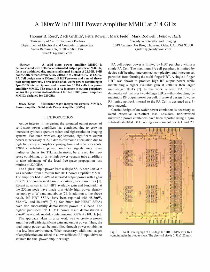
Fig. 1. An IC micrograph of a 3-Stage InP HBT SSPA with 16:1 combining in the output stage. The physical size is 2.51x2.22mm2.
combining [3]. In this work, a new 4:1 power combiner is
designed to improve the phase difference and impedance match
among the combiner’s ports.
Intermediate power amplifier stages are often required for
power amplifiers at 220GHz due to limited available RF power
from commercially available sources. Multi-stage InP power
amplifiers have been demonstrated [1, 4, 6]. The power
required from a driving stage is the input power required to
drive the next stage into compression plus losses in DC
blocking, power splitting/combining, and impedance matching.
This paper demonstrates a 2:1 amplifier stage sizing ratio that
allows full saturation of the output stage while conserving DC
power in the driving stages.
A 3-stage, 16-cell InP HBT SSPA, similar to that shown in
Fig. 1, with a total output periphery of 768x0.25μm2 is reported.
The SSPA exhibits 22.0dB of small signal gain at 214GHz and
has a –3dB point at 230GHz. At 214GHz, 180mW of saturated
output power was measured using top-surface –20ºC forced air
cooling on a full-thickness (25-mil InP) on-wafer test. At
220GHz, 157mW of saturated output power was observed. To
the author’s knowledge, the work reported here is a new state-
of-the-art for POUT achieved at these frequencies from any
semiconductor technology using on-wafer power combining.
II. 250NM INDIUM PHOSPHIDE HBT PROCESS
The reported power amplifier MMIC uses a 250nm InP HBT
technology with a ~4.5V breakdown voltage. A single HBT has
a peak bandwidth of ƒMAX = 700GHz and ƒT = 400GHz. At the
amplifier’s quiescent bias of JE = 5.5mA/μm2, ƒMAX = 590GHz
and ƒT =350GHz. The power amplifier MMIC uses common-
emitter (CE) and common-base (CB) HBTs in an AC coupled
cascode topology, with a total emitter periphery of 4-fingers x
6μm (LE = 24μm) for each device. The 4-finger CE HBT
exhibits ƒMAX = 530GHz and ƒT = 333GHz at the amplifier’s
quiescent bias. This shows that parasitics associated with the
device layout does little to decrease the available gain at
220GHz for the PA cell. The physical sizes of device footprints
are 18x7.5μm2 for CE and 6x9μm2 for CB configuration. A
more complete analysis and reporting of these cells can be
found in [7, 8].
A four-metal interconnect stack is used in MMIC fabrication.
Compact, stacked interconnect vias provide access from the top
layer of gold interconnect metal (3-μm thick) to the three lower
gold layers (each 1-μm thick). The four interconnects layers are
separated by 1-μm BCB (εr=2.7) dielectric layers. MIM
capacitors in the technology are 0.3fF/μm2 and thin-film
resistors are 50Ω/square.
III. MMIC POWER AMPLIFIER DESIGN
Amplifier circuits were simulated in ADS using an Agilent-
HBT model for the 250nm HBT technology. All interconnects,
transmission lines, MIM capacitors, probe pads, and power
splitter/combiner structures were simulated using ADS
Momentum, a 2.5-D electromagnetic simulator.
Thin film microstrip transmission lines were formed using
the lowest metal interconnect layer as ground and the upper
three metal interconnect layers for signal transmission.
Substrate-shielded, non-inverted thin-film microstrip wiring
was selected to minimize interconnect inductance between the
ground plane and the emitter terminal for the common emitter
(CE) HBT and between the ground plane and the base terminal
for the common base (CB) HBT. This is especially important
for the common base HBT, as additional inductance at the base
causes significant reduction to amplifier stability margin and
maximum stable gain. Use of a substrate-shielding ground
Fig. 2. Schematic of the cascode HBT power amplifier cell.
(a)
(b)
Fig. 2. (a) Schematic for a cascode power amplifier cell. The output is tuned as a three-port network. Compared to the previous work, the PA cell output periphery has doubled to 8x6µm. (b) A top-level schematic of the SSPA MMIC.
plane keeps signal coupling between PA cells through the 12.8
εr InP substrate small. For amplifiers with high gain,
unintentional feedback through the substrate to preceding
stages can potentially cause the amplifier to oscillate.
A single power amplifier (PA) cell is designed with a cascode
topology using two 4-finger CE HBT and two 4-finger CB HBT
as shown in Fig. 2(a). In previous work, 4-finger CB HBTs
were placed at a distance of 100μm apart. In this design,
nearest-neighbor HBT spacing increased by more than a factor
of two compared to the previous work [1] to increase the output
periphery and output power per PA cell. In order to maintain
high performance given higher power dissipation per unit area,
post-fabrication wafer thinning and heat sinking were planned.
DC bias was provided to each HBTs using quarter-wave
chokes. Bypass capacitors with resistive damping were added
to power supply buses to dampen standing waves on the power
supply revealed in simulation.
The input of the amplifier cell is single-pole impedance
matched using a high impedance transmission line and a MIM
capacitor for maximum gain to a 50Ω system Zo.
The output of the amplifier cell is terminated such that the
CB collector voltage and electron current swing along a class-
A load line within the high performance operating area of the
device. This operating area is the region of the Ic vs. Vcb curves
defined by the HBT saturation voltage, Kirk current, safe long
term operating power density, CB breakdown voltage, and the
variation of MAG/MSG with DC bias. The quiescent DC bias
is JE=5.5mA/μm2 and VCB= 1.5V. The RF output termination is
realized with a three-port RF tuning network that
simultaneously provides the electron current source of each
4x6μm2 HBTs with the load line resistance, isolates the two
HBTs from one another, and transfers RF power to the output
of the PA Cell—a 50Ω system. The tuning network uses MIM
capacitors, high impedance transmission lines, and an isolation
resistor.
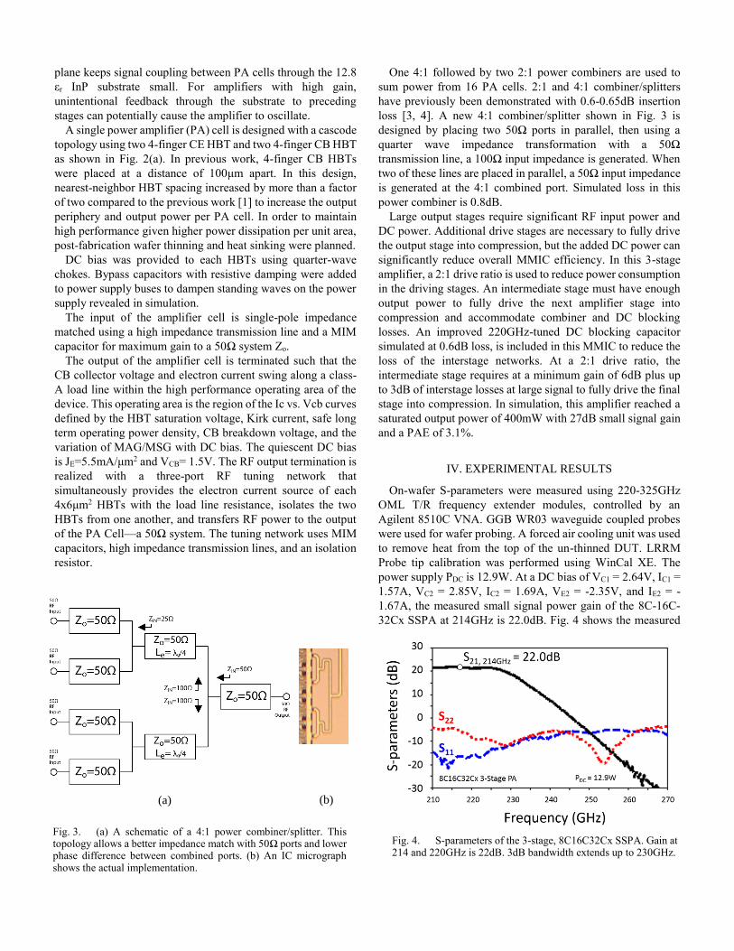
One 4:1 followed by two 2:1 power combiners are used to
sum power from 16 PA cells. 2:1 and 4:1 combiner/splitters
have previously been demonstrated with 0.6-0.65dB insertion
loss [3, 4]. A new 4:1 combiner/splitter shown in Fig. 3 is
designed by placing two 50Ω ports in parallel, then using a
quarter wave impedance transformation with a 50Ω
transmission line, a 100Ω input impedance is generated. When
two of these lines are placed in parallel, a 50Ω input impedance
is generated at the 4:1 combined port. Simulated loss in this
power combiner is 0.8dB.
Large output stages require significant RF input power and
DC power. Additional drive stages are necessary to fully drive
the output stage into compression, but the added DC power can
significantly reduce overall MMIC efficiency. In this 3-stage
amplifier, a 2:1 drive ratio is used to reduce power consumption
in the driving stages. An intermediate stage must have enough
output power to fully drive the next amplifier stage into
compression and accommodate combiner and DC blocking
losses. An improved 220GHz-tuned DC blocking capacitor
simulated at 0.6dB loss, is included in this MMIC to reduce the
loss of the interstage networks. At a 2:1 drive ratio, the
intermediate stage requires at a minimum gain of 6dB plus up
to 3dB of interstage losses at large signal to fully drive the final
stage into compression. In simulation, this amplifier reached a
saturated output power of 400mW with 27dB small signal gain
and a PAE of 3.1%.
IV. EXPERIMENTAL RESULTS
On-wafer S-parameters were measured using 220-325GHz
OML T/R frequency extender modules, controlled by an
Agilent 8510C VNA. GGB WR03 waveguide coupled probes
were used for wafer probing. A forced air cooling unit was used
to remove heat from the top of the un-thinned DUT. LRRM
Probe tip calibration was performed using WinCal XE. The
power supply PDC is 12.9W. At a DC bias of VC1 = 2.64V, IC1 =
1.57A, VC2 = 2.85V, IC2 = 1.69A, VE2 = -2.35V, and IE2 = -
1.67A, the measured small signal power gain of the 8C-16C-
32Cx SSPA at 214GHz is 22.0dB. Fig. 4 shows the measured
Fig. 3. (a) A schematic of a 4:1 power combiner/splitter. This topology allows a better impedance match with 50Ω ports and lower phase difference between combined ports. (b) An IC micrograph shows the actual implementation.
(a) (b)
Fig. 4. S-parameters of the 3-stage, 8C16C32Cx SSPA. Gain at 214 and 220GHz is 22dB. 3dB bandwidth extends up to 230GHz.
S-parameters for the amplifier. The S21 gain is greater than
19dB from below 210GHz up to 230GHz and input return loss
is greater than 10dB from below 210GHz to 231GHz.
For large signal measurements, a WR04 VDI amplifier
multiplier chain (AMC 16× multiplier) is held at a constant
power level while a voltage controlled attenuator is used to
sweep input power to the DUT at 208, 214, and 220GHz.
Output power was measured by an Erickson PM4 sub-mm
wave power meter. Forced air cooling was used for heat
removal from the full-thickness DUT. Power data was
corrected for insertion loss of the components between the
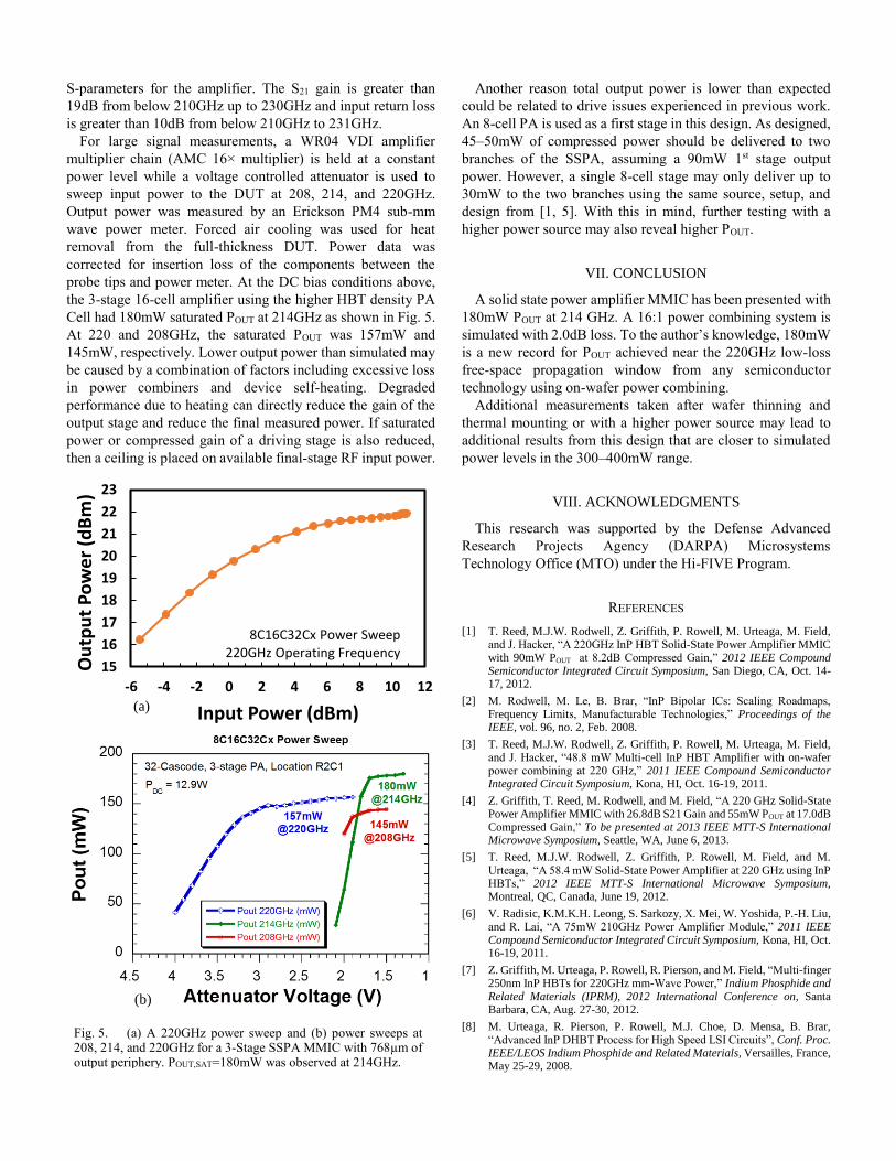
probe tips and power meter. At the DC bias conditions above,
the 3-stage 16-cell amplifier using the higher HBT density PA
Cell had 180mW saturated POUT at 214GHz as shown in Fig. 5.
At 220 and 208GHz, the saturated POUT was 157mW and
145mW, respectively. Lower output power than simulated may
be caused by a combination of factors including excessive loss
in power combiners and device self-heating. Degraded
performance due to heating can directly reduce the gain of the
output stage and reduce the final measured power. If saturated
power or compressed gain of a driving stage is also reduced,
then a ceiling is placed on available final-stage RF input power.
Another reason total output power is lower than expected
could be related to drive issues experienced in previous work.
An 8-cell PA is used as a first stage in this design. As designed,
45–50mW of compressed power should be delivered to two
branches of the SSPA, assuming a 90mW 1st stage output
power. However, a single 8-cell stage may only deliver up to
30mW to the two branches using the same source, setup, and
design from [1, 5]. With this in mind, further testing with a
higher power source may also reveal higher POUT.
VII. CONCLUSION
A solid state power amplifier MMIC has been presented with
180mW POUT at 214 GHz. A 16:1 power combining system is
simulated with 2.0dB loss. To the author’s knowledge, 180mW
is a new record for POUT achieved near the 220GHz low-loss
free-space propagation window from any semiconductor
technology using on-wafer power combining.
Additional measurements taken after wafer thinning and
thermal mounting or with a higher power source may lead to
additional results from this design that are closer to simulated
power levels in the 300–400mW range.
VIII. ACKNOWLEDGMENTS
This research was supported by the Defense Advanced
Research Projects Agency (DARPA) Microsystems
Technology Office (MTO) under the Hi-FIVE Program.
REFERENCES
[1] T. Reed, M.J.W. Rodwell, Z. Griffith, P. Rowell, M. Urteaga, M. Field, and J. Hacker, “A 220GHz InP HBT Solid-State Power Amplifier MMIC with 90mW POUT at 8.2dB Compressed Gain,” 2012 IEEE Compound Semiconductor Integrated Circuit Symposium, San Diego, CA, Oct. 14-17, 2012.
[2] M. Rodwell, M. Le, B. Brar, “InP Bipolar ICs: Scaling Roadmaps, Frequency Limits, Manufacturable Technologies,” Proceedings of the IEEE, vol. 96, no. 2, Feb. 2008.
[3] T. Reed, M.J.W. Rodwell, Z. Griffith, P. Rowell, M. Urteaga, M. Field, and J. Hacker, “48.8 mW Multi-cell InP HBT Amplifier with on-wafer power combining at 220 GHz,” 2011 IEEE Compound Semiconductor Integrated Circuit Symposium, Kona, HI, Oct. 16-19, 2011.
[4] Z. Griffith, T. Reed, M. Rodwell, and M. Field, “A 220 GHz Solid-State Power Amplifier MMIC with 26.8dB S21 Gain and 55mW POUT at 17.0dB Compressed Gain,” To be presented at 2013 IEEE MTT-S International Microwave Symposium, Seattle, WA, June 6, 2013.
[5] T. Reed, M.J.W. Rodwell, Z. Griffith, P. Rowell, M. Field, and M. Urteaga, “A 58.4 mW Solid-State Power Amplifier at 220 GHz using InP HBTs,” 2012 IEEE MTT-S International Microwave Symposium, Montreal, QC, Canada, June 19, 2012.
[6] V. Radisic, K.M.K.H. Leong, S. Sarkozy, X. Mei, W. Yoshida, P.-H. Liu, and R. Lai, “A 75mW 210GHz Power Amplifier Module,” 2011 IEEE Compound Semiconductor Integrated Circuit Symposium, Kona, HI, Oct. 16-19, 2011.
[7] Z. Griffith, M. Urteaga, P. Rowell, R. Pierson, and M. Field, “Multi-finger 250nm InP HBTs for 220GHz mm-Wave Power,” Indium Phosphide and Related Materials (IPRM), 2012 International Conference on, Santa Barbara, CA, Aug. 27-30, 2012.
[8] M. Urteaga, R. Pierson, P. Rowell, M.J. Choe, D. Mensa, B. Brar, “Advanced InP DHBT Process for High Speed LSI Circuits”, Conf. Proc. IEEE/LEOS Indium Phosphide and Related Materials, Versailles, France, May 25-29, 2008.
Fig. 5. (a) A 220GHz power sweep and (b) power sweeps at 208, 214, and 220GHz for a 3-Stage SSPA MMIC with 768µm of output periphery. POUT,SAT=180mW was observed at 214GHz.
15
16
17
18
19
20
21
22
23
-6 -4 -2 0 2 4 6 8 10 12
Ou
tpu
t P
ow
er
(dB
m)
Input Power (dBm)
8C16C32Cx Power Sweep220GHz Operating Frequency
(a)
(b)