Embed Size (px)
Citation preview

Dec. 7, 1999 1 / 31
Elec 422VLSI Design
Adaptive Noise Cancellation using theLMS Algorithm
December 7, 1999
GROUP YGROUP YYonghuiYonghui Cheng ChengDamian Damian DobricDobric
Ping TaoPing TaoShunxi Shunxi WangWang

Dec. 7, 1999 2 / 31
Elec 422VLSI DesignFunctional Description
• Adaptive Noise Cancellation DSP Circuit– Removes background noise from signals
• Application: Pilot Communication– Two signals:
• Noise + Pilot’s Speech• Noise Reference Signal in Cockpit

Dec. 7, 1999 3 / 31
Elec 422VLSI DesignFunctional Description (cont’d)
• Filter input x(k) to obtain y(k)• Error e(k) = Desired Input d(k) – y(k)
– Used to update filter frequency response• 8-tap Finite Impulse Response (FIR) Filter• LMS Algorithm
– W(k+1) = W(k) + u*2e(k)*x(k)– Fixed Step-Size u

Dec. 7, 1999 4 / 31
Elec 422VLSI DesignOverview
• Circuit Design• PLA Description• Layout• System Performance Analysis
Dec. 7, 1999 5 / 31
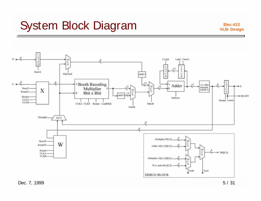
Elec 422VLSI DesignSystem Block Diagram

Dec. 7, 1999 6 / 31
Elec 422VLSI DesignSystem Timing: Error Calculation

Dec. 7, 1999 7 / 31
Elec 422VLSI DesignSystem Timing: Weight Update

Dec. 7, 1999 8 / 31
Elec 422VLSI DesignCircuit Design
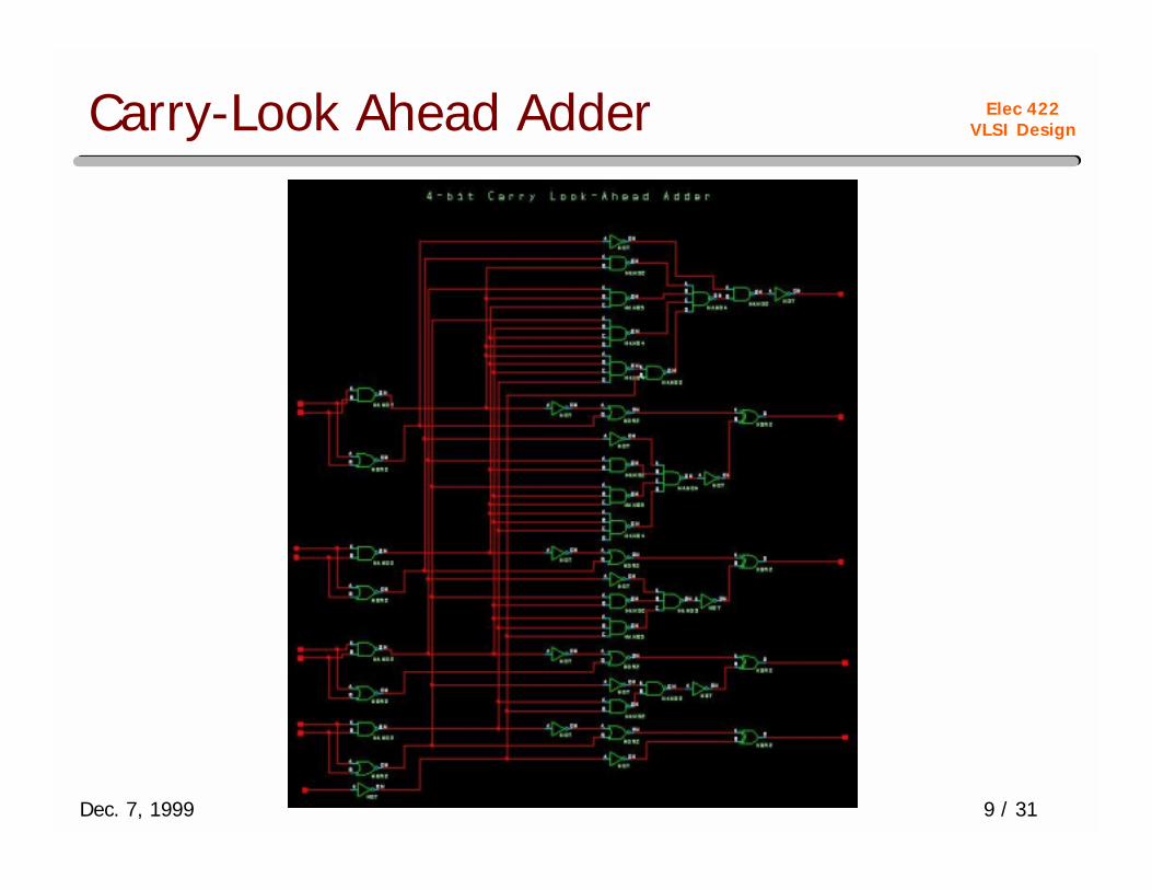
• 12-bit Carry-Look Ahead Adder• 8-bit Radix-4 Booth Recoding Multiplier• 8-bit Rotate Stack
Dec. 7, 1999 9 / 31
Elec 422VLSI DesignCarry-Look Ahead Adder

Dec. 7, 1999 10 / 31
Elec 422VLSI DesignRadix-4 Booth Recoding Multiplier

Dec. 7, 1999 11 / 31
Elec 422VLSI DesignRotate Stack

Dec. 7, 1999 12 / 31
Elec 422VLSI DesignPLA Description
• 15 states, 5 inputs, 17 outputs• 2 Phases:
– Error Computation– Filter Tap Weight Update
• 2 Counters (count to 8):– Counter to count multiplier clock cycles– Counter to count # of multiply operations
• One Iteration ~200 clock cycles

Dec. 7, 1999 13 / 31
Elec 422VLSI DesignState Diagram

Dec. 7, 1999 14 / 31
Elec 422VLSI DesignInput to Meg
-- Elec 422 Project MAIN CONTROLLER PLA
INPUTS: RESTART COUNT8 COUNT9;
OUTPUTS: STOREXD STOREW ROTATEX ROTATEW MDS MWEMMULT LOADMULT CLRCNT8 CLRCNT9 CNT8A CNT8BSUBTRACT LACCUM LERROR CLRALL CLRACCUM;
-- reset logicreset on RESTART to init(CLRALL CLRACCUM);
init: -- initial state --> clear all latchesgoto LoadXD(STOREXD LOADMULT CLRCNT8 CLRCNT9);
LoadXD: -- Load X & D inputsgoto RotateXW(ROTATEX ROTATEW CNT8A);
RotateXW: -- Rotate X & W stacksgoto StartCNT8b(CNT8B);
StartCNT8b: -- signal 8 counter w/ second control signalgoto WaitMultXWDone;
WaitMultXWDone: -- wait for the multiply of X & W to finishcase (COUNT9 COUNT8)10 => StartNextMultXW(LOADMULT LACCUM CLRCNT9);11 => StartNextMultXW(LACCUM);endcase => WaitMultXWDone;
StartNextMultXW:if COUNT8 then CalculateE(MMULT SUBTRACT)else RotateXW(ROTATEX ROTATEW CNT8A);
CalculateE:goto GetE(MMULT SUBTRACT LERROR);
GetE:goto WaitBeforeMult; -- CLKB2 happens on EVEN cycles
WaitBeforeMult:goto StartMultXE(MWE LOADMULT CLRCNT8 CLRCNT9CLRACCUM);
StartMultXE:goto GetWAdd(ROTATEX ROTATEW MDS MMULT CNT8A);
GetWAdd:goto StartCNT8b2(MDS MMULT CNT8B LACCUM);
StartCNT8b2:goto WaitMultXEDone(MDS);
WaitMultXEDone:case (COUNT9 COUNT8)10 => StartNextMultXE(MDS MWE STOREW LOADMULTCLRCNT9);11 => StartNextMultXE(MDS STOREW ROTATEX);endcase => WaitMultXEDone(MDS);
StartNextMultXE:if COUNT8 then WaitBeforeMult2 -- CLKB2 happens on EVENcycleselse StartMultXE(CLRACCUM);
WaitBeforeMult2:goto init(CLRALL CLRACCUM);

Dec. 7, 1999 15 / 31
Elec 422VLSI DesignLayout
• Cell Hierarchy• Plots of Low-Level Cells• Floorplan• Full plot of Chip

Dec. 7, 1999 16 / 31
Elec 422VLSI DesignCell Hierarchy

Dec. 7, 1999 17 / 31
Elec 422VLSI DesignXOR Gate Cell

Dec. 7, 1999 18 / 31
Elec 422VLSI Design5-Input NAND Gate Cell
Dec. 7, 1999 19 / 31
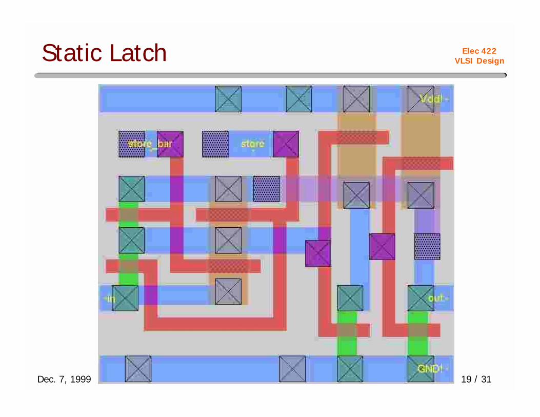
Elec 422VLSI DesignStatic Latch

Dec. 7, 1999 20 / 31
Elec 422VLSI DesignClearable Static Latch

Dec. 7, 1999 21 / 31
Elec 422VLSI Design4-bit Carry-Look Ahead Adder

Dec. 7, 1999 22 / 31
Elec 422VLSI Design12-bit Carry-Look Ahead Adder

Dec. 7, 1999 23 / 31
Elec 422VLSI Design8-bit Radix-4 Booth Recoding Mult.

Dec. 7, 1999 24 / 31
Elec 422VLSI Design8x8-bit Rotate Stack
Dec. 7, 1999 25 / 31
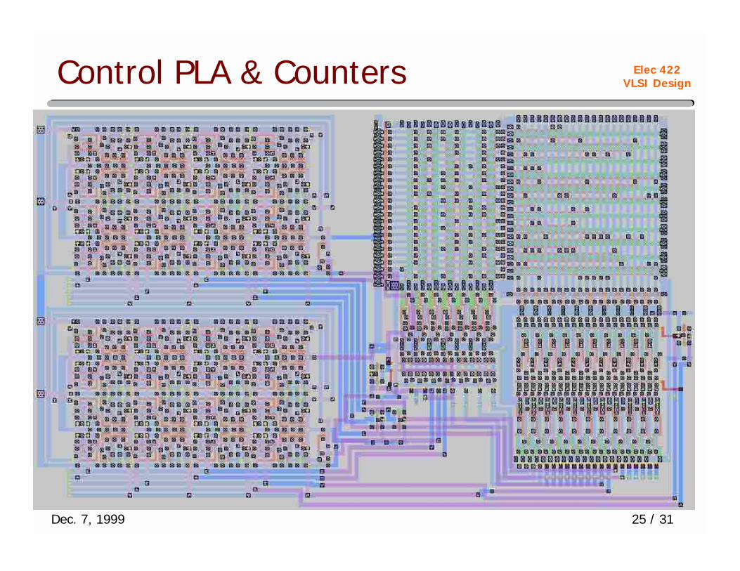
Elec 422VLSI DesignControl PLA & Counters
Dec. 7, 1999 26 / 31
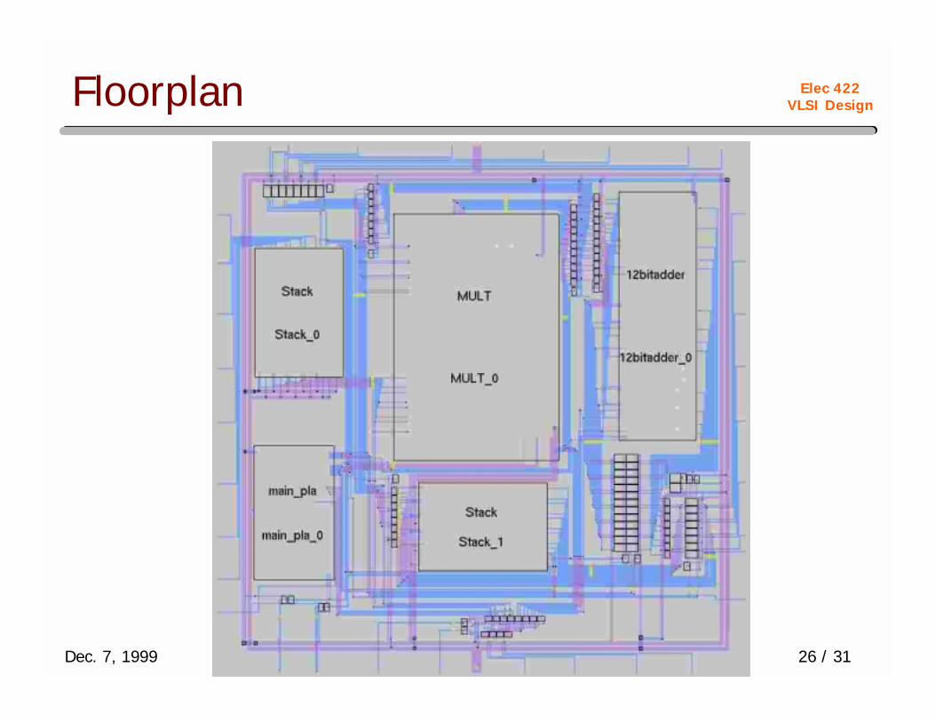
Elec 422VLSI DesignFloorplan
Dec. 7, 1999 27 / 31
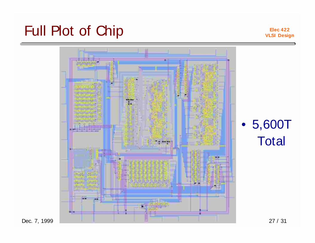
Elec 422VLSI DesignFull Plot of Chip
• 5,600T Total
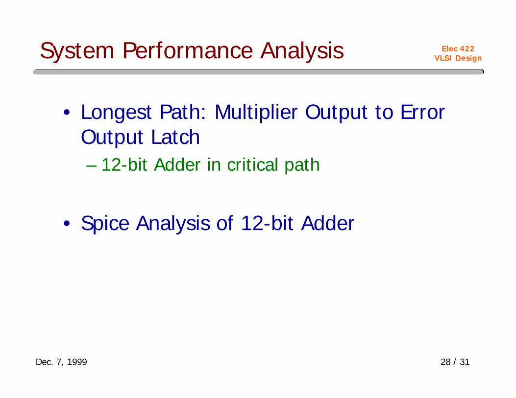
Dec. 7, 1999 28 / 31
Elec 422VLSI DesignSystem Performance Analysis
• Longest Path: Multiplier Output to ErrorOutput Latch– 12-bit Adder in critical path
• Spice Analysis of 12-bit Adder

Dec. 7, 1999 29 / 31
Elec 422VLSI DesignSpice Analysis (Rise Time)
• Rise Time ~23.5 ns

Dec. 7, 1999 30 / 31
Elec 422VLSI DesignSpice Analysis (Fall Time)
• Fall Time ~22 ns

Dec. 7, 1999 31 / 31
Elec 422VLSI DesignSummary of System Performance
• 12-bit Adder Worst Case Delay: ~25 ns
• Maximum Clock Speed: ~42.6 MHz


![LMS - download.mastersolution.agdownload.mastersolution.ag/media/LMS/MASTERSOLUTION_LMS_FLYER.pdf · Lern Management System [LMS] – individuelle Lernplattform, Benutzerverwaltung,](https://img.dokumen.tips/doc/110x75/5e1d0d435c6bc20e04570e9c/lms-lern-management-system-lms-a-individuelle-lernplattform-benutzerverwaltung.jpg)