Embed Size (px)
Citation preview

Debugging Timing Problems with a Logic AnalyzerApplication Note
IntroductionIn today’s digital world, embedded systems are more complex than ever. With the use of faster speeds, lower power devices and more powerful logic, they are becoming increasingly sensitive to signal integrity issues. While at the same time, the powerful and fast technology that enables these gains is even more likely to create signal integrity problems.
During the debug and validation process, the majority of digital faults can be traced back to signal integrity issues. In the ideal world, all signals would be unimpaired. Analog signals would have clean rises and falls with no jitter. Digital signals would have clean, fast transitions; stable, valid logic levels; accurate placement in time; and would be free of transients. However, getting close to this ideal is becoming more difficult as data speeds increase.

Application Note
www.tektronix.com/la2
At fast clock frequencies and fast edge rates, every design detail becomes important. A host of variables can affect signal integrity: signal path design, the circuit board stack-up, transmission line effects and power distribution. Given all these variables, it is inevitable there will be signal integrity issues to debug in the lab.
When these problems do come up, they are likely to appear as problems in the digital domain. That is, the binary signals on a bus or a device output will have incorrect values. The errors may appear in the waveform or timing view on a logic analyzer or they may show up at the state or even protocol level. Problems in the digital domain are usually timing related. Bus contentions, setup and hold violations, metastability, and race conditions are examples of problems in the digital domain. Each of these can cause erratic signal behavior on a bus or device output.
Problems in the analog domain such as low-amplitude signals, slow or fast transition times, glitches, crosstalk, and noise usually have their origins in the design of the circuit board or signal termination. Not surprisingly, there is a high degree of interaction and interdependence between digital and analog signal integrity issues. For example, a slow rise time on an input can cause the output pulse to be delayed which could in turn cause bus contention in the digital environment.
This application note will discuss how to solve these timing related issues by using common logic analyzer features and capabilities to quickly and easily get to the root of your design problem.
Probing ConsiderationsHaving good probing points throughout your design is critical to successfully troubleshooting problems. With good access to your signals, it is possible to correlate signal timing from different places, view traffic on buses, and analyze the hardware and software interface. Probing is key to accessing the signals, and signal access is the first step in locating the root cause of a problem.
Once test points have been decided, the next step is to identify which probes to use. The fundamental rule is that any probe needs to accurately transmit signals from the board to the acquisition system input. A logic analyzer’s probing scheme plays a crucial role in helping to find many of the problems in your system. In most embedded systems, a dedicated test point is usually the most practical way to measure signals with a logic analyzer – especially if you are trying to capture a large number of signals, such as a 32-bit address/data bus. One option is to use square pins on the board and a general purpose, flying leadset type of logic analyzer probe. This does provide a way of connecting the logic analyzer to the system, but there are issues. Most importantly, performance will be lower than other probing options because of the added loading of the square pins. This loading will always be present as long as the probe is connected, and will have an effect on the board’s performance even when the logic analyzer is not connected.
Figure 1. Example of different probe points on an embedded system design.
PCI Bus
Custom I/O
Local Bus
µP
PCIBridgeChip
SystemBus
SDRAM
Flash ROM
= Probe PointsP
P
P
P
P
P
PCI-to-SystemBridge
FPGA PCIDevice 1 Ethernet

www.tektronix.com/la 3
Debugging Timing Problems with a Logic Analyzer
Another choice is to mount a Mictor connector on the board. These compact, high-density connectors provide a convenient connection point to the logic analyzer. Again, they provide fast, positive connections for large groups of signals but still will have an impact on high-speed signal operation.
Even higher-density options, such as D-Max™ probing technology, have emerged to provide an alternative to conventional Mictor probes. These probes require no connectors on the board. Instead, they mate directly to land pads on the board and are held in place by small retention posts. These probes address lead inductance and reduce capacitive loading to about 0.5 pF. They come in single-ended and differential versions. These types of probe offer the highest performance as well as the highest-density.
In addition to the physical connection, it is critical to consider probe performance since probes with high total capacitance can change how your system performs and introduce (or hide) timing problems. In high-speed systems, excessive probe capacitance can potentially prevent the system under test (SUT) from working! It is always critical to choose a probe with the lowest possible total capacitance. Total capacitance means the capacitance presented by the probe to the SUT which is the sum of parasitic tip capacitance and the attenuator capacitance.
Probe capacitance tends to roll-off the edges of signal transitions, as shown in Figure 3. This roll-off slows down the edge transition by an amount of time represented as tΔ in Figure 3. Why is this important? Because a slower edge crosses the logic threshold of the circuit later, introducing timing errors in the SUT. This is a problem that becomes more severe as clock rates increase. Higher probe capacitance can distort the timing of the SUT making the accuracy of edge-to-edge measurements in the nanosecond and sub-nanosecond range very questionable.
Tektronix offers a range of probes that provide square pin connections, as well as Mictor and D-Max connections. In all cases, these probes provide outstanding performance in terms of capacitance and are always specified for the total capacitance that the probe presents to the SUT. This provides for a range of reliable, trustworthy probes that meet the physical and electrical requirements of virtually all embedded systems designs.
Figure 2. D-Max connectorless logic analyzer probe.
Figure 3. The impedance of the logic analyzer’s probe can affect signal rise times and measured timing relationships.

Application Note
www.tektronix.com/la4
Logic Analyzer Performance Terms and ConsiderationsThe logic analyzer’s performance and feature set play a key role in determining how long it will take to find the root cause of a problem. To understand how to select the right logic analyzer for your need, the purpose of the logic analyzer needs to be first understood.
The logic analyzer’s most basic mission is to produce a timing diagram based on the data it has acquired. If the SUT is functioning correctly and the acquisition is properly set up, the logic analyzer’s timing display will be virtually identical to the timing diagram from the design simulator or data book. But that depends on the resolution of the logic analyzer—in effect, its sample rate. Timing acquisition is asynchronous; that is, the sample clock is free-running relative to the input signal. The higher the sample rate, the more likely it is that a sample will accurately detect the timing of an event such as a glitch. For example, a Tektronix TLA Series logic analyzer with a sample frequency of 2 GHz provides 500 ps resolution. Therefore, the timing display reflects edge placements within 500 ps of the actual edge.
For analysis of faster signals, logic analyzers typically provide a higher resolution acquisition mode that accumulates additional samples around the trigger point. The TLA Series logic analyzer offers up to 50 GHz sampling on all channels with its MagniVu™ high-resolution acquisition mode. Additional capabilities include adjustable MagniVu sample rates, movable trigger positions, and a separate MagniVu trigger action that can be triggered independent of the main trigger. All of these features provide the flexibility to capture a wide variety of timing problems.
With any logic analyzer or in fact any measurement instrument, you need to look beyond just the instrument’s specifications. It’s important to consider how all the features and performance attributes play together to improve the overall performance of the instrument. For the logic analyzer, it is important to understand the relationship between the higher resolution sampler and the standard sampling mode. How these two samplers are implemented within the logic analyzer will greatly affect the accuracy of the data on display.
There are two common architectures used in logic analyzers today. The first approach uses two independent and separate samplers (see Figure 4), one for the high-resolution acquisition and the other for standard acquisition mode. Since this approach relies on two different time bases, it naturally leads to greater uncertainly between the data because there will be skew between these two different time bases. With skew between the two different datasets, it becomes difficult to make accurate timing measurements between channels that are on different datasets because of the built-in uncertainty.
Figure 4. Example of a logic analyzer architecture using two independent samplers.
4GHzSampler
500ps DeepMemory Timing
250ps HighSpeed Timing
www.tektronix.com/la 5
Debugging Timing Problems with a Logic Analyzer
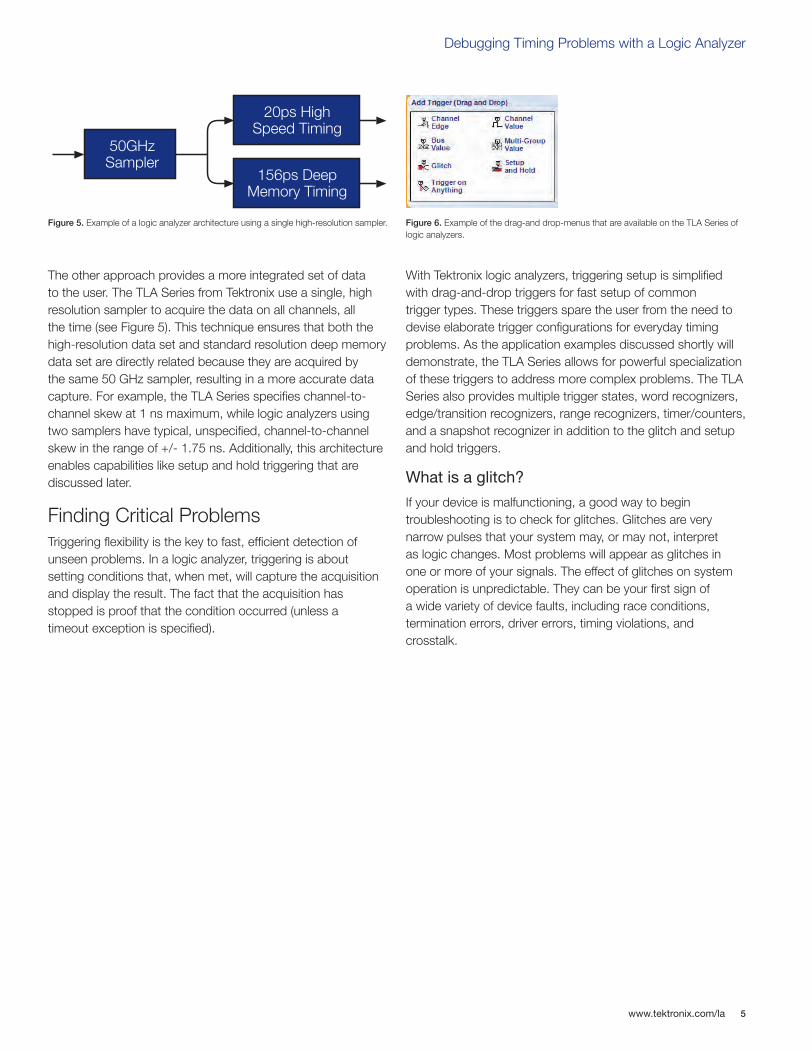
The other approach provides a more integrated set of data to the user. The TLA Series from Tektronix use a single, high resolution sampler to acquire the data on all channels, all the time (see Figure 5). This technique ensures that both the high-resolution data set and standard resolution deep memory data set are directly related because they are acquired by the same 50 GHz sampler, resulting in a more accurate data capture. For example, the TLA Series specifies channel-to-channel skew at 1 ns maximum, while logic analyzers using two samplers have typical, unspecified, channel-to-channel skew in the range of +/- 1.75 ns. Additionally, this architecture enables capabilities like setup and hold triggering that are discussed later.
Finding Critical ProblemsTriggering flexibility is the key to fast, efficient detection of unseen problems. In a logic analyzer, triggering is about setting conditions that, when met, will capture the acquisition and display the result. The fact that the acquisition has stopped is proof that the condition occurred (unless a timeout exception is specified).
With Tektronix logic analyzers, triggering setup is simplified with drag-and-drop triggers for fast setup of common trigger types. These triggers spare the user from the need to devise elaborate trigger configurations for everyday timing problems. As the application examples discussed shortly will demonstrate, the TLA Series allows for powerful specialization of these triggers to address more complex problems. The TLA Series also provides multiple trigger states, word recognizers, edge/transition recognizers, range recognizers, timer/counters, and a snapshot recognizer in addition to the glitch and setup and hold triggers.
What is a glitch?
If your device is malfunctioning, a good way to begin troubleshooting is to check for glitches. Glitches are very narrow pulses that your system may, or may not, interpret as logic changes. Most problems will appear as glitches in one or more of your signals. The effect of glitches on system operation is unpredictable. They can be your first sign of a wide variety of device faults, including race conditions, termination errors, driver errors, timing violations, and crosstalk.
Figure 5. Example of a logic analyzer architecture using a single high-resolution sampler.
50GHzSampler
20ps HighSpeed Timing
156ps DeepMemory Timing
Figure 6. Example of the drag-and drop-menus that are available on the TLA Series of logic analyzers.

Application Note
www.tektronix.com/la6
Locating the glitch
Since the problems that glitches cause are often intermittent, they can be very hard to resolve. A good approach is to combine classic top/down troubleshooting with the specific advantages of your test instruments. Start wide, with a macro view of device operation, and then begin focusing in on specific problems.
One of the most powerful and easy to use glitch hunting tools, when no more than 4 channels needs to be simultaneously investigated, is a Digital Phosphor Oscilloscope (DPO). A DPO provides unmatched insight into signal behavior by displaying, storing and analyzing complex signals in real-time using three dimensions of signal information: amplitude, time and distribution of amplitude over time. With its continuous waveform capture rate of up to 300,000 waveforms per second, it is the industry’s most efficient tool to capture elusive signal glitches and intermittent events and is ideal for digital debug. A DPO is also extremely easy to use, and in an instant, you’ll have a real-time visual overview of what’s really happening in your signal. You can then use the oscilloscope’s
advanced triggering capabilities to further characterize the problem. All Tektronix oscilloscopes offer extensive trigger possibilities that allow you to quickly and easily trigger on the event of interest and further analyze it.
If you need to perform glitch hunting on more than 4 channels, your Tektronix logic analyzer enables glitch triggering on buses that are hundreds of signals wide. The logic analyzer checks every signal for glitches. Red bars on the bus timing diagrams show glitch locations for further analysis. You can then use a Tektronix oscilloscope to help further characterize the problem by revealing exactly what the glitch looks like in the analog domain. Using the iView™ measurements on the TLA Series logic analyzers, you can combine your logic analyzer and your oscilloscope into a single system and progressively “zoom in” on the problem. Using the top/down methodology and stepping through the debugging process to find glitches and troubleshoot the problem is the fastest and easiest way to solve the problem. In the following four steps, this process will be used to identify two different glitches and their likely source.
Figure 8. An advanced and wide selection of oscilloscope triggering capabilities enables you to quickly and easily capture different type of signals on a Tektronix oscilloscope. The DPO7000 Series is shown here.
Figure 7. Tektronix DPO7000 Series Digital Phosphor Oscilloscope (DPO) maximizes the probability of capturing elusive glitches and other infrequent events.

www.tektronix.com/la 7
Debugging Timing Problems with a Logic Analyzer
Figure 9. Sample ticks. Control bus and Address bus showing red glitch flags.
Step I: Examine the bus
The first step is to focus on what works and look globally for faults. Your logic analyzer’s bus timing waveform will flag any glitches that occur. When it comes to looking for intermittent effects, such as glitches, a logic analyzer with a long record length is necessary. The TLA Series offers up to 512 Mb of deep timing capability.
The logic analyzer’s bus timing waveform can examine all the signal lines of the bus at once. If the logic analyzer detects a glitch on any of the lines, it will flag the bus and the time location. In Figure 9, the top waveform is Sample, which shows the sample ticks that represent the logic analyzer’s deep timing sampling rate of up to 2 GHz (500 ps). The next two lines are the bus waveforms – the 4-bit Control bus and the 8-bit Address bus. The red glitch flags that appear on both bus waveforms signify that there was more than one transition between the sample points at those locations.
Step II: Examine the lines
The next step is to focus on where the problems are. The logic analyzer’s timing signal waveform can display the individual lines of the bus and flag where glitches occur. In Figure 10, the logic analyzer has expanded the Control bus into its four individual signals and the Address bus into its eight individual signals. The red glitch flags from the bus waveform in Figure 9 are now shown as glitch flags on signal lines Control (3) and Control (0), and as two glitches on the Address (0) signal line.
Figure 10. 4-bit Control bus and 8-bit Address bus expanded showing red glitch flags on individual signals.

Application Note
www.tektronix.com/la8
Figure 12. Control (0) and Address (0) lines with MagniVu traces showing glitches caused by crosstalk.
Step III: Take a closer look
To examine the faults in fine detail, the high-resolution timing view is used. It will show how these faults relate to other events or faults. In addition to deep timing, the TLA Series has high-resolution MagniVu 20 ps (50 GHz) timing capability that runs simultaneously with the deep timing capability. MagniVu waveforms can display all channels in high-resolution up to a 16 Kb memory depth. It is like having two logic analyzers in one: a deep timing logic analyzer and a high-resolution timing logic analyzer, both using the same probes.
In this example, it appears there may be two different problems causing glitches. To examine the Control (3) signal line further, the MagniVu trace for the Control (3) signal is displayed. Figure 11 shows that because of its higher resolution, the MagniVu waveform reveals that the glitch only appears at the end of a digital pulse – not at the beginning of the pulse, and not by itself. This is an important clue to the cause of the fault.
Now, the MagniVu high-resolution timing is used to examine the two remaining flagged lines, Control (0) and Address (0). Figure 12 shows that since the MagniVu waveforms are examining the signals at a much higher resolution, 20 ps, they are able to discern far narrower glitches on the two lines. Note that the glitch and a pulse occur at the same time on both signal lines. That often indicates crosstalk between the two signals. To be sure, it’s necessary to take a different kind of close-up look at the signals. Proceeding to Step IV will reveal more about this.
Figure 11. MagnuiVu waveform of Control (3) showing glitch.
www.tektronix.com/la 9
Debugging Timing Problems with a Logic Analyzer
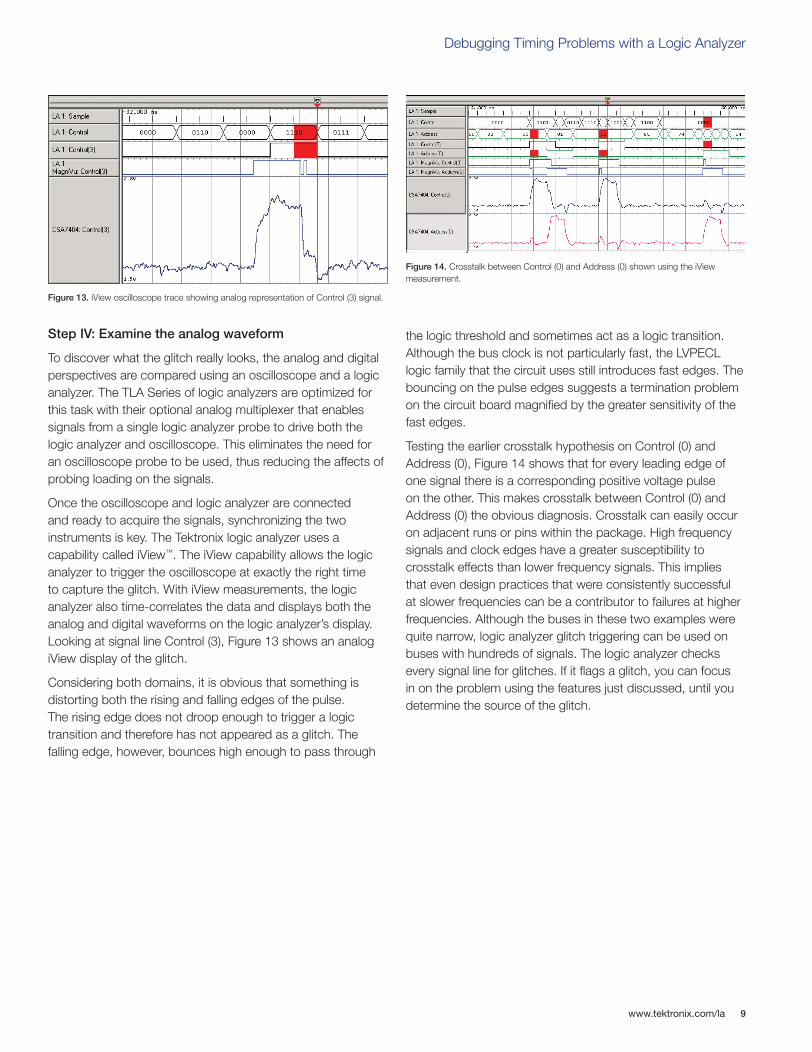
Figure 13. iView oscilloscope trace showing analog representation of Control (3) signal.
Figure 14. Crosstalk between Control (0) and Address (0) shown using the iView measurement.
Step IV: Examine the analog waveform
To discover what the glitch really looks, the analog and digital perspectives are compared using an oscilloscope and a logic analyzer. The TLA Series of logic analyzers are optimized for this task with their optional analog multiplexer that enables signals from a single logic analyzer probe to drive both the logic analyzer and oscilloscope. This eliminates the need for an oscilloscope probe to be used, thus reducing the affects of probing loading on the signals.
Once the oscilloscope and logic analyzer are connected and ready to acquire the signals, synchronizing the two instruments is key. The Tektronix logic analyzer uses a capability called iView™. The iView capability allows the logic analyzer to trigger the oscilloscope at exactly the right time to capture the glitch. With iView measurements, the logic analyzer also time-correlates the data and displays both the analog and digital waveforms on the logic analyzer’s display. Looking at signal line Control (3), Figure 13 shows an analog iView display of the glitch.
Considering both domains, it is obvious that something is distorting both the rising and falling edges of the pulse. The rising edge does not droop enough to trigger a logic transition and therefore has not appeared as a glitch. The falling edge, however, bounces high enough to pass through
the logic threshold and sometimes act as a logic transition. Although the bus clock is not particularly fast, the LVPECL logic family that the circuit uses still introduces fast edges. The bouncing on the pulse edges suggests a termination problem on the circuit board magnified by the greater sensitivity of the fast edges.
Testing the earlier crosstalk hypothesis on Control (0) and Address (0), Figure 14 shows that for every leading edge of one signal there is a corresponding positive voltage pulse on the other. This makes crosstalk between Control (0) and Address (0) the obvious diagnosis. Crosstalk can easily occur on adjacent runs or pins within the package. High frequency signals and clock edges have a greater susceptibility to crosstalk effects than lower frequency signals. This implies that even design practices that were consistently successful at slower frequencies can be a contributor to failures at higher frequencies. Although the buses in these two examples were quite narrow, logic analyzer glitch triggering can be used on buses with hundreds of signals. The logic analyzer checks every signal line for glitches. If it flags a glitch, you can focus in on the problem using the features just discussed, until you determine the source of the glitch.

Application Note
www.tektronix.com/la10
Looking for Setup and Hold ViolationsSetup and hold compliance is one of the most crucial timing parameters in a digital system. The traditional approach is to verify setup and hold timing using two oscilloscope channels and probing the clock and data lines one-by-one. This becomes tedious and time consuming when there are numerous signal traces running on the circuit. However, a logic analyzer can scan entire system buses to trigger on and display setup and hold violations automatically. Only setup and hold triggering lets you deterministically trap a single violation of setup and hold time that would almost certainly be missed by using other trigger modes. This trigger mode makes it easy to capture specific signal quality and timing details when a synchronous data signal fails to meet setup and hold specifications.
To simplify the process, test points should be created during the design phase that will allow the logic analyzer’s probe to easily access the clock and target signals. Logic analyzers that are able to clock system signals in timing mode and state mode simultaneously are critical for this task. State mode enables a logic analyzer to trigger on setup and hold violations, while a high-resolution timing mode enables the user to measure the violation. Following is an example of verifying setup and hold compliance using a Tektronix TLA Series logic analyzer.
Step I: Choose the logic analyzer’s clocking mode
The first step is to choose the clocking mode of the logic analyzer. In this case, synchronous mode will be used.
Performance logic analyzers have two ways to clock target signals: asynchronous mode and synchronous mode. In the asynchronous mode, also called timing mode, the logic analyzer samples the signals of the system under test periodically by using an internal clock. The user can adjust the sample rate to change the timing resolution.
In the synchronous mode, also called state mode, the logic analyzer samples acquired signals according to an external clock, which is typically synchronized with device signals. In this mode, logic analyzer users can see waveform states only when they are valid. To capture setup and hold violations, a comparison between the waveform edge timing relationship of the clock and target signals must be made. Therefore, synchronous mode must be used to capture setup and hold violations.
Step II: Set up triggering
The next step is to drag and drop the “Setup and Hold” trigger option onto the target buses and define bus setup and hold specifications (see Figures 16 and 17). In this example, the data bus has a specification of 1 ns setup time and 500 ps hold time.
Figure 16. Selecting the “Setup and Hold” trigger option.
Figure 15. Changing the clocking mode.
Figure 17. Specifying setup and hold times.

www.tektronix.com/la 11
Debugging Timing Problems with a Logic Analyzer
Step III: Capture setup and hold violations
After defining the trigger condition, you simply press the “Run” button to begin a new acquisition. The logic analyzer automatically examines thousands of active waveform edges
in accordance with the clock edge. As soon as the logic analyzer identifies a setup and hold violation, it will trigger and place red flags on the screen to display the violation areas (see Figure 19).
This process enables you to identify problem areas quickly. Plus, you can also use the logic analyzer’s automated measurements to determine how many violations are in the system’s buses (see Figure 18).
Figure 19. A red flag indicates a violation.
Figure 18. Automated measurements identify the violation counts and rates.
Application Note
www.tektronix.com/la12
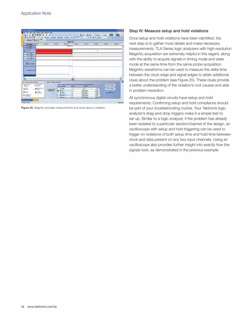
Step IV: Measure setup and hold violations
Once setup and hold violations have been identified, the next step is to gather more details and make necessary measurements. TLA Series logic analyzers with high-resolution MagniVu acquisition are extremely helpful in this regard, along with the ability to acquire signals in timing mode and state mode at the same time from the same probe acquisition. MagniVu waveforms can be used to measure the delta time between the clock edge and signal edges to attain additional clues about the problem (see Figure 20). These clues provide a better understanding of the violation’s root causes and aids in problem resolution.
All synchronous digital circuits have setup and hold requirements. Confirming setup and hold compliance should be part of your troubleshooting routine. Your Tektronix logic analyzer’s drag-and-drop triggers make it a simple test to set up. Similar to a logic analyzer, if the problem has already been isolated to a particular section/channel of the design, an oscilloscope with setup and hold triggering can be used to trigger on violations of both setup time and hold time between clock and data present on any two input channels. Using an oscilloscope also provides further insight into exactly how the signals look, as demonstrated in the previous example.
Figure 20. MagniVu provides measurements and clues about a violation.

www.tektronix.com/la 13
Debugging Timing Problems with a Logic Analyzer
Figure 21. The wide range of zero latency time violation triggers available with the TLA Series.
Figure 22. A very useful minimum pulse width violation trigger setup.
Timing Errors – Time Between Edges or EventsWhen a logic analyzer has an internal timer that can be tested by the logic analyzer’s trigger state machine, a wide range of timing violation triggering setups are possible. Testable timers allow triggering on pulse width violations (too narrow or too wide) or triggering when any two events violate your timing parameters. As circuits get faster, it is important that the trigger timers be as fast as possible.
Trigger timers sometimes exhibit latency between when they are started and when they can be checked. For example, the time between the rising edge of a pulse and the start of the timer. The timer will stop when it sees a falling edge, and then verify the time elapsed is either higher or lower than the target value set for the comparison test. Timer latency will determine the minimum time value that can be tested in the comparison. If a timer has a latency of 60 ns, it can’t be used to find any fault that is less than 60 ns in width. Triggering on pulses that are narrower than 60 ns, triggering when a data acknowledge comes too soon (under 60 ns) to be seen by the transmitting circuit, or triggering on any minimum time violation that is faster than 60 ns is simply impossible.
All Tektronix TLA Series logic analyzers have zero latency trigger timers. Triggering on pulse width violations down to 200 ps in width is possible with the TLA Series logic analyzers.

Application Note
www.tektronix.com/la14
SummaryTiming problems are commonplace in many embedded designs and troubleshooting them can be a time consuming task. The right logic analyzer will simplify and speed this process.
When looking at just specifications, many logic analyzers appear to have similar performance. To ensure that the logic analyzer you rely on is able to acquire your signal accurately and find problems quickly, you must look beyond specifications and consider the logic analyzer’s architecture and features. Probes with low total capacitance will capture your signals with minimum disruption to signal quality. A single sampling architecture will ensure data capture is accurate. Capabilities like Glitch Capture and Display, and Setup and Hold Violation Triggering, will dramatically shorten the time it takes to find timing errors.
With up to 512 Mb deep memory and 20 ps timing resolution with MagniVu high-resolution timing, plus powerful features like Glitch Capture and Display and Analog Multiplexing, the TLA Series provides the performance and tools you need to capture even elusive timing problems on today’s fast designs.
Single Probing Solution for both Analog and Digital Analysis
Correlating the analog and digital domains has traditionally required connecting both your oscilloscope and logic analyzer to the system under test. The TLA7ACx Series and TLA7Bxx Series of logic analyzer modules from Tektronix offer a unique solution. A built-in analog multiplexer enables the oscilloscope and logic analyzer to share the same logic analyzer probe, providing simultaneous state, high-speed timing and analog analysis to pinpoint elusive faults without double probing.
Any one of the 136 channel inputs to the logic analyzer can be routed directly to the oscilloscope for simultaneous analog measurements. The output from the logic analyzer to the oscilloscope is always live and four channels can be sent to the oscilloscope at any one time. With an analog bandwidth of up to 3 GHz, this capability is a powerful tool for troubleshooting and finding the root cause of timing errors that are found in many of today’s complex embedded designs.
34
3 GHzAnalog
Mux
CH 1
CH 2
CH 3
CH 4
CH 1
Analog Out
Logic Analyzer Logic Analyzer
Analog In
CH 2
CH 3
CH 4
34
34
34
OscilloscopeOscilloscope
Figure 23. Built-in analog multiplexer enables the oscilloscope and logic analyzer to share the same logic analyzer probe, providing simultaneous state, timing and analog analysis.
www.tektronix.com/la 15
Debugging Timing Problems with a Logic Analyzer
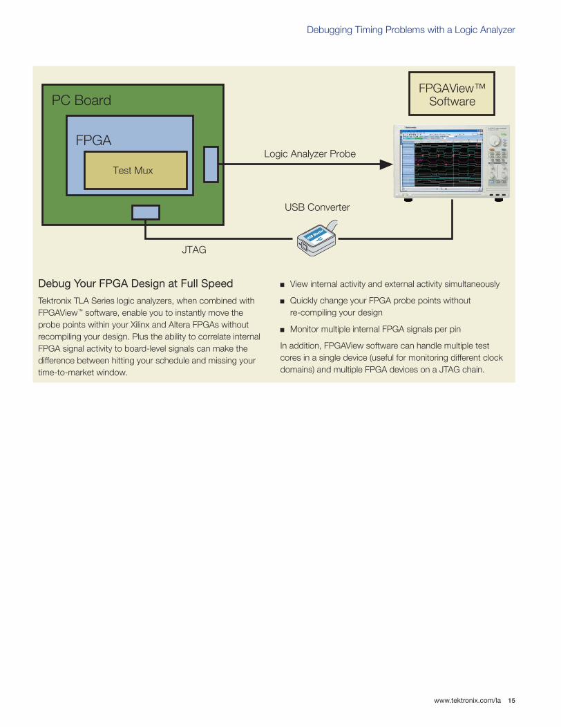
Debug Your FPGA Design at Full Speed
Tektronix TLA Series logic analyzers, when combined with FPGAView™ software, enable you to instantly move the probe points within your Xilinx and Altera FPGAs without recompiling your design. Plus the ability to correlate internal FPGA signal activity to board-level signals can make the difference between hitting your schedule and missing your time-to-market window.
View internal activity and external activity simultaneously
Quickly change your FPGA probe points without re-compiling your design
Monitor multiple internal FPGA signals per pin
In addition, FPGAView software can handle multiple test cores in a single device (useful for monitoring different clock domains) and multiple FPGA devices on a JTAG chain.
PC Board
FPGA
Test Mux
Logic Analyzer Probe
USB Converter
JTAG
FPGAView™Software

Contact Tektronix:ASEAN / Australasia (65) 6356 3900
Austria +41 52 675 3777
Balkans, Israel, South Africa and other ISE Countries +41 52 675 3777
Belgium 07 81 60166
Brazil +55 (11) 40669400
Canada 1 (800) 661-5625
Central East Europe, Ukraine and the Baltics +41 52 675 3777
Central Europe & Greece +41 52 675 3777
Denmark +45 80 88 1401
Finland +41 52 675 3777
France +33 (0) 1 69 86 81 81
Germany +49 (221) 94 77 400
Hong Kong (852) 2585-6688
India (91) 80-42922600
Italy +39 (02) 25086 1
Japan 81 (3) 6714-3010
Luxembourg +44 (0) 1344 392400
Mexico, Central/South America & Caribbean 52 (55) 54247900
Middle East, Asia and North Africa +41 52 675 3777
The Netherlands 090 02 021797
Norway 800 16098
People’s Republic of China 86 (10) 6235 1230
Poland +41 52 675 3777
Portugal 80 08 12370
Republic of Korea 82 (2) 6917-5000
Russia & CIS +7 (495) 7484900
South Africa +27 11 206 8360
Spain (+34) 901 988 054
Sweden 020 08 80371
Switzerland +41 52 675 3777
Taiwan 886 (2) 2722-9622
United Kingdom & Ireland +44 (0) 1344 392400
USA 1 (800) 426-2200
For other areas contact Tektronix, Inc. at: 1 (503) 627-7111
Updated 30 October 2008
For Further InformationTektronix maintains a comprehensive, constantly expanding collection of application notes, technical briefs and other resources to help engineers working on the cutting edge of technology. Please visit www.tektronix.com
Copyright © 2009, Tektronix. All rights reserved. Tektronix products are covered by U.S. and foreign patents, issued and pending. Information in this publication supersedes that in all previously published material. Specification and price change privileges reserved. TEKTRONIX and TEK are registered trademarks of Tektronix, Inc. All other trade names referenced are the service marks, trademarks or registered trademarks of their respective companies. 05/09 EA/WOW 52W-23621-0