Embed Size (px)
Citation preview

TimingAnalyzer Guide
Timing Analyzer Guide — 3.1i
Introduction
Getting Started
Timing Analysis
Using the Timing Analyzer
Glossary
Printed in U.S.A.

Timing Analyzer Guide

Timing Analyzer Guide
R
The Xilinx logo shown above is a registered trademark of Xilinx, Inc.
ASYL, FPGA Architect, FPGA Foundry, NeoCAD, NeoCAD EPIC, NeoCAD PRISM, NeoROUTE, Timing Wizard,TRACE, XACT, XILINX, XC2064, XC3090, XC4005, XC5210, and XC-DS501 are registered trademarks of Xilinx,Inc.
The shadow X shown above is a trademark of Xilinx, Inc.
All XC-prefix product designations, A.K.A Speed, Alliance Series, AllianceCORE, BITA, CLC, Configurable LogicCell, CoolRunner, CORE Generator, CoreLINX, Dual Block, EZTag, FastCLK, FastCONNECT, FastFLASH,FastMap, Fast Zero Power, Foundation, HardWire, IRL, LCA, LogiBLOX, Logic Cell, LogiCORE, LogicProfessor,MicroVia, MultiLINX, PLUSASM, PowerGuide, PowerMaze, QPro, RealPCI, RealPCI 64/66, SelectI/O,SelectRAM, SelectRAM+, Silicon Xpresso, Smartguide, Smart-IP, SmartSearch, Smartspec, SMARTSwitch,Spartan, TrueMap, UIM, VectorMaze, VersaBlock, VersaRing, Virtex, WebFitter, WebLINX, WebPACK, XABEL,XACTstep, XACTstep Advanced, XACTstep Foundry, XACT-Floorplanner, XACT-Performance, XAM, XAPP, X-BLOX, X-BLOX plus, XChecker, XDM, XDS, XEPLD, Xilinx Foundation Series, XPP, XSI, and ZERO+ aretrademarks of Xilinx, Inc. The Programmable Logic Company and The Programmable Gate Array Company areservice marks of Xilinx, Inc.
All other trademarks are the property of their respective owners.
Xilinx, Inc. does not assume any liability arising out of the application or use of any product described or shownherein; nor does it convey any license under its patents, copyrights, or maskwork rights or any rights of others.Xilinx, Inc. reserves the right to make changes, at any time, in order to improve reliability, function or design andto supply the best product possible. Xilinx, Inc. will not assume responsibility for the use of any circuitry describedherein other than circuitry entirely embodied in its products. Xilinx, Inc. devices and products are protected underone or more of the following U.S. Patents: 4,642,487; 4,695,740; 4,706,216; 4,713,557; 4,746,822; 4,750,155;4,758,985; 4,820,937; 4,821,233; 4,835,418; 4,855,619; 4,855,669; 4,902,910; 4,940,909; 4,967,107; 5,012,135;5,023,606; 5,028,821; 5,047,710; 5,068,603; 5,140,193; 5,148,390; 5,155,432; 5,166,858; 5,224,056; 5,243,238;5,245,277; 5,267,187; 5,291,079; 5,295,090; 5,302,866; 5,319,252; 5,319,254; 5,321,704; 5,329,174; 5,329,181;5,331,220; 5,331,226; 5,332,929; 5,337,255; 5,343,406; 5,349,248; 5,349,249; 5,349,250; 5,349,691; 5,357,153;5,360,747; 5,361,229; 5,362,999; 5,365,125; 5,367,207; 5,386,154; 5,394,104; 5,399,924; 5,399,925; 5,410,189;5,410,194; 5,414,377; 5,422,833; 5,426,378; 5,426,379; 5,430,687; 5,432,719; 5,448,181; 5,448,493; 5,450,021;5,450,022; 5,453,706; 5,455,525; 5,466,117; 5,469,003; 5,475,253; 5,477,414; 5,481,206; 5,483,478; 5,486,707;5,486,776; 5,488,316; 5,489,858; 5,489,866; 5,491,353; 5,495,196; 5,498,979; 5,498,989; 5,499,192; 5,500,608;5,500,609; 5,502,000; 5,502,440; 5,504,439; 5,506,518; 5,506,523; 5,506,878; 5,513,124; 5,517,135; 5,521,835;5,521,837; 5,523,963; 5,523,971; 5,524,097; 5,526,322; 5,528,169; 5,528,176; 5,530,378; 5,530,384; 5,546,018;5,550,839; 5,550,843; 5,552,722; 5,553,001; 5,559,751; 5,561,367; 5,561,629; 5,561,631; 5,563,527; 5,563,528;5,563,529; 5,563,827; 5,565,792; 5,566,123; 5,570,051; 5,574,634; 5,574,655; 5,578,946; 5,581,198; 5,581,199;5,581,738; 5,583,450; 5,583,452; 5,592,105; 5,594,367; 5,598,424; 5,600,263; 5,600,264; 5,600,271; 5,600,597;5,608,342; 5,610,536; 5,610,790; 5,610,829; 5,612,633; 5,617,021; 5,617,041; 5,617,327; 5,617,573; 5,623,387;5,627,480; 5,629,637; 5,629,886; 5,631,577; 5,631,583; 5,635,851; 5,636,368; 5,640,106; 5,642,058; 5,646,545;5,646,547; 5,646,564; 5,646,903; 5,648,732; 5,648,913; 5,650,672; 5,650,946; 5,652,904; 5,654,631; 5,656,950;5,657,290; 5,659,484; 5,661,660; 5,661,685; 5,670,896; 5,670,897; 5,672,966; 5,673,198; 5,675,262; 5,675,270;5,675,589; 5,677,638; 5,682,107; 5,689,133; 5,689,516; 5,691,907; 5,691,912; 5,694,047; 5,694,056; 5,724,276;5,694,399; 5,696,454; 5,701,091; 5,701,441; 5,703,759; 5,705,932; 5,705,938; 5,708,597; 5,712,579; 5,715,197;5,717,340; 5,719,506; 5,719,507; 5,724,276; 5,726,484; 5,726,584; 5,734,866; 5,734,868; 5,737,234; 5,737,235;
Xilinx Development System

Contents
5,737,631; 5,742,178; 5,742,531; 5,744,974; 5,744,979; 5,744,995; 5,748,942; 5,748,979; 5,752,006; 5,752,035;5,754,459; 5,758,192; 5,760,603; 5,760,604; 5,760,607; 5,761,483; 5,764,076; 5,764,534; 5,764,564; 5,768,179;5,770,951; 5,773,993; 5,778,439; 5,781,756; 5,784,313; 5,784,577; 5,786,240; 5,787,007; 5,789,938; 5,790,479;5,790,882; 5,795,068; 5,796,269; 5,798,656; 5,801,546; 5,801,547; 5,801,548; 5,811,985; 5,815,004; 5,815,016;5,815,404; 5,815,405; 5,818,255; 5,818,730; 5,821,772; 5,821,774; 5,825,202; 5,825,662; 5,825,787; 5,828,230;5,828,231; 5,828,236; 5,828,608; 5,831,448; 5,831,460; 5,831,845; 5,831,907; 5,835,402; 5,838,167; 5,838,901;5,838,954; 5,841,296; 5,841,867; 5,844,422; 5,844,424; 5,844,829; 5,844,844; 5,847,577; 5,847,579; 5,847,580;5,847,993; 5,852,323; 5,861,761; 5,862,082; 5,867,396; 5,870,309; 5,870,327; 5,870,586; 5,874,834; 5,875,111;5,877,632; 5,877,979; 5,880,492; 5,880,598; 5,880,620; 5,883,525; 5,886,538; 5,889,411; 5,889,413; 5,889,701;5,892,681; 5,892,961; 5,894,420; 5,896,047; 5,896,329; 5,898,319; 5,898,320; 5,898,602; 5,898,618; 5,898,893;5,907,245; 5,907,248; 5,909,125; 5,909,453; 5,910,732; 5,912,937; 5,914,514; 5,914,616; 5,920,201; 5,920,202;5,920,223; 5,923,185; 5,923,602; 5,923,614; 5,928,338; 5,931,962; 5,933,023; 5,933,025; 5,933,369; 5,936,415;5,936,424; 5,939,930; 5,942,913; 5,944,813; 5,945,837; 5,946,478; 5,949,690; 5,949,712; 5,949,983; 5,949,987;5,952,839; 5,952,846; 5,955,888; 5,956,748; 5,958,026; 5,959,821; 5,959,881; 5,959,885; 5,961,576; 5,962,881;5,963,048; 5,963,050; 5,969,539; 5,969,543; 5,970,142; 5,970,372; 5,971,595; 5,973,506; 5,978,260; 5,986,958;5,990,704; 5,991,523; 5,991,788; 5,991,880; 5,991,908; 5,995,419; 5,995,744; 5,995,988; 5,999,014; 5,999,025;6,002,282; and 6,002,991; Re. 34,363, Re. 34,444, and Re. 34,808. Other U.S. and foreign patents pending.Xilinx, Inc. does not represent that devices shown or products described herein are free from patent infringementor from any other third party right. Xilinx, Inc. assumes no obligation to correct any errors contained herein or toadvise any user of this text of any correction if such be made. Xilinx, Inc. will not assume any liability for theaccuracy or correctness of any engineering or software support or assistance provided to a user.
Xilinx products are not intended for use in life support appliances, devices, or systems. Use of a Xilinx product insuch applications without the written consent of the appropriate Xilinx officer is prohibited.
Copyright 1991-2000 Xilinx, Inc. All Rights Reserved.
Timing Analyzer Guide
About This Manual
This manual describes Xilinx’s Timing Analyzer program, a graphicaluser interface tool that performs static timing analysis of an FPGA orCPLD design.
The illustrations and examples in this user guide are based on theUNIX workstation version of the Timing Analyzer software. In mostcases there are only minor differences in the appearance of the TimingAnalyzer on all supported platforms. Any significant differencesbetween platforms are described in this user guide.
Before using this manual, you should be familiar with the operationsthat are common to all Xilinx software tools: how to bring up thesystem, select a tool for use, specify operations, and manage designdata. These topics are covered in the Development System ReferenceGuide.
Manual ContentsThis manual covers the following topics.
• Chapter 1, “Introduction,” describes the Timing Analyzer’s func-tion, place in the Xilinx design flow, key features, inputs andoutputs, and the architectures with which it works. It alsooutlines the basic procedure for using the tool.
• Chapter 2, “Getting Started,”describes how to access and exit theTiming Analyzer; how to use its menus, icons, Console window,dialog boxes, and filters; and how to use its online help facility.
Timing Analyzer Guide — 3.1i i

Timing Analyzer Guide
• Chapter 3, “Timing Analysis,” describes the basic path types andexplains how the Timing Analyzer solves some basic design anal-ysis problems.
• Chapter 4, “Using the Timing Analyzer,” explains how toperform most of the Timing Analyzer’s major functions.
• “Glossary” defines all the terms that you should understand touse the Timing Analyzer effectively.
Additional Resources
For additional information, go to http://support.xilinx.com .The following table lists some of the resources you can access fromthis Web site. You can also directly access these resources using theprovided URLs.
Resource Description/URL
Tutorials Tutorials covering Xilinx design flows, from design entry to verificationand debugginghttp://support.xilinx.com/support/techsup/tutorials/index.htm
AnswersDatabase
Current listing of solution records for the Xilinx software toolsSearch this database using the search function athttp://support.xilinx.com/support/searchtd.htm
ApplicationNotes
Descriptions of device-specific design techniques and approacheshttp://support.xilinx.com/apps/appsweb.htm
Data Book Pages from The Programmable Logic Data Book, which contain device-specific information on Xilinx device characteristics, including readback,boundary scan, configuration, length count, and debugginghttp://support.xilinx.com/partinfo/databook.htm
Xcell Journals Quarterly journals for Xilinx programmable logic usershttp://support.xilinx.com/xcell/xcell.htm
Technical Tips Latest news, design tips, and patch information for the Xilinx designenvironmenthttp://support.xilinx.com/support/techsup/journals/index.htm
ii Xilinx Development System

Conventions
This manual uses the following conventions. An example illustrateseach convention.
TypographicalThe following conventions are used for all documents.
• Courier font indicates messages, prompts, and program filesthat the system displays.
speed grade: - 100
• Courier bold indicates literal commands that you enter in asyntactical statement. However, braces “{ }” in Courier bold arenot literal and square brackets “[ ]” in Courier bold are literalonly in the case of bus specifications, such as bus [7:0].
rpt_del_net=
Courier bold also indicates commands that you select from amenu.
File → Open
• Italic font denotes the following items.
♦ Variables in a syntax statement for which you must supplyvalues
edif2ngd design_name
♦ References to other manuals
Timing Analyzer Guide — 3.1i iii

Timing Analyzer Guide
See the Development System Reference Guide for more informa-tion.
♦ Emphasis in text
If a wire is drawn so that it overlaps the pin of a symbol, thetwo nets are not connected.
• Square brackets “[ ]” indicate an optional entry or parameter.However, in bus specifications, such as bus [7:0], they arerequired.
edif2ngd [option_name] design_name
• Braces “{ }” enclose a list of items from which you must chooseone or more.
lowpwr = { on | off }
• A vertical bar “|” separates items in a list of choices.
lowpwr = { on | off }
• A vertical ellipsis indicates repetitive material that has beenomitted.
IOB #1: Name = QOUT’
IOB #2: Name = CLKIN’
.
.
.
• A horizontal ellipsis “….” indicates that an item can be repeatedone or more times.
allow block block_name loc1 loc2locn;
Online DocumentThe following conventions are used for online documents.
• Red-underlined text indicates an interbook link, which is a cross-reference to another book. Click the red-underlined text to openthe specified cross-reference.
iv Xilinx Development System

• Blue-underlined text indicates an intrabook link, which is a cross-reference within a book. Click the blue-underlined text to openthe specified cross-reference.
Timing Analyzer Guide v

Timing Analyzer Guide
vi Xilinx Development System

Contents
About This ManualManual Contents ........................................................................... iAdditional Resources .................................................................... ii
ConventionsTypographical................................................................................ iiiOnline Document .......................................................................... iv
Chapter 1 Introduction
Design Flow .................................................................................. 1-2Inputs and Outputs........................................................................ 1-3Architectures ................................................................................. 1-3Features ........................................................................................ 1-3
Interface ................................................................................... 1-4Reports .................................................................................... 1-4Path Filtering Commands ........................................................ 1-5Macros ..................................................................................... 1-5Analysis Interrupt ..................................................................... 1-5
Online Help ................................................................................... 1-6
Chapter 2 Getting Started
Starting the Timing Analyzer ......................................................... 2-1From the Design Manager ....................................................... 2-1Stand-Alone Tool ..................................................................... 2-2From the Command Line ......................................................... 2-2
Timing Analyzer Window............................................................... 2-3Menus ...................................................................................... 2-4Toolbar..................................................................................... 2-5Status Bar ................................................................................ 2-5
Console Window ........................................................................... 2-5
Timing Analyzer Guide — 3.1i vii

Timing Analyzer Guide
Dialog Boxes ................................................................................. 2-6Common Fields........................................................................ 2-6
Analysis Dialog Tabs..................................................................... 2-6Using Filters with Commands .................................................. 2-7
Valid Inputs and Wildcards............................................................ 2-8Matching Text Strings ................................................................... 2-8Basic Timing Analysis Procedure.................................................. 2-9Obtaining Help .............................................................................. 2-9
Help Menu................................................................................ 2-10Context-Sensitive Help ............................................................ 2-10
Toolbar Button .................................................................... 2-10Help Button in Dialog Boxes ............................................... 2-11F1 Key ................................................................................ 2-11
Exiting the Timing Analyzer........................................................... 2-11
Chapter 3 Timing Analysis
Basic Path Types .......................................................................... 3-1Clock to Setup.......................................................................... 3-2Clock to Pad............................................................................. 3-7Paths Ending at Clock Pin of Flip-Flops................................... 3-10Setup to Clock at the Pad ........................................................ 3-10Clock Pad to Output Pad ......................................................... 3-11Pad to Pad ............................................................................... 3-11Pad to Setup ............................................................................ 3-12
Design Analysis Issues ................................................................. 3-13Feedback Loops ...................................................................... 3-13Timing Constraints ................................................................... 3-14Clock Skew .............................................................................. 3-17
Negative Clock Skew.......................................................... 3-18Positive Clock Skew ........................................................... 3-18During Timing Analysis ....................................................... 3-19
Off-Chip Delay ......................................................................... 3-21
Chapter 4 Using the Timing Analyzer
Opening a Design ......................................................................... 4-1Apply Physical Constraints Files ................................................... 4-3
Manually Opening a Physical Constraints File......................... 4-3Viewing a Physical Constraints File ......................................... 4-4
Viewing Settings............................................................................ 4-4Viewing Clocks.............................................................................. 4-6Querying for Information ............................................................... 4-6
viii Xilinx Development System

Contents
Query Nets Report ................................................................... 4-7Net Characteristics ............................................................. 4-8Delay Value ........................................................................ 4-8Query Time Groups Report ................................................ 4-9
Creating Reports ........................................................................... 4-9Timing Constraints Analysis..................................................... 4-9Analyze Against Auto Generated Design Constraints Analysis Report....................................................................... 4-15Analyze Against User Specified Paths by Defining Endpoints Analysis Report...................................................... 4-22Viewing a Report...................................................................... 4-25Saving a Report ....................................................................... 4-27Searching for Text in a Report ................................................. 4-27Printing a Report ...................................................................... 4-28Closing a Report ...................................................................... 4-29
Using Menu Commands ..................................................... 4-29Using the Mouse................................................................. 4-29Using the Keyboard ............................................................ 4-30Opening a Saved Report .................................................... 4-30
Specifying Report Appearance and Content................................. 4-31Creating a Summary Report .................................................... 4-32Setting the Maximum Number of Paths Per Timing Constraint................................................................................ 4-32Reporting Delays Less Than a Value ...................................... 4-33Reporting Delays Greater Than a Value.................................. 4-33Sorting Path Report Order ....................................................... 4-33Reporting Only Longest Paths Between Points ....................... 4-33Generating Wide Reports ........................................................ 4-34
Changing the Speed Grade .......................................................... 4-34Using Path Filtering Commands ................................................... 4-34
Timing Constraint Filters .......................................................... 4-35Custom Filters.......................................................................... 4-36
Selecting Sources............................................................... 4-36Selecting Destinations ........................................................ 4-36
Common Filters........................................................................ 4-37Including Paths with Nets ................................................... 4-37Excluding Paths with Nets .................................................. 4-38Path Tracing ....................................................................... 4-38
Resetting Path Filters to Defaults ............................................ 4-39Using the Console Window ........................................................... 4-39
Executing a Command............................................................. 4-40Re-Executing Commands ........................................................ 4-40
Timing Analyzer Guide ix

Timing Analyzer Guide
Using Macros ................................................................................ 4-40Creating a Macro ..................................................................... 4-41Saving a New Macro................................................................ 4-42Running a Macro...................................................................... 4-43Editing a Macro ........................................................................ 4-43Overwriting an Existing Macro ................................................. 4-44Saving an Edited Macro to a New File..................................... 4-45Suppressing Informational Messages...................................... 4-46
x Xilinx Development System

Chapter 1
Introduction
The Timing Analyzer performs static timing analysis of an FPGA orCPLD design. The FPGA design must be mapped and can bepartially or completely placed, routed or both. The CPLD designmust be completely placed and routed. A static timing analysis is apoint-to-point analysis of a design network. It does not include inser-tion of stimulus vectors.
The Timing Analyzer verifies that the delay along a given path orpaths meets your specified timing requirements. It organizes anddisplays data that allows you to analyze the critical paths in yourcircuit, the cycle time of the circuit, the delay along any specifiedpaths, and the paths with the greatest delay. It also provides a quickanalysis of the effect of different speed grades on the same design.
The Timing Analyzer works with synchronous systems composed offlip-flops and combinatorial logic. In synchronous design, the TimingAnalyzer takes into account all path delays, including clock-to-Q andsetup requirements, while calculating the worst-case timing of thedesign. However, the Timing Analyzer does not perform setup andhold checks; you must use a simulation tool to perform these checks.
This chapter briefly describes the Timing Analyzer’s function, placein the design flow, major features, inputs and outputs, and the archi-tectures with which it works. It also outlines the basic procedure forusing the tool. This chapter contains these sections.
• “Design Flow”
• “Inputs and Outputs”
• “Architectures”
• “Features”
• “Online Help”
Timing Analyzer Guide — 3.1i 1-1

Timing Analyzer Guide
Design FlowYou use the Timing Analyzer after mapping, placing, and routing, asshown in the following figure.
Figure 1-1 Timing Analyzer in the Design Flow
X8230Timing Simulation
FunctionalSimulation
Static Timing Analysis
Implementation
Mapping Placement Routing
Design Entry
Is SimulationOkay?
YES
Static Timing Analysiscan occur afterMapping, Placement,or Routing.
Adjust TimingConstraints
NO
Is Timing AnalysisOkay?
YESNO
1-2 Xilinx Development System

Introduction
Inputs and OutputsThe Timing Analyzer has the following input and output capabilities:
• Accepts NCD design files and physical constraints files (PCF)output by the mapper for FPGAs
• Accepts VM6 (CPLD) design files output by the fitting software
• Loads macro files (XTM) as input
• Creates timing report (TWR) files as output
• Creates macro (XTM) files
Note Load PCF files from the Mapper only. When you load adesign, the Timing Analyzer also loads the default PCF file if it ispresent. The default PCF file is the physical constraints file withthe same name and located in the same directory as the NCD file.You can load a different PCF file after the design is loaded. Theorder of the timing constraints in the PCF file is reflected in theTiming Analyzer reports. CPLD physical constraints informationis contained in the VM6 file itself.
ArchitecturesYou can use the Timing Analyzer with the following Xilinx devices:
• Spartan™/XL/-II
• Virtex™/-E/-II
• XC9500™/XL/XV
• XC4000™E/L/EX/XL/XV/XLA
• XC3000™A/L
• XC3100™A/L
• XC5200™
FeaturesThe Timing Analyzer offers the following interface, report, filters,macro, and analysis interrupt features.
Timing Analyzer Guide 1-3

Timing Analyzer Guide
InterfaceYou can issue Timing Analyzer commands from the menus, toolbar,or Console window. You can also activate commands by runningmacros. The instructions in this user guide use only the menucommands or toolbar buttons. The equivalent command-line syntaxis provided in the Timing Analyzer Online Help.
ReportsThe Timing Analyzer can create the following reports.
• Timing Constraints Analysis report compares design perfor-mance to the timing constraints.
• Analyze Against Auto Generated Design Constraints Analysisreport displays the results of analyzing the constraints specifiedin the constraints file for FPGAs. If no constraints are specified,this report displays the maximum clock frequencies for all clocksin the design and the worst-case timing for all clock paths. ForCPLDs, it displays all external synchronous path delays whichinclude: pad-to-pad (tPD), clock pad-to-output pad (tCO), setup-to-clock-at-the-pad (tSU), and internal clock-to-setup (tCYC)paths.
• Analyze Against User Specified Paths by Defining EndpointAnalysis report contains a detailed analysis of all specified pathsand includes the worst-case path delays for all paths in thedesign. You can filter this report.
Analyze Against User Specified Paths by Defining Clock and IOreport generates the analysis report, for user specified Period,Timegroups of Pads, Offset in before constraints, and Offset outafter constraints.
• Clocks report lists the names of all clocks in the design.
• Settings report lists the current settings set with commands in thePath Filters and Options menus.
• Query Nets report displays net delay information. (FPGA only)
• Query TimeGroups displays time group information. (FPGAonly)
1-4 Xilinx Development System

Introduction
Path Filtering CommandsYou can customize Timing Analyzer reports by specifying filters inthe Filter Paths by Net tab accessed through the commands in theAnalyze menu. The Reset Path Filters command resets the path filtersto default settings. The Filter Paths by Net tab is included in allAnalyze Against dialog boxes which have the following function-ality:
• Analyze Against Timing Constraint Filters commands affect onlythe Timing Constraints Analysis and Analyze Against AutoGenerated Design Constraints reports.
• Analyze Against User Specified Paths by Defining EndpointFilters commands deal with specific paths whose starting pointsand ending points you can define. These commands apply to theAnalyze Against User Specified Paths by Defining Endpointreports.
• Common Filters commands exclude or include paths withspecific nets and control path tracing. These commands apply tothe Analyze Against Timing Constraints Analysis, AnalyzeAgainst Auto Generated Design Constraints Analysis, AnalyzeGaussian User Specified Paths by Defining Endpoint Analysisand Gaussian User Specified Paths by Defining Clock and IOTiming Analysis reports.
MacrosYou can create macros that execute multiple Timing Analyzercommands in one step. Macros are script files for running TimingAnalyzer commands and options. The Console window records allthe commands that you execute in any Timing Analyzer session.After entering the desired series of commands in this window, youcan copy and paste the sequence into a macro document, save themacro document, and run it.
Analysis InterruptThe commands in the Analyze menu have an interrupt functionwhen analyzing FPGA designs. A Timing Analysis in Progress dialogbox with an Abort button appears. Clicking the button, the Esc key, orthe Enter/Return key stops analysis. A report is not generated ordisplayed.
Timing Analyzer Guide 1-5

Timing Analyzer Guide
Online HelpThe Timing Analyzer offers both context-sensitive help and a Helpmenu. See the “Obtaining Help” section of the “Getting Started”chapter for more information on the online help and instructions foraccessing it.
1-6 Xilinx Development System

Chapter 2
Getting Started
This chapter describes starting and exiting the Timing Analyzer,using menus, buttons, Console windows, dialog boxes, and onlinehelp. It contains these sections.
• “Starting the Timing Analyzer”
• “Timing Analyzer Window”
• “Console Window”
• “Dialog Boxes”
• “Basic Timing Analysis Procedure”
• “Obtaining Help”
• “Exiting the Timing Analyzer”
Starting the Timing AnalyzerThe Timing Analyzer runs on PCs and workstations. On the PC, thegraphical user interface is based on Microsoft Windows. On theworkstation, the interface is based on OSF Motif.
You can start the Timing Analyzer from the Windows ProgramManager, the Xilinx Design Manager, or the command line.
From the Design ManagerTo start the Timing Analyzer from the Design Manager window (PCor workstation), click on the Timing Analyzer icon (shown in thefollowing figure) or select Tools → Timing Analyzer .
Timing Analyzer Guide — 3.1i 2-1

Timing Analyzer Guide
Stand-Alone ToolIf you installed the Timing Analyzer as a stand-alone tool on a PC,click on the Timing Analyzer icon (shown in the previous figure) onthe Windows desktop or select timingan.exe from the Windows 95 orWindows NT Start button.
From the Command LineTo start the Timing Analyzer from a UNIX command line, type thefollowing command.
timingan
These are a number of variations for starting the Timing Analyzerfrom the command line.
• To run the tool as a background process, end the command withan ampersand (&).
timingan &
• To start the Timing Analyzer and open an existing FPGA orCPLD design, type the following.
timingan {design_name.ncd|design_name.vm6}
For FPGA designs, if a physical constraints file (PCF) exists in thesame directory as the design and has the same name, except forthe extension, that design_name.pcf file is automatically opened.
• To start the tool, open an existing FPGA design and the corre-sponding physical constraints file, type the following. Physicalconstraints files only apply to FPGAs.
timingan design_name.ncd -pcfpcf_file_name.pcf
• Use the –run option followed by a macro file name to run amacro. If a design and PCF file are specified on the command linealso, the macro is run after the design and PCF file are loaded.The macro may contain an Exit command.
2-2 Xilinx Development System

Getting Started
timingan design_name.ncd -pcfpcf_file_name.pcf-run macro_name
• To start the tool and open a Timing Analyzer report in a Hierar-chical Report viewing window, type the following.
timingan filname.twr
• To start the tool and open a Timing Analyzer report in a texteditor window, type the following.
timingan filname
• To unload a default PCF file, use the -nopcf option.
Timing Analyzer WindowThis section describes the Timing Analyzer’s main window, menus,toolbar, and status bar. You can execute Timing Analyzer commandsfrom the menus, toolbar, or the Console Window.
When you start the application, the Timing Analyzer windowappears. The window contains pull-down menus, a toolbar at the topof the window, and a status bar at the bottom of the window. Themenus are described in the “Menus” section.
Note The Edit menu is only enabled when a design, report, or macrofile is open and is the active window. Also, most of the toolbarbuttons are not enabled unless a file is open and active.
Timing Analyzer Guide 2-3

Timing Analyzer Guide
Figure 2-1 Timing Analyzer Window
The toolbar and status bar appear by default when you start theTiming Analyzer. You can hide them from view by selecting theToolbar or the Status Bar commands, respectively, from the Viewmenu.
MenusMost of the Timing Analyzer commands are available in the pull-down menus. However, unless a design is loaded, most of thecommands are disabled and not available. Certain commands andsome command options are disabled and not available, dependingwhether the open design is an FPGA or a CPLD design.
You can select menu commands with the mouse or the keyboard.With the mouse, click the left mouse button on the desired command.
2-4 Xilinx Development System
Getting Started
With the keyboard, press the Alt key and type in the letter underlinedin the menu for that command. When you select a menu commandwith either method, a brief description of the command’s functionappears in the Status Bar at the bottom of the Timing Analyzerwindow.
For complete command descriptions, select Help → Help Topics orsee the Timing Analyzer on-line help for more information.
ToolbarThe toolbar appears at the top of the window, just below the menubar. The toolbar provides button access to frequently used commandsin the menus. Textual labels for the buttons appear when you movethe cursor arrow over a button. This feature is called a tool tip. Alonger description also appears in the status bar. See the TimingAnalyzer OnlineHelp for more information.
Status BarBy default, the status bar appears at the bottom of the window. Whenyou select a menu command, a brief description of the command’sfunction appears in the status bar. As the Timing Analyzer processes,status messages are dynamically updated and displayed.
To hide or show the status bar, select View → Status Bar
Console WindowThe Console window displays the sequence of commands that youhave used in a Timing Analyzer session. It is primarily used forcreating macros, but it has a command line field, in which you cantype and execute keyboard commands. The Console window alsocontains a Show Command Status box that you can click on todisplay or hide status messages. For information on creating andusing macros, see the “Using Macros” section of the “Using theTiming Analyzer” chapter.
Commands that you can enter in the Console window are describedin the Timing Analyzer Online Help.
You can open the Console window by selecting View → Console .
Timing Analyzer Guide 2-5

Timing Analyzer Guide
Dialog BoxesMany Timing Analyzer menu commands display dialog boxes inwhich you can enter information and set options. This sectiondescribes dialog box common fields, tabs within the Analysis dialogboxes, and how to use filters.
Common FieldsThe fields shown in the following table are common to most dialogboxes.
Analysis Dialog TabsMany of the dialog boxes in the Timing Analyzer feature menu tabswith grid based selection items, such as Analyze Against TimingConstraints in the next figure. You can select the various tabs thatinclude all the filter settings and options that apply to that type ofanalysis.
Table 2-1 Common Dialog Box Fields
Dialog Box Field Function
OK Closes the dialog box and imple-ments the intended actionaccording to the settings in thedialog box
Cancel Closes the dialog box withouteffecting any action
Help Displays information on thatparticular dialog box
2-6 Xilinx Development System

Getting Started
Figure 2-2 Tabs Within the Analyze Against Timing ConstraintsDialog Box
Using Filters with CommandsTo use filters with commands select File →Preferences , the Pref-erence dialog appears. The following figure displays an example ofthe Preferences dialog box. User can select the Allow Wildcards (8,?)or the Exact string matches radio buttons to set the Find What searchstrings in all tab dialogs.
Timing Analyzer Guide 2-7

Timing Analyzer Guide
Figure 2-3 Preferences Dialog Box
Valid Inputs and WildcardsIn the find what (filter fields), you can enter a text string consisting ofcharacters and wildcards.
• Characters can be any alphanumeric characters, text spaces, andthe characters that appear on the top of the number keys on akeyboard. Alphabetic characters are case-sensitive. No controlcharacters are permitted.
• A wildcard can be an asterisk (*), which can represent anynumber of characters, or a question mark (?), which represents asingle character.
You cannot enter a range of characters in filter fields.
Matching Text StringsThe Timing Analyzer does not strictly match patterns; it matchesentire text strings. It does not find a string if it is embedded in a largerstring, unless you use wildcards. For example, it does not find $1N36if it is embedded in ABC$1N36XYZ. However, if you searched for*$1N36*, it would find that string in ABC$1N36XYZ.
2-8 Xilinx Development System

Getting Started
Basic Timing Analysis ProcedureThe typical procedure for using the Timing Analyzer is as follows.
1. Open the Timing Analyzer and load your design.
For FPGAs, if a physical constraints file (PCF) with the samename as your design exists in the directory, the Timing Analyzeralso loads that file, by default. (The PCF file is generated when adesign is mapped.)
2. If you are unfamiliar with the Timing Analyzer, explore itsfeatures. You can use the online help facility to help you with thisprocess. To run the online help, select Help → Help Topics
3. You can optionally generate a report to obtain a basic overview ofthe design’s timing before you begin to analyze it in detail. TheAnalyze Against Auto Generated Design Constraints Reportprovides that information. Choose the Analyze Against AutoGenerated Design Constraints command from the Analyze menuto generate and display an Analyze Against Auto GeneratedDesign Constraints Analysis report.
4. Select commands from the Analyze menu tabbed dialogs thatinclude all the filter setting and options that apply to specify thekinds of reports you want to generate. These settings alwaysappear when Analyze menus are chosen.
5. Select commands from the Edit menu to search or edit reports.
6. Select commands from the File menu to save or print reports.
7. Optionally, you can create macros comprising the commands justissued.
These steps are described in more detail in the “Using the TimingAnalyzer” chapter.
Obtaining HelpYou can obtain help on the Timing Analyzer’s commands and proce-dures by selecting commands in the Help menu, by selecting theHelp button in the toolbar, by clicking the Help button in dialogboxes, or by pressing the F1 key. The Help button in the toolbar, theones contained in some menu command dialog boxes, and the F1 key
Timing Analyzer Guide 2-9
Timing Analyzer Guide
provide context-sensitive help for what you click on or that dialogbox, respectively.
Help MenuThe Help menu contains the following commands.
• Help Topics lists the online help topics available for the TimingAnalyzer . From the opening screen, you can jump to commandinformation or step-by-step instructions for using the TimingAnalyzer . After you start the help, you can click the Contentsbutton (first button in the top-left corner) in the Help windowwhenever you want to return to the help topics list.
• About Timing Analyzer displays a pop-up window thatdisplays the version number of the Timing Analyzer software.
Context-Sensitive HelpYou can obtain context-sensitive help on the Timing Analyzer byusing the Help button in the toolbar or the Help button contained inmany of the menu command dialog boxes. This section describesboth methods of how to access the context-sensitive help.
Toolbar Button
To access context-sensitive help from the toolbar, follow this proce-dure.
1. Click on the Help button from the toolbar, shown in the followingfigure.
The cursor changes to an arrow and question mark, like thebutton.
2. For help on menu commands, click (with the left mouse button)on the menu, then click the command in that menu or submenu.For help on toolbar buttons, click once on the particular button.
2-10 Xilinx Development System

Getting Started
The Timing Analyzer displays information about the selectedcommand or button.
Help Button in Dialog Boxes
Many of the dialog boxes associated with Timing Analyzer menucommands have a Help button. You can click on the button to obtainhelp on that dialog box. A window opens with the information.
F1 Key
Pressing the F1 key when the cursor is placed on a dialog boxdisplays help for that dialog box.
Exiting the Timing AnalyzerTo exit the Timing Analyzer , click File → Exit or type exit atthe prompt in the Console window.
If you have unsaved reports open, a prompt box similar to that in thenext figure appears.
Figure 2-4 Exit Prompt Box
Click Yes to save the report, then follow the procedure described inthe “Saving a Report” section of the “Using the Timing Analyzer”chapter.
You are prompted for confirmation before exiting, even if there is nounsaved data. However, if SetForce is on, an Exit command in amacro causes the Timing Analyzer to exit without asking for confir-mation.
Timing Analyzer Guide 2-11

Timing Analyzer Guide
2-12 Xilinx Development System

Chapter 3
Timing Analysis
This chapter explains some of the concepts involved in static timinganalysis and how to use the Timing Analyzer to resolve key analysisissues.
Xilinx software tools support two different methodologies of imple-menting timing analysis. For FPGAs, timing is analyzed throughuser-defined constraints specified with Timing Analyzer commandsand filters. The commands in the Analyze → Against TimingConstraints Filter Tab help you customize your analysis. See theCommands section of the Timing Analyzer Online Help and theXILINX Software Conversion Guide from XACTstep v5.x.x to XACTstepvM1.x.x for more information. CPLDs use system-defined paths fortiming analysis. These paths are selected with commands in the Anal-ysis dialog tabs found in the Analyze menu. See the Commandssection of the Timing Analyzer Online Help for more information onthese commands.
This chapter contains these main sections.
• “Basic Path Types”
• “Design Analysis Issues”
Basic Path TypesAfter you implement your design, you can use the Timing Analyzerto calculate your design’s system performance, which is limited byseven basic types of timing paths. Each of these paths goes through asequence of routing and logic. Because these path delays are affectedby the results of the placement and routing that implement the designconnectivity, these sequences can vary.
Before you read the Timing Analyzer reports, read the followingsections for a description of the basic path types.
Timing Analyzer Guide — 3.1i 3-1

Timing Analyzer Guide
Clock to SetupA clock-to-setup path starts at flip-flop clock inputs and ends at non-clock flip-flop register inputs, D or T, or the receiving flip-flop’s tSU,where that pin has a setup requirement before a clocking signal.Along the way, it propagates through the flip-flop Q output and anynumber of levels of combinatorial logic. It includes the clock-to-Qdelay of a flip-flop, the path delay from that flip-flop to the next flip-flop, and the setup requirement of the next flip-flop.
The clock-to-setup path time is the maximum time required for thedata to propagate through the source flip-flop, travel through thelogic and routing, and arrive at the destination before the next clockedge occurs. When these flip-flops are clocked by the same clock, thedelay on this path is equivalent to the cycle time of the clock. Thefollowing figures show a clock-to-setup path which uses the sameclock. Figure 3-2 also shows a timing diagram describing the path.
Figure 3-1 Clock-to-Setup Path
X8007
QD
A
B
clock
QD
3-2 Xilinx Development System

Timing Analysis
Figure 3-2 Clock-to-Setup Path (Same Clock) with TimingDiagram
Source and destination flip-flops can be clocked by the same clock ondifferent clock edges. In these cases, the path delay limits theminimum clock high or clock low time as shown in the following twofigures.
interconnect and logic
X6185
D QD
clock
clock
valid valid
Q
clock to
output
logic and routing delay
flip-flop setup
path delay minimum clock period
Timing Analyzer Guide 3-3

Timing Analyzer Guide
Figure 3-3 Clock-to-Setup Path (Rising to Falling Edge)
interconnect and logic
X6187
D QD
clock
clock
valid valid
Q
clock to
output
logic and routing delay
flip-flop setup
path delay minimum clock high time
3-4 Xilinx Development System

Timing Analysis
Figure 3-4 Clock-to-Setup Path (Falling to Rising Edge)
If the source and destination are clocked by different clock nets, theclock net on the destination must have a clock period greater than thepath delay. The PERIOD constraints allow the Timing Analyzer to usethe target flip-flop period for the delay path value. The followingfigure shows a path of this type.
interconnect and logic
X6188
D QD
clock
clock
valid valid
Q
clock to
output
logic and routing delay
flip-flop setup
path delay minimum clock low time
Timing Analyzer Guide 3-5

Timing Analyzer Guide
Figure 3-5 Clock-to-Setup Path (Different Clocks)
Clock-to-setup paths do not propagate from the flip-flop Q outputthrough another flip-flop clock or asynchronous Set and Reset inputas shown in the next figure. These paths are also broken at bidirec-tional pins.
interconnectandlogic
X6186
D QD
clock 1
clock 1
clock 2
clock 2
valid valid
Q
clockto
output
logic and routingdelay
flip-flopsetup
Minimum phase differencefor clock 1 to clock 2
3-6 Xilinx Development System

Timing Analysis
Figure 3-6 Not Propagating Through Asynchronous Set/Reset
Clock to PadA clock-to-pad path starts at a clock input of a flip-flop, propagatesthrough the flip-flop Q output and any number of levels of combina-torial logic, and ends at an output pad. It includes the clock-to-Qdelay of the flip-flop and the path delay from that flip-flop to the chipoutput. The clock-to-pad path time is the maximum time required forthe data to leave the source flip-flop, travel through logic and routing,and leave the chip. When using the OFFSET constraint, the clock pathis also used in the path delay. The following figure illustrates a clock-to-pad path, along with a timing diagram describing the path.
X8008
QD
QS
R
D
B
A
clock
Path broken here
QD
QD
QS
R
D
B
A
clock
Path broken here
QD
Timing Analyzer Guide 3-7

Timing Analyzer Guide
Figure 3-7 Clock-to-Pad Path
Clock-to-pad paths also trace through the enable inputs of tristatecontrolled pads, as shown in the next figure.
interconnect and logic
X6190
D
clock
clock
data valid
Q
clock to
output
logic and routing
delay
output
path delay
pad
external margin
delay
minimum clock period
3-8 Xilinx Development System

Timing Analysis
Figure 3-8 Through Tristate Controlled Pads
Clock-to-pad paths do not propagate from the Q output of a flip-flopthrough the clock of another flip-flop or asynchronous Set and Resetinput as shown in the following figure. These paths are also broken atbidirectional pins.
Figure 3-9 Clock-to-Pad Path Broken Through Set/Reset Inputs
X8009
B
A
clock
QD
B
A
clock
QD
X8010
QS
R
D
B
A
clockPath broken here
QD
QS
R
D
B
A
clock
Path broken here
QD
Timing Analyzer Guide 3-9
Timing Analyzer Guide
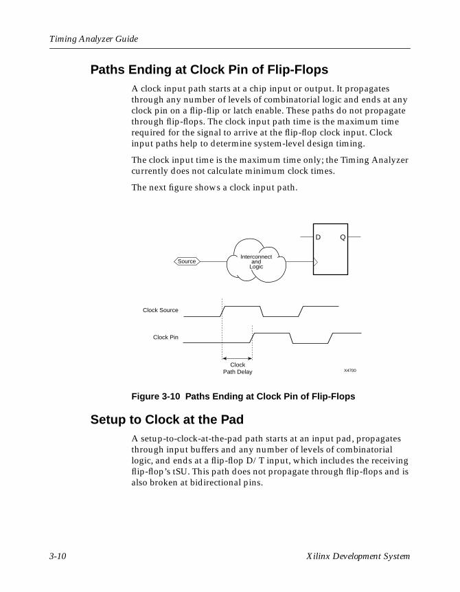
Paths Ending at Clock Pin of Flip-FlopsA clock input path starts at a chip input or output. It propagatesthrough any number of levels of combinatorial logic and ends at anyclock pin on a flip-flip or latch enable. These paths do not propagatethrough flip-flops. The clock input path time is the maximum timerequired for the signal to arrive at the flip-flop clock input. Clockinput paths help to determine system-level design timing.
The clock input time is the maximum time only; the Timing Analyzercurrently does not calculate minimum clock times.
The next figure shows a clock input path.
Figure 3-10 Paths Ending at Clock Pin of Flip-Flops
Setup to Clock at the PadA setup-to-clock-at-the-pad path starts at an input pad, propagatesthrough input buffers and any number of levels of combinatoriallogic, and ends at a flip-flop D/T input, which includes the receivingflip-flop’s tSU. This path does not propagate through flip-flops and isalso broken at bidirectional pins.
X4700
Clock Source
Clock Pin
ClockPath Delay
Interconnectand
LogicSource
D Q
3-10 Xilinx Development System

Timing Analysis
This delay reports tSU for data inputs relative to global or productterm clock inputs. It is calculated according to the following formulafor global and product term clocks.
tSU = Pad to Setup - Path Ending at Clock Pin ofFlip-Flop
Global clock paths start at global clock pads, propagate throughglobal clock buffers and end at a flip-flop clock pin. Product termclock paths start at input pads, propagate through a single level oflogic implemented in a clock product term, and end at the flip-flopclock pin. All three clock-at-the-pad paths are shown in the nextfigure.
Figure 3-11 Setup-to-Clock-at-the-Pad Path
Clock Pad to Output PadA clock-pad-to-output-pad path starts at input pads and tracethrough all paths that include a flip-flop clock input (except whenthat path includes a flip-flop asynchronous Set/Reset input) beforeending at an output pad. Clock-pad-to-output-pad paths tracethrough tristate controlled pad enable inputs.
Pad to PadA pad-to-pad path starts at an input pad of the chip, propagatesthrough one or more levels of combinatorial logic, and ends at anoutput pad of the chip. Combinatorial paths also trace through theenable inputs of tristate controlled pads. The pad-to-pad path time isthe maximum time required for the data to enter the chip, travelthrough logic and routing, and leave the chip. It is not controlled oraffected by any clock signal. A pad-to-pad path, along with a timingdiagram describing the path is displayed in the following figure.
X8011
QD
Pad-to-Setup Delay
Global or Product Term Clock Delay
REGOUT
clockBA
Timing Analyzer Guide 3-11

Timing Analyzer Guide
Figure 3-12 Pad-to-Pad Delay
Combinatorial paths are not traced through flip-flops. These pathsare also broken at bidirectional pins. A second representation isshown in the next figure.
Figure 3-13 Pad-to-Pad Path
Pad to SetupA pad-to-setup path starts at an input pad of the chip and ends at aD/T input to a flip-flop, latch, RAM, or the receiving flip-flop’s tSU,wherever there is a setup time against a control signal. Along theway, it propagates through input buffers and any number of combi-natorial logic levels. Pad-to-setup paths do not propagate throughflip-flops and are broken at bidirectional pins. The pad-to-setup pathtime is the maximum time required for the data to enter the chip,
interconnect and logic
X6191
logic and routing output
path delay
padpad
delayinput
delay
X8017
IN2OUT1
IN1
IN3
clock
QD
IN2
OUT2
IN1
3-12 Xilinx Development System

Timing Analysis
travel through logic and routing, and arrive at the output before theclock or control signal arrives. A pad-to-setup path and timingdiagram is shown in the following figure.
Figure 3-14 Pad-to-Setup Path
Design Analysis IssuesThe Timing Analyzer can help you resolve some of the mostfrequently encountered design problems. This section describescommon problems and solutions.
Feedback LoopsAsynchronous feedback paths in a design can cause many paths to bereported that may not actually be timing problems. The mostcommon cases are feedback paths through asynchronous Set or Resetto banks of flip-flops, like a state machine or a counter. Anotherexample is the construction of latches from function generators,which are built using asynchronous feedback paths.
interconnect and logic
X6189
D Q
clock
clock
valid valid
input delay
logic and routing delay
flip-flop setup
path delay
minimum clock period
pad
external margin
Timing Analyzer Guide 3-13
Timing Analyzer Guide
To exclude specific nets that create feedback paths, such as an illegal-state Reset logic loop for a state machine, you can use the ExcludePaths with Nets command to exclude any paths that contain thosenets from the timing report.
With the Control Path Tracing command, you can control some asyn-chronous points through logic; for example, you can exclude theasynchronous Reset of a flip-flop or TBUF input to output.
Timing ConstraintsIf you entered timing constraints before compiling your design withthe mapper, you can use the Timing Analyzer to verify whether yourconstraints were met. The following example of portions of a TimingAnalysis report shows how the Timing Analyzer finds paths that didnot meet timing constraints; five errors occurred and threeconstraints were not met.
=========================================================================
Timing constraint: TS01 = MAXDELAY FROM TIMEGRP"FFS" TO
TIMEGRP "FFS"
2000.000000 pS PRIORITY 0 ;
1 item analyzed, 1 timing error detected.
Maximum delay is 3.340ns.
-------------------------------------------------------------------------
Slack: -1.340ns path $1N11 to $1N11 relative to
2.000ns delay constraint
Path $1N11 to $1N11 contains 2 levels of logic:
Path starting from Comp: CLB.K (from $1N19)
3-14 Xilinx Development System

Timing Analysis
To Delay type Delay(ns)Physical Resource
Logical Resource(s)
---------------------------------------------------------
CLB.XQ Tcko 1.830R$1N11
$1N11
CLB.F2 net (fanout=2) e 0.380R$1N11
CLB.K Tick 1.130R$1N11
$1N15
$1N11
-------------------------------------------------
Total (2.960ns logic, 0.380ns route) 3.340ns(to $1N19)
(88.6% logic, 11.4% route)
.
.
.
3 constraints not met.
Timing Analyzer Guide 3-15

Timing Analyzer Guide
Data Sheet report:
-----------------
All values displayed in nanoseconds (ns)
Setup/Hold to clock ck1_i
---------------+------------+------------+
| Setup to | Hold to |
Source Pad | clk (edge) | clk (edge) |
---------------+------------+------------+
res_i | 6.202(R)| |
start_i | 2.213(R)| 0.000(R)|
---------------+------------+------------+
.
.
.
Table of Timegroups:
-------------------
TimeGroup PADS:
BELs:
OUT D C CLR
3-16 Xilinx Development System

Timing Analysis
TimeGroup FFS:
BELs:
$1N11
Timing summary:
---------------
Timing errors: 5 Score: 15874
Constraints cover 5 paths, 0 nets, and 5connections (100.0% coverage)
Design statistics:
Maximum path delay from/to any node: 10.716ns
Analysis completed Wed Feb 24 14:29:35 1999
-------------------------------------------------------------------------
Clock SkewThe Timing Analyzer can report clock skew, which is the differencebetween the time a clock signal arrives at the source flip-flop in a pathand the time it arrives at the destination flip-flop on the same clocknet. Clock skew occurs most often when global routing is not used toroute clock nets, because other routing is less predictable. The arrivalof clock signals at different times can affect the required clock period.This section describes negative and positive clock skew and how theTiming Analyzer reports clock skew.
Timing Analyzer Guide 3-17

Timing Analyzer Guide
Negative Clock Skew
When the destination is clocked before the source, the clock skew iscalled negative clock skew. Negative clock skew means that the clockperiod must be longer than the path delay plus the amount of clockskew between the flip-flops. Negative clock skew is illustrated in thenext figure.
Figure 3-15 Negative Clock Skew
Positive Clock Skew
When the source is clocked first, the clock skew is called positiveclock skew. Positive clock skew means that the clock period could beshorter than the path delay by the minimum amount of clock skew.The Timing Analyzer does not account for positive clock skew; ittruncates positive clock skew to zero. Positive clock skew is illus-trated in the following figure.
interconnect and logic
X6194
D QD
clock
clock at FF1
clock at FF2
valid valid
Q
clock to
output
logic and routing
delay
Flip-flop setup
path delay
minimum clock period
FF1 FF2
clock skew
3-18 Xilinx Development System

Timing Analysis
Figure 3-16 Positive Clock Skew
During Timing Analysis
The Timing Analyzer uses the timing constraints specified in thePhysical Constraints File (FPGAs) or the VM6 design file (CPLD); itdoes not infer extra timing constraints. The Timing Analyzeraccounts for clock skew for all register to register paths. Thefollowing example shows the clock skew portion of a AnalyzeAgainst Timing Constraints Analysis report.
Slack: 12.667ns path SOURCE to DEST relative to
4.633ns total path delay
-2.300ns clock skew
interconnectandlogic
X6195
D QD
clock
clock at FF1
clock at FF2
valid valid
Q
clockto
output
logic and routingdelay
flip-flopsetup
path delay
minimum clock period
FF1 FF2
clock skew
Timing Analyzer Guide 3-19

Timing Analyzer Guide
15.000ns delay constraint
Path SOURCE to DEST contains 2 levels of logic:
Path starting from Comp: CLB_R14C13.K (fromSIG_CLK)
To Delay type Delay(ns)Physical Resource
Logical Resource(s)
------------------------------------------------- --------
CLB_R14C13.YQ Tcko 2.090R SOURCE
BEL_SOURCE.FFY
CLB_R14C14.C4 net (fanout=1) 1.533RDATA_SRC_DST
CLB_R14C14.K Tdick 1.010R DEST
BEL_DEST.FFY
-------------------------------------------------
Total (3.100ns logic, 1.533ns route) 4.633ns(to SIG_CLK)
(66.9% logic, 33.1% route)
You can use Analyze → Query Nets to generate a Query Netsreport to display the clock skew across specific clock nets. See the“Querying for Information” section of the “Using the TimingAnalyzer” chapter for the procedure to generate a Query NetsReport, an example of a Query Nets Report, and information on thereport format.
3-20 Xilinx Development System

Timing Analysis
Off-Chip DelayTo determine system-level clock speed, you must add any externaldelay to paths that travel off-chip. This way, the Timing Analyzerincludes this external delay when calculating the delay for the path.There is no default delay; the Timing Analyzer does not add off-chipdelay unless you specify it. See the XILINX Software Conversion Guidefrom XACTstep v5.x.x to XACTstep vM!.x.x for information on how tospecify these delays with the OFFSET constraint in the UCF (UserConstraints File) file.
Timing Analyzer Guide 3-21

Timing Analyzer Guide
3-22 Xilinx Development System

Chapter 4
Using the Timing Analyzer
This chapter describes the various functions you can perform withthe Timing Analyzer. It contains the following main sections.
• “Opening a Design”
• “Apply Physical Constraints Files”
• “Viewing Settings”
• “Viewing Clocks”
• “Querying for Information”
• “Creating Reports”
• “Specifying Report Appearance and Content”
• “Changing the Speed Grade”
• “Using Path Filtering Commands”
• “Using the Console Window”
• “Using Macros”
Note The commands and dialog boxes in this chapter are used in thecontext of procedures, but they are not explained in detail. For adetailed explanation of them, see the Timing Analyzer Online HelpMenu Commands.
Opening a DesignBefore you can create a timing report using the Timing Analyzer, loada mapped NCD (FPGA) or a completed placed and routed VM6(CPLD) design file. The NCD (FPGA) can be mapped, placed, orrouted. To open a design for timing analysis, follow these steps.
Timing Analyzer Guide — 3.1i 4-1

Timing Analyzer Guide
1. Select File → Open Design , or click on the Open Designtoolbar button.
The Open Design dialog box appears, as shown in the followingfigure.
2. You can also enter a file name in the Physical Constraints FileField or use the Browse button to select a PCF file. If you do notenter a constraints file, Timing Analyzer looks for a physicalconstraints file with the same name as the design file, but with a.pcf extension
3. The Open dialog box appears.
4. The In the Look in/Directories list box, click on the directorycontaining the NCD (FPGA) or VM6 (CPLD) file to load.
5. Under Files of Type/List Files of Type, click on the pull-down thelist box and select FPGA Designs (*.ncd) or CPLD Designs(*.vm6).
All the available NCD or VM6 files are displayed in the list box.
6. Select an NCD or a VM6 file from the list box, or type the name inthe field below File Name. (*.ncd appears by default; backspaceover the asterisk before typing in the design file name.)
4-2 Xilinx Development System

Using the Timing Analyzer
7. Click OK.
The Timing Analyzer reads your design and device information,processes any timing constraints, and then loads your design. ForFPGA designs, the Timing Analyzer also reads the .pcf physicalconstraints file with the same name as the design file, if one existsin the same directory as the design file (the PCF file containsphysical constraints information). The order of the constraints inthe PCF file is reflected by the Timing Analyzer.
When your design is loaded, the path name and design file nameappear at the top of the Timing Analyzer window.
You can now create a timing report. Refer to the “Creating Reports”section for instructions on this procedure.
WarningIf you open a design when another design is open, the TimingAnalyzer resets the current settings to the defaults. If you re-opena design that is already open, the Timing Analyzer also resets thecurrent settings to the defaults and opens the default PCF, if itexists.
Apply Physical Constraints FilesPhysical Constraints Files (PCF) contain physical constraint informa-tion. They apply only to FPGAs, because CPLD timing information iscontained in the (VM6) design file itself. The order of the timingconstraints in the PCF file is reflected by the Timing Analyzer. Thissection describes methods for loading and opening PhysicalConstraints Files.
Manually Opening a Physical Constraints FileIf you already have a design open and wish to load a different Phys-ical Constraints File for use with the current design, follow thesesteps.
1. Select File → Apply Physical Constraints .
The Open Physical Constraints dialog box appears.
2. In the Look in/Directories list box, click on the directorycontaining the PCF file to load.
Timing Analyzer Guide 4-3

Timing Analyzer Guide
3. Under Files of Type/List Files of Type, Physical Constraints(*.pcf) is the default and the only file type you can select.
All the available PCF files are displayed in the list box.
4. Select a PCF file from the list box, or type the name in the fieldbelow File name. (*.pcf appears by default; backspace over theasterisk before typing in the physical constraints file name.)
5. Click OK.
The Timing Analyzer reads the PCF file and the path nameappears on the right side of the status bar at the bottom of theTiming Analyzer window.
Viewing a Physical Constraints FileIn some cases you may want to open a PCF file for viewing fromwithin the Timing Analyzer. When you open a PCF file by thismethod, the Timing Analyzer does not load the PCF file for use withthe current design. It just opens the file for viewing but does notreplace the PCF file that is loaded for use with the current design. Toopen a PCF file in this way, follow these steps.
1. Select File → Open →Physical Constraints File .
The Open Physical Constraints dialog box appears.
2. Under Files of Type/List Files of Type, select All Files (*.*).
3. Select a PCF file from the list box, or type it in the field below FileName.
4. Click OK.
The PCF file is displayed in a window but the path name on theright side of the status bar at the bottom of the Timing Analyzerwindow does not change since opening a PCF file by this methoddoes not load the PCF file for processing with the current design.
Viewing SettingsTo view current Timing Analyzer settings, select View →Settings .
4-4 Xilinx Development System

Using the Timing Analyzer
The Timing Analyzer displays a pop-up window with the currentsettings and options. The following figure displays an example of theSettings window.
Figure 4-1 Settings Window
When this window is the active window and you change an optionsetting or a path filter, the change is immediately reflected in thewindow. If it is not the active window and you change an option or afilter, you must click inside the Settings window to update it auto-matically.
The contents of the window can be saved as an .xtm file to save thesettings as a macro to return the system to the same state as when thesettings were saved. See the “Saving a New Macro” and the“Running a Macro” sections for more information. You can also savethe contents of the window to a .twr file. TWR files are listed asTiming Analysis Reports (*.twr) under List Files of Type in File menucommand dialog boxes. See the “Saving a Report” section for theprocedure to save a report.
Timing Analyzer Guide 4-5

Timing Analyzer Guide
Viewing ClocksThe Clocks report lists the names of all of the clocks in the design. Togenerate a Clocks report, select View → Clocks . The TimingAnalyzer displays the Clocks report in a pop-up window. You cansave the contents of the window as a (.twr) file. TWR files are listed asTiming Analysis Reports (*.twr) under List Files of Type in File menucommand dialog boxes. See the “Saving a Report” section for theprocedure to save a report.
Querying for InformationYou may want to focus on the source, destination, and timing of aparticular net or time group. You can obtain information about thetiming of particular nets or the members of a time group using theQuery commands. These commands only applies to FPGAs; it isdisabled if a CPLD design is open.
To perform a query, follow this procedure.
1. Select Analyze → Query Nets or Analyze → QueryTimegroups .
The Query Nets or Query Timegroups dialog box appearsdepending on your selection.
2. The following information is generated for each option.
♦ Nets — The Timing Analyzer shows the fanout, the timingfrom the source CLB to each of the destination CLBs, and theCLB names in the generated Query Nets Report.
♦ TimeGroups — The Timing Analyzer lists the elements in thespecified timing groups in the generated Query TimeGroupsReport.
3. If you select Nets, enter a value in the Delay Greater Than field ofthe Filter for Available Nets.
The Delay Greater Than value specifies a minimum net delay innanoseconds. The Timing Analyzer displays only those pathsthat have a delay greater than or equal to the specified value.
4. Enter a filter in the other portion of the Filter for Available Nets/TimeGroups section, if desired, and click Apply .
4-6 Xilinx Development System

Using the Timing Analyzer
If you enter a value in the Delay Greater Than and a filter in thefilter field, the Timing Analyzer lists the nets that meet bothcriteria.
5. Select the nets or timing groups that you want to query from theAvailable Nets/TimeGroups list box and move specific ones orall of them to the Selected Nets/TimeGroups list box.
See the “Common Fields” section of the “Getting Started”chapter for details on selecting and moving items between listboxes.
6. Click OK.
The Timing Analyzer displays the Query Nets/TimeGroupsReport in a pop-up window, which can be saved as a TWR file.Nets/TimeGroups is Nets or TimeGroups, corresponding withyour dialog box selection in step 1. See the “Saving a Report”section for the procedure to save a report.
Query Nets ReportThe following is an example of Query Nets Report.
M-- $1N15 ................ $1I37.O................ 4.0 $1N6.F4 $1I45.O 4.0 $1N6.F4--- $1N32 ................ C.I2................... 2.0 $1I45.T 2.0 $1N6.F3--- $1N34 ................ D.I2................... 1.0 $1N6.F1--- $1N6 ................. $1N6.X................. 1.0 O1.O 1.0 O2.O--- $1N51 ................ A1.I2.................. 0.0 $1I45.I--- $1N38 ................ B.I2................... 2.0 $1I37.T--- $1N41 ................ A.I2................... 2.0 $1I37.I
The contents of the Query Nets Report example have been placed inthe following table to illustrate the format of the report. Connectionsare listed by net, then by source; each is only listed once. Explana-
Timing Analyzer Guide 4-7

Timing Analyzer Guide
tions of the information in Net Characteristics and Delay columnsfollow the table.
Net Characteristics
The entries in the Net Characteristics column are comprised of threecharacters. The characters indicate aspects of the net(s) you query.Each character position is independent of the others. The characterposition and values of each position are illustrated in this table.
Delay Value
The entries in the Delay Value column can include asterisks (*), ques-tion marks (?), or tildes (~).
• The pin is unrouted or one or both pins are not yet placed if threeasterisks (***) appear as the delay value. An asterisk preceding a
Table 4-1 Query Nets Report Format
NetCharacteristics
Net NameDriver PinName
Delay Value Load Pin Name
M-- $1N15 $1I37.O 4.0 $1N6.F4
$1I45.O 4.0 $1N6.F4
--- $1N32 C.I2 2.0 $1I45.T
2.0 $1N6.F3
--- $1N34 D.I2 1.0 $1N6.F1
--- $1N6 $1N6.X 1.0 O1.O
1.0 O2.O
--- $1N51 A1.I2 0.0 $1I45.I
--- $1N38 B.I2 2.0 $1I37.T
--- $1N41 A-I2 2.0 $1I37.I
Left = Net Source Middle = Net Load Right = If Critical
S = No Source L = No Load C = Net marked withCRITICAL propertyin the design or NetPRI is ≥ 10
M = Multiple Sources - = Not Critical
4-8 Xilinx Development System

Using the Timing Analyzer
number, *3 for example, indicates the connection delay is esti-mated, if timing analysis is performed on an unrouted design.Because the Timing Analyzer can perform timing analysis onmapped FPGA designs, generating a Query Nets report candetermine if a design does not meet timing requirements before adesign is routed.
• A question mark (?) indicates the net was routed incorrectly.
• A tilde (~) preceding a delay value indicates that the delay valueis approximate. The delay can be longer than estimated.
Query Time Groups Report
The Query Time Groups report lists the contents of each time groupthat you select. Time group information is also generated in theTiming Constraints Analysis report.
Creating ReportsAfter you load a design file, you can decide what kind of report youwant to generate. This section describes how to create all the reportsavailable in the Timing Analyzer as well as how to save and printthem.
With the Find command on the Edit menu, you can search for specifictext strings in reports. Directions for this procedure are given in the“Searching for Text in a Report” section.
The Timing Analyzer has default settings that you can change usingfilters with various commands. Filters modify the scope of generatedreports by specifying which paths you want to analyze. For moreinformation, refer to the “Using Path Filtering Commands” section.To view the current settings, refer to the “Viewing Settings” section.
Timing Constraints AnalysisThe Timing Constraints Analysis report compares the design’sperformance to the timing constraints.
There are several ways to generate a Timing Constraints Analysisreport. You can use the following toolbar button to generate a TimingConstraints Analysis report.
Timing Analyzer Guide 4-9

Timing Analyzer Guide
In addition to the button the Analyze → Against TimingConstraints dialog box includes the Timing Constraints tab thatcontains the following radio button options.
• Report paths against timing constraints
• Report failing paths against timing constraints
To generate a Timing Constraints Analysis report, select one of theprevious options.
This command has an interrupt function when analyzing FPGAdesigns. A Timing Analysis in Progress dialog box with an Abortbutton appears.
Clicking the Abort button, the Esc key, or the Enter/Return keyaborts the analysis and no report is generated or displayed.
In addition to using the above commands, you can use the followingpath filter options commands to modify the Timing Constraints Anal-ysis report (See “Using Path Filtering Commands” section of the“Using the Timing Analyzer” chapter for more details).
• Disable Timing Constraints (Timing Constraints tab)
• Include Paths with Nets (Filter Paths by Net tab)
• Exclude Paths with Nets (Filter Paths by Net tab)
After processing the design, the Timing Analyzer displays the TimingConstraints Analysis report in a pop-up window. The contents of thewindow can be saved as a TWR file; see the “Saving a Report” sectionfor the procedure to save a report. Following is an example of aTiming Constraints Analysis report.
-------------------------------------------------------------------------
4-10 Xilinx Development System

Using the Timing Analyzer
Timing Analyzer 2.1iCopyright (c) 1995-1999 Xilinx, Inc. All rights reserved.
Design file: testclk.ncdPhysical constraint file: testclk.pcfDevice,speed: xcv100,-5 (x1_0.71 1.76 Advanced)Report level: verbose report, limited to 1 item perconstraint-------------------------------------------------------------------------
=========================================================================Timing constraint: TS_ck1_i = PERIOD TIMEGRP "ck1_i" 20 nSHIGH 50.000 % ; 955 items analyzed, 0 timing errors detected. Minimum period is 14.655ns.-------------------------------------------------------------------------Slack: 5.345ns path core_inst1/counter1/cont<1> to core_inst1/counter1/cont<9> relative to 20.000ns delay constraintPath core_inst1/counter1/cont<1> to core_inst1/counter1/cont<9>contains 12 levels of logic:Path starting from Comp: CLB_R10C8.S0.CLK (from ck1)To Delay type Delay(ns) Physical Resource
Logical Resource(s)
------------------------------------------------- --------CLB_R10C8.S0.YQ Tcko 1.203R core_inst1/counter1/
cont<1>core_inst1/
counter1/cont_reg<1>
CLB_R11C10.S0.G1 net (fanout=5) 3.073R core_inst1/counter1/
cont<1>CLB_R11C10.S0.COUT Topcyg 1.545R core_inst1/counter1/C9/
C3/C1/O C369
Timing Analyzer Guide 4-11

Timing Analyzer Guide
core_inst1/counter1/
C9/C3/C1...CLB_R9C10.S1.F1 net (fanout=1) 1.491R core_inst1/counter1/N362CLB_R9C10.S1.CLK Tas 1.043R core_inst1/counter1/
cont<9>C303core_inst1/
counter1/cont_reg<9>
-------------------------------------------------Total (6.638ns logic, 8.017ns route) 14.655ns (to ck1)
(45.3% logic, 54.7% route)-------------------------------------------------------------------------...All constraints were met.
Data Sheet report:-----------------All values displayed in nanoseconds (ns)
Setup/Hold to clock ck1_i---------------+------------+------------+ | Setup to | Hold to |Source Pad | clk (edge) | clk (edge) |---------------+------------+------------+res_i | 6.202(R)| |start_i | 2.213(R)| 0.000(R)|---------------+------------+------------+
Setup/Hold to clock ck2_i---------------+------------+------------+ | Setup to | Hold to |
4-12 Xilinx Development System
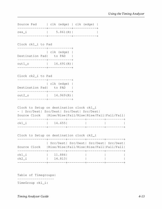
Using the Timing Analyzer
Source Pad | clk (edge) | clk (edge) |---------------+------------+------------+res_i | 5.861(R)| |---------------+------------+------------+
Clock ck1_i to Pad---------------+------------+ | clk (edge) |Destination Pad| to PAD |---------------+------------+out1_o | 16.691(R)|---------------+------------+
Clock ck2_i to Pad---------------+------------+ | clk (edge) |Destination Pad| to PAD |---------------+------------+out2_o | 14.969(R)|---------------+------------+
Clock to Setup on destination clock ck1_i- | Src/Dest| Src/Dest| Src/Dest| Src/Dest|Source Clock |Rise/Rise|Fall/Rise|Rise/Fall|Fall/Fall|---------------+---------+---------+---------+---------+ck1_i | 14.655| | | |---------------+---------+---------+---------+---------+
Clock to Setup on destination clock ck2_i---------------+---------+---------+---------+---------+ | Src/Dest| Src/Dest| Src/Dest| Src/Dest|Source Clock |Rise/Rise|Fall/Rise|Rise/Fall|Fall/Fall|---------------+---------+---------+---------+---------+ck1_i | 11.886| | | |ck2_i | 14.813| | | |---------------+---------+---------+---------+---------+
Table of Timegroups:-------------------TimeGroup ck1_i:
Timing Analyzer Guide 4-13

Timing Analyzer Guide
BELs: core_inst1/counter1/regist1_reg<0> core_inst1/counter1/regist1_reg<1> core_inst1/counter1/regist1_reg<2> core_inst1/counter1/regist1_reg<3> core_inst1/counter1/regist1_reg<4> core_inst1/counter1/regist1_reg<5> core_inst1/counter1/regist1_reg<6> core_inst1/counter1/regist1_reg<7> core_inst1/counter1/regist1_reg<8> core_inst1/counter1/regist1_reg<9> core_inst1/counter1/regist0_reg<0> core_inst1/counter1/regist0_reg<1>core_inst1/counter1/regist0_reg<2> core_inst1/counter1/regist0_reg<3> core_inst1/counter1/regist0_reg<4> core_inst1/counter1/regist0_reg<5> core_inst1/counter1/regist0_reg<6> core_inst1/counter1/regist0_reg<7> core_inst1/counter1/regist0_reg<8> core_inst1/counter1/regist0_reg<9> core_inst1/counter1/cont_reg<0> core_inst1/counter1/cont_reg<1> core_inst1/counter1/cont_reg<2> core_inst1/counter1/cont_reg<3> core_inst1/counter1/cont_reg<4> core_inst1/counter1/cont_reg<5> core_inst1/counter1/cont_reg<6> core_inst1/counter1/cont_reg<7> core_inst1/counter1/cont_reg<8> core_inst1/counter1/cont_reg<9>
TimeGroup ck2_i:BELs: core_inst2/counter1/regist1_reg<0> core_inst2/counter1/regist1_reg<1> core_inst2/counter1/regist1_reg<2> core_inst2/counter1/regist1_reg<3> core_inst2/counter1/regist1_reg<4> core_inst2/counter1/regist1_reg<5> core_inst2/counter1/regist1_reg<6> core_inst2/counter1/regist1_reg<7> core_inst2/counter1/regist1_reg<8> core_inst2/counter1/regist1_reg<9> core_inst2/counter1/regist0_reg<0> core_inst2/counter1/regist0_reg<1> core_inst2/counter1/regist0_reg<2> core_inst2/counter1/regist0_reg<3> core_inst2/counter1/regist0_reg<4> core_inst2/counter1/regist0_reg<5> core_inst2/counter1/regist0_reg<6> core_inst2/counter1/regist0_reg<7> core_inst2/counter1/regist0_reg<8> core_inst2/counter1/regist0_reg<9> core_inst2/counter1/cont_reg<0> core_inst2/counter1/cont_reg<1> core_inst2/counter1/cont_reg<2> core_inst2/counter1/cont_reg<3> core_inst2/counter1/cont_reg<4> core_inst2/counter1/cont_reg<5> core_inst2/counter1/cont_reg<6>
4-14 Xilinx Development System

Using the Timing Analyzer
core_inst2/counter1/cont_reg<7> core_inst2/counter1/cont_reg<8> core_inst2/counter1/cont_reg<9>
Timing summary:---------------
Timing errors: 0 Score: 0
Constraints cover 2184 paths, 0 nets, and 380 connections (100.0%coverage)
Design statistics: Minimum period: 14.813ns (Maximum frequency: 67.508MHz)
Minimum input arrival time before clock: 6.202ns Minimum output required time after clock: 16.691ns
Analysis completed Fri Mar 12 12:10:11 1999------------------------------------------------------------------------
Analyze Against Auto Generated Design ConstraintsAnalysis Report
The Analyze Against Auto Generated Design Constraints Analysisreport provides a set of summary statistics for the paths from thetiming requirements submitted for analysis. This report is essentiallyan error report that displays a summary header for each constraintwhether it passes or not and lists paths in error for constraints thatare violated.
If the PCF file contains no constraints, the Analyze Against AutoGenerated Design Constraints Analysis report creates four basicconstraints: PERIOD, OFFSET IN, OFFSET OUT, and PAD TO PAD.
To generate an Analyze Against Auto Generated Design ConstraintsAnalysis report, select Analyze → Analyze Against AutoGenerated Design Constraints , or click on the AnalyzeAgainst Auto Generated Design Constraints button in the toolbar.
Timing Analyzer Guide 4-15

Timing Analyzer Guide
This command has an interrupt function when analyzing FPGAdesigns. A Timing Analysis in Progress dialog box with an Abortbutton appears.
Clicking the Abort button, the Esc key, or the Enter/Return keyaborts the analysis. A report is not generated or displayed.
After processing the design, the Timing Analyzer displays theAnalyze Against Auto Generated Design Constraints Analysis reportin a pop-up window. The contents of the window can be saved as aTWR file; see the “Saving a Report” section for the procedure to savea report. Following is an example of an FPGA Analyze Against AutoGenerated Design Constraints Analysis report.
-------------------------------------------------------------------------Timing Analyzer 2.1iCopyright (c) 1995-1999 Xilinx, Inc. All rights reserved.
Design file: C:\designs\loop.ncdPhysical constraint file: C:\designs\loop.pcfDevice,speed: xc4036ex,-3 (x1_0.08 3.7f )Report level: error report, limited to 1 item perconstraint-------------------------------------------------------------------------
=========================================================================Timing constraint: TS01 = MAXDELAY FROM TIMEGRP "FFS" TOTIMEGRP "FFS"
4-16 Xilinx Development System

Using the Timing Analyzer
2000.000000 pS PRIORITY 0 ; 1 item analyzed, 0 timing errors detected. Maximum delay is 3.340ns.-------------------------------------------------------------------------
=========================================================================Timing constraint: TS02 = MAXDELAY FROM TIMEGRP "PADS" TOTIMEGRP "FFS"1500.000000 pS PRIORITY 0 ; 3 items analyzed, 3 timing errors detected. Maximum delay is 4.006ns.-------------------------------------------------------------------------Slack: -2.506ns path D to $1N11 relative to 1.500ns delay constraint
Path D to $1N11 contains 2 levels of logic:Path starting from Comp: IOB.PADTo Delay type Delay(ns) Physical Resource
Logical Resource(s)
------------------------------------------------- --------IOB.I1 Tpid 1.810R D D $1N13CLB.F1 net (fanout=1) e 1.066R $1N13CLB.K Tick 1.130R $1N11 $1N15 $1N11-------------------------------------------------Total (2.940ns logic, 1.066ns route) 4.006ns (to $1N19) (73.4% logic, 26.6% route)
-------------------------------------------------------------------------
=================================================================
Timing Analyzer Guide 4-17

Timing Analyzer Guide
========Timing constraint: TS03 = MAXDELAY FROM TIMEGRP "FFS" TOTIMEGRP "PADS"2500.000000 pS PRIORITY 0 ; 1 item analyzed, 1 timing error detected. Maximum delay is 10.716ns.-------------------------------------------------------------------------Slack: -8.216ns path $1N11 to OUT relative to 2.500ns delay constraint
Path $1N11 to OUT contains 2 levels of logic:Path starting from Comp: CLB.K (from $1N19)To Delay type Delay(ns) Physical Resource
Logical Resource(s)
------------------------------------------------- --------CLB.XQ Tcko 1.830R $1N11 $1N11IOB.O net (fanout=2) e 1.066R $1N11IOB.PAD Tops 7.820R OUT OUT.OUTBUF OUT-------------------------------------------------Total (9.650ns logic, 1.066ns route) 10.716ns (90.1% logic, 9.9% route)
-------------------------------------------------------------------------
2 constraints not met.
Data Sheet report:-----------------All values displayed in nanoseconds (ns)
Setup/Hold to clock ck1_i---------------+------------+------------+
4-18 Xilinx Development System

Using the Timing Analyzer
| Setup to | Hold to |Source Pad | clk (edge) | clk (edge) |---------------+------------+------------+res_i | 6.202(R)| |start_i | 2.213(R)| 0.000(R)|---------------+------------+------------+...
Table of Timegroups:-------------------TimeGroup PADS:BELs: OUT D C CLR
TimeGroup FFS:BELs: $1N11
Timing summary:---------------
Timing errors: 4 Score: 15874
Constraints cover 5 paths, 0 nets, and 5 connections (100.0%coverage)
Design statistics: Maximum path delay from/to any node: 10.716ns
Analysis completed Wed Mar 3 14:30:42 1999-------------------------------------------------------------------------
Timing Analyzer Guide 4-19
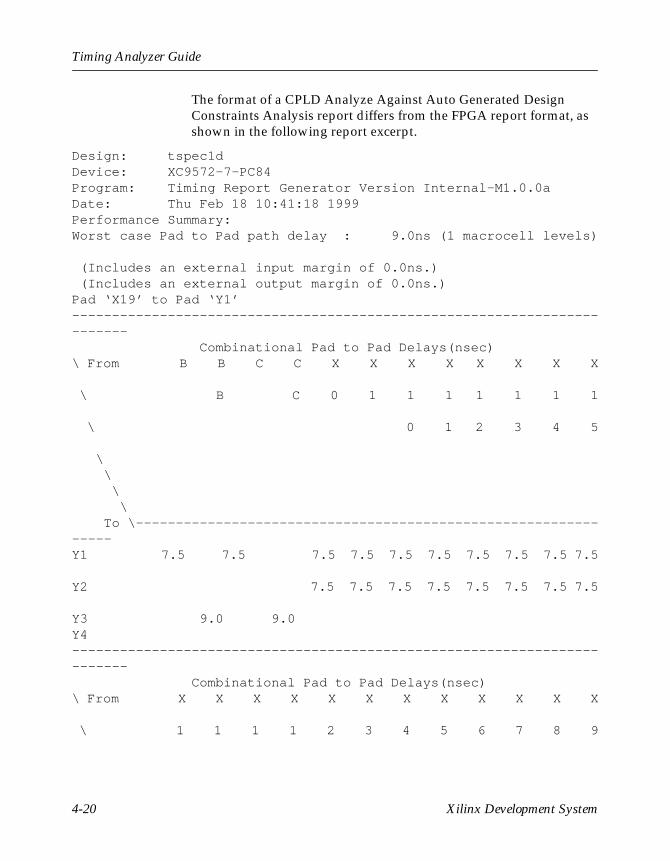
Timing Analyzer Guide
The format of a CPLD Analyze Against Auto Generated DesignConstraints Analysis report differs from the FPGA report format, asshown in the following report excerpt.
Design: tspec1dDevice: XC9572-7-PC84Program: Timing Report Generator Version Internal-M1.0.0aDate: Thu Feb 18 10:41:18 1999Performance Summary:Worst case Pad to Pad path delay : 9.0ns (1 macrocell levels)
(Includes an external input margin of 0.0ns.) (Includes an external output margin of 0.0ns.)Pad ‘X19’ to Pad ‘Y1’------------------------------------------------------------------------- Combinational Pad to Pad Delays(nsec)\ From B B C C X X X X X X X X
\ B C 0 1 1 1 1 1 1 1
\ 0 1 2 3 4 5
\ \ \ \ To \---------------------------------------------------------------Y1 7.5 7.5 7.5 7.5 7.5 7.5 7.5 7.5 7.5 7.5
Y2 7.5 7.5 7.5 7.5 7.5 7.5 7.5 7.5
Y3 9.0 9.0Y4------------------------------------------------------------------------- Combinational Pad to Pad Delays(nsec)\ From X X X X X X X X X X X X
\ 1 1 1 1 2 3 4 5 6 7 8 9
4-20 Xilinx Development System

Using the Timing Analyzer
\ 6 7 8 9 \ \ \ \ To \----------------------------------------------------------------Y1 7.5 7.5 9.0 9.0 7.5 7.5 7.5 7.5 7.5 7.5 7.5 7.5
Y2 7.5 7.5 7.5 7.5 7.5 7.5 7.5 7.5
Y3Y4...Path Type Definition:Pad to Pad (tPD) - Reports pad to pad pathsthat start
at input pads and end at output pads.Paths are not traced through
registers.Clock Pad to Output Pad (tCO) - Reports paths that start atinput
pads trace through clock inputs ofregisters and end at output pads.
Paths are not traced through PRE/CLR inputs of registers.
Setup to Clock at Pad (tSU) - Reports external setup timeof data
to clock at pad. Data path starts atan input pad and end at register D/T
input. Clock path starts at input padand ends at the register clock input.
Paths are not traced through registers.
Clock to Setup (tCYC) - Register to register cycle time.Include source register tCO and
destination register tSU.
Timing Analyzer Guide 4-21

Timing Analyzer Guide
You can use the following path filtering commands to modify thescope of the Analyze Against Auto Generated Design ConstraintsAnalysis report.
• Include Paths with Nets (Filter Paths by Net tab)
• Exclude Paths with Nets (Filter Paths by Net tab)
• Path Tracing (Path Tracing tab)
Analyze Against User Specified Paths by DefiningEndpoints Analysis Report
The Analyze Against User Specified Paths by Defining Endpointsreport displays a detailed analysis of all specified paths. It containsthe worst-case path delays for all paths that are not filtered out.
To generate a Analyze Against User Specified Paths by DefiningEndpoints report, select Analyze → Analyze Against UserSpecified Paths by Defining Endpoints , or click on theAnalyze Against User Specified Paths by Defining Endpoints buttonin the toolbar.
This command has an interrupt function when analyzing FPGAdesigns. A Timing Analysis in Progress dialog box with an Abortbutton appears.
Clicking the Abort button, the Esc key, or the Enter/Return keyaborts the analysis. A report is neither generated nor displayed.
After processing the design, the Timing Analyzer displays theAnalyze Against User Specified Paths by Defining Endpoints reportin a pop-up window. The contents of the window can be saved as aTWR file; see the “Saving a Report” section for the procedure to savea report. Following is an example of this report.
4-22 Xilinx Development System

Using the Timing Analyzer
-------------------------------------------------------------------------Timing Analyzer 2.1iCopyright (c) 1995-1999 Xilinx, Inc. All rights reserved.
Design file: C:\designs\loop.ncdDevice,speed: xc4036ex,-3 (x1_0.08 3.7f )Report level: verbose report, limited to 1 item perconstraint-------------------------------------------------------------------------
=========================================================================Timing constraint: PATH "PATHFILTERS" = FROM TIMEGRP"SOURCES" TO TIMEGRP"DESTINATIONS" ; 5 items analyzed, 0 timing errors detected. Maximum delay is 10.716ns.-------------------------------------------------------------------------Delay: 10.716ns $1N11 to OUT
Path $1N11 to OUT contains 2 levels of logic:Path starting from Comp: CLB.K (from $1N19)To Delay type Delay(ns) Physical Resource
Logical Resource(s)
------------------------------------------------- --------CLB.XQ Tcko 1.830R $1N11 $1N11IOB.O net (fanout=2) e 1.066R $1N11IOB.PAD Tops 7.820R OUT OUT.OUTBUF OUT-------------------------------------------------Total (9.650ns logic, 1.066ns route) 10.716ns (90.1% logic, 9.9% route)
Timing Analyzer Guide 4-23

Timing Analyzer Guide
-------------------------------------------------------------------------
All constraints were met.
Data Sheet report:-----------------All values displayed in nanoseconds (ns)
Setup/Hold to clock ck1_i---------------+------------+------------+ | Setup to | Hold to |Source Pad | clk (edge) | clk (edge) |---------------+------------+------------+res_i | 6.202(R)| |start_i | 2.213(R)| 0.000(R)|---------------+------------+------------+...
Table of Timegroups:-------------------TimeGroup SOURCES:BELs: $1N11 OUT D C CLR
TimeGroup DESTINATIONS:BELs: $1N11 OUT D C CLR
Timing summary:---------------
Timing errors: 0 Score: 0
4-24 Xilinx Development System
Using the Timing Analyzer
Constraints cover 5 paths, 0 nets, and 5 connections (100.0%coverage)
Design statistics: Maximum path delay from/to any node: 10.716ns
Analysis completed Wed Mar 3 14:31:19 1999-------------------------------------------------------------------------
You can use the following path filtering commands from the analyzetabs to modify the scope of the Analyze Against User Specified Pathsby Defining Endpoints report.
• Select Sources (Path Endpoints tab)
• Select Destinations (Path Endpoints tab)
• Include Paths with Nets (Filter Paths by Net tab)
• Exclude Paths with Nets (Filter Paths by Net tab)
• Path Tracing (Path Tracing tab)
Viewing a ReportWhen a Timing Analysis report (TWR file) is opened in the TimingAnalyzer window, the report window contains three sub-windows,as shown in the following figure.
Timing Analyzer Guide 4-25

Timing Analyzer Guide
Figure 4-2 Timing Analyzer Report Window
The report itself is displayed in the lower right window. The upperright window shows what section of the report is currently displayedon the screen. As you scroll through the report, the section name inthe upper right window automatically changes.
The window on the left contains a hierarchical display of the head-ings in the report. Selecting a heading causes the report to scrollimmediately to that location. You can click on a box with a plus sign(+) in it to show the sections within that heading.
The size of the three windows can be adjusted as needed.
4-26 Xilinx Development System

Using the Timing Analyzer
Saving a ReportFollow this procedure to save a generated report as a file.
1. Make sure the report that you want to save is the active windowby clicking on it. The active window has a colored border.
2. Select File → Save , or click the Save button.
The Timing Analyzer displays the Save As dialog box.
3. Under List Files of Type, click on the down arrow to display thepull-down list box of available file types. Highlight Timing Anal-ysis Reports (*.twr) to select it. File names of that format appearin the list box below the File Name field.
4. In the File Name field, type in the name of the file in which tostore the report. The .twr extension is added automatically.
If this is the first time you are saving the file, the Timing Analyzerprovides a default name corresponding with the type of informa-tion contained in the window (timing constraints, clocks, and soforth).
If you want to overwrite an existing file with the new report, clickon that file name in the list box, so it appears in the File Namefield.
You can use word processor applications to open and edit thereport file.
5. In the Save in field/Directories list box, select the directory inwhich you want to save the report.
6. Click OK.
The Save As dialog box closes.
Searching for Text in a ReportYou can use the Find command to search for any text string in theactive report window, including normal grammatical symbols like
Timing Analyzer Guide 4-27

Timing Analyzer Guide
hyphens or underscores. You cannot search for special characters liketabs or hard returns, however.
To search for a text string in a report, do the following.
1. Open or select the report window in which you want to search.
2. Select Edit → Find .
The Find dialog box appears.
3. Enter the text string that you want to search for in the Find Whatfield.
4. You can optionally match the case of the search string byselecting Match Case. Then only instances that have the samecase as the text string will be found. By default, case is ignored.
5. Indicate the search direction, as follows.
♦ Up searches backward from the present location of the cursorto the beginning of the report. Searching stops at the begin-ning of the report.
♦ Down searches forward from the present location of thecursor to the end of the report. Searching stops at the end ofthe report. This direction is the default.
6. Click the Find Next button, the F3 key, or select Edit → FindNext to find the next instance of the text string.
7. Click Cancel to close the Find dialog box.
Printing a ReportYou can send a Timing Analyzer report to your default printer, or youcan send it to a printer that you specify.
Note Print dialog boxes vary between platforms and window oper-ating systems. The procedure in this section is basic; consult yourspecific system documentation for details.
To send a report to the default printer, follow these instructions.
1. Select File → Print , or click the Print button.
4-28 Xilinx Development System

Using the Timing Analyzer
The Timing Analyzer displays the Print dialog box.
2. If you want to print more than one copy, enter the number ofcopies that you want to print in the Copies field.
3. If you want to print a range of pages, enter “From” and “To”pages in the corresponding boxes.
4. If you want to print to a file, select Print to File.
5. Click OK.
Closing a ReportTo close a report, use one of the following methods.
Using Menu Commands
Select File → Close .
If the report has been previously saved, the window closes. If it hasnot been saved, the Save As dialog box appears; see the “Saving aReport” section for the procedure to save a report.
Using the Mouse
Make sure the report that you want to close is the active window byclicking on it. The active window will have a colored border.
1. Click on the horizontal bar in the upper left-hand corner of thereport pop-up window.
A pop-up menu appears.
2. Select Close from the menu.
The following prompt box appears.
Timing Analyzer Guide 4-29

Timing Analyzer Guide
3. Click Yes to save the report window.
The Save As dialog box appears; see the “Saving a Report”section for the procedure to save a report. If you click No, thedialog box and report window both close without saving. If youclick Cancel, the dialog box closes and the report windowremains open.
Using the Keyboard
Make sure the report that you want to close is the active window byclicking on it. The active window will have a colored border.
1. Type Ctrl F4 from the keyboard.
The following prompt box appears.
2. Click Yes to save the report.
The Save As dialog box appears; see the “Saving a Report”section for the procedure to save a report. If you click No, thedialog box and report window both close without saving. If youclick Cancel, the dialog box closes and the report windowremains open.
Opening a Saved Report
You can open a previously saved report to view or print by followingthese steps.
1. Select File → Open.
4-30 Xilinx Development System

Using the Timing Analyzer
The Open dialog box appears.
2. In the Look in/Directories list box, click on the directorycontaining the report file to load.
3. In the List Files of Type field, select Timing Analysis Reports(*.twr) is selected. The default is Timing Analysis Macros (*.xtm).
All the available report files are displayed in the list box (belowthe File Name field).
4. Select a report file from the list box, or type the name in the fieldbelow File Name after backspacing over the asterisk. If you donot specify a file extension, the Timing Analyzer loads an XTM(macro) file by default.
5. Click OK.
Specifying Report Appearance and ContentBy default, the Timing Analyzer analyzes and reports on all paths in adesign. However, you can determine the appearance and the contentof the reports that the Timing Analyzer generates.
Perform the steps described in the following sections to customizegenerated reports. Each section describes a report output option youcan specify.
1. Select Analyze Against Timing Constraints →Options (Tab) .
The Timing Analyzer displays the Options Tab.
The following table lists each option in the Option tab dialog andindicates if the option is available for FPGA or CPLD designs.
Option FPGA CPLD
Speed Grade Yes Yes
Summary Only Yes No
No Limit Yes Yes
Limit Report To Yes Yes
Perform Hold/Race Checks No Yes
Wide Report Yes Yes
Timing Analyzer Guide 4-31

Timing Analyzer Guide
2. After specifying all desired report options, click OK.
The Options tab dialog closes. You can now select additionalfiltering commands or generate a Timing Analysis report, asdescribed in the “Timing Constraints Analysis” section.
Creating a Summary ReportNote The Summary Only option only applies to FPGAs; it is disabledif a CPLD design is open.
To generate a summary report, select Summary Only in the ReportOptions dialog box. A summary report contains only the path sourceand end point. It lists one delay path per line and does not displaycumulative delays.
Setting the Maximum Number of Paths Per TimingConstraint
To limit the total number of paths per timing constraint that theTiming Analyzer reports, select the Limit Report To radio button andenter a value in the Limit Report To field.
You can use this option with the criterion you specify in the Sort Onfield when generating an Analyze Against User Specified Paths byDefining Endpoints report. For example, if you enter 10 in theMaximum Number of Paths per Timing Constraint field and set theSort On option to Descending Delay, the Timing Analyzer reports the10 paths with the longest delay.
You can optionally use a keyboard command to set this option.
1. Select View → Console .
2. In the field at the bottom of the Console window, type thefollowing.
MaxPathsPerTimingConstraint number_of_paths
You can use this keyboard command in a macro.
Voltage Prorating Yes Yes
Temperature Prorating Yes Yes
Option FPGA CPLD
4-32 Xilinx Development System

Using the Timing Analyzer
Reporting Delays Less Than a ValueNote This option only supports analysis of CPLD designs; it isdisabled if an FPGA design is open.
To instruct the Timing Analyzer to report only those paths that have adelay less than or equal to the specified value, enter a value, in nano-seconds in the Report Delays Less Than field of the Report Optionsdialog box. Make the field blank to include paths regardless of howlarge the delays are.
Reporting Delays Greater Than a ValueNote This option only supports analysis of CPLD designs; it isdisabled if an FPGA design is open.
You can instruct the Timing Analyzer to report only those paths thathave a delay greater than or equal to the specified value. To do so,enter a value, in nanoseconds, in the Report Delays Greater Than,field of the Report Options dialog box.
Sorting Path Report OrderNote This option only supports analysis of CPLD designs; it isdisabled if an FPGA design is open.
You can specify how the Timing Analyzer sorts path types when theyare reported. To specify how paths are sorted, right click on a selectedbox, Sort On field in the Path Tracing tab, and select a path type.
• Ascending Delay
• Descending Delay
• Source Net
• Destination Net
• Source Clock Net
• Destination Clock Net
Reporting Only Longest Paths Between PointsNote This option only supports analysis of CPLD designs; it isdisabled if an FPGA design is open.
Timing Analyzer Guide 4-33

Timing Analyzer Guide
If there is more than one path between two end points, you can directthe Timing Analyzer to report only the path with the longest delay.Select Report Only Longest Paths Between Points in the ReportOptions dialog box.
Generating Wide ReportsBy default, the Timing Analyzer generates a report formatted with 80characters per line. To generate a wide report, select Wide Report.Wide reports have 132 characters per line. They help reduce thenumber of truncated net names, since names are truncated to 132characters instead of 80 characters as in a default report.
Changing the Speed GradeThe speed grade is usually set during the design implementationprocess. Changing the speed grade helps you determine if you needto target a faster device to meet your timing requirements, or if usinga slower speed grade still meets timing constraints.
Changing the speed grade may affect the worst case and range ofvalues available in the Options tabbed dialog box.
Note Changing the speed grade with the Timing Analyzer onlyaffects analysis. The speed grade in the design file is not changed.
To change the speed grade for timing analysis, perform the followingsteps.
1. Select Analyze → Analyze Against... → Options(Tab) .
The Options tab appears, including the Speed Grade option box.
2. Click OK.
The Speed Grade dialog box closes. You can now select additionalfiltering commands or generate a report.
Using Path Filtering CommandsBy default, the Analyze Against User Specified Paths by DefiningEndpoints reports the path delays for all paths in the design.However, you can instruct the Timing Analyzer to analyze and reporton a subset of paths by using commands in the Path Endpoints tab in
4-34 Xilinx Development System

Using the Timing Analyzer
the Analyze Against User Specified Paths by Defining Endpointsdialog box.
The Path Filters menu consists of the Reset All Path Filters commandand the Timing Constraint Filters, Custom Filters, and CommonFilters submenus.
The types of commands contained in these submenus are describedin the “Path Filtering Commands” section of the “Introduction”chapter. Also, see the “Specifying Report Appearance and Content”section for information on report format and general content custom-izing.
After using these commands to specify specific paths and to applyfilters, you can generate reports using the commands in the Analyzemenu. Refer to the “Creating Reports” section for more informationon report generation.
The procedures in the following sections often direct you to specify afilter in a dialog box or to move items between list boxes. Refer tothe“Common Fields” section of the “Getting Started” chapter fordetailed instructions on specifying a filter and on selecting andmoving items between list boxes.
Timing Constraint FiltersThe Timing Constraints Tab includes Filters that Disable TimingConstraints which you can use to prevent the Timing Analyzer fromanalyzing specific timing constraints. These commands function onlyif a design is loaded. They do not alter the Analyze Against AutoGenerated Design Constraints Analysis report or the AnalyzeAgainst User Specified Paths by Defining Endpoints report.
To prevent the Timing Analyzer from analyzing specified timingconstraints, perform the following steps.
1. Select Analyze → Analyze Against TimingConstraints → Timing Constraints (Tab) .
Note If an FPGA design is open, the Include PCF EnteredConstraints radio button is selected by default. Click the OmitPCF Entered Constraints radio button, if you want to includeuser constraints during analysis. User constraints are containedin the “USER” section of the PCF. These two buttons and theirfunctions are only visible and available for FPGAs.
Timing Analyzer Guide 4-35

Timing Analyzer Guide
2. If you would like to display a subset of timing constraints, enter afilter string in the Filter field and click Apply.
The subset of timing constraints is displayed in the EnabledConstraints list box.
3. Select the timing constraints you want to exclude from theTiming Constraints Analysis report in the Enabled Constraintslist box and move specific ones or all of them to the DisabledConstraints list box.
See the “Common Fields” section of the “Getting Started”chapter for instructions on moving items between list boxes.
4. Click OK.
The Disable Timing Constraints dialog box closes. You can nowselect another command or generate a Timing Constraints Anal-ysis report.
Custom FiltersYou can select starting points and ending points using commandsdescribed in this section to specify the scope of path analysis informa-tion reported in the Analyze Against User Specified Paths byDefining Endpoints report. These commands are in the CustomFilters submenu of the Path Filters menu. By default, the TimingAnalyzer selects all sources and all destinations for path analysis.
Selecting Sources
To select specific sources for path analysis.
1. Select Analyze → Analyze Against... → PathEndpoints (Tab) .
2. Use the grid based dialog to make your selections.
3. Click OK.
Selecting Destinations
To select specific destinations for path analysis, follow this procedure.
1. Select Analyze → Analyze Against... → PathEndpoints (Tab) .
4-36 Xilinx Development System

Using the Timing Analyzer
2. Select the ending point type by clicking the down arrow of theDestination Element Type pull-down list box to display the list ofdestinations, then highlight it. The default is Flip-Flops.
FPGA destination types can be flip-flops, RAMs, latches, pads,nets, pins, CLBs, clocks, or timegroups. CPLD destination typescan be flip-flops, pads, nets, macrocells, or clocks.
If an element type is not used in the design, the type will notappear in the pull-down list.
Element in the Destination Element list box changes to match thedestination type you select.
3. Click OK.
Common FiltersYou can include or exclude paths with nets or Path Tracing usingcommands described in this section to specify the scope of timinganalysis. These commands exist in the Common Filters submenu ofthe Path Analysis menu.
Although the Include Paths with Nets and Exclude Paths with Netscommands in the Common Filters submenu appear to be similar, theyare not mutually exclusive. For example, you might want to excludeany path that goes through the synchronous Reset net of the counterbut include all paths that go through bit 1 of the counter. By using theExclude Paths with Nets command to exclude the synchronous Reset,and the Include Paths with Nets command to include paths throughthe bit 1, you can include or exclude specific nets that are attached tothe counter.
After using the path filtering commands in the Common Filterssubmenu, you can generate a Timing Constraints Analysis, AnalyzeAgainst Auto Generated Design Constraints Analysis, or AnalyzeAgainst User Specified Paths by Defining Endpoints report.
Including Paths with Nets
Use the Include Paths with Nets command to limit analysis to pathsthat contain specified nets. If a net is not selected, paths through thatnet are not analyzed. However, if no nets are selected, which is thedefault, all paths, except those subject to other filtering commands,
Timing Analyzer Guide 4-37
Timing Analyzer Guide
are analyzed. To select nets to be included for analysis, use this proce-dure.
Select Analyze → Analyze Against → Filter Paths byNets (Tab) .
Excluding Paths with Nets
Use the Exclude Paths with Nets command to exclude pathscontaining specific nets from analysis, regardless of which paths arespecified in the Include Paths with Nets command or other filters. If anet is selected, paths through that net are not analyzed. The defaultdoes not exclude any nets from analysis. To exclude specific nets fromanalysis, use this procedure.
Select Analyze → Analyze Against → Filter Paths byNets (Tab) .
Path Tracing
Use the Path Tracing command to enable or disable path analysisthrough delay path types for specific components, such as latches,RAMs, and TBUFs. These paths may be irrelevant to your analysis.
Note This command only applies to FPGAs; it is disabled if a CPLDdesign is open. (CPLD path timing analysis ignores paths throughSet/Reset logic and breaks paths at bidirectional I/O pins.)
After specifying which path types to control through which compo-nents, you can generate a Timing Constraints Analysis, AnalyzeAgainst Auto Generated Design Constraints Analysis, or AnalyzeAgainst User Specified Paths by Defining Endpoints report. Use thefollowing procedure to specify path types through components forpath analysis.
Select Analyze → Analyze Against → Paths Tracing (Tab) .
Select the path type that you want to control from the Path Type pull-down list box. Right click on the pull-down menu, then highlight oneof the path types. The following types are available.
• Asynchronous
• Set/Reset to Output
• Data to Output for Transparent Latch
4-38 Xilinx Development System

Using the Timing Analyzer
• RAM Data to Output
• RAM WE (Write Enable) to Output
• TBUF Tristate Control to Output
• TBUF Input to Output
• I/O Pad to Input
• I/O Tristate Control to Pad
• Bidirectional Tristate I/O Output to Input
• I/O Output to Pad
The Timing Analyzer displays all components that use the speci-fied path type in the Enabled Components or Disabled Compo-nents list box, corresponding with the default of that path type.The path type default is the state when you initially open adesign or use the Reset All Path Filters command.
1. Enter some text in the Filter field to display a subset of compo-nents of the specified type, if desired, and click Apply .
The Filter changes to match the default state of the path type.
2. Click OK.
The Path Tracing dialog box closes. You can now select anotherfiltering command or generate any timing report.
Resetting Path Filters to DefaultsYou can reset all of the path filters to the design default settings. Afteropening a design, select Path Filters → Reset All PathFilters . To then view the default settings, select View →Settings .
Using the Console WindowThe Console window records all the commands that you have used ina Timing Analyzer session. You can use these commands to formmacros. In addition, it provides an alternative to using some menucommands by allowing you to enter commands from the keyboard.
Timing Analyzer Guide 4-39
Timing Analyzer Guide
Executing a CommandTo execute a command in the Console window, follow these steps.
1. To open the Console window, select View → Console .
The Console window appears.
Note You cannot delete text from within the Console window.
2. You can add a command manually by typing it in the field at thebottom of the window below the Show Command Status box. Seethe Timing Analyzer Online Help for syntax commands. Afteryou enter the command and press the Return key, the commandis executed and is reflected in the Console window.
Re-Executing CommandsIf you want to re-execute a command shown in the Console window,you can use one of the following three methods in the field at thebottom of the window below the Show Command Status box.
• Type two exclamation points (!!) to repeat the last command.
• Type an exclamation point (!) and the number of the commandthat appears to the left of the command in the Console window.
• Type in an exclamation point (!) and the first letter or first fewletters of the command.
• Use the up or down arrow keys to move to the command, selectit, and press the Return key.
With all these methods, the Timing Analyzer starts the searchfrom the bottom of the command list.
To see if the system issued a response to the command, such as anerror or warning message, click the Show Command Status box.
Using MacrosA macro command is a script file for running Timing Analyzercommands and options. You can create a macro, save it in a new file,the same file, or another existing file, and run it in the Consolewindow. The Timing Analyzer records all commands executedduring the current session.
4-40 Xilinx Development System

Using the Timing Analyzer
Creating a MacroTo create a macro, perform the following steps.
1. Select View → Console to open the Console window.
Alternatively, you can create or edit a macro manually or createone by entering keyboard commands in a text file.
2. From the menus, select the commands that will constitute themacro or type keyboard commands in the field at the bottom ofthe window.
These commands are recorded in the Console window numeri-cally. See the Timing Analyzer Online Help for listings, descrip-tions, syntax, abbreviations, and examples of keyboardcommands.
3. Select File → New Macro or click the New Macro button.
A New Macro window appears.
4. In the Console window, hold down the left mouse button andhighlight the sequence of commands that will constitute themacro.
5. Click the Copy Button.
6. Position the cursor in the New Macro window and click the PasteButton.
Timing Analyzer Guide 4-41

Timing Analyzer Guide
The lines from the Console window are pasted into the NewMacro window.
You can also highlight, copy, and paste individual lines from theConsole window to the New Macro window.
You can add text in the New Macro window by inserting thecursor and typing. Delete text by pressing the backspace key orby highlighting and pressing the Delete key.
7. Save the new macro by following the instructions in the “Savinga New Macro” section.
Saving a New MacroTo save a new macro, follow these steps.
1. Make sure the macro that you want to save is the active windowby clicking on it. The active window has a colored border.
2. Select File → Save , or click the Save button.
The Save As dialog box appears.
3. In the Look in/Directories list box, select the directory in whichyou want to save the macro.
4. In the List Files of Type field, make sure that Timing Analysismacros (*.xtm) is selected. (File names of that format appear inthe list box below the File Name field).
A default name corresponding with the type of informationcontained in the window (timing constraints, clocks, and soforth), with an .xtm extension appears in the File Name field.
5. In the File Name field, type in a name for your new macro.
You must save the macro in a file with an .xtm extension.
6. Click OK.
The Save As dialog box closes. You can use word processor appli-cations to open and edit the report file.
4-42 Xilinx Development System

Using the Timing Analyzer
Running a MacroFollow these instructions to run an existing macro.
1. Select File → Run Macro .
The Run Macro dialog box appears.
2. In the Look in/Directories list box, select the directory in whichthe macro file is located. All macro files with an XTM extensionare listed in the list box.
3. Click on the macro file in the list box that you want to run.
4. Click Open.
To run a macro already displayed in an editor window, followthese instructions.
5. Click on the window to make it the active window.
6. Click the Run Macro toolbar button.
Editing a MacroYou can also edit an existing macro.
1. Select File → Open .
The Open dialog box appears.
2. In the Look in/Directories list box, select the directory in whichthe macro file is located.
3. In the List Files of Type field, select Timing Analysis Macros(*.xtm) from the pull-down list box.
4. In the File Name field, type in the name of the macro file that youwant to open. Alternatively, click on the name of the XTM file inthe list box above the File Name field.
5. Click OK.
Timing Analyzer Guide 4-43

Timing Analyzer Guide
The Open dialog box closes, and the macro window opens andremains active.
6. Edit the macro, using the information in the “Creating a Macro”section to add, delete, copy, and paste commands in the macrowindow.
7. If you want to save the edited macro in the same file, select File→ Save , or click the Save button.
If you have saved the macro once, the Save command saves themacro in the existing file without activating the Save As dialogbox.
If you want to save the edited macro to another file, follow theinstructions in the “Saving an Edited Macro to a New File”section.
Overwriting an Existing MacroIf you want to save an edited macro in the same file, follow thesesteps.
1. Make sure the macro that you want to save is the active windowby clicking on it or opening the macro file.
2. Select File → Save , or click the Save button.
The Save As dialog box appears.
3. In the Look in/Directories list box, select the directory in whichthe existing macro is located.
4. In the List Files of Type field, make sure that Timing Analysismacros (*.xtm) is selected. (File names of that format appear inthe list box below the File Name field).
4-44 Xilinx Development System

Using the Timing Analyzer
5. In the File Name field, type in a name of the existing macro, orclick on that file name in the list box below the File Name field.
6. Click OK.
The Timing Analyzer displays a prompt box asking if you wantto overwrite the existing file, as shown in the following figure.
Saving an Edited Macro to a New FileFollow this procedure to save an edited macro to another file.
1. Make sure the macro that you want to save is the active windowby clicking on it or opening the macro file.
2. Select File → Save , or click the Save button.
The Save As dialog box appears.
3. In the Look in/Directories list box, select the directory in whichyou want to save the macro.
4. In the List Files of Type field, make sure that Timing Analysismacros (*.xtm) is selected. (File names of that format appear inthe list box below the File Name field).
A default name corresponding with the type of informationcontained in the window (timing constraints, clocks, and soforth), with an .xtm extension appears in the File Name field.
5. In the File Name field, type in a name for new macro.
You must save the macro in a file with an .xtm extension.
Timing Analyzer Guide 4-45

Timing Analyzer Guide
6. Click OK.
The Save As dialog box closes. You can use word processor appli-cations to open and edit the report file.
Suppressing Informational MessagesWhen you run a macro, the commands in the macro file can generateinformational, confirmational, and error messages. However, you cansuppress the informational and confirmational messages by using thefollowing procedure. You cannot suppress these messages whileexecuting menu commands. This command does not have an equiva-lent menu command.
1. Open a design, as described in the “Opening a Design” section.
2. Select View → Console .
The Console window appears.
3. In the field at the bottom of the Console window, below ShowCommand Status, type the following command.
SetForce on
4. If you are creating a new macro or editing an existing one, followthe procedure in the “Creating a Macro” section, inserting theSetForce on command when you want to suppress messages.(For example, after opening a design.)
5. Select File → Run Macro , or click the Run Macro Button.
6. To restore the informational and confirmational messages, typethe following command in the Console window.
SetForce off
4-46 Xilinx Development System
Glossary
BELA Basic ELement. Basic Elements are the building blocks that make upa CLB, IOB, BLOCK RAM, or TBUF—function generators, flip-flops,carry logic, and RAMs.
CLBThe CLB (Configurable Logic Block) constitutes the basic FPGA cell.The FPGA is an array of CLBs organized in columns and rows on thesilicon die. CLBs are used to implement macros and other designedfunctions. They provide the physical support for an implemented anddownloaded design. They have inputs on each side, and thisversatility makes them flexible for the mapping and partitioning oflogic. See The Programmable Logic Data Book for each device’s CLB.
clock input pathA clock input path is a logic transition, which when applied to a clockpin on a synchronous element, captures data. It starts at either aninput or an output of the chip, but can also start at other sequentialelements. A clock input path propagates through any number of levelsof combinatorial logic and ends at any clock pin on a flip-flo/p, latch,or synchronous RAM. These paths do not propagate throughsynchronous elements. The clock input path time is the maximumtime required for the signal to arrive at the clock input of thesynchronous element.
clock skewThe difference between the time a clock signal arrives at the sourceflip-flop in a path and the time it arrives at the destination flip-flop.
Timing Analyzer Guide — 3.1i Glossary-1

Timing Analyzer Guide
clock-to-pad pathA path starting at the Q output of a flip-flop or latch and ending at anoutput of the chip. It includes the clock-to-Q delay of the flip-flop andthe path delay from that flip-flop to the chip output. The clock-to-padpath time is the maximum time required for the data to leave thesource flip-flop, travel through logic and routing, and arrive at theoutput.
clock-to-setup pathA path starting at the Q output of a flip-flop or latch and ending at aninput to another flip-flop, latch, or RAM, where that pin has a setuprequirement before a clocking signal. It includes the clock-to-Q delayof the source flip-flop, the path delay from that flip-flop to thedestination flip-flop, and the setup requirement of the destination flip-flop. The clock-to-setup path time is the maximum time required forthe data to propagate through the source flip-flop, travel through thelogic and routing, and arrive at the destination before the next clockedge occurs.
componentA logical configuration that will, at some point, go into a physical site.Examples of components are CLBs, IOBs, tristate buffers, pull-upresistors, and oscillators.
console logRecord of the commands that you invoked during a session.
critical pathThe path within a design that dictates the fastest time at which anentire design can run. This path runs from the source to a sink nodesuch that if any activity on the path is delayed by an amount t, thenthe entire circuit function is delayed by time t.
destinationA sink node or stopping point for a timing analysis path, often thedata input of a synchronous element or a pad.
Glossary-2 Xilinx Development System

endpointsA node which acts as either the driver to begin a path or a load to enda path.
filterA set of limitations or options applied to the timing analysis to morespecifically target important items of interest.
fittingThe process of putting logic from your design into physical macrocelllocations in a CPLD. Routing is performed automatically, and becauseof the interconnect architecture, all designs are routable.
high-density function block (HDFB)A group of macrocells in a CPLD that can efficiently perform complexlogic such as arithmetic operations.
hold timeThe time following a clock event during which the data input to a latchor flip-flop must remain stable in order to guarantee that the latcheddata is correct.
IOB (input/output block)A collection or grouping of basic elements that implement the inputand output functions of FPGA and CPLD devices.
macroA physical macro is a logical function which has been mapped into thecomponents of a specific device family. Physical macros are stored infiles with the extension .nmc. In addition to components and nets, thefile can also contain placement, routing, or both kinds of information.A macro can be unplaced, partially placed, or fully placed. It can also be unrouted, partially routed, or fully routed. See the“Working with Physical Macros” chapter of the FPGA Editor Guidefor information about physical macros.Specific to the TimingAnalyzer, a macro is an ASCII file containing a sequence of TimingAnalyzer keyboard commands that are executed in script form.
Timing Analyzer Guide Glossary-3

Timing Analyzer Guide
main windowThe background against which windows are displayed.
menu barThe area located at the top of the main window that provides access tothe menus.
netA logical connection between two or more symbol instance pins. Afterrouting, the abstract concept of a net is transformed to a physicalconnection called a wire.
offsetDefines the timing relationship between an external clock and itsassociated data-in or data-out pin.
padThe physical bonding pad on an Integrated Circuit. All signals on achip must enter and leave by way of a pad. Pads are connected topackage pins in order for signals to enter or leave an Integrated Circuitpackage.
pad groupA time grouping of pads.
pad-to-pad pathA path starting at an input of the chip and ending at an output of thechip. The pad-to-pad path time is the maximum time required for thedata to enter the chip, travel through logic and routing, and leave thechip. It is not controlled or affected by any clock signal.
pad-to-setup pathA path starting at an input of the chip and ending at an input to a flip-flop, latch, or RAM—wherever there is a setup time against a controlsignal. The pad-to-setup path time is the maximum time required forthe data to enter the chip, travel through logic and routing, and arriveat the input before the clock or control signal arrives.
Glossary-4 Xilinx Development System

pathAn ordered set of elements identifying a logic flow pathway througha circuit. A path may consist of a single net or a grouping of relatednets and components. There can be multiple paths (consisting of netsand components) between the two pins. When a component isselected as part of a path, both the input pin to the component and theoutput pin are included in the path. A path stops when it reaches thedata input of a synchronous element (flip-flop) or pad. A path usuallystarts at the output of a synchronous element or pad.Paths can be defined by using timing specifications. See the “UsingTiming Constraints” chapter of the Development System ReferenceGuide. In the “Path Example” figure, there are three paths betweenPin A and Pin B. One path travels from Pin A through LB2 andthrough LB6 to Pin B, another travels from Pin A through LB3 andthrough LB6 to Pin B, and another travels from Pin A through LB4,LB5, and LB6 to Pin B.
Figure Glossary-1 Path Example
periodThe time specified for a clock signal to transition from a state back to
X6976
A
X6976
B
LB1 LB2
LB3
LB4 LB5
LB6
Timing Analyzer Guide Glossary-5

Timing Analyzer Guide
the same state. Also, a requirement placed on the clock signal that theplace and route software is expected to meet. The period of the clockis affected by the amount of time it takes the output of one sequentialelement to pass to the next sequential element in a path.
pinA symbol pin or package pin. A package pin is a physical connectoron an Integrated Circuit package that carries signals into and out of anIntegrated Circuit.A symbol pin, also referred to as an instance pin, is the connectionpoint of an instance to a net.
primitiveA logic element that directly corresponds, or maps, to a basic element.
schematicA hierarchical diagram representing a design in terms of user andlibrary components.
SDFStandard Delay Format, which is an industry-standard file format forspecifying timing information. It is often used for simulation.
sequential elementA flip-flop, synchronous RAM, or Latch.
setup timeThe time relative to a clock event during which the data input to alatch or flip-flop must remain stable in order to guarantee that thelatched data is correct.
slackThe difference between the constraint and the analyzed value, withnegative slack indicating an error condition.
sourceAn output pin that drives a path. Sources are input pads and theoutputs of synchronous elements.
Glossary-6 Xilinx Development System

static timing analysisA point-to-point delay analysis of a design network with respect to agiven set of constraints. It does not include insertion of stimulusvectors.
status barAn area located at the bottom of an application window that providesinformation about the commands that you are about to select or thatare being processed.
time groupA collection of design elements, including nets, BELs, components,and so forth that can be used to constrain many objects in the sameway.
timing constraintsA series of constraints applied to a given set of paths or nets thatdictate the desired performance of a design. Constraints may beperiod, frequency, net skew, maximum delay between end points, ormaximum net delay.
toolbarA group of buttons with graphic icons located under the menu bar inthe application window that provide button access to frequently usedcommands in pull-down menus.
TRACEThe Timing Reporter And Circuit Evaluator provides static timinganalysis of a design based on input timing constraints. Its two majorfunctions are timing verification and reporting.
universal interconnect matrix (UIM)The routing matrix for CPLD devices. This fully populated switchingmatrix allows any output to be routed to any input, guaranteeing100 percent routability of all designs. The UIM can also function as avery wide AND gate, which can allow more logic to be placed inmacrocells.
Timing Analyzer Guide Glossary-7

Timing Analyzer Guide
verificationIn timing, the process of comparing the desired performance of adesign using constraints against the expected performance, based onsoftware models of the device speed and routing delays.
VHDLAn acronym for VHSIC Hardware Description Language (VHSIC isan acronym for Very High-Speed Integrated Circuits) or HDL, whichcan be used to model a digital system at many levels of abstractionranging from the algorithmic level to the gate level.
Glossary-8 Xilinx Development System