Embed Size (px)
Citation preview
Intel® Quartus® Prime Timing Analyzer Cookbook2017.11.21
MNL-01035 Subscribe Send Feedback
This manual contains a collection of design scenarios, constraint guidelines, and recommendations. Youmust be familiar with the Timing Analyzer and the basics of Synopsys* Design Constraints (SDC) toproperly apply these guidelines.
Clocks and Generated Clocks
Basic Non-50/50 Duty Cycle ClockThe duty cycle of a clock can vary from design to design. The default duty cycle for clocks created in theTiming Analyzer is 50/50. However, you can change the duty cycle of a clock with the -waveform option.
Figure 1: Simple Register-to-Register Path with a 60/40 Duty Cycle Clock
A
clk
0 6 10 20 30
clkB
D Q D Q
Example 1: 60/40 Duty Cycle Clock Constraint
#60/40 duty cycle clockcreate_clock \ -period 10.000 \ -waveform {0.000 6.000} \ -name clk6040 [get_ports {clk}]
Offset ClocksWhen you constrain clocks in the Timing Analyzer, the first rising or falling edge of a clock occurs at anabsolute 0 by default. You can create an offset for the clock with the -waveform option.
Intel Corporation. All rights reserved. Intel, the Intel logo, Altera, Arria, Cyclone, Enpirion, MAX, Nios, Quartus and Stratix words and logos are trademarks ofIntel Corporation or its subsidiaries in the U.S. and/or other countries. Intel warrants performance of its FPGA and semiconductor products to currentspecifications in accordance with Intel's standard warranty, but reserves the right to make changes to any products and services at any time without notice.Intel assumes no responsibility or liability arising out of the application or use of any information, product, or service described herein except as expresslyagreed to in writing by Intel. Intel customers are advised to obtain the latest version of device specifications before relying on any published informationand before placing orders for products or services.*Other names and brands may be claimed as the property of others.
ISO9001:2008Registered
www.altera.com101 Innovation Drive, San Jose, CA 95134
Figure 2: Simple Register-to-Register Path Clocked by clkB
AclkB
B
D Q D Q
clkA
0 5 10 20 302.5
clkB
clkA
Example 2: Offset Clock Constraints
# -waveform defaults to 50/50 duty cyclecreate_clock -period 10.000 \ -name clkA \ [get_ports {clkA}]#create a clock with a 2.5 ns offsetcreate_clock -period 10.000 \ -waveform {2.500 7.500} \ -name clkB [get_ports {clkB}]
Basic Clock Divider Using -divide_byYou can derive clocks in a design from a clock source when the derived clock is slower than the sourceclock. When constraining a slower clock derived from a clock source, use the -divide_by option.
2 Basic Clock Divider Using -divide_byMNL-010352017.11.21
Altera Corporation Intel Quartus Prime Timing Analyzer Cookbook
Send Feedback
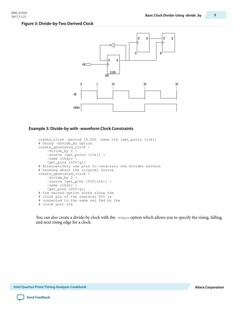
Figure 3: Divide-by-Two Derived Clock
A
clk
B
D Q D Q
clk
0 5 10 20 30
clkdiv
DIVCLRN
D Q
Example 3: Divide-by with -waveform Clock Constraints
create_clock -period 10.000 -name clk [get_ports {clk}]# Using -divide_by optioncreate_generated_clock \ -divide_by 2 \ -source [get_ports {clk}] \ -name clkdiv \ [get_pins {DIV|q}]# Alternatively use pins to constrain the divider without# knowing about the original sourcecreate_generated_clock \ -divide_by 2 \ -source [get_pins {DIV|clk}] \ -name clkdiv \ [get_pins {DIV|q}]# the second option works since the# clock pin of the register DIV is# connected to the same net fed by the# clock port clk
You can also create a divide-by clock with the -edges option which allows you to specify the rising, falling,and next rising edge for a clock.
MNL-010352017.11.21 Basic Clock Divider Using -divide_by 3
Intel Quartus Prime Timing Analyzer Cookbook Altera Corporation
Send Feedback
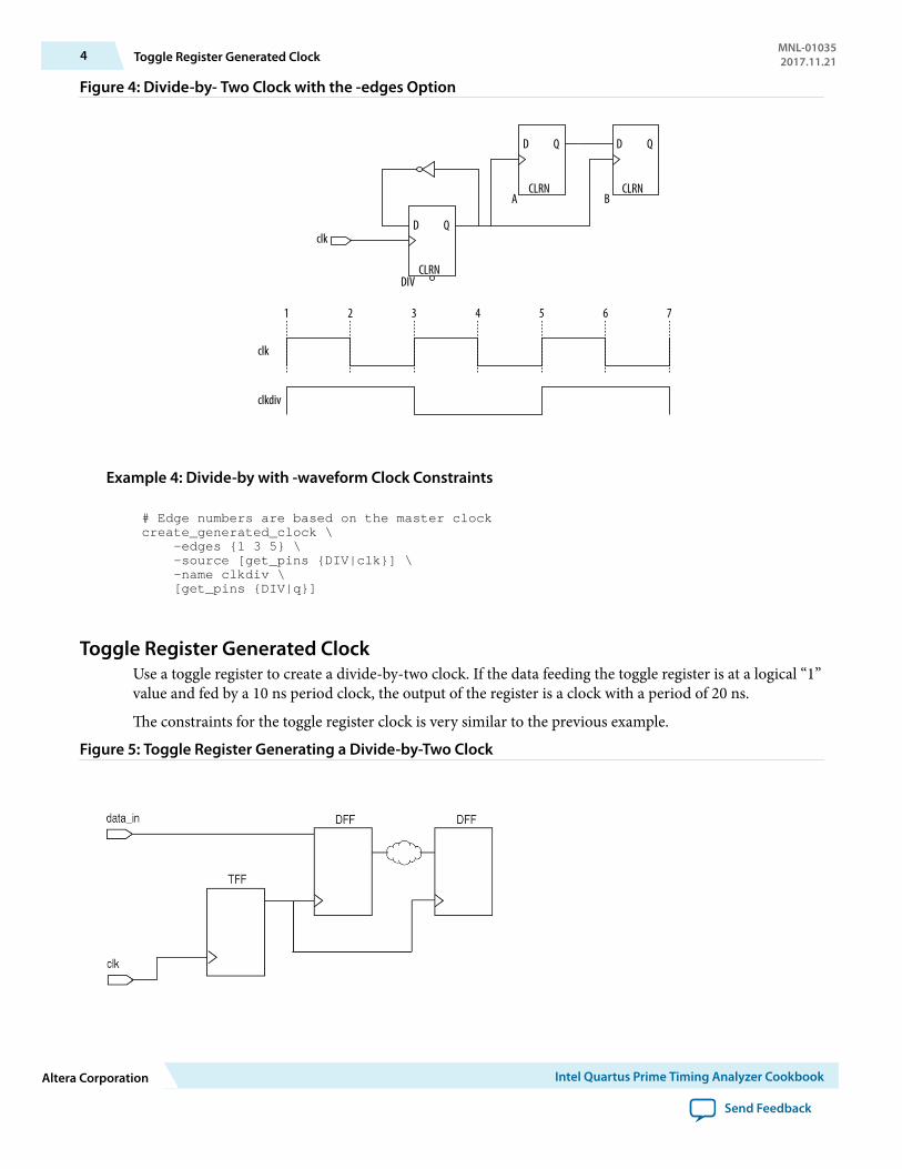
Figure 4: Divide-by- Two Clock with the -edges Option
CLRNA
clk
B
D Q
CLRN
D Q
1 2 3 5 74 6
clkdiv
DIVCLRN
D Q
clk
Example 4: Divide-by with -waveform Clock Constraints
# Edge numbers are based on the master clockcreate_generated_clock \ -edges {1 3 5} \ -source [get_pins {DIV|clk}] \ -name clkdiv \ [get_pins {DIV|q}]
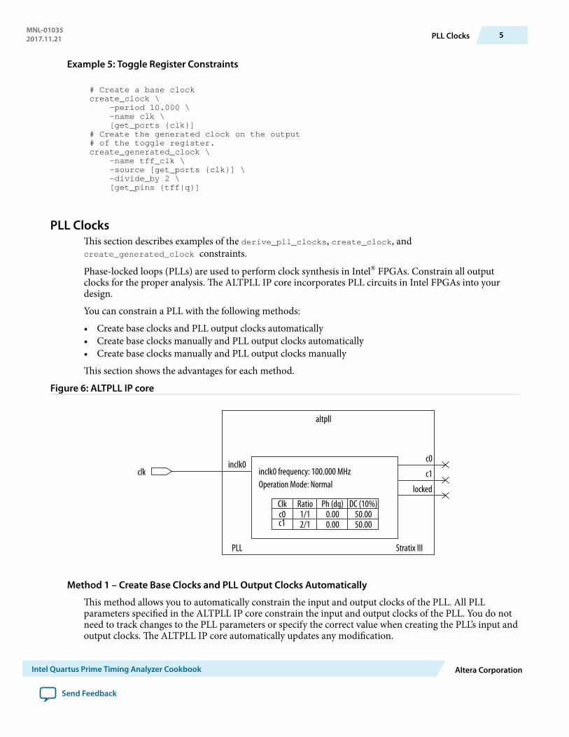
Toggle Register Generated ClockUse a toggle register to create a divide-by-two clock. If the data feeding the toggle register is at a logical “1”value and fed by a 10 ns period clock, the output of the register is a clock with a period of 20 ns.
The constraints for the toggle register clock is very similar to the previous example.
Figure 5: Toggle Register Generating a Divide-by-Two Clock
4 Toggle Register Generated ClockMNL-010352017.11.21
Altera Corporation Intel Quartus Prime Timing Analyzer Cookbook
Send Feedback
Example 5: Toggle Register Constraints
# Create a base clockcreate_clock \ -period 10.000 \ -name clk \ [get_ports {clk}]# Create the generated clock on the output# of the toggle register.create_generated_clock \ -name tff_clk \ -source [get_ports {clk}] \ -divide_by 2 \ [get_pins {tff|q}]
PLL ClocksThis section describes examples of the derive_pll_clocks, create_clock, andcreate_generated_clock constraints.
Phase-locked loops (PLLs) are used to perform clock synthesis in Intel® FPGAs. Constrain all outputclocks for the proper analysis. The ALTPLL IP core incorporates PLL circuits in Intel FPGAs into yourdesign.
You can constrain a PLL with the following methods:
• Create base clocks and PLL output clocks automatically• Create base clocks manually and PLL output clocks automatically• Create base clocks manually and PLL output clocks manually
This section shows the advantages for each method.
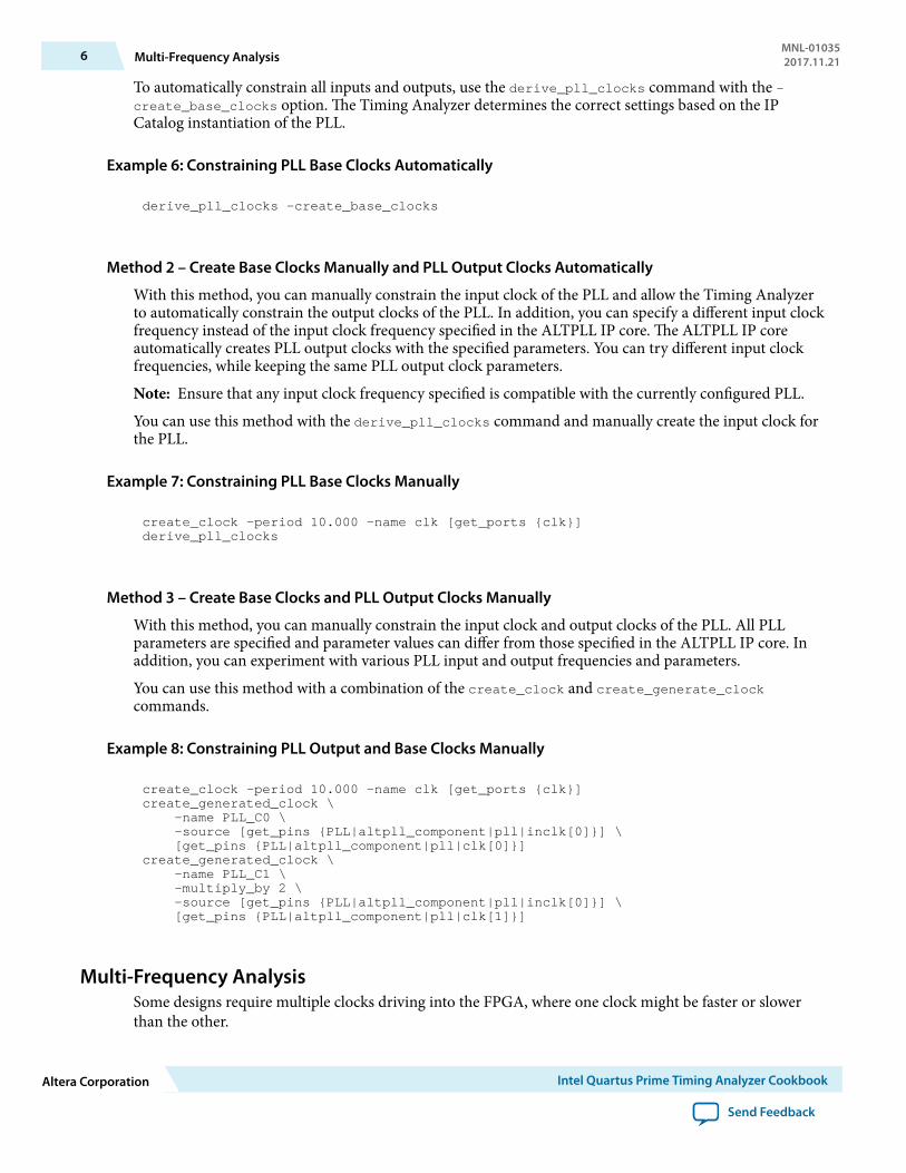
Figure 6: ALTPLL IP core
clk
Clk
Operation Mode: Normalinclk0 frequency: 100.000 MHz
altpll
inclk0
locked
Stratix III
c1
c0
PLL
c0c1
1/12/1
0.000.00
50.0050.00
Ratio Ph (dg) DC (10%)
Method 1 – Create Base Clocks and PLL Output Clocks Automatically
This method allows you to automatically constrain the input and output clocks of the PLL. All PLLparameters specified in the ALTPLL IP core constrain the input and output clocks of the PLL. You do notneed to track changes to the PLL parameters or specify the correct value when creating the PLL’s input andoutput clocks. The ALTPLL IP core automatically updates any modification.
MNL-010352017.11.21 PLL Clocks 5
Intel Quartus Prime Timing Analyzer Cookbook Altera Corporation
Send Feedback
To automatically constrain all inputs and outputs, use the derive_pll_clocks command with the -create_base_clocks option. The Timing Analyzer determines the correct settings based on the IPCatalog instantiation of the PLL.
Example 6: Constraining PLL Base Clocks Automatically
derive_pll_clocks -create_base_clocks
Method 2 – Create Base Clocks Manually and PLL Output Clocks Automatically
With this method, you can manually constrain the input clock of the PLL and allow the Timing Analyzerto automatically constrain the output clocks of the PLL. In addition, you can specify a different input clockfrequency instead of the input clock frequency specified in the ALTPLL IP core. The ALTPLL IP coreautomatically creates PLL output clocks with the specified parameters. You can try different input clockfrequencies, while keeping the same PLL output clock parameters.
Note: Ensure that any input clock frequency specified is compatible with the currently configured PLL.
You can use this method with the derive_pll_clocks command and manually create the input clock forthe PLL.
Example 7: Constraining PLL Base Clocks Manually
create_clock -period 10.000 -name clk [get_ports {clk}]derive_pll_clocks
Method 3 – Create Base Clocks and PLL Output Clocks Manually
With this method, you can manually constrain the input clock and output clocks of the PLL. All PLLparameters are specified and parameter values can differ from those specified in the ALTPLL IP core. Inaddition, you can experiment with various PLL input and output frequencies and parameters.
You can use this method with a combination of the create_clock and create_generate_clockcommands.
Example 8: Constraining PLL Output and Base Clocks Manually
create_clock -period 10.000 -name clk [get_ports {clk}]create_generated_clock \ -name PLL_C0 \ -source [get_pins {PLL|altpll_component|pll|inclk[0]}] \ [get_pins {PLL|altpll_component|pll|clk[0]}]create_generated_clock \ -name PLL_C1 \ -multiply_by 2 \ -source [get_pins {PLL|altpll_component|pll|inclk[0]}] \ [get_pins {PLL|altpll_component|pll|clk[1]}]
Multi-Frequency AnalysisSome designs require multiple clocks driving into the FPGA, where one clock might be faster or slowerthan the other.
6 Multi-Frequency AnalysisMNL-010352017.11.21
Altera Corporation Intel Quartus Prime Timing Analyzer Cookbook
Send Feedback
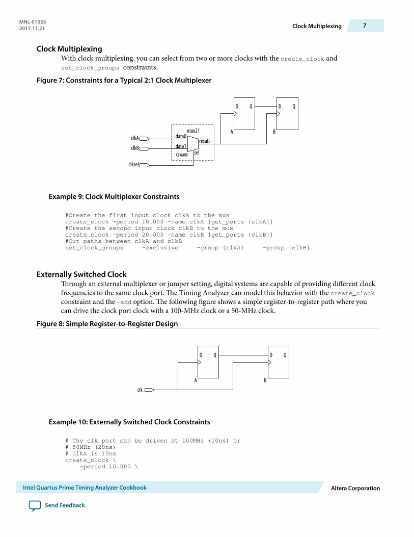
Clock MultiplexingWith clock multiplexing, you can select from two or more clocks with the create_clock andset_clock_groups constraints.
Figure 7: Constraints for a Typical 2:1 Clock Multiplexer
A
clksel
B
D Q
mux21
CLKMUX
D Q
clkA
clkB data1sel
data0result
Example 9: Clock Multiplexer Constraints
#Create the first input clock clkA to the muxcreate_clock -period 10.000 -name clkA [get_ports {clkA}]#Create the second input clock clkB to the muxcreate_clock -period 20.000 -name clkB [get_ports {clkB}]#Cut paths between clkA and clkBset_clock_groups -exclusive -group {clkA} -group {clkB}
Externally Switched ClockThrough an external multiplexer or jumper setting, digital systems are capable of providing different clockfrequencies to the same clock port. The Timing Analyzer can model this behavior with the create_clockconstraint and the -add option. The following figure shows a simple register-to-register path where youcan drive the clock port clock with a 100-MHz clock or a 50-MHz clock.
Figure 8: Simple Register-to-Register Design
A
clk
B
D Q D Q
Example 10: Externally Switched Clock Constraints
# The clk port can be driven at 100MHz (10ns) or# 50MHz (20ns)# clkA is 10nscreate_clock \ -period 10.000 \
MNL-010352017.11.21 Clock Multiplexing 7
Intel Quartus Prime Timing Analyzer Cookbook Altera Corporation
Send Feedback
-name clkA \ [get_ports {clk}]# clkB is 20ns assigned to the same port# Requires -add optioncreate_clock \ -period 20.000 \ -name clkB \ [get_ports {clk}] \ -addset_clock_groups \ -exclusive \ -group {clkA} \ -group {clkB}
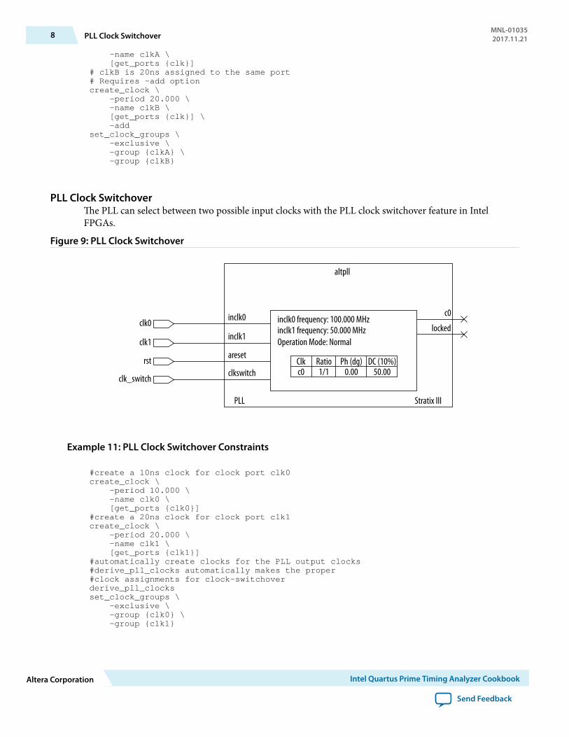
PLL Clock SwitchoverThe PLL can select between two possible input clocks with the PLL clock switchover feature in IntelFPGAs.
Figure 9: PLL Clock Switchover
clk0
Clk
Operation Mode: Normal
inclk0 frequency: 100.000 MHzinclk1 frequency: 50.000 MHz
altpll
inclk0locked
Stratix III
c0
PLL
c0 1/1 0.00 50.00Ratio Ph (dg) DC (10%)
clk1 inclk1
rst areset
clk_switch clkswitch
Example 11: PLL Clock Switchover Constraints
#create a 10ns clock for clock port clk0create_clock \ -period 10.000 \ -name clk0 \ [get_ports {clk0}]#create a 20ns clock for clock port clk1create_clock \ -period 20.000 \ -name clk1 \ [get_ports {clk1}]#automatically create clocks for the PLL output clocks#derive_pll_clocks automatically makes the proper#clock assignments for clock-switchoverderive_pll_clocksset_clock_groups \ -exclusive \ -group {clk0} \ -group {clk1}
8 PLL Clock SwitchoverMNL-010352017.11.21
Altera Corporation Intel Quartus Prime Timing Analyzer Cookbook
Send Feedback
I/O Constraints
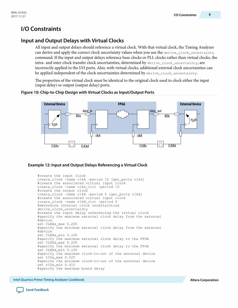
Input and Output Delays with Virtual ClocksAll input and output delays should reference a virtual clock. With that virtual clock, the Timing Analyzercan derive and apply the correct clock uncertainty values when you use the derive_clock_uncertaintycommand. If the input and output delays reference base clocks or PLL clocks rather than virtual clocks, theintra- and inter-clock transfer clock uncertainties, determined by derive_clock_uncertainty, areincorrectly applied to the I/O ports. Also, with virtual clocks, additional external clock uncertainties canbe applied independent of the clock uncertainties determined by derive_clock_uncertainty.
The properties of the virtual clock must be identical to the original clock used to clock either the input(input delay) or output (output delay) ports.
Figure 10: Chip-to-Chip Design with Virtual Clocks as Input/Output Ports
External Device External DeviceFPGA
BDa BDb
clkA
tCOatSUb
data_in
CLKAdCLKAs
clkB
CLKBs CLKBd
data_out
Example 12: Input and Output Delays Referencing a Virtual Clock
#create the input clockcreate_clock -name clkA -period 10 [get_ports clkA]#create the associated virtual input clockcreate_clock -name clkA_virt -period 10#create the output clockcreate_clock -name clkB -period 5 [get_ports clkB]#create the associated virtual input clockcreate_clock -name clkB_virt -period 5#determine internal clock uncertaintiesderive_clock_uncertainty#create the input delay referencing the virtual clock#specify the maximum external clock delay from the external#deviceset CLKAs_max 0.200#specify the minimum external clock delay from the external#deviceset CLKAs_min 0.100#specify the maximum external clock delay to the FPGAset CLKAd_max 0.200#specify the minimum external clock delay to the FPGAset CLKAd_min 0.100#specify the maximum clock-to-out of the external deviceset tCOa_max 0.525#specify the minimum clock-to-out of the external deviceset tCOa_min 0.415#specify the maximum board delay
MNL-010352017.11.21 I/O Constraints 9
Intel Quartus Prime Timing Analyzer Cookbook Altera Corporation
Send Feedback
set BDa_max 0.180#specify the minimum board delayset BDa_min 0.120#create the input maximum delay for the data input to the#FPGA that accounts for all delays specifiedset_input_delay -clock clkA_virt \-max [expr $CLKAs_max + $tCOa_max + $BDa_max - $CLKAd_min] \[get_ports {data_in[*]}]#create the input minimum delay for the data input to the#FPGA that accounts for all delays specifiedset_input_delay -clock clkA_virt \-min [expr $CLKAs_min + $tCOa_min + $BDa_min - $CLKAd_max] \[get_ports {data_in[*]}]#creating the output delay referencing the virtual clock#specify the maximum external clock delay to the FPGAset CLKBs_max 0.100#specify the minimum external clock delay to the FPGAset CLKBs_min 0.050#specify the maximum external clock delay to the external deviceset CLKBd_max 0.100#specify the minimum external clock delay to the external deviceset CLKBd_min 0.050#specify the maximum setup time of the external deviceset tSUb 0.500#specify the hold time of the external deviceset tHb 0.400#specify the maximum board delayset BDb_max 0.100#specify the minimum board delayset BDb_min 0.080#create the output maximum delay for the data output from the#FPGA that accounts for all delays specifiedset_output_delay -clock clkB_virt \-max [expr $CLKBs_max + $tSUb + $BDb_max - $CLKBd_min] \[get_ports {data_out}]#create the output minimum delay for the data output from the#FPGA that accounts for all delays specifiedset_output_delay -clock clkB_virt \-min [expr $CLKBs_min - $tHb + $BDb_min - $CLKBd_max] \[get_ports {data_out}]
Tri-State OutputsTri-state outputs allow either a valid data signal or a high impedance signal to be driven out of an outputor I/O port. The timing of either signal is important in the overall system timing of the design.
The timing constraints for tri-state outputs are identical to regular output ports.
10 Tri-State OutputsMNL-010352017.11.21
Altera Corporation Intel Quartus Prime Timing Analyzer Cookbook
Send Feedback
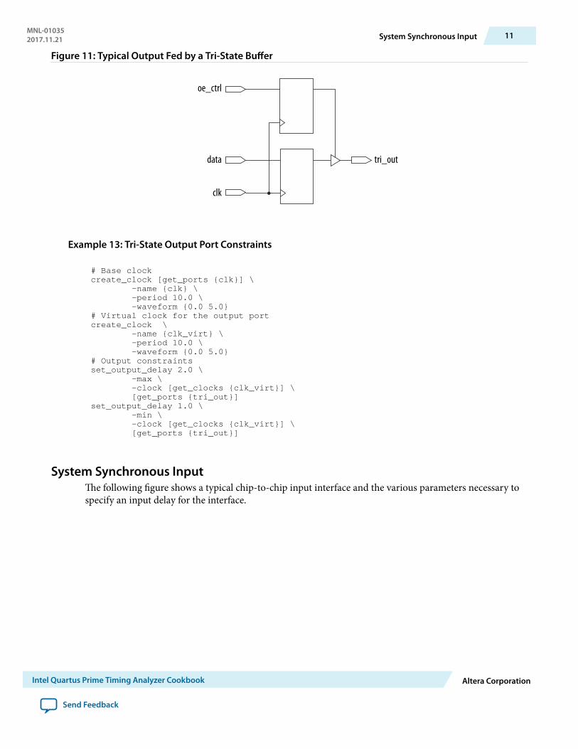
Figure 11: Typical Output Fed by a Tri-State Buffer
oe_ctrl
data
clk
tri_out
Example 13: Tri-State Output Port Constraints
# Base clockcreate_clock [get_ports {clk}] \ -name {clk} \ -period 10.0 \ -waveform {0.0 5.0}# Virtual clock for the output portcreate_clock \ -name {clk_virt} \ -period 10.0 \ -waveform {0.0 5.0}# Output constraintsset_output_delay 2.0 \ -max \ -clock [get_clocks {clk_virt}] \ [get_ports {tri_out}]set_output_delay 1.0 \ -min \ -clock [get_clocks {clk_virt}] \ [get_ports {tri_out}]
System Synchronous InputThe following figure shows a typical chip-to-chip input interface and the various parameters necessary tospecify an input delay for the interface.
MNL-010352017.11.21 System Synchronous Input 11
Intel Quartus Prime Timing Analyzer Cookbook Altera Corporation
Send Feedback
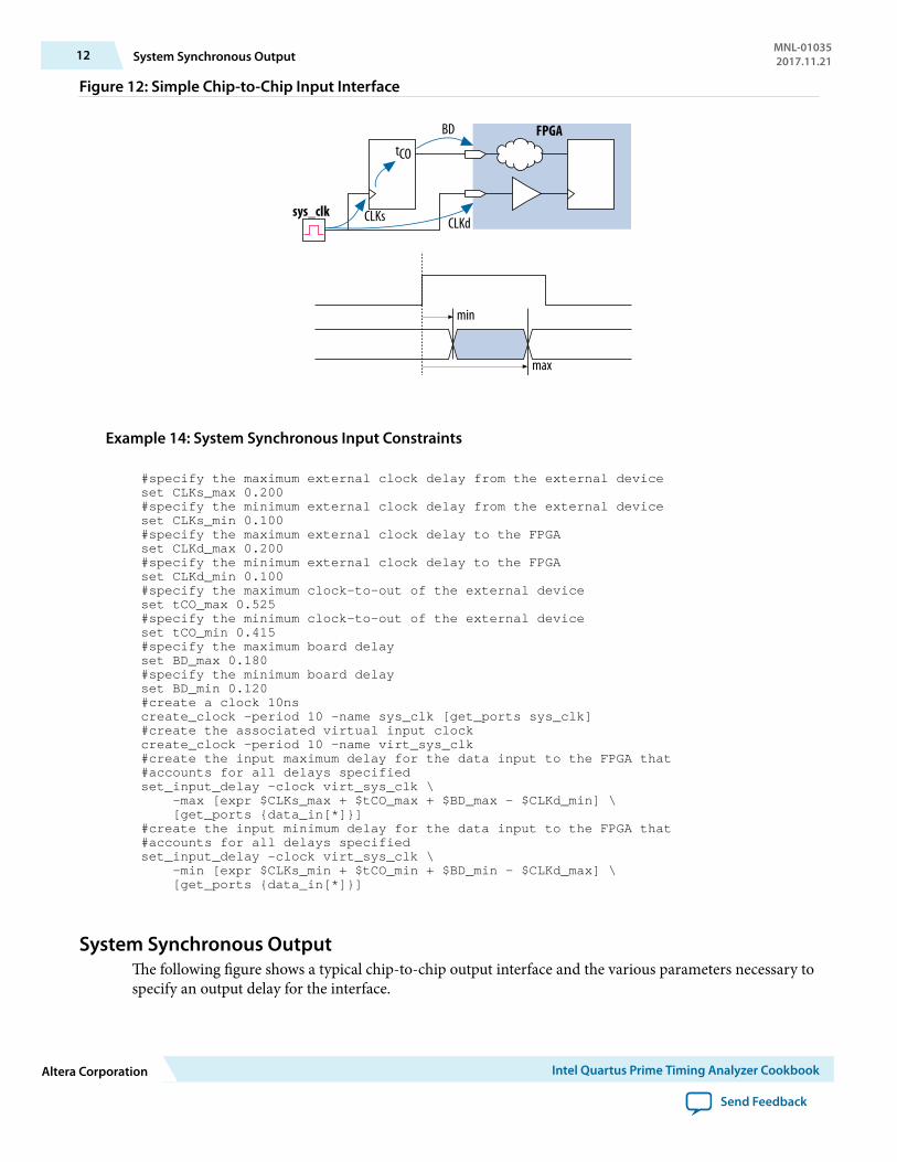
Figure 12: Simple Chip-to-Chip Input Interface
min
max
tCO
CLKs CLKd
BD FPGA
sys_clk
Example 14: System Synchronous Input Constraints
#specify the maximum external clock delay from the external deviceset CLKs_max 0.200#specify the minimum external clock delay from the external deviceset CLKs_min 0.100#specify the maximum external clock delay to the FPGAset CLKd_max 0.200#specify the minimum external clock delay to the FPGAset CLKd_min 0.100#specify the maximum clock-to-out of the external deviceset tCO_max 0.525#specify the minimum clock-to-out of the external deviceset tCO_min 0.415#specify the maximum board delayset BD_max 0.180#specify the minimum board delayset BD_min 0.120#create a clock 10nscreate_clock -period 10 -name sys_clk [get_ports sys_clk]#create the associated virtual input clockcreate_clock -period 10 -name virt_sys_clk#create the input maximum delay for the data input to the FPGA that #accounts for all delays specifiedset_input_delay -clock virt_sys_clk \ -max [expr $CLKs_max + $tCO_max + $BD_max - $CLKd_min] \ [get_ports {data_in[*]}]#create the input minimum delay for the data input to the FPGA that #accounts for all delays specifiedset_input_delay -clock virt_sys_clk \ -min [expr $CLKs_min + $tCO_min + $BD_min - $CLKd_max] \ [get_ports {data_in[*]}]
System Synchronous OutputThe following figure shows a typical chip-to-chip output interface and the various parameters necessary tospecify an output delay for the interface.
12 System Synchronous OutputMNL-010352017.11.21
Altera Corporation Intel Quartus Prime Timing Analyzer Cookbook
Send Feedback
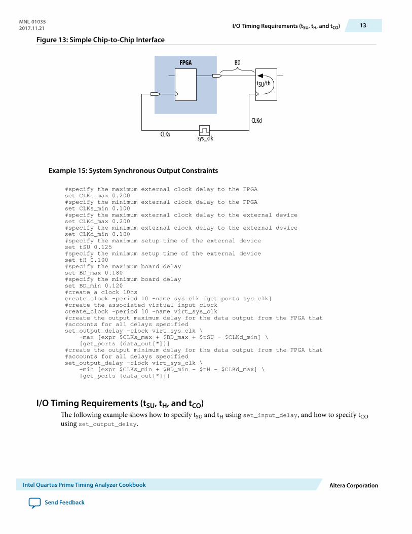
Figure 13: Simple Chip-to-Chip Interface
FPGA
CLKd
sys_clkCLKs
BD
tSU/th
Example 15: System Synchronous Output Constraints
#specify the maximum external clock delay to the FPGAset CLKs_max 0.200#specify the minimum external clock delay to the FPGAset CLKs_min 0.100#specify the maximum external clock delay to the external deviceset CLKd_max 0.200#specify the minimum external clock delay to the external deviceset CLKd_min 0.100#specify the maximum setup time of the external deviceset tSU 0.125#specify the minimum setup time of the external deviceset tH 0.100#specify the maximum board delayset BD_max 0.180#specify the minimum board delayset BD_min 0.120#create a clock 10nscreate_clock -period 10 -name sys_clk [get_ports sys_clk]#create the associated virtual input clockcreate_clock -period 10 -name virt_sys_clk#create the output maximum delay for the data output from the FPGA that #accounts for all delays specifiedset_output_delay -clock virt_sys_clk \ -max [expr $CLKs_max + $BD_max + $tSU - $CLKd_min] \ [get_ports {data_out[*]}]#create the output minimum delay for the data output from the FPGA that #accounts for all delays specifiedset_output_delay -clock virt_sys_clk \ -min [expr $CLKs_min + $BD_min - $tH - $CLKd_max] \ [get_ports {data_out[*]}]
I/O Timing Requirements (tSU, tH, and tCO)The following example shows how to specify tSU and tH using set_input_delay, and how to specify tCOusing set_output_delay.
MNL-010352017.11.21 I/O Timing Requirements (tSU, tH, and tCO) 13
Intel Quartus Prime Timing Analyzer Cookbook Altera Corporation
Send Feedback
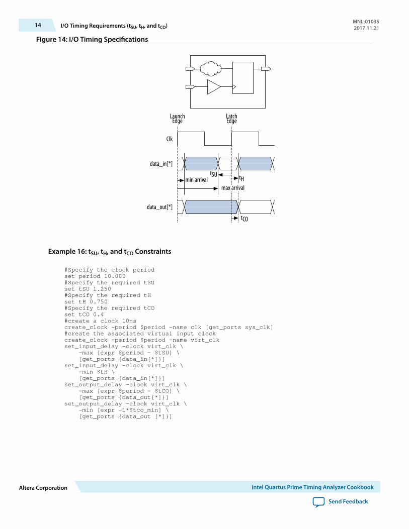
Figure 14: I/O Timing Specifications
LaunchEdge
LatchEdge
data_in[*]
Clk
min arrival tHtSU
max arrival
data_out[*]
tCO
Example 16: tSU, tH, and tCO Constraints
#Specify the clock periodset period 10.000#Specify the required tSUset tSU 1.250#Specify the required tHset tH 0.750#Specify the required tCOset tCO 0.4#create a clock 10nscreate_clock -period $period -name clk [get_ports sys_clk]#create the associated virtual input clockcreate_clock -period $period -name virt_clkset_input_delay -clock virt_clk \ -max [expr $period - $tSU] \ [get_ports {data_in[*]}]set_input_delay -clock virt_clk \ -min $tH \ [get_ports {data_in[*]}]set_output_delay -clock virt_clk \ -max [expr $period - $tCO] \ [get_ports {data_out[*]}]set_output_delay -clock virt_clk \ -min [expr -1*$tco_min] \ [get_ports {data_out [*]}]
14 I/O Timing Requirements (tSU, tH, and tCO)MNL-010352017.11.21
Altera Corporation Intel Quartus Prime Timing Analyzer Cookbook
Send Feedback
Exceptions
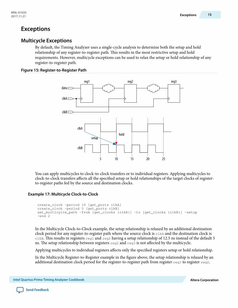
Multicycle ExceptionsBy default, the Timing Analyzer uses a single-cycle analysis to determine both the setup and holdrelationship of any register-to-register path. This results in the most restrictive setup and holdrequirements. However, multicycle exceptions can be used to relax the setup or hold relationship of anyregister-to-register path.
Figure 15: Register-to-Register Path
data
clkA
clkB
clkA
5 10 15 20 25
clkB
reg1 reg2 reg3
setuphold
You can apply multicycles to clock-to-clock transfers or to individual registers. Applying multicycles toclock-to-clock transfers affects all the specified setup or hold relationships of the target clocks of register-to-register paths fed by the source and destination clocks.
Example 17: Multicycle Clock-to-Clock
create_clock -period 10 [get_ports clkA]create_clock -period 5 [get_ports clkB]set_multicycle_path -from [get_clocks {clkA}] -to [get_clocks {clkB}] -setup -end 2
In the Multicycle Clock-to-Clock example, the setup relationship is relaxed by an additional destinationclock period for any register-to-register path where the source clock is clkA and the destination clock isclkB. This results in registers reg1 and reg2 having a setup relationship of 12.5 ns instead of the default 5ns. The setup relationship between registers reg2 and reg3 is not affected by the multicycle.
Applying multicycles to individual registers affects only the specified registers setup or hold relationship.
In the Multicycle Register-to-Register example in the figure above, the setup relationship is relaxed by anadditional destination clock period for the register-to-register path from register reg1 to register reg2.
MNL-010352017.11.21 Exceptions 15
Intel Quartus Prime Timing Analyzer Cookbook Altera Corporation
Send Feedback
This results in registers reg1 and reg2 having a setup relationship of 10 ns instead of the default 5 ns. Thesetup relationship between registers reg2 and reg3 is not affected by the multicycle.
Example 18: Multicycle Register-to-Register
create_clock -period 10 [get_ports clkA]create_clock -period 5 [get_ports clkB]set_multicycle_path -from [get_pins {reg1|q}] -to [get_pins {reg2|d}] -setup -end 2
Related InformationThe Intel Quartus® Prime Timing AnalyzerFor more information about the types of multicycle exceptions available in the Timing Analyzer.
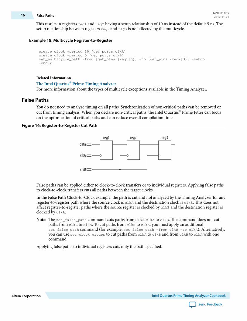
False PathsYou do not need to analyze timing on all paths. Synchronization of non-critical paths can be removed orcut from timing analysis. When you declare non-critical paths, the Intel Quartus® Prime Fitter can focuson the optimization of critical paths and can reduce overall compilation time.
Figure 16: Register-to-Register Cut Path
data
clkA
clkB
reg1 reg2 reg3
False paths can be applied either to clock-to-clock transfers or to individual registers. Applying false pathsto clock-to-clock transfers cuts all paths between the target clocks.
In the False Path Clock-to-Clock example, the path is cut and not analyzed by the Timing Analyzer for anyregister-to-register path where the source clock is clkA and the destination clock is clkB. This does notaffect register-to-register paths where the source register is clocked by clkB and the destination register isclocked by clkA.
Note: The set_false_path command cuts paths from clock clkA to clkB. The command does not cutpaths from clkB to clkA. To cut paths from clkB to clkA, you must apply an additionalset_false_path command (for example, set_false_path -from clkB -to clkA). Alternatively,you can use set_clock_groups to cut paths from clkA to clkB and from clkB to clkA with onecommand.
Applying false paths to individual registers cuts only the path specified.
16 False PathsMNL-010352017.11.21
Altera Corporation Intel Quartus Prime Timing Analyzer Cookbook
Send Feedback
Example 19: False Path Clock-to-Clock
create_clock -period 12 [get_ports clkA]create_clock -period 5 [get_ports clkB]set_false_path -from [get_clocks {clkA}] -to [get_clocks {clkB}]
In the False Path Register-to-Register example, the register-to-register path from register reg1 to registerreg2 is cut. All other paths remain unaffected.
Example 20: False Path Register-to-Register
create_clock -period 10 [get_ports clkA]create_clock -period 5 [get_ports clkB]set_false_path -from [get_pins {reg1|q}] -to [get_pins {reg2|d}]
Related InformationSet Clock Groups Dialog Box (set_clock_groups)For more information about the set_clock_groups command in Intel Quartus Prime Help.
Miscellaneous
JTAG SignalsMany in-system debugging tools use the JTAG interface in Intel FPGAs.
When you debug your design with the JTAG interface, the JTAG signals TCK, TMS, TDI, and TDO areimplemented as part of the design. Because of this, the Timing Analyzer flags these signals asunconstrained when an unconstrained path report is generated.
Table 1: JTAG Signals That Might Appear as Unconstrained
Signal Name Description
altera_reserved_tck(1) (2) JTAG test clock input portaltera_reserved_tms(2) JTAG test mode select input portaltera_reserved_tdi(2) JTAG test data input line input portaltera_reserved_tdo(2) JTAG test data output line output port
(1) Constrained under Intel Quartus Prime Standard Edition by default.(2) Unconstrained under Intel Quartus Prime Pro Edition unless you use a variation of the SDC example
contained in the JTAG Signal Constraints template.
MNL-010352017.11.21 Miscellaneous 17
Intel Quartus Prime Timing Analyzer Cookbook Altera Corporation
Send Feedback
You can constrain the JTAG signals by applying the following SDC commands:
Example 21: JTAG Signal Constraints
# Search "---customize here---" for the few decisions you need to make ## By default, the most challenging timing spec is applied to work in # many JTAG chain setup situations
set_time_format -unit ns -decimal_places 3
# This is the main entry point called at the end of this SDC file.proc set_jtag_timing_constraints { } { # If the timing characteristic outside of FPGA is well understood, and # there is a need to provide more slack to allow flexible placement of # JTAG logic in the FPGA core, use the timing constraints for both # timing analysis and fitter; otherwise, use the default fitter timing # constraints.
# ---customize here--- set use_fitter_specific_constraint 1
if { $use_fitter_specific_constraint && [string equal quartus_fit $::TimeQuestInfo(nameofexecutable)] } { # Define a different set of timing spec to influence place-and-route # result in the jtag clock domain. The slacks outside of FPGA are # maximized.
set_default_quartus_fit_timing_directive } else { # Define a set of timing constraints that describe the JTAG paths # for the Timing Analyzer to analyze. The Timing Analyzer timing reports show whether # the JTAG logic in the FPGA core will operates in this setup.
set_jtag_timing_spec_for_timing_analysis }}
proc set_default_quartus_fit_timing_directive { } { # A10 supports max 33.3Mhz clock set jtag_33Mhz_t_period 30
create_clock -name {altera_reserved_tck} -period $jtag_33Mhz_t_period [get_ports {altera_reserved_tck}] set_clock_groups -asynchronous -group {altera_reserved_tck} # Force fitter to place register driving TDO pin to be as close to # the JTAG controller as possible to maximize the slack outside of FPGA. set_max_delay -to [get_ports { altera_reserved_tdo } ] 0 }
proc set_jtag_timing_spec_for_timing_analysis { } {derive_clock_uncertainty
# There are few possible JTAG chain configurations: # a. This device is the only device in the JTAG chain # b. This device is the first one in the JTAG chain # c. This device is in the middle of the JTAG chain # d. This device is the last one in the JTAG chain
# No matter where the device is in the chain. The tck and tms are driven # directly from JTAG hardware. set_tck_timing_spec set_tms_timing_spec
18 JTAG SignalsMNL-010352017.11.21
Altera Corporation Intel Quartus Prime Timing Analyzer Cookbook
Send Feedback
# Depending on where the device is located along the chain, tdi can be # either driven by blaster hw (a. b.) or driven by another device in the # chain(c. d.) # ---customize here--- set tdi_is_driven_by_blaster 1
if { $tdi_is_driven_by_blaster } { set_tdi_timing_spec_when_driven_by_blaster } else { set_tdi_timing_spec_when_driven_by_device }
# Depending on where the device is located along the chain, tdo can # drive either blaster hw (a. d.) or another device in the chain (b. c.) # ---customize here--- set tdo_drive_blaster 1
if { $tdo_drive_blaster } { set_tdo_timing_spec_when_drive_blaster } else { set_tdo_timing_spec_when_drive_device }
set_optional_ntrst_timing_spec
# Cut a few timing paths that are not related to JTAG logic in # the FPGA core, such as security mode. set_false_path -from [get_ports {altera_reserved_tdi}] -to [get_ports {altera_reserved_tdo}] if { [get_collection_size [get_registers -nowarn *~jtag_reg]] > 0 } { set_false_path -from [get_registers *~jtag_reg] -to [get_ports {altera_reserved_tdo}] }
}
proc set_tck_timing_spec { } { # USB Blaster 1 uses 6 MHz clock = 166.666 ns period set ub1_t_period 166.666 # USB Blaster 2 uses 24 MHz clock = 41.666 ns period set ub2_default_t_period 41.666 # USB Blaster 2 running at 16 MHz clock safe mode = 62.5 ns period set ub2_safe_t_period 62.5
# ---customize here--- set tck_t_period $ub2_default_t_period
create_clock -name {altera_reserved_tck} -period $tck_t_period [get_ports {altera_reserved_tck}] set_clock_groups -asynchronous -group {altera_reserved_tck}}
proc get_tck_delay_max { } { set tck_blaster_tco_max 14.603 set tck_cable_max 11.627
# tck delay on the PCB depends on the trace length from JTAG 10-pin # header to FPGA on board. In general on the PCB, the signal travels # at the speed of ~160 ps/inch (1000 mils = 1 inch). # ---customize here--- set tck_header_trace_max 0.5
return [expr $tck_blaster_tco_max + $tck_cable_max + $tck_header_trace_max]}
proc get_tck_delay_min { } {
MNL-010352017.11.21 JTAG Signals 19
Intel Quartus Prime Timing Analyzer Cookbook Altera Corporation
Send Feedback
set tck_blaster_tco_min 14.603 set tck_cable_min 10.00
# tck delay on the PCB depends on the trace length from JTAG 10-pin # header to FPGA on board. In general on the PCB, the signal travels # at the speed of ~160 ps/inch (1000 mils = 1 inch). # ---customize here--- set tck_header_trace_min 0.1
return [expr $tck_blaster_tco_min + $tck_cable_min + $tck_header_trace_min]}
proc set_tms_timing_spec { } { set tms_blaster_tco_max 9.468 set tms_blaster_tco_min 9.468
set tms_cable_max 11.627 set tms_cable_min 10.0
# tms delay on the PCB depends on the trace length from JTAG 10-pin # header to FPGA on board. In general on the PCB, the signal travels # at the speed of ~160 ps/inch (1000 mils = 1 inch). # ---customize here--- set tms_header_trace_max 0.5 set tms_header_trace_min 0.1
set tms_in_max [expr $tms_cable_max + $tms_header_trace_max + $tms_blaster_tco_max - [get_tck_delay_min]] set tms_in_min [expr $tms_cable_min + $tms_header_trace_min + $tms_blaster_tco_min - [get_tck_delay_max]]
set_input_delay -add_delay -clock_fall -clock altera_reserved_tck -max $tms_in_max [get_ports {altera_reserved_tms}] set_input_delay -add_delay -clock_fall -clock altera_reserved_tck -min $tms_in_min [get_ports {altera_reserved_tms}]}
proc set_tdi_timing_spec_when_driven_by_blaster { } { set tdi_blaster_tco_max 8.551 set tdi_blaster_tco_min 8.551
set tdi_cable_max 11.627 set tdi_cable_min 10.0
# tms delay on the PCB depends on the trace length from JTAG 10-pin # header to FPGA on board. In general on the PCB, the signal travels # at the speed of ~160 ps/inch (1000 mils = 1 inch). # ---customize here--- set tdi_header_trace_max 0.5 set tdi_header_trace_min 0.1
set tdi_in_max [expr $tdi_cable_max + $tdi_header_trace_max + $tdi_blaster_tco_max - [get_tck_delay_min]] set tdi_in_min [expr $tdi_cable_min + $tdi_header_trace_min + $tdi_blaster_tco_min - [get_tck_delay_max]]
#TDI launches at the falling edge of TCK per standard set_input_delay -add_delay -clock_fall -clock altera_reserved_tck -max $tdi_in_max [get_ports {altera_reserved_tdi}] set_input_delay -add_delay -clock_fall -clock altera_reserved_tck -min $tdi_in_min [get_ports {altera_reserved_tdi}]}
proc set_tdi_timing_spec_when_driven_by_device { } { # TCO timing spec of tdo on the device driving this tdi input # ---customize here---
20 JTAG SignalsMNL-010352017.11.21
Altera Corporation Intel Quartus Prime Timing Analyzer Cookbook
Send Feedback
set previous_device_tdo_tco_max 10.0 set previous_device_tdo_tco_min 10.0
# tdi delay on the PCB depends on the trace length from JTAG 10-pin # header to FPGA on board. In general on the PCB, the signal travels # at the speed of ~160 ps/inch (1000 mils = 1 inch). # ---customize here--- set tdi_trace_max 0.5 set tdi_trace_min 0.1
set tdi_in_max [expr $previous_device_tdo_tco_max + $tdi_trace_max - [get_tck_delay_min]] set tdi_in_min [expr $previous_device_tdo_tco_min + $tdi_trace_min - [get_tck_delay_max]]
#TDI launches at the falling edge of TCK per standard set_input_delay -add_delay -clock_fall -clock altera_reserved_tck -max $tdi_in_max [get_ports {altera_reserved_tdi}] set_input_delay -add_delay -clock_fall -clock altera_reserved_tck -min $tdi_in_min [get_ports {altera_reserved_tdi}]}
proc set_tdo_timing_spec_when_drive_blaster { } { set tdo_blaster_tsu 5.831 set tdo_blaster_th -1.651
set tdo_cable_max 11.627 set tdo_cable_min 10.0
# tdi delay on the PCB depends on the trace length from JTAG 10-pin # header to FPGA on board. In general on the PCB, the signal travels # at the speed of ~160 ps/inch (1000 mils = 1 inch). # ---customize here--- set tdo_header_trace_max 0.5 set tdo_header_trace_min 0.1
set tdo_out_max [expr $tdo_cable_max + $tdo_header_trace_max + $tdo_blaster_tsu + [get_tck_delay_max]] set tdo_out_min [expr $tdo_cable_min + $tdo_header_trace_min - $tdo_blaster_th + [get_tck_delay_min]]
#TDO does not latch inside the USB Blaster II at the rising edge of TCK, # it actually is latched one half cycle later in packed mode # (equivalent to 1 JTAG fall-to-fall cycles) set_output_delay -add_delay -clock_fall -clock altera_reserved_tck -max $tdo_out_max [get_ports {altera_reserved_tdo}] set_output_delay -add_delay -clock_fall -clock altera_reserved_tck -min $tdo_out_min [get_ports {altera_reserved_tdo}]}
proc set_tdo_timing_spec_when_drive_device { } { # TCO timing spec of tdi on the device driven by this tdo output # ---customize here--- set next_device_tdi_tco_max 10.0 set next_device_tdi_tco_min 10.0
# tdi delay on the PCB depends on the trace length from JTAG 10-pin # header to FPGA on board. In general on the PCB, the signal travels # at the speed of ~160 ps/inch (1000 mils = 1 inch). # ---customize here--- set tdo_trace_max 0.5 set tdo_trace_min 0.1
set tdo_out_max [expr $next_device_tdi_tco_max + $tdo_trace_max + [get_tck_delay_max]] set tdo_out_min [expr $next_device_tdi_tco_min + $tdo_trace_min + [get_tck_delay_min]]
MNL-010352017.11.21 JTAG Signals 21
Intel Quartus Prime Timing Analyzer Cookbook Altera Corporation
Send Feedback
#TDO latches at the rising edge of TCK per standard set_output_delay -add_delay -clock altera_reserved_tck -max $tdo_out_max [get_ports {altera_reserved_tdo}] set_output_delay -add_delay -clock altera_reserved_tck -min $tdo_out_min [get_ports {altera_reserved_tdo}]}
proc set_optional_ntrst_timing_spec { } { # ntrst is an optional JTAG pin to asynchronously reset the device JTAG controller. # There is no path from this pin to any FPGA core fabric. if { [get_collection_size [get_ports -nowarn {altera_reserved_ntrst}]] > 0 } { set_false_path -from [get_ports {altera_reserved_ntrst}] }}
set_jtag_timing_constraints
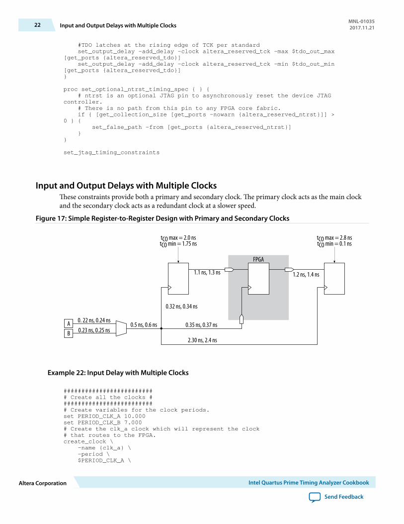
Input and Output Delays with Multiple ClocksThese constraints provide both a primary and secondary clock. The primary clock acts as the main clockand the secondary clock acts as a redundant clock at a slower speed.
Figure 17: Simple Register-to-Register Design with Primary and Secondary Clocks
FPGA
tCO max = 2.0 nstCO min = 1.75 ns
AB
tCO max = 2.8 nstCO min = 0.1 ns
1.1 ns, 1.3 ns
0.23 ns, 0.25 ns0.5 ns, 0.6 ns
0.32 ns, 0.34 ns
0.35 ns, 0.37 ns
2.30 ns, 2.4 ns
0. 22 ns, 0.24 ns
1.2 ns, 1.4 ns
Example 22: Input Delay with Multiple Clocks
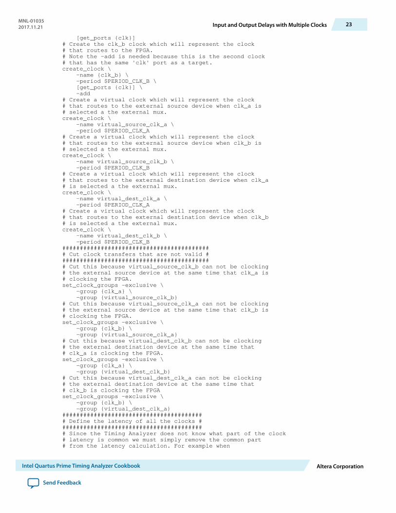
########################## Create all the clocks ########################### Create variables for the clock periods.set PERIOD_CLK_A 10.000set PERIOD_CLK_B 7.000# Create the clk_a clock which will represent the clock# that routes to the FPGA.create_clock \ -name {clk_a} \ -period \ $PERIOD_CLK_A \
22 Input and Output Delays with Multiple ClocksMNL-010352017.11.21
Altera Corporation Intel Quartus Prime Timing Analyzer Cookbook
Send Feedback
[get_ports {clk}]# Create the clk_b clock which will represent the clock# that routes to the FPGA.# Note the -add is needed because this is the second clock# that has the same 'clk' port as a target.create_clock \ -name {clk_b} \ -period $PERIOD_CLK_B \ [get_ports {clk}] \ -add# Create a virtual clock which will represent the clock# that routes to the external source device when clk_a is# selected a the external mux.create_clock \ -name virtual_source_clk_a \ -period $PERIOD_CLK_A# Create a virtual clock which will represent the clock# that routes to the external source device when clk_b is# selected a the external mux.create_clock \ -name virtual_source_clk_b \ -period $PERIOD_CLK_B# Create a virtual clock which will represent the clock# that routes to the external destination device when clk_a# is selected a the external mux.create_clock \ -name virtual_dest_clk_a \ -period $PERIOD_CLK_A# Create a virtual clock which will represent the clock# that routes to the external destination device when clk_b# is selected a the external mux.create_clock \ -name virtual_dest_clk_b \ -period $PERIOD_CLK_B########################################### Cut clock transfers that are not valid ############################################ Cut this because virtual_source_clk_b can not be clocking# the external source device at the same time that clk_a is# clocking the FPGA.set_clock_groups -exclusive \ -group {clk_a} \ -group {virtual_source_clk_b}# Cut this because virtual_source_clk_a can not be clocking# the external source device at the same time that clk_b is# clocking the FPGA.set_clock_groups -exclusive \ -group {clk_b} \ -group {virtual_source_clk_a}# Cut this because virtual_dest_clk_b can not be clocking# the external destination device at the same time that# clk_a is clocking the FPGA.set_clock_groups -exclusive \ -group {clk_a} \ -group {virtual_dest_clk_b}# Cut this because virtual_dest_clk_a can not be clocking# the external destination device at the same time that# clk_b is clocking the FPGAset_clock_groups -exclusive \ -group {clk_b} \ -group {virtual_dest_clk_a}######################################### Define the latency of all the clocks ########################################## Since the Timing Analyzer does not know what part of the clock# latency is common we must simply remove the common part# from the latency calculation. For example when
MNL-010352017.11.21 Input and Output Delays with Multiple Clocks 23
Intel Quartus Prime Timing Analyzer Cookbook Altera Corporation
Send Feedback
# calculating the latency for virtual_source_clk_a we must# ignore the 220ps,240ps route and the 500ps/600ps mux# delay if we want to remove the common clock path# pessimism.## Define fastest and slowest virtual_source_clk_a path to# the external source device.set_clock_latency -source \ -early .320 \[get_clocks virtual_source_clk_a]set_clock_latency -source \ -late .340 \ [get_clocks virtual_source_clk_a]# Define fastest and slowest virtual_source_clk_b path to# the external source device.set_clock_latency -source \ -early .320 \ [get_clocks virtual_source_clk_b]set_clock_latency -source \ -late .340 \ [get_clocks virtual_source_clk_b]# Define fastest and slowest clk_a path to the FPGA.set_clock_latency -source \ -early .350 \ [get_clocks clk_a]set_clock_latency -source \ -late .370 \ [get_clocks clk_a]# Define fastest and slowest clk_b path to the FPGA.set_clock_latency -source \ -early .350 \ [get_clocks clk_b]set_clock_latency -source \ -late .370 \ [get_clocks clk_b]# Define fastest and slowest virtual_dest_clk_a path to# the external destination device.set_clock_latency -source \ -early 2.3 \ [get_clocks virtual_dest_clk_a]set_clock_latency -source \ -late 2.4 \ [get_clocks virtual_dest_clk_a]# Define fastest and slowest virtual_dest_clk_b path to# the external destination device.set_clock_latency -source \ -early 2.3 \ [get_clocks virtual_dest_clk_b]set_clock_latency -source \ -late 2.4 \ [get_clocks virtual_dest_clk_b]###################################### Constrain the input port 'datain' ####################################### This Tco is the min/max value of the Tco for the# external module.set Tco_max 2.0set Tco_min 1.75# Td is the min/max trace delay of datain from the# external deviceset Td_min 1.1set Td_max 1.3# Calculate the input delay numbersset input_max [expr $Td_max + $Tco_max]set input_min [expr $Td_min + $Tco_min]# Create the input delay constraints when clk_a is selectedset_input_delay \
24 Input and Output Delays with Multiple ClocksMNL-010352017.11.21
Altera Corporation Intel Quartus Prime Timing Analyzer Cookbook
Send Feedback
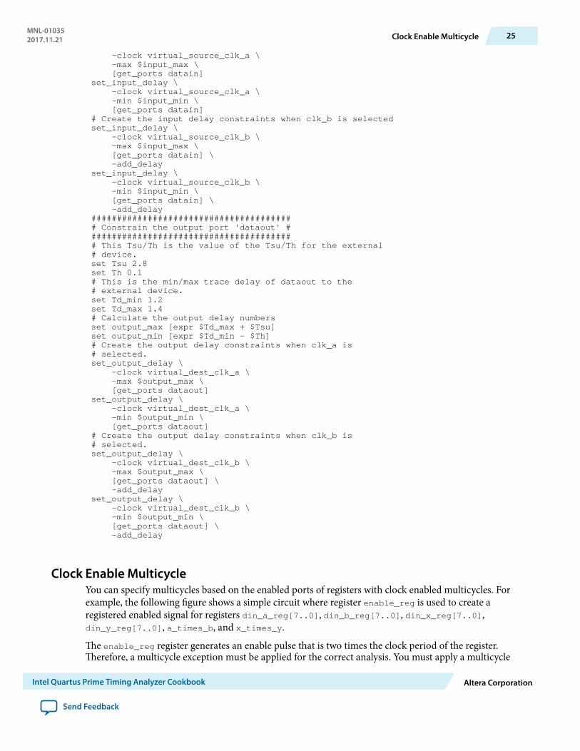
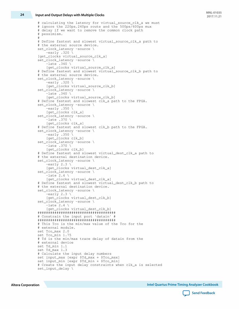
-clock virtual_source_clk_a \ -max $input_max \ [get_ports datain]set_input_delay \ -clock virtual_source_clk_a \ -min $input_min \ [get_ports datain]# Create the input delay constraints when clk_b is selectedset_input_delay \ -clock virtual_source_clk_b \ -max $input_max \ [get_ports datain] \ -add_delayset_input_delay \ -clock virtual_source_clk_b \ -min $input_min \ [get_ports datain] \ -add_delay######################################## Constrain the output port 'dataout' ######################################### This Tsu/Th is the value of the Tsu/Th for the external# device.set Tsu 2.8set Th 0.1# This is the min/max trace delay of dataout to the# external device.set Td_min 1.2set Td_max 1.4# Calculate the output delay numbersset output_max [expr $Td_max + $Tsu]set output_min [expr $Td_min - $Th]# Create the output delay constraints when clk_a is# selected.set_output_delay \ -clock virtual_dest_clk_a \ -max $output_max \ [get_ports dataout]set_output_delay \ -clock virtual_dest_clk_a \ -min $output_min \ [get_ports dataout]# Create the output delay constraints when clk_b is# selected.set_output_delay \ -clock virtual_dest_clk_b \ -max $output_max \ [get_ports dataout] \ -add_delayset_output_delay \ -clock virtual_dest_clk_b \ -min $output_min \ [get_ports dataout] \ -add_delay
Clock Enable MulticycleYou can specify multicycles based on the enabled ports of registers with clock enabled multicycles. Forexample, the following figure shows a simple circuit where register enable_reg is used to create aregistered enabled signal for registers din_a_reg[7..0], din_b_reg[7..0], din_x_reg[7..0],din_y_reg[7..0], a_times_b, and x_times_y.
The enable_reg register generates an enable pulse that is two times the clock period of the register.Therefore, a multicycle exception must be applied for the correct analysis. You must apply a multicycle
MNL-010352017.11.21 Clock Enable Multicycle 25
Intel Quartus Prime Timing Analyzer Cookbook Altera Corporation
Send Feedback
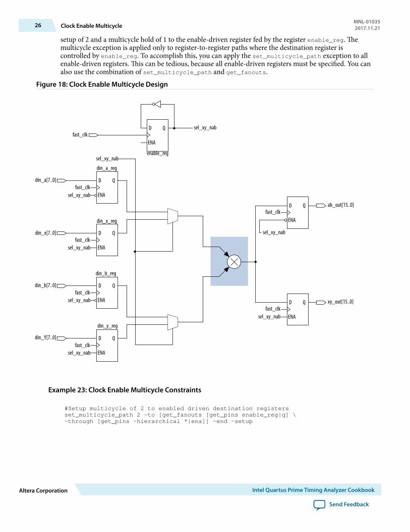
setup of 2 and a multicycle hold of 1 to the enable-driven register fed by the register enable_reg. Themulticycle exception is applied only to register-to-register paths where the destination register iscontrolled by enable_reg. To accomplish this, you can apply the set_multicycle_path exception to allenable-driven registers. This can be tedious, because all enable-driven registers must be specified. You canalso use the combination of set_multicycle_path and get_fanouts.
Figure 18: Clock Enable Multicycle Design
ENA
enable_reg
fast_clk
fast_clk
din_a[7..0]
fast_clk
fast_clk
fast_clk
din_x[7..0]
din_b[7..0]
din_Y[7..0]
D Q
ENA
D Q
ENA
sel_xy_nab
fast_clk
fast_clk
D Q
ENA
D Q
ENA
D Q
ENA
D Q
ENA
D Q
ab_out[15..0]
xy_out[15..0]
din_a_reg
din_b_reg
din_x_reg
din_y_reg
sel_xy_nab
sel_xy_nab
sel_xy_nab
sel_xy_nab
sel_xy_nab
sel_xy_nab
sel_xy_nab
Example 23: Clock Enable Multicycle Constraints
#Setup multicycle of 2 to enabled driven destination registersset_multicycle_path 2 -to [get_fanouts [get_pins enable_reg|q] \-through [get_pins -hierarchical *|ena]] -end -setup
26 Clock Enable MulticycleMNL-010352017.11.21
Altera Corporation Intel Quartus Prime Timing Analyzer Cookbook
Send Feedback
The target of the set_multicycle_path exception is limited to all fan-outs of the enable_reg registerthat feed the enable port of a register. Use the following option:
[get_fanouts [get_pins enable_reg|q] -through [get_pins -hierarchical *|ena]]
The setup and hold relationships start at the enable_reg register and end at any enable-driven register at2 and 1, respectively.
Related InformationThe Intel Quartus Prime Timing AnalyzerFor more information about multicycle exceptions refer to the Timing Analyzer Chapter in volume 3 ofthe Intel Quartus Prime Handbook.
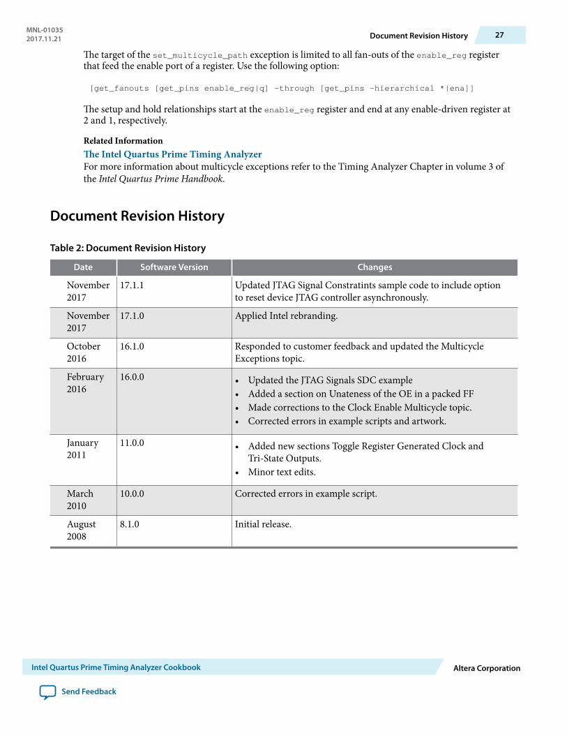
Document Revision History
Table 2: Document Revision History
Date Software Version Changes
November2017
17.1.1 Updated JTAG Signal Constratints sample code to include optionto reset device JTAG controller asynchronously.
November2017
17.1.0 Applied Intel rebranding.
October2016
16.1.0 Responded to customer feedback and updated the MulticycleExceptions topic.
February2016
16.0.0 • Updated the JTAG Signals SDC example• Added a section on Unateness of the OE in a packed FF• Made corrections to the Clock Enable Multicycle topic.• Corrected errors in example scripts and artwork.
January2011
11.0.0 • Added new sections Toggle Register Generated Clock andTri-State Outputs.
• Minor text edits.
March2010
10.0.0 Corrected errors in example script.
August2008
8.1.0 Initial release.
MNL-010352017.11.21 Document Revision History 27
Intel Quartus Prime Timing Analyzer Cookbook Altera Corporation
Send Feedback