Embed Size (px)
Citation preview
DESIGN OFHIGH ACCURACY POWERSCALABLE
MEMS SENSOR INTERFACE
by
Akram Nafee
A thesis submitted in conformity with the requirementsfor the degree of Master of Applied Science
Graduate Department of Electrical and Computer EngineeringUniversity of Toronto
© Copyright by Akram Nafee 2008
DESIGN OFHIGH ACCURACY POWER SCALABLEMEMS SENSOR INTERFACE
Akram Nafee
Master of Applied Science, 2008Graduate Department of Electrical and Computer Engineering
University of Toronto
ABSTRACT
A TECHNIQUE to improve power scaling efficiency of automotiveMEMS pressure
sensor interfaces is presented. The overall power consumption of the interface is
inversely proportional to the square of the amplitude and directly proportional to the in-
put bandwidth. Power scaling with respect to amplitude is achieved by using a novel
technique of cascading gain stages through an input gain-select mux, which scales bet-
ter than previous approaches. Power scaling with respect toinput bandwidth of the sensor
is achieved through periodic power-down of the interface. Aprototype of the interface
was fabricated in a 1.8V , 0.18µm CMOS process. Its power consumption scales between
4µW −5.33mW , while maintaining a Spurious Free Dynamic Range (SFDR) range of ap-
proximately 72− 92dB, a Total Harmonic Distortion (THD) range of 70− 90dB, and an
input referred noise of 170.0nV /√
Hz.
i

Acknowledgment
All Praise is Due to God, The Most Gracious, TheMost Merciful
T HIS work would not have been possible without the guidance, help, and support of
those who I have come to cherish as teachers, mentors, friends, and family. I would
like to thank Professor David Johns, who had guided me throughout my Masters tenure,
and has contributed significantly into shaping me to become amixed signal designer, and
a researcher. His faith in my abilities, and his expectations of excellence have driven me to
heights I would not have reached otherwise. I would also liketo thank professor Kenneth
Martin, who, although is not my supervisor, would never let an opportunity pass without
lending me his sincere feedback, and advice. I would also like to thank Johan Vanderhaegen
and Christoph Lang from BOSCH Research and Technology Center (RTC), who funded
and collaborated with us in this project. I am also immenselyindebted to the ‘PhD Group’
who I consider my mentors: Imran Ahmed, Ahmed Gharbiya, Trevor Caldwell, and Bert
Leesti. Their support and mentorship was a key factor in the success of this project. I would
also like to thank the pillars that brought me into this world, my mother and father, who
willingly sacrificed more than I could ever repay them, to make me into the man I am today.
Finally, saving the best for last, I would like to thank my dear and beloved wife, Samar,
who has brought focus into my life, and through her love and support, helped me through
the tough times of this project. I sincerely hope I am able to be as good to the people who
have been good to me, and who contributed to my growth as a person, and as an engineer.
ii
Contents
List of Tables vi
List of Figures vii
Chapter 1 Introduction 11.1 Motivation . . . . . . . . . . . . . . . . . . . . . . . . . . . . . . . . . . . 11.2 Thesis Outline . . . . . . . . . . . . . . . . . . . . . . . . . . . . . . . . . 4
Chapter 2 Background 52.1 Pressure Sensors . . . . . . . . . . . . . . . . . . . . . . . . . . . . . . . 6
2.1.1 Pressure Sensor Applications and Requirements . . . . .. . . . . . 62.1.2 Pressure Sensor Types . . . . . . . . . . . . . . . . . . . . . . . . 72.1.3 Piezoresistive Pressure Sensor . . . . . . . . . . . . . . . . . .. . 92.1.4 Gage Factor and The Piezoresistive Coefficient . . . . . .. . . . . 112.1.5 Wheatstone Bridge . . . . . . . . . . . . . . . . . . . . . . . . . . 13
2.2 Dynamic Offset and 1/F Noise Cancellation Techniques . . . . . . . . . . 142.2.1 Sources of Offset and 1/F Noise . . . . . . . . . . . . . . . . . . . 152.2.2 Auto-zeroing . . . . . . . . . . . . . . . . . . . . . . . . . . . . . 162.2.3 Chopping . . . . . . . . . . . . . . . . . . . . . . . . . . . . . . . 20
2.3 High Accuracy ADC Architectures . . . . . . . . . . . . . . . . . . . .. . 252.3.1 Flash ADC . . . . . . . . . . . . . . . . . . . . . . . . . . . . . . 252.3.2 Pipeline ADC . . . . . . . . . . . . . . . . . . . . . . . . . . . . . 252.3.3 Dual-Slope (Integrating) ADC . . . . . . . . . . . . . . . . . . . .262.3.4 ∆−Σ ADC . . . . . . . . . . . . . . . . . . . . . . . . . . . . . . 272.3.5 Incremental ADC . . . . . . . . . . . . . . . . . . . . . . . . . . . 27
Chapter 3 The Sensor Interface System 293.1 Programmable Gain Amplifier (PGA) and System Requirements . . . . . . 29
3.1.1 Incremental ADC topology . . . . . . . . . . . . . . . . . . . . . . 313.2 Variable Input and Feedback PGA . . . . . . . . . . . . . . . . . . . . .. 31
3.2.1 Variable Feedback PGA . . . . . . . . . . . . . . . . . . . . . . . 32
iii

Contents iv
3.2.2 Variable Input PGA . . . . . . . . . . . . . . . . . . . . . . . . . . 353.2.3 Variable Input and Feedback PGA . . . . . . . . . . . . . . . . . . 37
3.3 Cascade Gain PGA . . . . . . . . . . . . . . . . . . . . . . . . . . . . . . 383.3.1 Cascaded Gain Amplifier with Output Gain Select . . . . . .. . . 393.3.2 Cascaded Gain Amplifier with Input Gain Select . . . . . . .. . . 393.3.3 Switched Cap Vs Continuous Time PGA’s . . . . . . . . . . . . . .423.3.4 RC Cascaded Amplifiers . . . . . . . . . . . . . . . . . . . . . . . 47
3.4 Frequency Power Scaling: Periodic Power Down . . . . . . . . .. . . . . 48
Chapter 4 Circuit Level Implementation and Simulations 504.1 Operational Amplifiers . . . . . . . . . . . . . . . . . . . . . . . . . . . .50
4.1.1 Opamp Topology and Sizes . . . . . . . . . . . . . . . . . . . . . 514.1.2 Common Mode Feedback (CMFB) . . . . . . . . . . . . . . . . . 534.1.3 Chopper Switches . . . . . . . . . . . . . . . . . . . . . . . . . . 534.1.4 Bias Circuit Power Down . . . . . . . . . . . . . . . . . . . . . . 54
4.2 Output Buffer Stage . . . . . . . . . . . . . . . . . . . . . . . . . . . . . . 554.3 Chopping Clock Generation . . . . . . . . . . . . . . . . . . . . . . . . .584.4 Gain and Buffer Select Mux . . . . . . . . . . . . . . . . . . . . . . . . . 584.5 Design for Testability: Analog Test Mux . . . . . . . . . . . . . .. . . . . 594.6 Key Simulation Results . . . . . . . . . . . . . . . . . . . . . . . . . . . .60
Chapter 5 Experimental Results 635.1 IC Fabrication . . . . . . . . . . . . . . . . . . . . . . . . . . . . . . . . . 635.2 Test Setup . . . . . . . . . . . . . . . . . . . . . . . . . . . . . . . . . . . 64
5.2.1 System Level Representation . . . . . . . . . . . . . . . . . . . . .645.2.2 Printed Circuit Board . . . . . . . . . . . . . . . . . . . . . . . . . 655.2.3 IC Test Methodology . . . . . . . . . . . . . . . . . . . . . . . . . 66
5.3 Signal Generator Characterization . . . . . . . . . . . . . . . . .. . . . . 685.4 ADC Characterization . . . . . . . . . . . . . . . . . . . . . . . . . . . . 695.5 IC Test Results . . . . . . . . . . . . . . . . . . . . . . . . . . . . . . . . 71
5.5.1 DC Bias Points . . . . . . . . . . . . . . . . . . . . . . . . . . . . 715.5.2 Spurious Free Dynamic Range (SFDR) . . . . . . . . . . . . . . . 735.5.3 Total Harmonic Distortion (THD) . . . . . . . . . . . . . . . . . .765.5.4 Power Scaling . . . . . . . . . . . . . . . . . . . . . . . . . . . . 785.5.5 Effects of Chopping . . . . . . . . . . . . . . . . . . . . . . . . . 81
5.6 Summary . . . . . . . . . . . . . . . . . . . . . . . . . . . . . . . . . . . 83
Chapter 6 Conclusion 856.1 Future Work . . . . . . . . . . . . . . . . . . . . . . . . . . . . . . . . . . 85
Appendix A Output Noise of a Cascaded Amplifier with Input Gain Select 87

Contents v
References 89
List of Tables
2.1 Atmospheric Pressure ranges . . . . . . . . . . . . . . . . . . . . . . .. . . . 72.2 Automotive pressure sensor’s pressure and temperatureranges . . . . . . . . . 72.3 Trade-offs betweenNiCr and Polysilicon as a sensing layer (*: very good, 0:
sufficient) . . . . . . . . . . . . . . . . . . . . . . . . . . . . . . . . . . . . . 10
4.1 Opamp Transistor Sizing for the three stage cascade amplifier . . . . . . . . . 524.2 AC Simulation Parameters for the Three Amplifiers . . . . . .. . . . . . . . . 524.3 CMFB Transistor Sizing for the three stage cascade amplifier . . . . . . . . . 544.4 Input and Output Chopper Switch Sizing . . . . . . . . . . . . . . .. . . . . . 554.5 Opamp Transistor Sizing for the three stage cascade amplifier . . . . . . . . . 574.6 Simulated Power Consumption . . . . . . . . . . . . . . . . . . . . . . .. . . 62
5.1 DC Bias Points: Simulated and Measured . . . . . . . . . . . . . . .. . . . . 735.2 Simulated Vs Measured Power Consumption . . . . . . . . . . . . .. . . . . 835.3 Results Summary for Input = 40mVpp - 100mVpp . . . . . . . . . . . . . . . . 845.4 Results Summary for Input = 100mVpp - 200mVpp . . . . . . . . . . . . . . . . 845.5 Results Summary for Input = 200mVpp - 400mVpp . . . . . . . . . . . . . . . . 84
vi

List of Figures
1.1 Sensors in a modern car (Acquired from BOSCH RTC [1]) . . . .. . . . . . . 21.2 BOSCH’s MEMS sensor production volume (Acquired from BOSCH RTC [1]) 3
2.1 A typical sensor system . . . . . . . . . . . . . . . . . . . . . . . . . . . .. . 52.2 (left) A piezocapacitive sensor, and(right) a piezoelectric sensor . . . . . . . . 82.3 Measuring capacitance on piezocap sensor . . . . . . . . . . . .. . . . . . . . 82.4 Cross section of a steel-substrate piezoresistive pressure sensor . . . . . . . . . 102.5 Cross section of a Silicon piezoresistive pressure sensor . . . . . . . . . . . . . 112.6 A Wheatstone Bridge . . . . . . . . . . . . . . . . . . . . . . . . . . . . . . .132.7 (top) Top view of piezoresistive sensor,(middle) cross sectional view, and(bot-
tom) stress plot along the diaphragm length . . . . . . . . . . . . . . . . . .. 142.8 Typical Amplifier Noise spectrum . . . . . . . . . . . . . . . . . . . .. . . . 162.9 Input referred noise of a differential pair . . . . . . . . . . .. . . . . . . . . . 162.10 An auto-zeroing amplifier . . . . . . . . . . . . . . . . . . . . . . . . .. . . . 172.11 operation of auto-zeroing amplifier during(a) phaseφ1 and(b) phaseφ2 . . . . 172.12 A switch-cap amplifier using CDS . . . . . . . . . . . . . . . . . . . .. . . . 182.13 Noise spectrum of auto-zeroed switch capacitor amplifier . . . . . . . . . . . . 192.14 System diagram of the chopping principle with time and frequency domain plots 202.15 Implementation of the chopper . . . . . . . . . . . . . . . . . . . . .. . . . . 212.16 A chopper amplifier with feedback . . . . . . . . . . . . . . . . . . .. . . . . 222.17 A two-stage chopper amplifier . . . . . . . . . . . . . . . . . . . . . .. . . . 222.18 Sensor system with demodulation in the digital domain .. . . . . . . . . . . . 232.19 Chopping switching spikes . . . . . . . . . . . . . . . . . . . . . . . .. . . . 24
3.1 The Sensor Interface System of Choice . . . . . . . . . . . . . . . .. . . . . . 303.2 2nd-Order Incremental ADC Model with Input Feed-Forward . . . . .. . . . . 313.3 SQNR Vs OSR for the 2nd-Order Incremental ADC Model with Input Feed-
Forward . . . . . . . . . . . . . . . . . . . . . . . . . . . . . . . . . . . . . . 323.4 Programmable Gain Amplifier (Single ended representation) with Variable Feed-
back Impedance . . . . . . . . . . . . . . . . . . . . . . . . . . . . . . . . . . 323.5 Variable Feedback PGAs with different gain settings . . .. . . . . . . . . . . 34
vii

List of Figures viii
3.6 Variable Feedback SC PGA with different gain settings . .. . . . . . . . . . . 353.7 Programmable Gain Amplifier (Single ended representation) with Variable In-
put Impedance . . . . . . . . . . . . . . . . . . . . . . . . . . . . . . . . . . . 363.8 Variable Input PGAs with different gain settings . . . . . .. . . . . . . . . . . 363.9 Variable Input SC PGA with different gain settings . . . . .. . . . . . . . . . 373.10 Variable Input and Feedback SC PGA with different gain settings . . . . . . . . 383.11 Cascaded Gain stage with output gain select mux . . . . . . .. . . . . . . . . 393.12 Cascaded Switched Capacitor Amplifier with Input Gain Select Mux . . . . . . 403.13 Switched capacitor amplifier . . . . . . . . . . . . . . . . . . . . . .. . . . . 423.14 Noise model of Inverting R-amplifier . . . . . . . . . . . . . . . .. . . . . . . 443.15 Noise Model of active RC stage . . . . . . . . . . . . . . . . . . . . . .. . . 463.16 Cascaded active RC-Gain stage . . . . . . . . . . . . . . . . . . . . .. . . . . 473.17 Cascaded Gain stage with final active RC stage . . . . . . . . .. . . . . . . . 483.18 Power Down cycle of the interface . . . . . . . . . . . . . . . . . . .. . . . . 48
4.1 The two-stage chopper amplifier . . . . . . . . . . . . . . . . . . . . .. . . . 514.2 two-stage chopped Opamp circuit diagram . . . . . . . . . . . . .. . . . . . . 514.3 CMFB circuit . . . . . . . . . . . . . . . . . . . . . . . . . . . . . . . . . . . 544.4 Chopper switch implementation: transmission gate . . . .. . . . . . . . . . . 544.5 Opamp bias with power down switches . . . . . . . . . . . . . . . . . .. . . . 554.6 Output buffer topology . . . . . . . . . . . . . . . . . . . . . . . . . . . .. . 564.7 Buffer Opamp circuit . . . . . . . . . . . . . . . . . . . . . . . . . . . . . .. 574.8 Non-overlapping chopper clock generator . . . . . . . . . . . .. . . . . . . . 584.9 Circuit implementation of input select Mux . . . . . . . . . . .. . . . . . . . 594.10 Implementation of the analog test mux . . . . . . . . . . . . . . .. . . . . . . 604.11 THD Vs Input Amplitude with different Gain settings . . .. . . . . . . . . . . 614.12 Power Vs Input Amplitude . . . . . . . . . . . . . . . . . . . . . . . . . .. . 62
5.1 DUT Die Photo . . . . . . . . . . . . . . . . . . . . . . . . . . . . . . . . . . 645.2 System Diagram of The Test Setup . . . . . . . . . . . . . . . . . . . . .. . . 655.3 Printed Circuit Board Layout . . . . . . . . . . . . . . . . . . . . . . .. . . . 665.4 Power-Down Cycle (a)intended operation, and (b)measured . . . . . . . . . . . 675.5 Signal Generator Spectra with different output amplitudes,F = 481.605Hz . . 685.6 Signal Generator Spectra with different output amplitudes,F = 243.187Hz . . 695.7 SFDR Vs Input amplitude of the External ADC . . . . . . . . . . . .. . . . . 705.8 THD7 Vs Input amplitude of the External ADC . . . . . . . . . . . .. . . . . 705.9 ADC Characterization Spectra,Fin = 481.605Hz . . . . . . . . . . . . . . . . 715.10 SFDR Vs Input amplitude of the External ADC . . . . . . . . . . .. . . . . . 725.11 THD3 Vs Input amplitude of the External ADC . . . . . . . . . . .. . . . . . 725.12 SFDR Vs Input Amplitude with different Gain settings . .. . . . . . . . . . . 735.13 PSD plots of DUT output with different Input and Gain settings atFin = 481.6Hz 745.14 Output of DUT through a Spectrum Analyzer . . . . . . . . . . . .. . . . . . 75

List of Figures ix
5.15 SFDR with different power down modes . . . . . . . . . . . . . . . .. . . . . 765.16 PSD plots of DUT output with different Power Down modes .. . . . . . . . . 775.17 THD Vs Input Amplitude with different Gain settings . . .. . . . . . . . . . . 775.18 THD with different power down modes . . . . . . . . . . . . . . . . .. . . . 785.19 Power Vs Input Amplitude,(Fin = 481.6Hz) . . . . . . . . . . . . . . . . . . . 795.20 Power Vs Input Amplitude with different Power-Down Modes . . . . . . . . . 795.21 Frequency Power Scaling . . . . . . . . . . . . . . . . . . . . . . . . . .. . . 805.22 Frequency Power Scaling on a LOG scale . . . . . . . . . . . . . . .. . . . . 815.23 Frequency Power Scaling after removing the Ibias . . . . .. . . . . . . . . . . 815.24 Effect of Chopping with and without signal,(Fin = 481.6Hz) . . . . . . . . . . 82
A.1 Noise Model of Cascaded Gain Stage with Final Active RC Stage . . . . . . . 88

Chapter 1
Introduction
1.1 Motivation
T HE use of electronic systems in cars have increased rapidly over the last decade [1].
Some of the most important developments in the field of automotive electronics have
been in the field of automotive sensors. Currently, there areover 100 different kinds of
sensors in automobiles, which serve a variety of different functions: safety, comfort, and
drivetrain [2]. Figure 1.1 shows an example of the differentkinds of sensors in a car [3].
To put the automotive sensor market in perspective, we will mention other market sectors
here. The sensor market can be categorized as follows:
• machinery manufacturers
• processing industries
• aircraft and shipbuilding
• construction sector
• consumer electronics and applications
• automotive
• other
The automotive sensor market is worth $10.5 billion, which is 25% of the total sensor
market, making it the largest of all the other segments. In terms of projected growth, the
overall sensor market is expected to grow by 4-5% by 2010, andthe expected growth for
the automotive sensor market ranges from 5.1% to 7.5%. As such there is huge driving
force for automotive electronics, which is strongly coupled to the market drive for sensors.
1

1.1. Motivation 2
Figure 1.1: Sensors in a modern car (Acquired from BOSCH RTC [1])

1.1. Motivation 3
Because cost pressure on all automotive components are high, low-cost, high-volume
processes are a pre-requisite for automotive electronics,including sensors. Because each
sensor needs to be specifically designed for a particular function in the vehicle, generally
the electronics needed to interface with the sensor were custom designed as well, in terms
of accuracy, and power. This has led to a new drive to build power-scalable electronics,
which allows one design to be used in a multitude of applications, and be optimal for each.
This work focuses on building a novel power scalable sensor interface, whose power
scales with both frequency and input signal amplitude. The interface is designed to be
implemented for different types of sensors, and hence a widerange of sensor output am-
plitudes (40mVpp - 400mVpp) and frequencies (0.5Hz - 0.5kHz) [4]. In sensor applications,
the front-end circuitry consumes most of the power, and hence is the bottleneck for low
power applications. By making the interface power scalable, the entire system becomes
power efficient. This work is part of a larger integrated system of advanced MEMS pres-
sure sensor for automotive electronics, as well as low powerconsumer applications, such
as altimeters [1]. This project was proposed by BOSCH Electronics as part of an effort
to design an ultra-low power 14 bit Oversampling Analog to Digital Converter (ADC) for
sensor applications. BOSCH is the largest MEMS producer in the world, especially in the
automotive sector. Figure 1.2 shows the volume of automotive MEMS sensors produced by
BOSCH by 2003 in Millions per annum (Mio/a). This work has potential to increase their
BOSCH - MEMS Manufacturing Volume
0
20
40
60
80
100
120
Vo
lum
e
(Un
its i
n M
io/a
)
2000 2001 2002 2003 2004 2005
Year Turnover MEMS products 2003:
> 400 Mio EUR
Figure 1.2: BOSCH’s MEMS sensor production volume (Acquired from BOSCH RTC[1])

1.2. Thesis Outline 4
profit margins by reducing design time of making customized electronics for each sensor
application. Moreover, because of economies of scale, the design can be produced in larger
quantities, which reduces the cost per unit.
1.2 Thesis Outline
In this dissertation, the development of a 14 bit, power scalable PGA (Programmable Gain
Amplifier) as a sensor interface is discussed. In chapter two, we discuss the design of
pressure sensors in detail, design considerations in sensor applications, such as 1/ f noise
cancelation techniques, as well as high accuracy ADC architectures compatible with power-
scalability. The third chapter discusses the system designmethodology for the power scal-
able PGA, by examining and comparing alternative architectures. Power scalability tech-
niques are also described from a system level perspective. The fourth chapter describes
the circuit implementation of the power-scalable PGA, which includes the design of the
chopper amplifier, and the Power Resettable OPAMP. Key simulation results, and design
limitations are also described in this section. Chapter 5 inthis dissertation describes the
measured results, and in chapter 6 we provide key conclusions from this project, and briefly
describe potential future research topics.

Chapter 2
Background
T HE nature of sensors is that they convert one type of energy into another that can
be measured and used in different applications. As such, both the input energy, and
the output signal of the sensor are analog signals. In the case of the pressure senor, the
sensing element converts mechanical energy, into an electric signal. Since most high accu-
racy signal processing in the modern age is done in the digital domain, the sensor output
signal needs to be converted to a digital signal by an Analog to Digital Convertor (ADC).
Depending on the application, the signal may need to be amplified or buffered before it gets
to the ADC, in order to reduce the ADC area, power or complexity requirements. Figure
2.1 shows a top level representation of the sensor system.
In this chapter, we will discuss, in detail, the background material needed to design
Sensor Amplifier/Buffer
High AccuracyADC
N
ADCG
Mechanicalpressure
Analog Digital
Figure 2.1: A typical sensor system
5
2.1. Pressure Sensors 6
a high accuracy, power scalable PGA as a sensor interface. Insection 2.1, we will first
discuss the design and workings of the pressure sensor used in automotive and consumer
electronics. In section 2.2, we will discuss some of the major design considerations in
sensor applications, such as offset and 1/ f noise cancelation techniques. Finally, in section
2.3, we will discuss the different types of ADC’s that can potentially be used in sensor
applications, and some tradeoffs between topologies when designing high accuracy power
scalable systems.
2.1 Pressure Sensors
2.1.1 Pressure Sensor Applications and Requirements
As mentioned in the introduction, this work is part of a larger system of integrated pressure
sensors for, primarily, automotive sensors, and for consumer electronics. In terms of the
consumer electronics market, the primary application willbe in altimeters. In automobiles,
the pressure sensor is used in many places, some of which are:
• turbocharger pressure
• suspension
• oil pressure
• climate control
• fuel-tank pressure
• tire pressure
• brake-fluid pressure
• gasoline vapor pressure
• gasoline/diesel direct inject pressure
• Locomotive fuel inject pressure
Each of these applications have different requirements in terms of the required pressure
range that needs to be measured, the accuracy of measurement, and the temperature range
[2].
For altimeters, the requirements are to measure atmospheric levels at different heights
relative to sea level, and over a narrow temperature range. Table 2.1 shows the atmospheric
pressure, in Pascals, over the seven different atmosphericlevels.
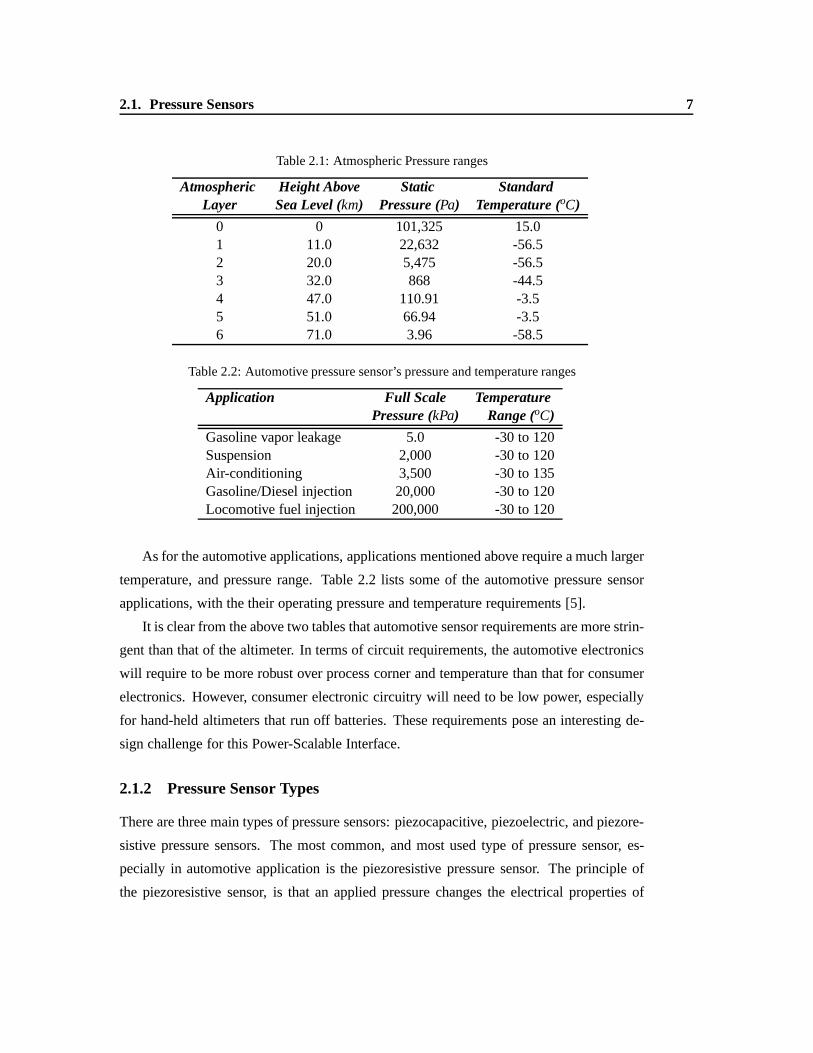
2.1. Pressure Sensors 7
Table 2.1: Atmospheric Pressure ranges
Atmospheric Height Above Static StandardLayer Sea Level (km) Pressure (Pa) Temperature (oC)
0 0 101,325 15.01 11.0 22,632 -56.52 20.0 5,475 -56.53 32.0 868 -44.54 47.0 110.91 -3.55 51.0 66.94 -3.56 71.0 3.96 -58.5
Table 2.2: Automotive pressure sensor’s pressure and temperature ranges
Application Full Scale TemperaturePressure (kPa) Range (oC)
Gasoline vapor leakage 5.0 -30 to 120Suspension 2,000 -30 to 120Air-conditioning 3,500 -30 to 135Gasoline/Diesel injection 20,000 -30 to 120Locomotive fuel injection 200,000 -30 to 120
As for the automotive applications, applications mentioned above require a much larger
temperature, and pressure range. Table 2.2 lists some of theautomotive pressure sensor
applications, with the their operating pressure and temperature requirements [5].
It is clear from the above two tables that automotive sensor requirements are more strin-
gent than that of the altimeter. In terms of circuit requirements, the automotive electronics
will require to be more robust over process corner and temperature than that for consumer
electronics. However, consumer electronic circuitry willneed to be low power, especially
for hand-held altimeters that run off batteries. These requirements pose an interesting de-
sign challenge for this Power-Scalable Interface.
2.1.2 Pressure Sensor Types
There are three main types of pressure sensors: piezocapacitive, piezoelectric, and piezore-
sistive pressure sensors. The most common, and most used type of pressure sensor, es-
pecially in automotive application is the piezoresistive pressure sensor. The principle of
the piezoresistive sensor, is that an applied pressure changes the electrical properties of

2.1. Pressure Sensors 8
diffused resistors (called piezoresistors, or gages) [5].The piezoresistive sensors will be
explained in greater detail in the next section.
Fixed Electrode
MoveableElectrode
Substrate
V
Piezoelectricmaterial
Figure 2.2:(left) A piezocapacitive sensor, and(right) a piezoelectric sensor
The piezocapactive sensor is shown in Figure 2.2. The two electrodes form a capac-
itance, which changes when a pressure is applied. When the diaphragm is distorted due
to pressure, the width of the gap between the electrodes changes, which translates into a
change of capacitance. That capacitance change can be measured by using an Opamp with
a fixed feedback capacitor, as shown in Figure 2.3.
The principle of the piezoelectric sensor is also shown in figure 2.2. The applied pres-
sure to an appropriate material distorts its shape, and generates a voltage which can be
measured.
+
-
Cfixed
Csensor
Figure 2.3: Measuring capacitance on piezocap sensor

2.1. Pressure Sensors 9
2.1.3 Piezoresistive Pressure Sensor
As mentioned in the previous section, piezoresistive pressure sensors are the most com-
monly used types in automotive and consumer application, because of their high accuracy,
and potentially low cost of manufacture. There are two typesof piezoresistive pressure
sensors: The silicon piezoresistive sensor, and the steel-substrate piezoresistive sensor. The
silicon pressure sensor is used for low-medium pressure measurements, whereas the steel-
substrate sensor is used in high-pressure applications. Figures 2.4 and 2.5 show the cross
section of the steel-substrate, and silicon pressure sensors, respectively.
In terms of fabrication, the functional layers of any piezoresistive sensor are [5]:
• Substrate layer: The substrate is the transducer that detects strain, and is an important
layer of the pressure sensor. Properties such as high resistance to corrosive material
and low brittleness are important in enhancing the performance of the sensor.
• Isolation layer: This layer is to be used as insulation between the piezoresistors and
the substrate. It also serves the function of transmitting the elastic deformations from
the substrate to the piezoresistors. The material has to exhibit high thermal stability,
and resist cracking.
• Sensing layer: This refers to the piezoresistors, or gage resistors. Their function
is to transform mechanical stress into electrical energy. They should exhibit low
temperature dependance on their electrical properties, high resistivity, and a strong
correlation between the applied strain and resistance. More details of their properties
as sensing layers are described in the next section.
• Passivation Layer: This layer protects the gage resistorsfrom environmental expo-
sure. the passivation layer should have high resistance to moisture and ion penetra-
tion, high insulation properties, and high thermal stability.
Steel-Substrate Piezoresistive Sensor
Figure 2.4 shows a cross section of the functional layers of asteel-substrate piezoresistive
sensor. Stainless steel is used as a substrate material because of its high strength, its tem-
perature stability, and its high corrosion stability. Because of these substrate properties, the
steel pressure sensors are used for high pressure applications. The isolation layer is often
made fromSiO2 or Al2O3, because of their good dielectric properties.SiO2 is preferred

2.1. Pressure Sensors 10
Diaphragm
Piezoresistor(Sensing Layer)
Silicon Nitride,Si
3N
4
(Passivation Layer)
SiO2
(Isolation Layer)
Steel(Substrate
Layer)
Gold (Au)Contact
Figure 2.4: Cross section of a steel-substrate piezoresistive pressure sensor
because its insulating properties are superior to that ofAl2O3. The sensing layer is often
chosen to be p-doped polysilicon, because it has a high correlation (sensitivity) between
stress and resistance. Moreover, because of its high resistivity, it can be fabricated into a
small size.NiCr can also be used as a sensing layer for applications where lower tempera-
ture dependance, and high thermal stability is needed. The drawback ofNiCr is that it has a
much lower correlation between stress and resistance than polysilicon. Table 2.3 shows the
trade-offs betweenNiCr and polysilicon, hence, the choice of sensing layer is dependant
upon the target application.
The passivation layer is usually made out ofSi3N4, because of its superior resistance to
humidity, and high adhesion. Finally, the metal contacts onthe resistors are usually made
out of gold, because it is most stable against corrosion [6].
Table 2.3: Trade-offs betweenNiCr and Polysilicon as a sensing layer (*: very good, 0:sufficient)
Criteria NiCr Polysilicon
Gage Factor 0 *Temperature dependance * 0Resistivity 0 *Stability * 0Reproducibility * 0

2.1. Pressure Sensors 11
Silicon Piezoresistive Sensor
Silicon based sensors have become increasingly popular over the last decade, because of
their low cost, potential for high production volume, and integration with silicon micro-
electronics. The silicon piezoresistive pressure sensor is no exception. Figure 2.5 shows
a cross sectional view of a silicon piezoresistive sensor [7]. The diaphragm, which bends
under stress and converts pressure into strain on the resistors, is etched out of the silicon
substrate. The isolation layer is made out of Epipoly, a special type of polysilicon used for
sensor applications. Details of epipoly fabrication is described in [6]. The advantage of
epipoly as an isolation layer is that it is very stable over process parameters. The piezore-
sistors are made out of p-doped polysilicon, and the passivation layer is made out ofSiO2.
When the sensor is packaged, difference in thermal expansion properties between the sen-
sor and the package can affect the sensor characteristics. The glass base is used to lessen
that effect.
Glass Base
Diaphragm
Piezoresistor(Sensing Layer)
SiO2
(Passivation Layer)Epipoly(Isolation Layer)
P+ Silicon(substrate
Layer)
Figure 2.5: Cross section of a Silicon piezoresistive pressure sensor
2.1.4 Gage Factor and The Piezoresistive Coefficient
The Gage Factor is an important parameter which helps characterize the gage resistors. It
describes the sensitivity of the resistors to the mechanical strain applied. The relationship
between the fractional change of resistance (∆R/R) , and the mechanical strain (σ ) is given

2.1. Pressure Sensors 12
by:∆RR
= KGF ·σ (2.1)
WhereKGF is the gage factor [6]. To illustrate the relationship between the gage factor and
physical contributions, we start with the expression of defining the resistanceR as:
R = ρlA
(2.2)
Whereρ is the resistivity,l is the length of the resistor, andA is the cross sectional area.
When a mechanical strain is applied, the fractional change in resistance can be expressed
to a first order approximation by:
∆RR
=∆ρρ
+∆ll−
∆AA
(2.3)
Given that:∆ll
= σ (2.4)
and:∆AA
= −2v∆ll
(2.5)
Wherev is the Poisson ratio, the relative resistance variation is given by:
∆RR
=
(
1+2v+∆ρ
ρ ·σ
)
·σ (2.6)
Which shows how the relative resistance change due to physical contributions. By equating
2.1 and 2.6, we get:
KGF = 1+2v+∆ρ
ρ ·σ(2.7)
The first two terms of this equation represent the geometrical contributions to the gage
factor, and the last term represents the change in resistivity [6]. The property by which a
material changes its resistivity due to mechanical strain is called the piezoresistive effect
[8]. The last term in this equation is called the piezoresistive coefficient, and is represented
as:
π44 =∆ρ
ρ ·σ(2.8)

2.1. Pressure Sensors 13
For silicon based gage resistors, the geometrical contribution of the gage factor is negligi-
ble, and the piezoresistive coefficient term (π44) dominates. The coefficient is also depen-
dant on the doping qualities of the semiconductor material.
2.1.5 Wheatstone Bridge
In order to detect the changes in resistance of the gage resistors, four piezoresistors are
arranged in a wheatstone bridge structure, as shown in Figure 2.6. Although currently used
for pressure sensor applications, the wheatstone bridge configuration (originally called a
“differential resistance measurer”) was invented by Samuel Hunter Christie in 1833, al-
though it was named after Charles Wheatstone, who elaborated more on the concept in
1843 [9]. The output resistance of wheatstone bridge automotive pressure sensors are typ-
R1 R2
R3 R4
Vout
VDD
Figure 2.6: A Wheatstone Bridge
ically on the order of kilo ohms. To maximize the output voltage the resistors have to ex-
perience changes in resistance that differ in sign. Refer toFigure 2.7, which shows the top
view of the gage resistor arrangement on the diaphragm, as well as the stress plot along the
diaphragm. From this stress plot, we see that the resistors in the middle of the diaphragm
experience negative stress, whereas those on the edges of the diaphragm experience pos-
itive stress [5]. Since the resistance of the gage resistorsis directly proportional to the
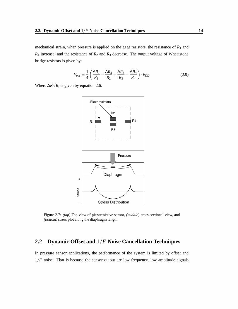
2.2. Dynamic Offset and1/F Noise Cancellation Techniques 14
mechanical strain, when pressure is applied on the gage resistors, the resistance ofR1 and
R4 increase, and the resistance ofR2 andR3 decrease. The output voltage of Wheatstone
bridge resistors is given by:
Vout =14
(
∆R1
R1−
∆R2
R2+
∆R3
R3−
∆R4
R4
)
·VDD (2.9)
Where∆Ri/Ri is given by equation 2.6.
Str
ess
+
- Stress Distribution
Pressure
Piezoresistors
Diaphragm
R1 R4
R3
R2
Figure 2.7:(top) Top view of piezoresistive sensor,(middle) cross sectional view, and(bottom) stress plot along the diaphragm length
2.2 Dynamic Offset and1/F Noise Cancellation Techniques
In pressure sensor applications, the performance of the system is limited by offset and
1/F noise. That is because the sensor output are low frequency, low amplitude signals
2.2. Dynamic Offset and1/F Noise Cancellation Techniques 15
(40mVpp − 400mVpp,0.5Hz − 0.5kHz), hence any low frequency noise or phenomenon
above the thermal noise floor need to be eliminated or mitigated. In this section we discuss
the sources of offset and 1/F noise, and the two most common methods of canceling them:
auto-zeroing, and chopping.
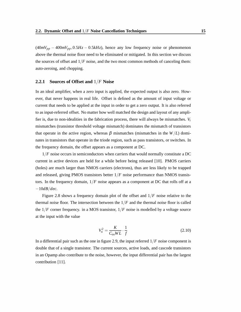
2.2.1 Sources of Offset and1/F Noise
In an ideal amplifier, when a zero input is applied, the expected output is also zero. How-
ever, that never happens in real life. Offset is defined as theamount of input voltage or
current that needs to be applied at the input in order to get a zero output. It is also referred
to as input-referred offset. No matter how well matched the design and layout of any ampli-
fier is, due to non-idealities in the fabrication process, there will always be mismatches.Vt
mismatches (transistor threshold voltage mismatch) dominates the mismatch of transistors
that operate in the active region, whereasβ mismatches (mismatches in theW/L) domi-
nates in transistors that operate in the triode region, suchas pass transistors, or switches. In
the frequency domain, the offset appears as a component at DC.
1/F noise occurs in semiconductors when carriers that would normally constitute a DC
current in active devices are held for a while before being released [10]. PMOS carriers
(holes) are much larger than NMOS carriers (electrons), thus are less likely to be trapped
and released, giving PMOS transistors better 1/F noise performance than NMOS transis-
tors. In the frequency domain, 1/F noise appears as a component at DC that rolls off at a
−10dB/dec.
Figure 2.8 shows a frequency domain plot of the offset and 1/F noise relative to the
thermal noise floor. The intersection between the 1/F and the thermal noise floor is called
the 1/F corner frequency. in a MOS transistor, 1/F noise is modelled by a voltage source
at the input with the value
V 2n =
KCoxW L
·1f
(2.10)
In a differential pair such as the one in figure 2.9, the input referred 1/F noise component is
double that of a single transistor. The current sources, active loads, and cascode transistors
in an Opamp also contribute to the noise, however, the input differential pair has the largest
contribution [11].

2.2. Dynamic Offset and1/F Noise Cancellation Techniques 16
ThermalNoise Floor
1/Fnoise
1/F CornerFrequency
Log(Frequency)
10 dB/dec
dB Offset
Figure 2.8: Typical Amplifier Noise spectrum
*
2 x Vn2
,in
Itail
Figure 2.9: Input referred noise of a differential pair
2.2.2 Auto-zeroing
Operating Principle
Auto-zeroing is a switch capacitor method of cancelling offset. Its basic principle is that
it applies a zero input to the amplifier, and measures its offset. Then, when the signal is
amplified, subtracts the measured offset from the signal [12]. Figure 2.10 shows an example
of a switch capacitor amplifier that utilizes auto-zeroing.
Clocksφ1 andφ2 are non-overlapping phases. Figure 2.11 shows the operating phases
of the above amplifier.
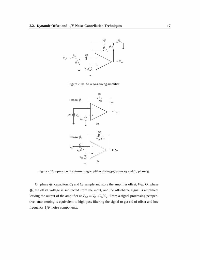
2.2. Dynamic Offset and1/F Noise Cancellation Techniques 17
-
+
C1
C2
Vin
Vout
VOS
+
-
2
21
1
1
Figure 2.10: An auto-zeroing amplifier
-
+C1
C2
Vout
VOS
+
-
VC1
VC2
+
-
+ -
-
+
C1
C2
Vout
VOS
+
-
VC1
(n-1)+-
+ -V
C2(n-1)
Vin
(a)
(b)
Phase
Phase2
1
Figure 2.11: operation of auto-zeroing amplifier during(a) phaseφ1 and(b) phaseφ2
On phaseφ1, capacitorsC1 andC2 sample and store the amplifier offset,VOS. On phase
φ2, the offset voltage is subtracted from the input, and the offset-free signal is amplified,
leaving the output of the amplifier atVout = Vin ·C1/C2. From a signal processing perspec-
tive, auto-zeroing is equivalent to high-pass filtering thesignal to get rid of offset and low
frequency 1/F noise components.

2.2. Dynamic Offset and1/F Noise Cancellation Techniques 18
Correlated Double Sampling (CDS)
Correlated Double Sampling (CDS) is another switched capacitor technique to eliminate
offset and 1/F noise. Instead of sampling the offset and then cancelling itfrom the signal,
CDS works by sampling the signal twice, and then performing alinear combination of the
two samples to eliminate the offset. Figure 2.12 shows an example of a switched capacitor
-
+
C1
C1' C2'
C2
Vin
Vout
VOS
+
-
1
1
11
1
2
2
2
2
2
Figure 2.12: A switch-cap amplifier using CDS
gain amplifier that utilizes CDS. On phaseφ2, the input is sampled on capacitorC1′, and on
phaseφ1, the input is sampled onC1, and the difference of the two input signals is amplified
by C2 andC2′ and appears at the output. The output of the CDS amplifier on phaseφ2 is
Vout = (Vin2 −Vin1)C1/C2, whereVin1 andVin2 are the input voltage at the end of phaseφ1
andφ2 respectively. Because the inputs are sampled with the offset in both phases, when
the difference is taken, the effect of the offset is not seen at the output.
CDS amplifiers are useful in applications where only the timedifference of two signals
are needed, such as image sensors. We will not go into detailsof the CDS technique, since
it is not as applicable for pressure sensors.
Design Considerations
There are some design considerations that have to be kept in mind when designing auto-
zeroing switched capacitor amplifiers. One of them is chargeinjection, which is a common
2.2. Dynamic Offset and1/F Noise Cancellation Techniques 19
problem for any switched capacitor circuit, and can be a source of distortion. Charge
injection occurs during the falling edge of a clock, and is given byQch = WLCox(VGS −Vt),
andVch = Qch/Cin. Switches must be made small, and input capacitors made large in order
to minimize their effect. However, that may cause settling issues due to a large switch on-
resistance (rON), and a largeCin. For optimal noise and power performance, the capacitance
C is sized according toKT/C noise calculations. The switch is then sized to optimize the
time constantrONCin, and the charge injection, based on simulation. There are other circuit
techniques that can minimize their effects, which can be referred to in [10].
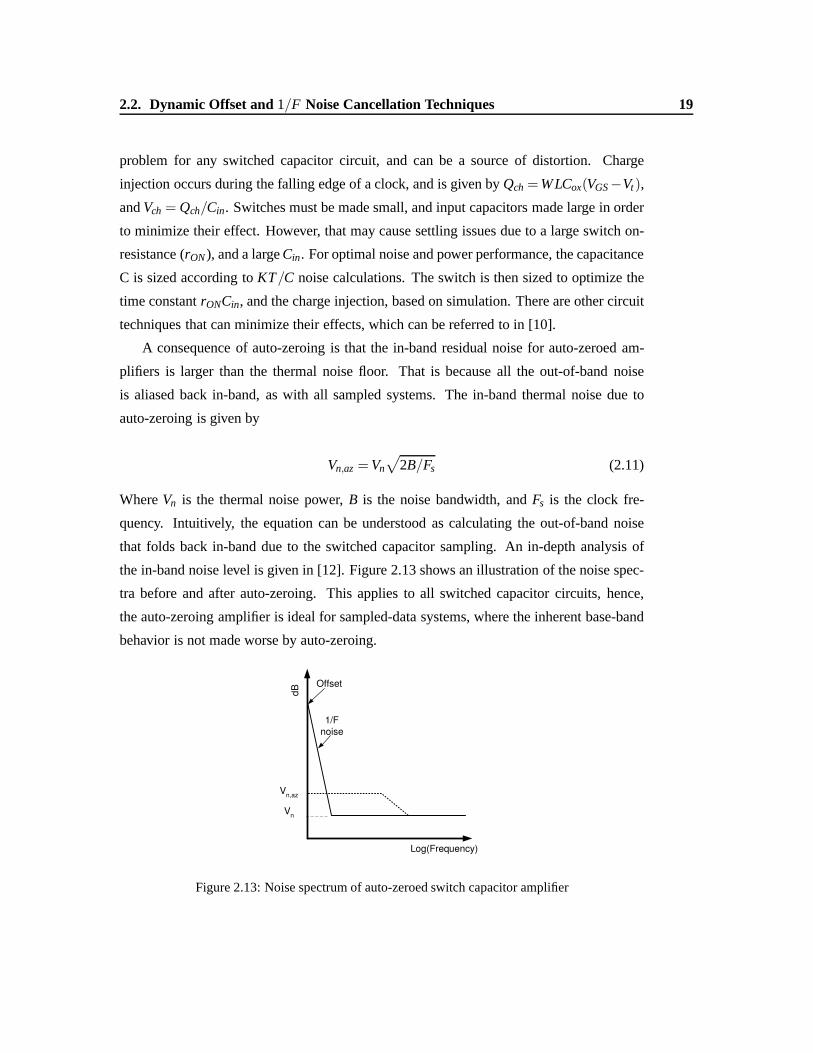
A consequence of auto-zeroing is that the in-band residual noise for auto-zeroed am-
plifiers is larger than the thermal noise floor. That is because all the out-of-band noise
is aliased back in-band, as with all sampled systems. The in-band thermal noise due to
auto-zeroing is given by
Vn,az = Vn
√
2B/Fs (2.11)
WhereVn is the thermal noise power,B is the noise bandwidth, andFs is the clock fre-
quency. Intuitively, the equation can be understood as calculating the out-of-band noise
that folds back in-band due to the switched capacitor sampling. An in-depth analysis of
the in-band noise level is given in [12]. Figure 2.13 shows anillustration of the noise spec-
tra before and after auto-zeroing. This applies to all switched capacitor circuits, hence,
the auto-zeroing amplifier is ideal for sampled-data systems, where the inherent base-band
behavior is not made worse by auto-zeroing.
Vn,az
1/Fnoise
Log(Frequency)
dB Offset
Vn
Figure 2.13: Noise spectrum of auto-zeroed switch capacitor amplifier
2.2. Dynamic Offset and1/F Noise Cancellation Techniques 20
2.2.3 Chopping
Operating Principle
0
signal
offset
Modulated
signal
Modulated
offset
Filtered
offset
Demodulated
signal signal
V1 V
2V
3V
inV
4V
out
f/fch
f/fch
f/fch
f/fch
f/fch
f/fch
signal
Modulated
signal Vos
+Vn
Modulated
Vos
+Vn
LPF
signalFrequencyDomain
TimeDomain
+ G LPF
Vos
+Vn
Vin
Vout
V1
V2
V3
V4
ch ch
Figure 2.14: System diagram of the chopping principle with time and frequency domainplots
Chopping is a continuous-time technique that uses modulation to get rid of offset and
1/F noise, as shown in figure 2.14. Using this technique, the input signal is square-wave
modulated to a higher frequency,fch before is reaches the amplifier-with-offset. Both the
signal and offset are amplified, after which the signal is demodulated back to baseband,
whereas the offset and 1/ f noise are modulated tofch. A low pass filter following the
output chopper filters out the modulated offset and 1/F noise [12].
The choppers can be easily implemented in CMOS technology using a four switches
in a polarity reversing topology, as in figure 2.15. A condition for the chopping technique
to completely eliminate the 1/F noise, is that the chopping frequency,fch, must be greater
than the 1/F corner frequency (Fc).
The advantages of chopping over auto-zeroing is that the in-band noise is equal to the
thermal noise level in chopping, whereas it is always higherin auto-zeroing. Both methods

2.2. Dynamic Offset and1/F Noise Cancellation Techniques 21
to
toV
in
Figure 2.15: Implementation of the chopper
suffer from the problem of switch sizing that can handle the necessary signal swing, and at
the same time minimize the charge injection. The disadvantage of the chopping technique
is that chopping reduces the effective gain of the amplifier,and hence increases the gain
errors [13]. The amplifier bandwidth (BW ) must be designed much larger than the chopping
frequency to reduce the gain errors. The effective gain of the chopper amplifier is given by:
Ae f f = A
(
1−4τTch
)
(2.12)
Whereτ = 1/(2π ·BW ), A is the open loop gain of the amplifier before chopping, andTch is
the chopping period [13]. If the amplifierBW is designed 6 times the chopping frequency,
then the effective gain,Ae f f , is approximately 10% lower than the open loop gain,A, of
the non-chopped amplifier. This happens because the glitches that occur due to chopping
reduces the output signal’s amplitude, and hence reduces the DC gain. How fast the opamp
can recover from the glitches will affect how much the amplitude changes, and hence affect
the effective gain.
One way to get around this problem is to perform the chopping operation within the
feedback of the amplifier. Figure 2.16 shows an example of an amplifier in feedback, where
the chopping is done within the feedback resistors. In this case, the overall amplifier gain
is less sensitive to the open loop gain of the Opamp, and hencereducing gain errors [13].
Moreover, the input choppers only see the virtual ground of the amplifier, which has a
signal amplitude ofVout/A. Since this signal is much smaller than the input signal, the
input chopper switches can be made much smaller than in the previous case where the

2.2. Dynamic Offset and1/F Noise Cancellation Techniques 22
A+
-
-
+Vin
Vout
Ri
Ri
Rf
Rf
ch ch
+-
VOS
Figure 2.16: A chopper amplifier with feedback
input choppers had to tolerate the entire input signal swing. This significantly reduces the
charge injection errors due to the input switches. The output switches still have to be made
large in order to tolerate the full output signal swing, however, their effect is reduced when
referred to the input, and hence do not significantly affect the performance. In the case
where a two stage Opamp is used, a common technique is to include the demodulation
chopper at the output of the first stage [14]. An example of that is shown in figure 2.17.
A1 A2+
-
+
-
-
+
-
+V
inV
out
Cc
Cc
Ri
Ri
Rf
Rf
chch
+-
VOS1
+-
VOS2
Figure 2.17: A two-stage chopper amplifier
Once again, the switch sizes of the second stage can be reduced, since the signal swing
2.2. Dynamic Offset and1/F Noise Cancellation Techniques 23
at the input of the second stage isVout/A2. Moreover, this method is more power efficient
than chopping across the entire two stages, since it is takesless power to make the band-
width of the first amplifier much larger thanfch, than it is to make the two-stage amplifier
bandwidth as large. In other words, this method allows chopping at higher frequencies if
necessary for the same power consumption [15]. Furthermore, due to the compensation
capacitor, the second stage acts as a low-pass filter to get rid of the chopping artifacts,
and hence greatly reduces the requirements of the external low-pass filter if required. The
disadvantage of this method, is that the offset and 1/F noise of the second stage is not
canceled, henceA1 has to be made large in order to reduce its effects when referred to the
input.
Chopping in the Digital Domain
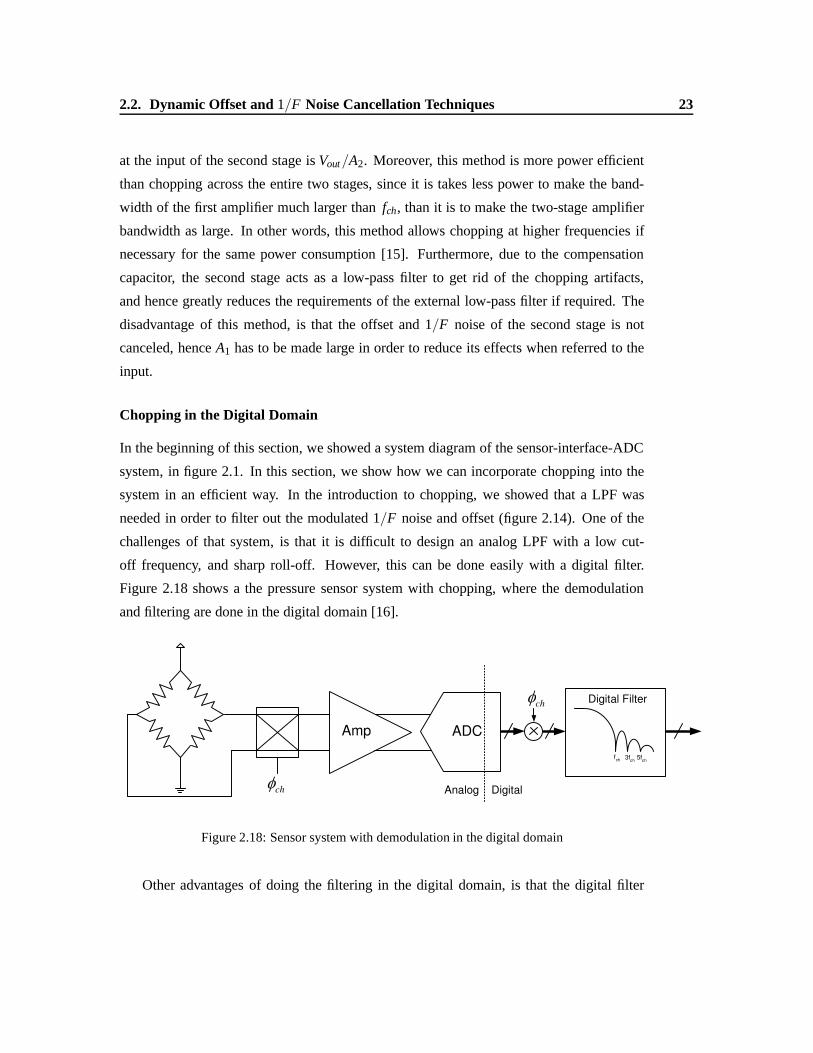
In the beginning of this section, we showed a system diagram of the sensor-interface-ADC
system, in figure 2.1. In this section, we show how we can incorporate chopping into the
system in an efficient way. In the introduction to chopping, we showed that a LPF was
needed in order to filter out the modulated 1/F noise and offset (figure 2.14). One of the
challenges of that system, is that it is difficult to design ananalog LPF with a low cut-
off frequency, and sharp roll-off. However, this can be doneeasily with a digital filter.
Figure 2.18 shows a the pressure sensor system with chopping, where the demodulation
and filtering are done in the digital domain [16].
Amp ADC
Digital Filter
fch 3f
ch5f
ch
Analog Digitalch
ch
Figure 2.18: Sensor system with demodulation in the digitaldomain
Other advantages of doing the filtering in the digital domain, is that the digital filter
2.2. Dynamic Offset and1/F Noise Cancellation Techniques 24
can be implemented with much less power consumption than an analog filter. Moreover,
the filter can be designed with notches at odd harmonics offch, which will completely
eliminate the chopping artifacts. Moreover, if an oversampling converter is used as the
ADC, then the digital filter and the decimation filter can be integrated, so there is no extra
power consumption due to filtering. Demodulating in the digital domain eliminates the
need for big switches in the signal path which degrades the signal quality due to distortion
from charge injection.
Design Considerations
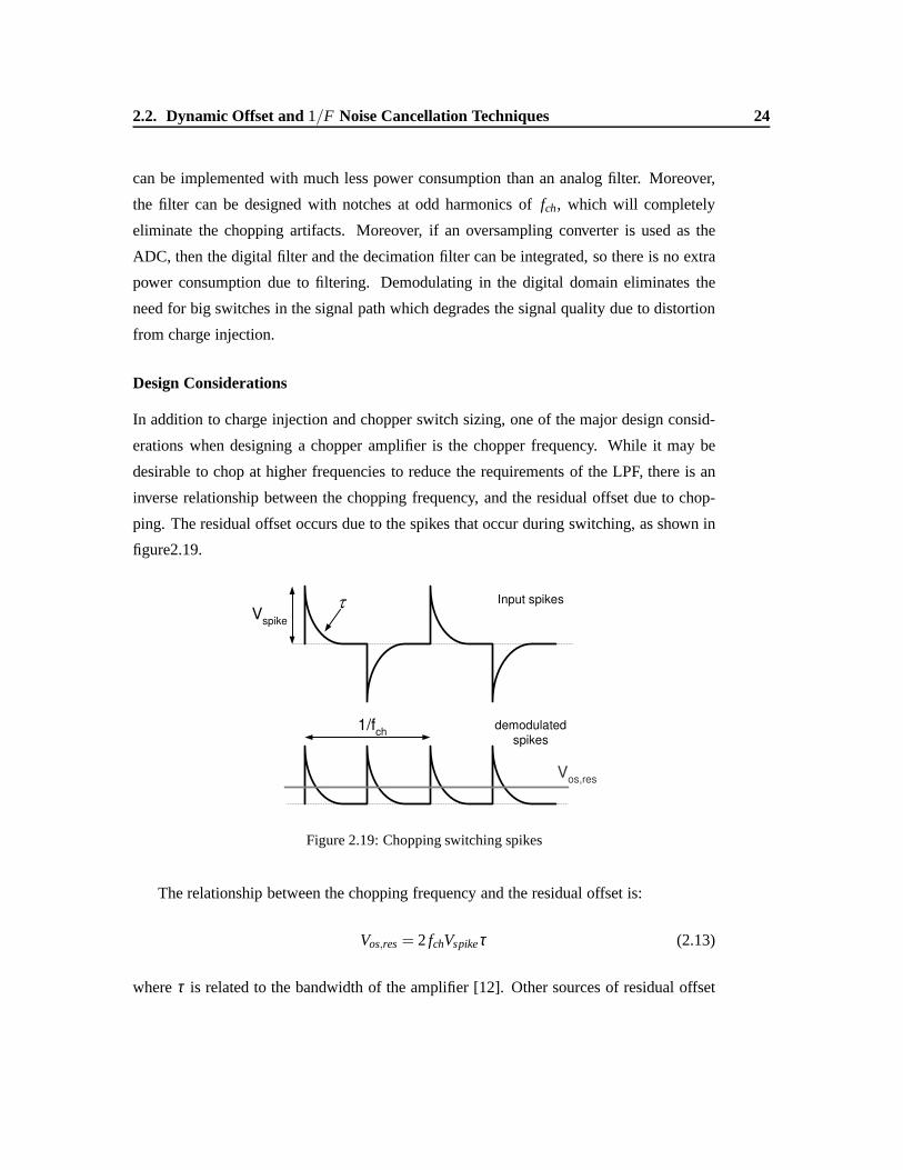
In addition to charge injection and chopper switch sizing, one of the major design consid-
erations when designing a chopper amplifier is the chopper frequency. While it may be
desirable to chop at higher frequencies to reduce the requirements of the LPF, there is an
inverse relationship between the chopping frequency, and the residual offset due to chop-
ping. The residual offset occurs due to the spikes that occurduring switching, as shown in
figure2.19.
Vspike
1/fch
Vos,res
Input spikes
demodulated
spikes
Figure 2.19: Chopping switching spikes
The relationship between the chopping frequency and the residual offset is:
Vos,res = 2 fchVspikeτ (2.13)
whereτ is related to the bandwidth of the amplifier [12]. Other sources of residual offset
2.3. High Accuracy ADC Architectures 25
is non-symmetrical layout. The choppers must be laid-out assymmetrically as possible to
ensure that the chopped signals see the same impedance, and clock coupling.
In conclusion, chopping is the dynamic offset cancellationtechnique of choice in con-
tinuous time, low bandwidth applications. There are several other amplifier topologies that
utilize chopping that can be referred to in [17] [18] [19] [20] [21]. The above topologies are
meant to introduce the concept of chopping as an offset cancellation technique, as well as
explore some of the issues that need to be considered when designing a chopping amplifier.
2.3 High Accuracy ADC Architectures
In this section, we will provide an overview of high accuracyADC architectures that can be
used for power scalable pressure sensor applications. Thissection is not meant to provide
an explanation of how the ADC’s work. Instead, this section will explore different ADC
architectures from the perspective of how applicable they are for high accuracy, power
scalable applications. The main criteria for evaluation ofthe ADC’s are:
• Accuracy
• Size
• Power Scalability, or ability to periodically power-down
2.3.1 Flash ADC
The flash ADC is one of the simplest ADC’s that can be designed,since it behaves like a
ruler. The accuracy of the ADC is defined by the number of comparators or “ruler divisions”
is needed. For the case of the pressor sensor, in order to measure accurately to 14 bits, a
total of 214−1= 16383 comparators is required! This makes the flash ADC impractical to
implement, since the number of comparators would make the total ADC size too large and
too power hungry.
2.3.2 Pipeline ADC
The pipeline ADC is one of the most popular Nyquist ADC’s usednowadays for high-
speed, medium accuracy applications. Its design allows fora smaller number of compara-
tors by doing the conversion over several “pipelined” stages. Achieving 14 bit accuracy
2.3. High Accuracy ADC Architectures 26
in a pipelined ADC is difficult, but not impossible. The pipeline design is also very com-
patible with power scalability requirements [35]. The reason why the pipeline ADC is
not commonly used in high accuracy sensor applications, is because of the large input ca-
pacitor sizes needed for small signal swings to bring the thermal noise floor to the 14 bit
level. Moreover, there achieving 14 bits resolution requires more MDAC stages, and hence
more power consumption. Assuming that the input signal of the ADC is 400mVpp differen-
tial, which corresponds to an average powerPave = 5mW 2 (referenced to 1Ω), and that the
required thermal noise floor is 14 bits (SNR = 86dB), then, the noise power required is
Vn =
√
Pave
10SNR/10⇒Vn =
√
5×10⁻³
1086/10= 3.5µVrms (2.14)
Given that the thermal noise of the pipeline is dominated by the first stage sample-and-
hold, which has a noise power of
V 2n =
2KTC
(2.15)
Assuming room temperature conditions (T = 300K), then the required input capaci-
tance is
Cin =2KTV 2
n= 0.67nF ! (2.16)
This is a very impractical capacitance to use on a modern integrated chip. Assuming that
the a MIM capacitor is used, and that the average capacitanceper unit area is 1f F/µm2,
then the total area for just the input capacitance is 0.67mm2!.
2.3.3 Dual-Slope (Integrating) ADC
Dual Slope (or Integrating) ADCs are very popular high accuracy, low offset converters
that can be used with very slow signals [10]. The principle behind this topology is that
for a fixed number of clock period, the converter integrates the input signal, and then the
reference voltage is subtracted from it until the output reaches zero. For anN − bit ADC,
2N clock cycles are required for one conversion. Hence for a 14−bit ADC, at least 16,384
cycles are needed! This means that higher clock frequencieswill be utilized to reduce
the overall conversion time, or, a sample-and-hold will need to be used to hold the signal
voltage for a longer time period, which increases the overall power consumption. Moreover,

2.3. High Accuracy ADC Architectures 27
this topology works well in power scalable applications, because the integrator is reset after
each conversion cycle.
2.3.4 ∆−Σ ADC
The ∆Σ ADC is the most popular converter in high accuracy sensor applications. Their
accuracy performance is attributed to the noise shaping quality of the oversampling con-
verter [22]. Although they do not operate as fast as pipelineor flash ADC’s, their operating
speeds are more than enough for low frequency pressure sensor applications. The main
advantage of the∆Σ architecture, or any oversampling ADC in general, is that the input ca-
pacitor size is reduced by the oversampling ratio. Using thesame example as the pipeline
case above, and assuming that an oversampling ratio (OSR) of 1000 was used, then the
input capacitor of the modulator is:
Cin =2KTV 2
n/OSR = 0.67pF (2.17)
This is a more favorable capacitor size to use on an integrated semiconductor chip.
Although a pipelined ADC can also be oversampled to reduce the input capacitor size,
there is still the problem of a large number of stages required to achieve 14 bits resolution.
This increases the size of the overall ADC and its power consumption. Moreover, a larger
number of stages means that more noise is generated when referred to the input, which
means that the input capacitor has to be increased further. Because the∆Σ ADC can achieve
higher accuracy with a fewer number of stages, most people prefer oversampling ADC’s.
The disadvantage of the∆Σ ADC is that the loop filter must always be integrating, and
hence cannot be powered down periodically, unless certain modifications are made to the
architecture. This brings us to the incremental ADC.
2.3.5 Incremental ADC
An incremental ADC has been proposed several years ago as a hybrid between the∆Σ and
Dual-Slope ADC architectures [23]. It is often modeled as a∆Σ ADC with the integrators
being reset after each conversion [24]. It is similar to the Dual-Slope ADC in that it has a
fixed number of integration cycles per conversion. The OSR for the incremental ADC is
defined as the number of cycles per conversion. The difference between the incremental

2.3. High Accuracy ADC Architectures 28
and the Dual-Slope ADCs is that the integration and reference subtraction are mixed in
time [25]. Because of that, incremental ADCs are not limitedto 1st order architectures. In
order to reduce the number of integration cycles, 2nd order (and more) architectures can
be used. Moreover,∆Σ techniques, such as MASH architectures, using input feed-forward
techniques, etc. can be used to improve distortion performance, and reduce conversion
time even further. This means that high accuracy incremental ADCs can be used with
low conversion time. Moreover, because the integrators canbe reset, they can be powered
down, making this topology compatible with power scalability options.
Because this topology combines the best of both∆Σ and Dual-Slope ADCs, it is the
best high accuracy ADC that can be used in low power, low speedsensor applications.

Chapter 3
The Sensor Interface System
I N this chapter, we will discuss in detail the power scalable sensor interface system
that we will use for the automotive pressure sensor. As discussed in chapter 2, sensor
output signals are usually amplified before analog to digital conversion is done. Due to the
resource and time limitations, the entire sensor interfacewas not designed. Only the power
scalable amplifier portion of it was designed and fabricated. We will discuss the different
topologies that could be used for the amplifier, advantages and disadvantages of each, and
reach an optimal solution for this application. We will showhow these design choices helps
us meet the specifications, in particular that of power scalability.
3.1 Programmable Gain Amplifier (PGA) and System
Requirements
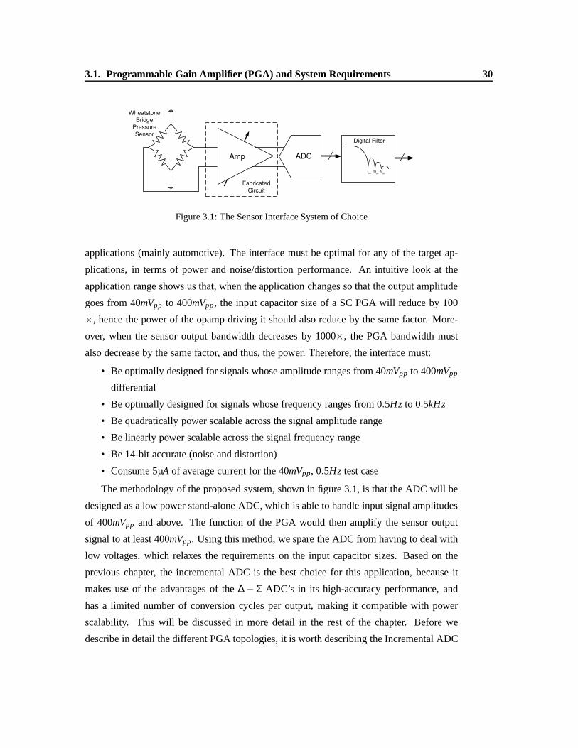
Figure 3.1 shows the system diagram of the sensor interface system that will be designed.
As mentioned above, only the PGA will be designed for this thesis, as indicated in the
dashed box. The PGA will make use of one of the dynamic offset cancelation techniques,
chopping or auto-zeroing, depending on the PGA topology. Inorder to determine what the
design specifications are for the PGA, it is worth reviewing the design specifications for the
entire system, and from that determine the requirements forthe PGA to meet the overall
specifications.
As mentioned in chapter 1, it is desired to reduce their manufacturing costs by mass-
producing a standard interface system that can be used for a number of their pressure sensor
29
3.1. Programmable Gain Amplifier (PGA) and System Requirements 30
Amp ADC
Digital Filter
fch 3f
ch5f
ch
Fabricated
Circuit
Wheatstone
Bridge
Pressure
Sensor
Figure 3.1: The Sensor Interface System of Choice
applications (mainly automotive). The interface must be optimal for any of the target ap-
plications, in terms of power and noise/distortion performance. An intuitive look at the
application range shows us that, when the application changes so that the output amplitude
goes from 40mVpp to 400mVpp, the input capacitor size of a SC PGA will reduce by 100
×, hence the power of the opamp driving it should also reduce bythe same factor. More-
over, when the sensor output bandwidth decreases by 1000×, the PGA bandwidth must
also decrease by the same factor, and thus, the power. Therefore, the interface must:
• Be optimally designed for signals whose amplitude ranges from 40mVpp to 400mVpp
differential
• Be optimally designed for signals whose frequency ranges from 0.5Hz to 0.5kHz
• Be quadratically power scalable across the signal amplitude range
• Be linearly power scalable across the signal frequency range
• Be 14-bit accurate (noise and distortion)
• Consume 5µA of average current for the 40mVpp, 0.5Hz test case
The methodology of the proposed system, shown in figure 3.1, is that the ADC will be
designed as a low power stand-alone ADC, which is able to handle input signal amplitudes
of 400mVpp and above. The function of the PGA would then amplify the sensor output
signal to at least 400mVpp. Using this method, we spare the ADC from having to deal with
low voltages, which relaxes the requirements on the input capacitor sizes. Based on the
previous chapter, the incremental ADC is the best choice forthis application, because it
makes use of the advantages of the∆− Σ ADC’s in its high-accuracy performance, and
has a limited number of conversion cycles per output, makingit compatible with power
scalability. This will be discussed in more detail in the rest of the chapter. Before we
describe in detail the different PGA topologies, it is worthdescribing the Incremental ADC

3.2. Variable Input and Feedback PGA 31
topology that would be used, as this will help determine the target specifications of the
PGA.
3.1.1 Incremental ADC topology
Figure 3.2 below shows the block diagram of a second order incremental ADC with input
feed-forward. As mentioned in the previous chapter, the incremental ADC is modeled as a
∆−Σ ADC with integrators that reset after each conversion cycle[25].
z-1
1- z-1
z-1
1- z-1
1
1- z-1
1
1- z-1++
2
-1
in out
reset reset
Figure 3.2: 2nd-Order Incremental ADC Model with Input Feed-Forward
MATLAB simulations were used to figure out the minimum oversampling ratio that
should be used. figure 3.3 below shows a plot of SQNR Vs OSR for the second order
incremental ADC shown above. The input of the ADC was a 400mVpp signal.
The figure shows that in order to attain 14 bits SQNR, an OSR of at least 250 is required.
Given that the sensor output frequency is a maximum of 0.5kHz, this means that a sampling
frequency of at least 2×0.5kHz×250= 250kHz is needed for a 14−bit incremental ADC.
3.2 Variable Input and Feedback PGA
Several PGA topologies have been suggested in the literature. We will not discuss all the
different architectures, but will go through an overview ofsome of the most significant
ones. Using those architectures as a starting ground, and through discussing the advantages
and disadvantages of each, we will eventually develop a solution that is optimal for our
design application.

3.2. Variable Input and Feedback PGA 32
SQNR Vs OSR
0
20
40
60
80
100
120
1 10 100 1000
OSR
SQ
NR
2nd Order
Figure 3.3: SQNR Vs OSR for the 2nd-Order Incremental ADC Model with Input Feed-Forward
3.2.1 Variable Feedback PGA
Figure 3.4 shows a block diagram of a programmable gain inverting amplifier topology
with variable feedback impedance [26] [27]. We are assumingthat all the designs are
fully differential, although we are representing the single-ended versions for illustration.
Moreover, we are assuming that all amplifiers employ some method of dynamic offset
cancelation technique, whether chopping for continuous time amplifiers, or auto-zeroing
for switched capacitor amplifiers.
+
-
Zin
Zf
Figure 3.4: Programmable Gain Amplifier (Single ended representation) with VariableFeedback Impedance
The variable feedback is implemented by switching in a different series or parallel
combination of resistors or capacitors. The advantage of the above topology is that since
the input impedance is constant, there are no switches at theinput of the system. Input
3.2. Variable Input and Feedback PGA 33
switches are usually a bottle-neck in any switched design because the switch resistance
varies as a function of input. This results in either a gain error, or distortion. Because these
switches are in the feedback network, the effect of variableswitch resistance is reduced by
the gain of the amplifier.
The major disadvantage of this topology is that because the input impedance is constant,
it is not always optimized for noise. Assuming a switched capacitor amplifier was used,
the input referred noise power would be related toKT/C. In a variable feedback PGA
topology, that means that the input capacitor has to be sizedfor the worst case (40mVpp) to
achieve a 14 bit thermal noise level. That means that it wouldbe 100× oversized for the
400mVpp case! The same argument applies in the continuous time amplifier case where the
noise power is a function of 4KT R×NoiseBandwidth. In this case, the input resistor will
be designed for the worst case, which would be 100× undersized for the 400mVpp case.
This inherently makes variable feedback topologies very power inefficient.
Another disadvantage with this topology, is that the power cannot be scaled linearly
with input amplitude to achieve the same opamp bandwidth. Toillustrate this further, let us
consider the closed loop 3dB bandwidth of the opamp:
f3dB =gm
C·β
f3dB =gm
CL +C f //Cin·β
(3.1)
whereCL is the input capacitance of the next stage,Cin andC f are the input and feedback
capacitances, andβ is the beta factor of the gain stage, equal toβ = C f /(C f +Cin). Let us
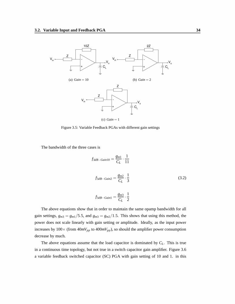
refer to figure 3.5. Assume that thef3dB is chosen to be 10× the chopping frequency. Also,
let us assume that either a single stage amplifier is chosen, or that a two-stage is chosen
where the compensation capacitor (Cc) is a fixed fraction of the load capacitor (CL). CL is
assumed to be the sampling capacitor of the incremental ADC.
3.2. Variable Input and Feedback PGA 34
+
-Z
10Z
CL
Vo
Vin
(a) Gain = 10
+
-Z
2Z
CL
Vo
Vin
(b) Gain = 2
+
-Z
Z
CL
Vo
Vin
(c) Gain = 1
Figure 3.5: Variable Feedback PGAs with different gain settings
The bandwidth of the three cases is
f3dB−Gain10 =gm1
CL·
111
f3dB−Gain2 =gm2
CL·13
f3dB−Gain1 =gm3
CL·12
(3.2)
The above equations show that in order to maintain the same opamp bandwidth for all
gain settings,gm3 = gm1/5.5, andgm3 = gm2/1.5. This shows that using this method, the
power does not scale linearly with gain setting or amplitude. Ideally, as the input power
increases by 100× (from 40mVpp to 400mVpp), so should the amplifier power consumption
decrease by much.
The above equations assume that the load capacitor is dominated byCL. This is true
in a continuous time topology, but not true in a switch capacitor gain amplifier. Figure 3.6
a variable feedback switched capacitor (SC) PGA with gain setting of 10 and 1. in this

3.2. Variable Input and Feedback PGA 35
example, we are assuming that the capacitor “C” is adequately sized to achieve 14 bit noise
floor at 400mVpp input amplitude. Hence, for a 40mVpp input amplitude, “100C” brings the
noise floor to the same 14 bit level. Since the input to the ADC is 400mVpp, Cin,ADC = C
+
-100C
10C
C
Vin
Vo
(a) Input = 40mV , Gain = 10
+
-100C
100C
C
Vin
Vo
(b) Input = 400mV , Gain = 1
Figure 3.6: Variable Feedback SC PGA with different gain settings
The bandwidth of the these cases is
f3dB−Gain10 =gm1
10.1C·
111
=gm1
111.1C
f3dB−Gain1 =gm2
51C·12
=gm2
102C
(3.3)
Equating the two bandwidths( f3dB−Gain10 = f3dB−Gain1), means thatgm1 ≈ gm2. This
result is worse than the continuous time case shown in equation 3.2. This clearly shows
that SC variable feedback PGAs are not suitable for power scalable applications.
3.2.2 Variable Input PGA
One way solve some of the challenges mentioned above is to make the feedback constant,
and change the input impedance of the amplifier, as indicatedin figure 3.7. in this case,
the input is scaled by the gain requirement of the PGA [28] [29]. Because this method
relies on switching different impedances at the input, we fall into the problem of gain
errors and distortion due to signal dependant switch resistance. This can be overcome by
making “impedance-select” switches large enough to reducethe switch resistance. Because
these switches are not being continuously turned on and off,there is no problem of charge
injection associated with large switches. Also, assuming acontinuous-time amplifier is

3.2. Variable Input and Feedback PGA 36
used, the larger the input resistance, the less the effect the switch resistance will have on
the gain accuracy.
+
-
Zin
Zf
Figure 3.7: Programmable Gain Amplifier (Single ended representation) with VariableInput Impedance
Although the above method scales the input impedances according to the gain, they
are still not optimally sized for noise. Referring to figure 3.8, if we were to assume that
the impedance was sized for optimal noise performance at 40mVpp, then in the 200mVpp
case, the impedance should increase by(200/40)2 = 25 times, However, if only the input
impedance changes, then it increases by only a factor of 5. Likewise for the 400mVpp input
case, the impedance increases by a factor of 10 as opposed to the factor of 100 needed.
+
-Z/10
Z
CL
Vin
Vo
(a) Input = 40mV , Gain = 10
CL
+
-Z/2
Z
Vin
Vo
(b) Input = 200mV , Gain = 2
+
-Z
Z
CL
Vin
Vo
(c) Input = 400mV , Gain = 1
Figure 3.8: Variable Input PGAs with different gain settings
In terms of power scalability, the continuous time case willyield the same results as

3.2. Variable Input and Feedback PGA 37
equation 3.2. As for the SC case, figure 3.9 shows an example oftwo gain settings in the
variable feedback case.
+
-100C
10C
C
Vin
Vo
(a) Input = 40mV , Gain = 10
+
-10C
10C
C
Vin
Vo
(b) Input = 400mV , Gain = 1
Figure 3.9: Variable Input SC PGA with different gain settings
In this case, the bandwidth is equal to
f3dB−Gain10 =gm1
10.1C·
111
=gm1
111.1C
f3dB−Gain1 =gm2
6C·12
=gm2
12C
(3.4)
which means that in order to makef3dB−Gain10 = f3dB−Gain1, gm2 = gm1/9.25. Although
this topology scales better than in the previous case, it still does not scale down by the same
factor as the input power.
3.2.3 Variable Input and Feedback PGA
In order to overcome the problem of optimal impedance sizingin relation to the thermal
noise, a proposed method would be to scale both the input and the feedback impedances
[30] [31]. The input impedance is optimally sized accordingto the thermal noise require-
ments, and the feedback is sized according to the gain setting required to produce the
400mVpp minimum output. Figure 3.10 shows the switched capacitor example of a Variable
Input and Feedback PGA. In this case, the capacitor is optimally sized for thermal noise
for both gain settings. This topology will result in both theinput and feedback capacitors
having “impedance select” switches. The effect of those switches is dominated by the input
switches, which we have established in the previous section, is not a problem given proper

3.3. Cascade Gain PGA 38
switch sizing, and thorough simulation.
+
-100C
10C
C
Vin
Vo
(a) Input = 40mV , Gain = 10
+
-C
C
C
Vin
Vo
(b) Input = 400mV , Gain = 1
Figure 3.10: Variable Input and Feedback SC PGA with different gain settings
Let us examine the power scalability of this method. The bandwidths of the two gain
settings are:
f3dB−Gain10 =gm1
10.1C·
111
=gm1
111.1C
f3dB−Gain1 =gm2
1.5C·12
=gm2
3C
(3.5)
which means that in order to makef3dB−Gain10 = f3dB−Gain1, gm2 = gm1/37. Again this is
an improvement over the above two methods, although it stilldoes not scale with the input
power by the same proportion.
With the above analysis, it is worth looking at a different method of designing pro-
grammable gain amplifiers. Rather than switching in different opamps, and impedances,
we will examine Cascaded Gain PGAs.
3.3 Cascade Gain PGA
In this section, we will discuss the Cascaded Gain PGA, and will compare it to the single
stage, variable input and feedback topologies.

3.3. Cascade Gain PGA 39
3.3.1 Cascaded Gain Amplifier with Output Gain Select
Figure 3.11 shows a block diagram of a cascaded gain amplifierwith an output gain select
mux [32] [33]. This means that the gain is set by selecting which amplifieroutput passes
through to the ADC.
Gain SelectMux
Vout
Vin
sel3
sel2
sel1
sel0
X 2.5 X 2 X 2
Figure 3.11: Cascaded Gain stage with output gain select mux
Although this is the most commonly used cascaded gain amplifier, it has many disad-
vantages which are similar to the variable feedback amplifier. Because all signals must pass
through the first amplifier (with the exception of “Gain 1” setting which bypasses all gain
stages), the input impedance is not optimally sized for thermal noise. Moreover, the first
stage opamp must be sized for the worst case, and hence is larger than the others to drive
the next stage’s large capacitance, or resistance . This means that this topology does not
power scale well, since all signals must be amplified by the first, power hungry, amplifier.
This makes this topology very unsuitable for sensor applications.
3.3.2 Cascaded Gain Amplifier with Input Gain Select
Instead of selecting which amplifieroutput should be selected, we propose selecting which
amplifierinput should be selected. Figure 3.12 shows the switched capacitor (3.12(a)) and
continuous time (3.12(b)) versions of the cascaded gain amplifiers with input gain select.
The first amplifier is designed for input signals ranging from40mVpp to 100mVpp, the sec-
ond stage 100mVpp to 200mVpp, and the last stage 200mVpp to 400mVpp. Any signal greater
than 400mVpp would bypass all the stages and output directly into the ADC.Each stage’s

3.3. Cascade Gain PGA 40
input impedance is optimized for the signal power that it is meant to amplify. In these two
diagrams, we are assuming that “C” is the capacitance neededto bring the thermal noise
floor 14 bit below the 400mVpp signal, and “R” is the resistance needed to bring the noise
14 bit below the 40mVpp signal. Req,ADC is the equivalent input resistance of the input ca-
pacitance of the ADC that follows the PGA, and is equal toReq,ADC = 1/( fs ×Cs). Similar
to the variable input and feedback amplifier, the input impedances become optimally sized
for thermal noise.
+
-
100C
40C
+
-
16C
8C
+
-
2C
4CInput Mux
(GainSelect)
Vout
Vin
pd3pd3
pd2pd2
pd1pd1I
I/6I/24
sel3
sel2
sel1
sel0
CADC
= C
(a) Switched Capacitor
+
-
R
2.5R
+
-
6R
12R
+
-
48R
24RInput Mux
(GainSelect)
Vout
Vin
pd3pd3
pd2pd2
pd1pd1I
I/6I/24
sel3
sel2
sel1
sel0
Req,ADC
= 1/(fs x C
ADC)
(b) Continuous Time
Figure 3.12: Cascaded Switched Capacitor Amplifier with Input Gain Select Mux
Now let us examine the power scalability of this topology. For the switched capacitor
case in Fig. 3.12(a), the closed loop bandwidth of the amplifiers is given by:
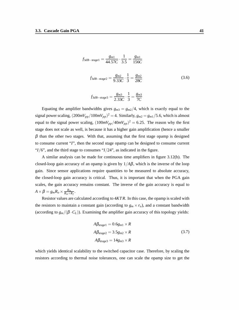
3.3. Cascade Gain PGA 41
f3dB−stage1 =gm1
44.57C·
13.5
=gm1
156C
f3dB−stage2 =gm2
9.33C·13
=gm2
28C
f3dB−stage3 =gm3
2.33C·13
=gm3
7C
(3.6)
Equating the amplifier bandwidths givesgm3 = gm2/4, which is exactly equal to the
signal power scaling,(200mVpp/100mVpp)2 = 4. Similarly,gm2 = gm1/5.6, which is almost
equal to the signal power scaling,(100mVpp/40mVpp)2 = 6.25. The reason why the first
stage does not scale as well, is because it has a higher gain amplification (hence a smaller
β than the other two stages. With that, assuming that the first stage opamp is designed
to consume current “I”, then the second stage opamp can be designed to consume current
“ I/6”, and the third stage to consumes “I/24”, as indicated in the figure.
A similar analysis can be made for continuous time amplifiersin figure 3.12(b). The
closed-loop gain accuracy of an opamp is given by 1/Aβ , which is the inverse of the loop
gain. Since sensor applications require quantities to be measured to absolute accuracy,
the closed-loop gain accuracy is critical. Thus, it is important that when the PGA gain
scales, the gain accuracy remains constant. The inverse of the gain accuracy is equal to
A×β = gmRo × RinRin+R f
.
Resistor values are calculated according to 4KT R. In this case, the opamp is scaled with
the resistors to maintain a constant gain (according togm × ro), and a constant bandwidth
(according togm/(β ·CL)). Examining the amplifier gain accuracy of this topology yields:
Aβstage1 = 0.6gm1×R
Aβstage2 = 3.5gm2×R
Aβstage3 = 14gm3×R
(3.7)
which yields identical scalability to the switched capacitor case. Therefore, by scaling the
resistors according to thermal noise tolerances, one can scale the opamp size to get the

3.3. Cascade Gain PGA 42
same opamp gain and bandwidth.
From the above above topologies, it becomes apparent that the cascaded gain amplifier
with input gain select is the best for automotive sensor applications. The question still
remains as to whether switched capacitor, or continuous time topology should be used.
3.3.3 Switched Cap Vs Continuous Time PGA’s
In order to figure out whether switched capacitor or continuous time PGA should be used,
we should better understand the interaction between the sensor and the PGA. Because the
sensor is a piezoresistive one, it has a finite output resistance. This means that if a switched
capacitor topology is used, theRC time constant may be too large for the sensor output
signal to settle. In a continuous time topology, the input resistance of the amplifier may be
too small, which will in effect reduce the gain of the first amplifier in the cascade. In either
case, the sizes of the input resistance and capacitors play arole in determining which will
be used. for that we need to analyze both topologies from a thermal noise perspective.
Thermal Noise Considerations
Figure 3.13 shows the switched capacitor amplifier which waspresented in the previous
section as the auto-zeroing amplifier.
-
+
C1
C2
Vin
Vout
VOS
+
-
2
21
1
1
Figure 3.13: Switched capacitor amplifier
Where the gainG of the amplifier isC2/C1. The input referred noise due to the switch-
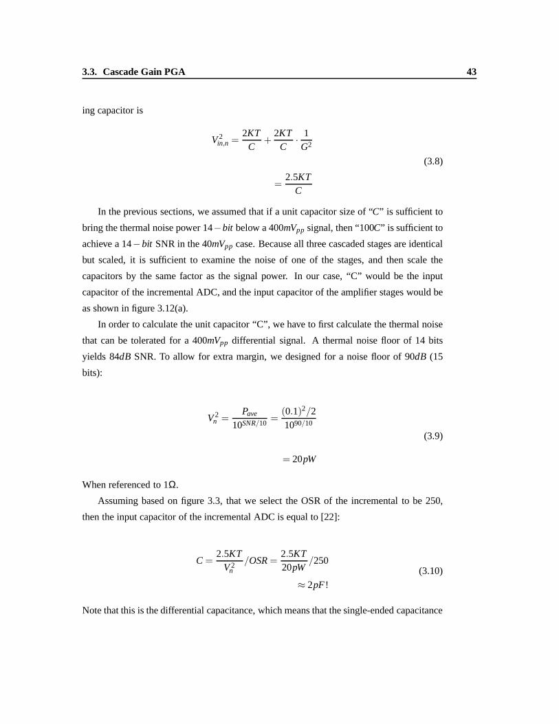
3.3. Cascade Gain PGA 43
ing capacitor is
V 2in,n =
2KTC
+2KT
C·
1G2
=2.5KT
C
(3.8)
In the previous sections, we assumed that if a unit capacitorsize of “C” is sufficient to
bring the thermal noise power 14−bit below a 400mVpp signal, then “100C” is sufficient to
achieve a 14−bit SNR in the 40mVpp case. Because all three cascaded stages are identical
but scaled, it is sufficient to examine the noise of one of the stages, and then scale the
capacitors by the same factor as the signal power. In our case, “C” would be the input
capacitor of the incremental ADC, and the input capacitor ofthe amplifier stages would be
as shown in figure 3.12(a).
In order to calculate the unit capacitor “C”, we have to first calculate the thermal noise
that can be tolerated for a 400mVpp differential signal. A thermal noise floor of 14 bits
yields 84dB SNR. To allow for extra margin, we designed for a noise floor of90dB (15
bits):
V 2n =
Pave
10SNR/10=
(0.1)2/2
1090/10
= 20pW
(3.9)
When referenced to 1Ω.
Assuming based on figure 3.3, that we select the OSR of the incremental to be 250,
then the input capacitor of the incremental ADC is equal to [22]:
C =2.5KT
V 2n
/OSR =2.5KT20pW
/250
≈ 2pF !
(3.10)
Note that this is the differential capacitance, which meansthat the single-ended capacitance

3.3. Cascade Gain PGA 44
is 2× 2pF = 4pF , which means that the total capacitance is equal to 8pF . That means
that the input of the first stage of the cascaded amplifier willbe 100C = 800pF ! which is
impractical for fabrication. By increasing the OSR to 1000,the capacitorC = 2pF . By
making theOSR = 5000,C can be made equal to 400f F , which is a reasonable size for
the input capacitor of a low power ADC. The input to the amplifier will still be equal to
100C = 40pF , which is still pretty large, but not impractical for fabrication. going to higher
oversampling ratios will not be practical, as that would mean increasing the bandwidth of
the operational amplifiers by the OSR, and hence the power. Depending on the size of
the output resistance of the piezoresistive sensor, it may not be practical to load it with a
switch capacitor amplifier with such a large input capacitor. This makes switched capacitor
amplifiers unattractive for resistive based sensors.
Let us examine the continuous time amplifier stages with froma thermal noise perspec-
tive. Figure 3.14 shows the noise model of the continuous time inverting amplifier.
+
-
Vn1
R2
*
*R
1
Vn2
Vo
Vin
Figure 3.14: Noise model of Inverting R-amplifier
Based on the resistor noise model, we can derive the output noise power of the contin-
uous time amplifier as being [34]:
V 2out,n = 4KT R1×
(
R1
R2
)2
× fNBW +4KT R2× fNBW (3.11)
where fNBW = f3dB ·π/2. When referred to the input, the thermal noise becomes
V 2in,n = 4KT R1× fNBW +4KT R2×
(
R2
R1
)2
× fNBW (3.12)
The above formulas show that there is a dependance on not onlythe input resistance,

3.3. Cascade Gain PGA 45
but also on the 3dB bandwidth of the closed loop amplifier. To calculate the input resistance
required to achieve 14−bits noise floor for a 40mVpp signal, we get
V 2n =
Pave
10SNR/10=
(0.02)2/2
1090/10
= 200fW
(3.13)
Therefore, the value forR1 can be calculated in a similar way toC. Assuming that the
OSR = 5000, then the ADC sampling frequency is equal to 2× 0.5kHz×OSR = 5MHz.
Assume that thef3dB of the amplifier is equal to 5× the ADC sampling frequency, thenR1
can be calculated to be
R1 ≤V 2
n
4KT × fNBW×OSR =
200W4KT × f3dBπ/2
×5000
≈ 1.5kΩ
(3.14)
This resistor value is too small to be the input resistance ofthe amplifier, considering
that the output resistance of the sensor is in the order of kilo-Ohms. We cannot arbitrarily
increase the resistance without reducing the effective noise bandwidth. We can see that by
reducing the noise bandwidth,fNBW , of the amplifier, we can increase that resistance, how-
ever, we would run into settling issues, as well as degraded residual offset due to chopping.
It is clear from the above two examples that the ideal topology for the gain stages is
one where the input resistance can be increased arbitrarilywithout affecting the noise. The
larger the input resistance, the less the effect of the variable resistance (due to the sensor
and switches) will have on the amplifier. The problem with thetopology above is that
the because we are following a continuous-time system with asampled system, the out-
of-band noise will alias back in-band, which increases the in-band noise. This makes an
anti-aliasing filter necessary for the above topology.
An active RC amplifier solves the above two problems of anti-aliasing, and R-dependance.
Let us examine the noise model of the RC-Amplifier shown in figure 3.15. Analyzing the
output noise power of the amplifier, we get

3.3. Cascade Gain PGA 46
Vin
+
-
Vn1
R2
C
*
*R
1
Vn2
Vo
Figure 3.15: Noise Model of active RC stage
V 2out,n = 4KT R1× (H1(s))
2 +4KT R2× (H2(s))2 (3.15)
where,
H1(s) =R2/R1
1+ R2Cs(3.16)
and,
H2(s) =1
1+ R2Cs(3.17)
combining 3.15, with 3.16 and 3.17, results in
V 2out,n = 4KT R1×
(
R2
R1
)2
×1
4R2C+4KT R2×
14R2C
=
(
1+R2
R1
)
×KTC
(3.18)
Which is independent ofR1. It is dependant only on the value of the gain(R1/R2), and the
value of “C”. Because this topology allows us to choose a highvalue for “R”, the gain of
the amplifier is not affected by the output impedance of the sensor. This means that this
topology has a higher gain accuracy than the previous topologies.
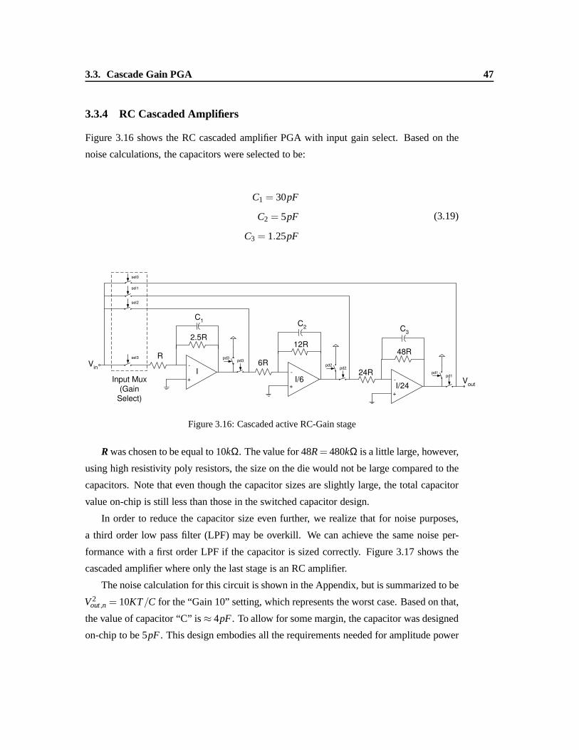
3.3. Cascade Gain PGA 47
3.3.4 RC Cascaded Amplifiers
Figure 3.16 shows the RC cascaded amplifier PGA with input gain select. Based on the
noise calculations, the capacitors were selected to be:
C1 = 30pF
C2 = 5pF
C3 = 1.25pF
(3.19)
+
-
R
2.5R
+
-
6R
12R
+
-
48R
24R
C3
Input Mux(Gain
Select)
sel3
sel2
sel1
sel0
Vout
Vin
pd3pd3
pd2pd2
pd1pd1I
I/6I/24
C2
C1
Figure 3.16: Cascaded active RC-Gain stage
R was chosen to be equal to 10kΩ. The value for 48R = 480kΩ is a little large, however,
using high resistivity poly resistors, the size on the die would not be large compared to the
capacitors. Note that even though the capacitor sizes are slightly large, the total capacitor
value on-chip is still less than those in the switched capacitor design.
In order to reduce the capacitor size even further, we realize that for noise purposes,
a third order low pass filter (LPF) may be overkill. We can achieve the same noise per-
formance with a first order LPF if the capacitor is sized correctly. Figure 3.17 shows the
cascaded amplifier where only the last stage is an RC amplifier.
The noise calculation for this circuit is shown in the Appendix, but is summarized to be
V 2out,n = 10KT/C for the “Gain 10” setting, which represents the worst case. Based on that,
the value of capacitor “C” is≈ 4pF. To allow for some margin, the capacitor was designed
on-chip to be 5pF . This design embodies all the requirements needed for amplitude power
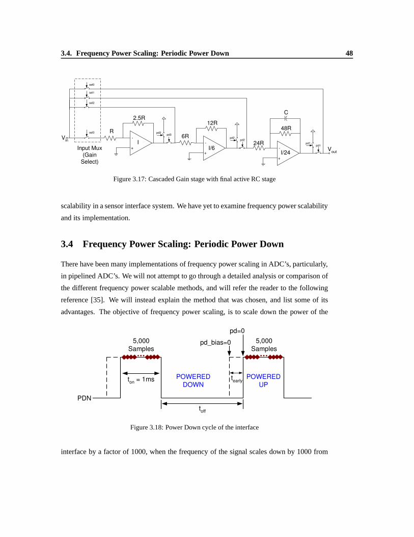
3.4. Frequency Power Scaling: Periodic Power Down 48
+
-
R
2.5R
+
-
6R
12R
+
-
48R
24R
C
Input Mux(Gain
Select)
Vout
Vin
pd3pd3
pd2pd2
pd1pd1I
I/6I/24
sel3
sel2
sel1
sel0
Figure 3.17: Cascaded Gain stage with final active RC stage
scalability in a sensor interface system. We have yet to examine frequency power scalability
and its implementation.
3.4 Frequency Power Scaling: Periodic Power Down
There have been many implementations of frequency power scaling in ADC’s, particularly,
in pipelined ADC’s. We will not attempt to go through a detailed analysis or comparison of
the different frequency power scalable methods, and will refer the reader to the following
reference [35]. We will instead explain the method that was chosen, and list some of its
advantages. The objective of frequency power scaling, is toscale down the power of the
POWERED
DOWN
POWERED
UP
PDN
5,000
Samples
5,000
Samples
ton
= 1ms
pd_bias=0
pd=0
toff
tearly
Figure 3.18: Power Down cycle of the interface
interface by a factor of 1000, when the frequency of the signal scales down by 1000 from

3.4. Frequency Power Scaling: Periodic Power Down 49
0.5kHz to 0.5Hz. The basic principle of the selected method of power scaling, is that,
instead of scaling down the current and clock frequency of the interface and ADC, the
entire interface is powered down for a period of time. That effectively reduces the average
power consumption by the same amount as the Power Down (PD) factor. Figure 3.18
illustrates the power down cycle of our design. If the interface was on fortON , and off for
tOFF , then the power down factor would be
PD =tOFF + tON
tON(3.20)
and the average power would be:
Pavg = PON ·tON
tON + tOFF=
PON
PD(3.21)
We designed the interface so that in the 0.5kHz case, the system is never powered
down, and in the 0.5Hz case, the interface and ADC have a PD factor of 1000. Since
the system is oversampled by 5000, this leads to an ADC sampling clock frequency of
2×0.5kHz×5000= 5MHz. This means that the interface is always turned on fortON =
1ms, and tOFF varies depending on the frequency of the input signal. This makes the
effective sampling rate of the ADC equal to:
Fs,e f f ective =Fs
PD(3.22)
Which means that the effective OSR is maintained regardlessof the input frequency. For
the 0.5Hz case (PD = 1000), the OSR is equal toFs,e f f ective/(2× f in).
In figure 3.18, we have shown that there are two ”power up” signals, with a time dif-
ference oftEARLY . This is to allow crucial parts of the circuits, such as opampbias circuits
to be powered up and ready before the rest of the interface andADC are powered up. The
power down control was implemented by programming a finite state machine (FSM) on an
FPGA board.

Chapter 4
Circuit Level Implementation and Simulations
In this chapter, we will discuss the circuit level implementation of our sensor interface
system that was presented in the previous chapter. We will discuss the opamp topologies
used in the interface design, and circuit implementation ofpower-down techniques used.
We will then discuss the buffer stage that was used after the interface. The chopper clock
generation techniques will also be presented. Finally, we will discuss design for testability,
and present its implementation in our design.
4.1 Operational Amplifiers
As discussed in chapter 2, because sensor applications dealwith very slow signals, dynamic
offset and 1/F noise cancelation techniques are necessary in order to achieve high accu-
racy. We have discussed different implementations, such asauto-zeroing and chopping.
Since our interface implementation uses continuous-time amplifier stages, chopping is the
technique of choice. In our design, we will use the two-stagechopper amplifier, with the
demodulation chopper after the first stage. We have discussed this topology in chapter 2,
and in figure 4.1, we re-show the two-stage amplifier of choice.
For this application, a two stage amplifier was better than a single stage one because it
has a higher gain, and hence a better gain accuracy. The chopping frequency was selected to
be 1/2 of the ADC sampling frequency,fchop = 2.5MHz. In chapter 2, we have discussed
how the above architecture is suitable for high chopping frequencies.
50

4.1. Operational Amplifiers 51
A1 A2+
-
+
-
-
+
-
+V
inV
out
Cc
Cc
Ri
Ri
Rf
Rf
chch
+-
VOS1
+-
VOS2
Figure 4.1: The two-stage chopper amplifier
4.1.1 Opamp Topology and Sizes
Figure 4.2 shows the circuit implementation of the fully differential opamp shown in figure
4.1. The architecture presented is based the Power Resettable Opamp (PROpamp) shown
in [35], although in the reference, the opamp used was a gain boosted folded cascode opamp
[36] as opposed to a two-stage one presented in here.
vinp1vinn1
vbp1
vp
vbpcasc vbp
casc
vbncascvbn
casc
vn
0.9V 0.9V
vbp1
vop
0.9V
vo
n
vcntrl
0.9V
vcntrl
vbp1
pdn
pdn
pd
pdpdn
pdn
vp1 vn1
M1 M2
M4 M7M6 M5
M8 M9
M10 M11
M12 M13
M14 M15
M17M16
M3
MSW1
MSW2
MSW3
MSW4
MSW5 M
SW6
RC
CC
CC
RC
MSW7
chop_clk chop_clkn
vinn
vinp
vinn1
vinp1
chop_clki chop_clknichop_clk chop_clkn
vn
vp
vn1
vp1
chop_clki chop_clkni
Figure 4.2: two-stage chopped Opamp circuit diagram
Table 4.1 shows the transistor and component sizing for the three stages in the opamp.
The transistor lengths used were larger than the minimum size in order to reduce the 1/F
noise effect by increasing the area. PMOS input transistorsare often used in sensor ap-
plications because they exhibit better 1/F noise performance. As was stated in chapter

4.1. Operational Amplifiers 52
2, 1/F noise comes from the trapped carriers in the gate oxide. Since the PMOS carriers
(holes) are larger then the NMOS carriers (electrons), theyare less likely to get trapped and
gradually released.
Table 4.1: Opamp Transistor Sizing for the three stage cascade amplifier
Component First Stage Second Stage Third StageName Sizing Sizing Sizing
M1,M2 96×2/0.25 16×2/0.25 4×2/0.25M3 48×4/0.50 8×4/0.50 2×4/0.50M4−M7 24×1/0.50 4×1/0.50 1×1/0.50M8,M9 24×1/0.50 4×1/0.50 1×1/0.50M10−M13 24×4/0.50 4×4/0.50 1×4/0.50M14,M15 56×1/0.50 8×1/0.50 4×1/0.50M16,M17 52×4/0.50 8×4/0.50 4×4/0.50MSW1,MSW2 8×2/0.18 4×2/0.18 1×2/0.18MSW3,MSW4 20×2/0.18 10×2/0.18 4×2/0.18MSW5,MSW6 60×2/0.18 30×2/0.18 8×2/0.18MSW7 26×4/0.18 12×4/0.18 4×4/0.18RC 1kΩ 4kΩ 5kΩCC 6pF 1.2pF 900f F
Table 4.1 also shows how the opamp transistors scale with theinput signal power.RC
is a lead compensation resistor and is sized to optimize the phase margin of the amplifiers.
The amplifiers were designed to achieve a gain of approximately 80dB, and a band-
width of approximately 25MHz, which is 10× the chopping frequency. The AC simulation
parameters of the opamps are presented in table 4.2.
Table 4.2: AC Simulation Parameters for the Three Amplifiers
Parameter First Stage Second Stage Third Stage
Aβ 82.2dB 81.7dB 80.9dBβ ·Ft 25MHz 23MHz 23MHzPhaseMargin 88o 68o 77o
CurrentConsumption 2.14mA 319.72µA 121.72µA

4.1. Operational Amplifiers 53
4.1.2 Common Mode Feedback (CMFB)
TransistorsM4− M7 in figure 4.2 form the common-mode feedback for the first stage
of the opamp, known as the “inherent common mode feedback” [37]. Due to stability
considerations, a two-stage fully differential opamp is usually designed with two common-
mode feedback stages, one for each stage. This is increases power consumption, which
is unwanted in low power sensor design. The “inherent commonmode feedback” struc-
ture eliminates the need for a specialized CMFB circuit. Itsbasic operating principle is
that the cascoded current source is split into two equally sized sources, and the gates are
cross coupled at the differential output of the first stage toform a negative feedback. The
output impedance seen by the differential signal is high, limited by the output impedance
of the PMOS cascoded load. The common mode impedance, however, is dominated by
(gmM4 + gmM6) and(gmM5 + gmM7). Because of this low common mode impedance, the
cross coupled feedback structure is sufficient and there is not need for an additional CMFB
circuit [37] [38].
The second stage of the opamp, which is a Class A common-source output stage, re-
quires its own common mode feedback circuitry, shown in figure 4.3. Since the amplifiers
are continuous time, the output is always expected to be available, and so is the common
mode, hence a continuous time common mode structure was used. The circuit senses the
output common mode voltage of the opamp through resistorsRCM, and compares it to an
off-chip common mode level,vcmoc. The relative current in the branches is then steered
either way to produce a common mode control voltage,vcntrl, that feeds into the current
source of the output stage.
Similar to the opamp, the CMFB circuit was scaled in size by the same factor as the
opamp whose common mode it controls. Table 4.3 shows the sizing of the CMFB circuit
in the three amplifier stages.
RCM was selected at a relatively high value so that the output impedance would not be
affected, hence reducing the gain of the amplifier.
4.1.3 Chopper Switches
The chopper switches were implemented using transmission gates, such as the ones shown
in figure 4.4.

4.1. Operational Amplifiers 54
vbn
pdn
vcm_oc
vcntrloutn
outp
Rcm
Rcm
MSW1
M1 M2
M3
M4 M5
Figure 4.3: CMFB circuit
Table 4.3: CMFB Transistor Sizing for the three stage cascade amplifier
Transistor First Stage Second Stage Third StageName Sizing Sizing Sizing
M1,M2 96×2/0.25 16×2/0.25 4×2/0.25M3 48×4/0.50 8×4/0.50 2×4/0.50M4,M5 24×1/0.50 4×1/0.50 1×1/0.50RCM 100kΩ 200kΩ 200kΩ
=>
MPSW
MNSW
S
Si
Figure 4.4: Chopper switch implementation: transmission gate
The sizings of the switches are shown in table 4.4. Since the input chopper are on the
virtual ground node, there is no signal component, and hencethe transistors are minimum
sized. Since the output choppers contain some signal component (although still small,
equal toVout/A2), the transistors are sized 5 times the minimum. This sized was optimized
to produce the best distortion performance after simulation.
4.1.4 Bias Circuit Power Down
The first amplifier stage has its own bias circuit, whereas thesecond and third stage both
share a bias circuit. Because the opamps are periodically powered down due to power
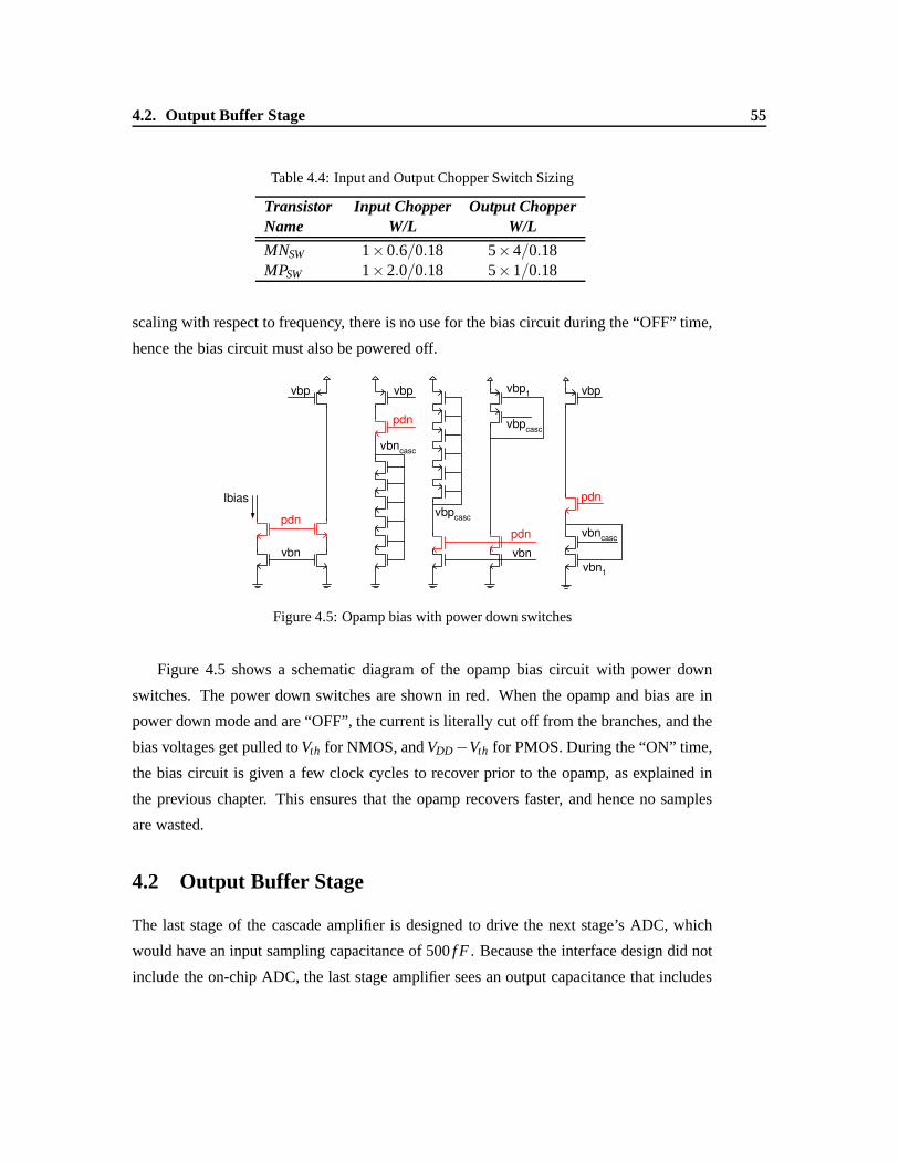
4.2. Output Buffer Stage 55
Table 4.4: Input and Output Chopper Switch Sizing
Transistor Input Chopper Output ChopperName W/L W/L
MNSW 1×0.6/0.18 5×4/0.18MPSW 1×2.0/0.18 5×1/0.18
scaling with respect to frequency, there is no use for the bias circuit during the “OFF” time,
hence the bias circuit must also be powered off.
Ibias
pdn
vbn vbn
pdn
vbp vbp vbp
pdn
vbncasc
pdn
vbpcasc
vbpcasc
vbncasc
vbp1
vbn1
Figure 4.5: Opamp bias with power down switches
Figure 4.5 shows a schematic diagram of the opamp bias circuit with power down
switches. The power down switches are shown in red. When the opamp and bias are in
power down mode and are “OFF”, the current is literally cut off from the branches, and the
bias voltages get pulled toVth for NMOS, andVDD −Vth for PMOS. During the “ON” time,
the bias circuit is given a few clock cycles to recover prior to the opamp, as explained in
the previous chapter. This ensures that the opamp recovers faster, and hence no samples
are wasted.
4.2 Output Buffer Stage
The last stage of the cascade amplifier is designed to drive the next stage’s ADC, which
would have an input sampling capacitance of 500f F . Because the interface design did not
include the on-chip ADC, the last stage amplifier sees an output capacitance that includes
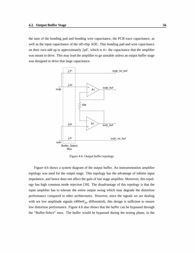
4.2. Output Buffer Stage 56
the sum of the bonding pad and bonding wire capacitance, the PCB trace capacitance, as
well as the input capacitance of the off-chip ADC. This bonding pad and wire capacitance
on their own add up to approximately 2pF , which is 4× the capacitance that the amplifier
was meant to drive. This may lead the amplifier to go unstable unless an output buffer stage
was designed to drive that large capacitance.
A1
A1
20k
+
-
-
+
B1
B1
B2
B2
Buffer_SelectMux
outp_buf
outn_buf
outn_no_buf
outp_no_buf
outp
outn
Figure 4.6: Output buffer topology
Figure 4.6 shows a system diagram of the output buffer. An instrumentation amplifier
topology was used for the output stage. This topology has theadvantage of infinite input
impedance, and hence does not affect the gain of last stage amplifier. Moreover, this topol-
ogy has high common mode rejection [39]. The disadvantage ofthis topology is that the
input amplifier has to tolerate the entire output swing whichmay degrade the distortion
performance compared to other architectures. However, since the signals we are dealing
with are low amplitude signals (400mVpp differential), this design is sufficient to ensure
low distortion performance. Figure 4.6 also shows that the buffer can be bypassed through
the “Buffer-Select” mux. The buffer would be bypassed during the testing phase, in the

4.2. Output Buffer Stage 57
case where we would like to verify the output common mode of the PGA.
vinp1vinn1
vp1
vp
vbpcasc
vbpcasc
vbncascvbn
casc
vn
vp1
vo
p
vbp1
vn1
vbn1 vbn1 vbn1
M1 M2
M3
M4 M5
M6 M7
M8 M9
M10 M11
M12
M13
CC
RC
chop_clk chop_clkn
vinn
vinp
vinn1
vinp1
chop_clki chop_clknichop_clk chop_clkn
vn
vp
vn1
vp1
chop_clki chop_clkni
Figure 4.7: Buffer Opamp circuit
Figure 4.7 shows the circuit implementation of one of the buffer opamps. The design
is a differential-to-single-ended two-stage opamp with a PMOS folded cascode as a first
stage and a class-A common source output stage. This amplifier is also chopped to reduce
its offset and 1/F noise contribution. Because the input differential pairs experience the
full signal swing, the input choppers have to be sized appropriately. In this case, both the
input and output choppers were designed to be 5× the minimum size switches.
Table 4.5: Opamp Transistor Sizing for the three stage cascade amplifier
Component ComponentName Sizing
M1,M2 88×2/0.25M3 48×4/0.50M4,M5 48×1/0.50M6,M7 24×1/0.50M8−M11 24×4/0.50M12 216×1/0.50M13 216×4/0.50RC 100ΩCC 15pF
Table 4.5 shows the transistor sizes of the buffer opamp. Theopamp was designed to
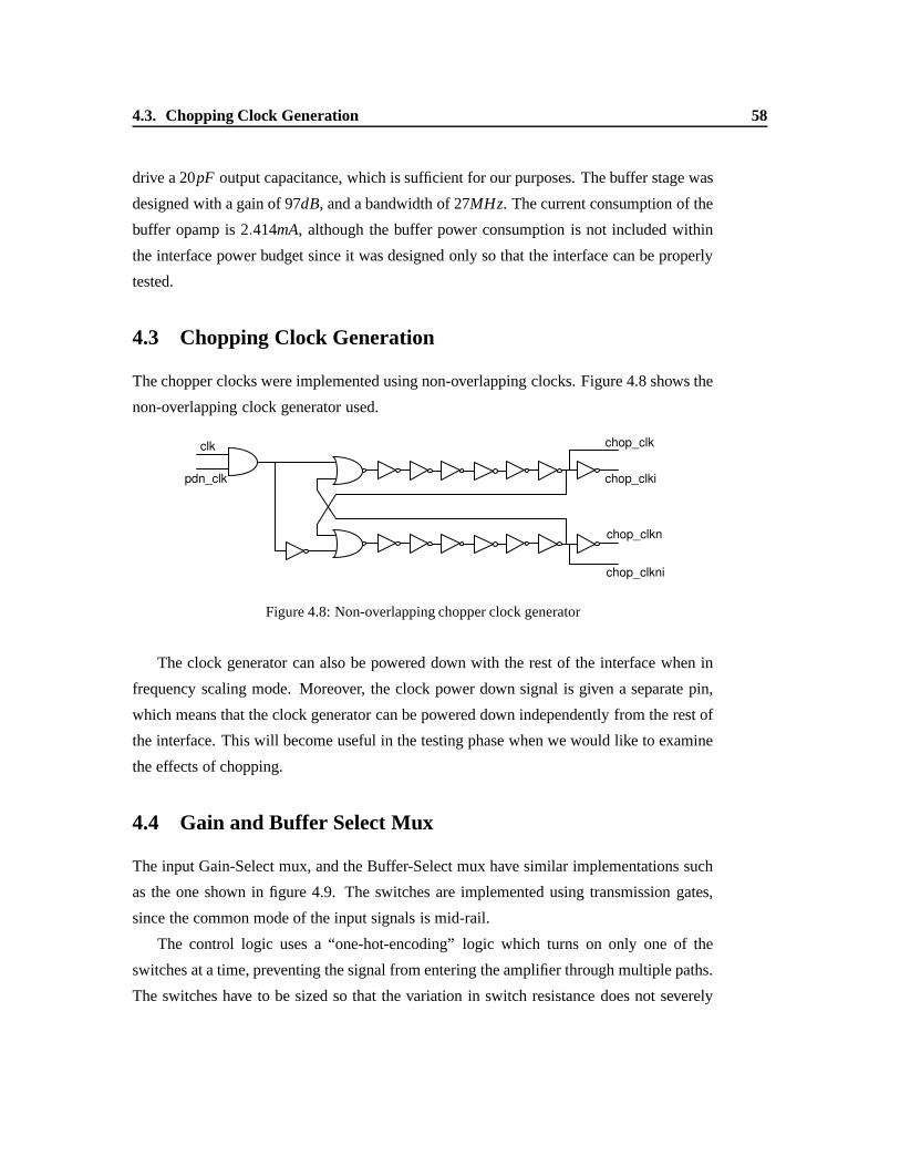
4.3. Chopping Clock Generation 58
drive a 20pF output capacitance, which is sufficient for our purposes. The buffer stage was
designed with a gain of 97dB, and a bandwidth of 27MHz. The current consumption of the
buffer opamp is 2.414mA, although the buffer power consumption is not included within
the interface power budget since it was designed only so thatthe interface can be properly
tested.
4.3 Chopping Clock Generation
The chopper clocks were implemented using non-overlappingclocks. Figure 4.8 shows the
non-overlapping clock generator used.
clk
pdn_clk
chop_clk
chop_clki
chop_clkn
chop_clkni
Figure 4.8: Non-overlapping chopper clock generator
The clock generator can also be powered down with the rest of the interface when in
frequency scaling mode. Moreover, the clock power down signal is given a separate pin,
which means that the clock generator can be powered down independently from the rest of
the interface. This will become useful in the testing phase when we would like to examine
the effects of chopping.
4.4 Gain and Buffer Select Mux
The input Gain-Select mux, and the Buffer-Select mux have similar implementations such
as the one shown in figure 4.9. The switches are implemented using transmission gates,
since the common mode of the input signals is mid-rail.
The control logic uses a “one-hot-encoding” logic which turns on only one of the
switches at a time, preventing the signal from entering the amplifier through multiple paths.
The switches have to be sized so that the variation in switch resistance does not severely
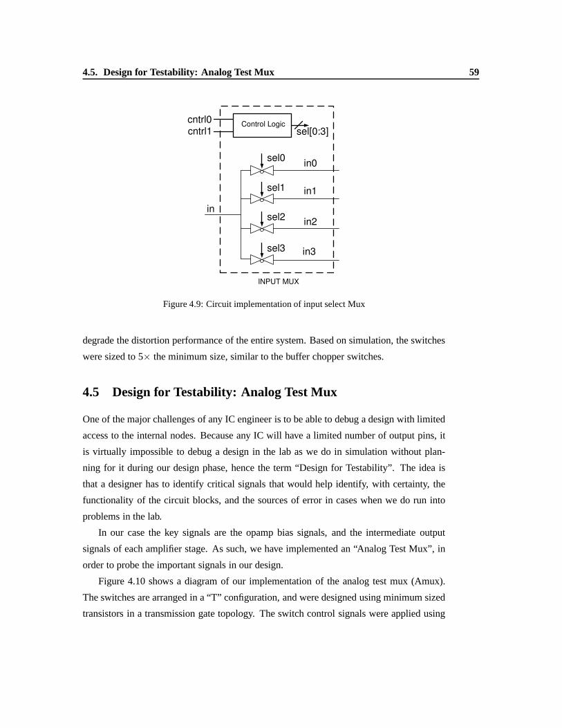
4.5. Design for Testability: Analog Test Mux 59
Control Logic
sel0
sel1
sel2
sel3
in0
in1
in2
in3
in
sel[0:3]cntrl0cntrl1
INPUT MUX
Figure 4.9: Circuit implementation of input select Mux
degrade the distortion performance of the entire system. Based on simulation, the switches
were sized to 5× the minimum size, similar to the buffer chopper switches.
4.5 Design for Testability: Analog Test Mux
One of the major challenges of any IC engineer is to be able to debug a design with limited
access to the internal nodes. Because any IC will have a limited number of output pins, it
is virtually impossible to debug a design in the lab as we do insimulation without plan-
ning for it during our design phase, hence the term “Design for Testability”. The idea is
that a designer has to identify critical signals that would help identify, with certainty, the
functionality of the circuit blocks, and the sources of error in cases when we do run into
problems in the lab.
In our case the key signals are the opamp bias signals, and theintermediate output
signals of each amplifier stage. As such, we have implementedan “Analog Test Mux”, in
order to probe the important signals in our design.
Figure 4.10 shows a diagram of our implementation of the analog test mux (Amux).
The switches are arranged in a “T” configuration, and were designed using minimum sized
transistors in a transmission gate topology. The switch control signals were applied using
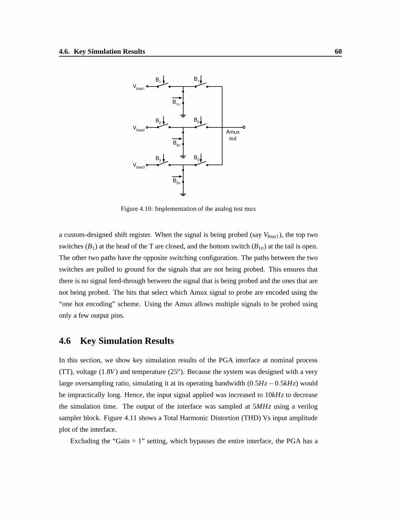
4.6. Key Simulation Results 60
B1
B1
B1n
B2
B2
B2n
B3
B3
B3n
Vbias2
Vbias1
Vbias3
Amuxout
Figure 4.10: Implementation of the analog test mux
a custom-designed shift register. When the signal is being probed (sayVbias1), the top two
switches (B1) at the head of the T are closed, and the bottom switch (B1n) at the tail is open.
The other two paths have the opposite switching configuration. The paths between the two
switches are pulled to ground for the signals that are not being probed. This ensures that
there is no signal feed-through between the signal that is being probed and the ones that are
not being probed. The bits that select which Amux signal to probe are encoded using the
“one hot encoding” scheme. Using the Amux allows multiple signals to be probed using
only a few output pins.
4.6 Key Simulation Results
In this section, we show key simulation results of the PGA interface at nominal process
(TT), voltage (1.8V ) and temperature (25o). Because the system was designed with a very
large oversampling ratio, simulating it at its operating bandwidth (0.5Hz−0.5kHz) would
be impractically long. Hence, the input signal applied was increased to 10kHz to decrease
the simulation time. The output of the interface was sampledat 5MHz using a verilog
sampler block. Figure 4.11 shows a Total Harmonic Distortion (THD) Vs input amplitude
plot of the interface.
Excluding the “Gain = 1” setting, which bypasses the entire interface, the PGA has a
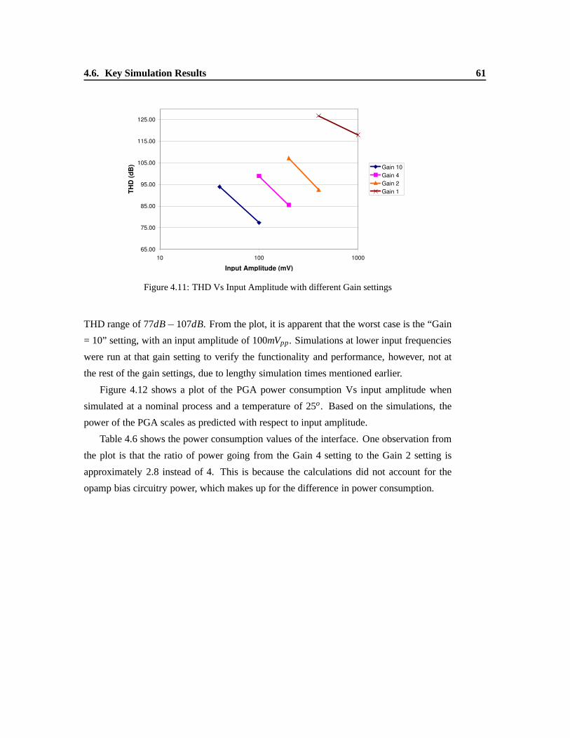
4.6. Key Simulation Results 61
65.00
75.00
85.00
95.00
105.00
115.00
125.00
10 100 1000
Input Amplitude (mV)
TH
D (
dB
) Gain 10
Gain 4
Gain 2
Gain 1
Figure 4.11: THD Vs Input Amplitude with different Gain settings
THD range of 77dB−107dB. From the plot, it is apparent that the worst case is the “Gain
= 10” setting, with an input amplitude of 100mVpp. Simulations at lower input frequencies
were run at that gain setting to verify the functionality andperformance, however, not at
the rest of the gain settings, due to lengthy simulation times mentioned earlier.
Figure 4.12 shows a plot of the PGA power consumption Vs inputamplitude when
simulated at a nominal process and a temperature of 25o. Based on the simulations, the
power of the PGA scales as predicted with respect to input amplitude.
Table 4.6 shows the power consumption values of the interface. One observation from
the plot is that the ratio of power going from the Gain 4 setting to the Gain 2 setting is
approximately 2.8 instead of 4. This is because the calculations did not account for the
opamp bias circuitry power, which makes up for the difference in power consumption.

4.6. Key Simulation Results 62
0.010
0.100
1.000
10.000
10 100 1000
Input Amplitude (mV)
Po
we
r (m
W)
PD0
Gain 10Gain 4
Gain 2
Gain 1
Figure 4.12: Power Vs Input Amplitude
Table 4.6: Simulated Power Consumption
Input Amplitude Gain Power Consumption(mVpp) Setting (mW )
40 10 5.278100 10 5.278101 4 0.984200 4 0.984201 2 0.349400 2 0.349401 1 0.0011000 1 0.001

Chapter 5
Experimental Results
I N this section, we discuss the experimental results of the power scalable PGA, which
was fabricated in 0.18µm CMOS process. In section 5.2, we discuss the Test setup in
detail as well as the test methodology used to characterize the PGA. In section 5.3 and 5.4,
we characterize the signal generator, and the off-chip ADC used to capture data from the
PGA. The purpose of these tests is to establish with certainty the maximum performance
that can be captured from the entire system, since the performance can potentially be lim-
ited by setup, and not by the PGA itself. In section 5.5, we present and explain the test
results of the fabricated PGA. The PGA was able to achieve a dynamic range of 80dB (13
bits), and a noise distribution of 170nV /√
Hz with chopping. Power scalability with respect
to input amplitude was done by running the PGA with a wide range of input amplitudes
(40mVpp -1Vpp), and varying the gain accordingly to get a 400mVpp -1Vpp output . Power
scalability with respect to input frequency was tested by running 5 different power down
modes. The operating power range for the PGA (over frequencyand amplitude) is 4µW to
5.33mW .
5.1 IC Fabrication
The power scaleable PGA was implemented in a 0.18µm CMOS process (nominalVDD =
1.8V ), and fabricated through the Taiwan Semiconductor Manufacturing Corporation (TSMC)
in a single poly, 6-metal process, including MIM capacitor and Deep N-Well layer op-
tions. The PGA core area was 1.0mm × 0.6mm(0.6mm2), the core area including the
63

5.2. Test Setup 64
buffer was 1.3mm× 0.6mm(0.8mm2), and the total area including the bonding pads was
1.7mm×1.0mm(1.70mm2). The integrated circuit was packaged in a 44-pin CQFP pack-
age. To minimize power supply related noise, analog pins were separated from digital
(clock) pins on the power supply ring surrounding the ADC core. Moreover, the buffer’s
power supply was seperated from the PGA’s analog supply, to allow for higher supply volt-
ages for the buffer. A die photograph of the fabricated IC is shown in figure 5.1, with key
blocks highlighted.
OA1OA2 OA3 Buffer
AMUX
BIAS
Inp
ut
Mu
x
Shift Register Clk Gen
Figure 5.1: DUT Die Photo
5.2 Test Setup
5.2.1 System Level Representation
Figure 5.2 shows a system level diagram of the test setup usedto evaluate the performance
of the DUT (Device Under Test). The Stanford Research System (SRS) function generator
was used because it has a high dynamic range at low frequencies. The Analog Devices ADC
(AD9240) was used because it can measure up to 14 bits resolution (12.2 SNDR ENOB).
It is also has a typical SFDR rating of 90dB, and a typical THD of 85dB at maximum input
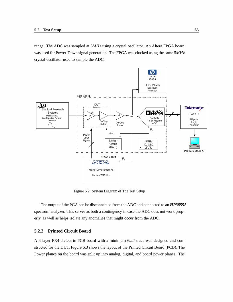
5.2. Test Setup 65
range. The ADC was sampled at 5MHz using a crystal oscillator. An Altera FPGA board
was used for Power-Down signal generation. The FPGA was clocked using the same 5MHz
crystal oscillator used to sample the ADC.
A
OnChipBuffer
Off ChipBuffer
x2AD9240
14 bit PipelineADC
Nios® Development Kit
Cyclone™ Edition
Divider
Circuit
(Div 8)
5MHz
XL OSC
DUTTest Chip
Test Board
Fchop
Fs
Fs
PowerDown
Signals
Model DS360Low Distortion Function
Generator
TLA 714
220 pointLogic
Analyzer
FPGA Board
Stanford Research
Systems
PC With MATLAB
3588A
10Hz - 150MHzSpectrumAnalyzer
Figure 5.2: System Diagram of The Test Setup
The output of the PGA can be disconnected from the ADC and connected to anHP3855A
spectrum analyzer. This serves as both a contingency in casethe ADC does not work prop-
erly, as well as helps isolate any anomalies that might occurfrom the ADC.
5.2.2 Printed Circuit Board
A 4 layer FR4 dielectric PCB board with a minimum 6mil trace was designed and con-
structed for the DUT. Figure 5.3 shows the layout of the Printed Circuit Board (PCB). The
Power planes on the board was split up into analog, digital, and board power planes. The

5.2. Test Setup 66
power supply voltages for the DUT, and other on-board IC’s were generated by low noise
LM1117 regulators. The common mode was generated by using a potentiometer as a resis-
tor divider. The desired voltage is then buffered through anLM7301 opamp connected in
unity gain configuration.
Figure 5.3: Printed Circuit Board Layout
5.2.3 IC Test Methodology
Due to limitations in the test setup, the DUT was tested underslightly different than the
intended operation. Figure 5.4 illustrates a representation of the intended operation (a),
which was also illustrated in chapter 3, and the testing method when the power-down modes
are used (b).

5.2. Test Setup 67
count =
5,000
N
N+M
POWERED
DOWN
POWERED
UP
PDN
count =
500POWERED
DOWN
POWERED
UP
PDN
One Sample One Sample
5,000
Samples
5,000
Samples
ton
= 1ms
ton
= 0.1ms
pd_bias=0
pd=0
(a)
(b)
Figure 5.4: Power-Down Cycle (a)intended operation, and (b)measured
Because the logic analyzer could only store 220 = 1048576 points, if we were to average
5000 sample points for every ON time (as shown in figure 5.4(a)), we would end up with
only 200 points to plot an FFT. As an alternative, only one point was sampled every ON
time (as shown in figure 5.4(b)). Moreover, in the power down by 1000 case (where the
input signal is 0.5Hz), the interface would be ON for 1ms, and OFF for 0.999s. That means
that we would take only one data point every second, which meant that we would have
to wait a million seconds for a million point FFT! In order to reduce the testing time, we
reduced the power down period by a factor of 10, while keepingthe ON/OFF duty cycle
the same. Moreover, as we go to lower input frequencies, the number of FFT points was
reduced, in order to reduce the data capture time.
For the “No-Power-Down” case (Fin = 0.5kHz) the signal was sampled at the full rate
of 5MHz (OSR = 5000), and the full million point FFT was taken withoutaveraging every
5000 samples.
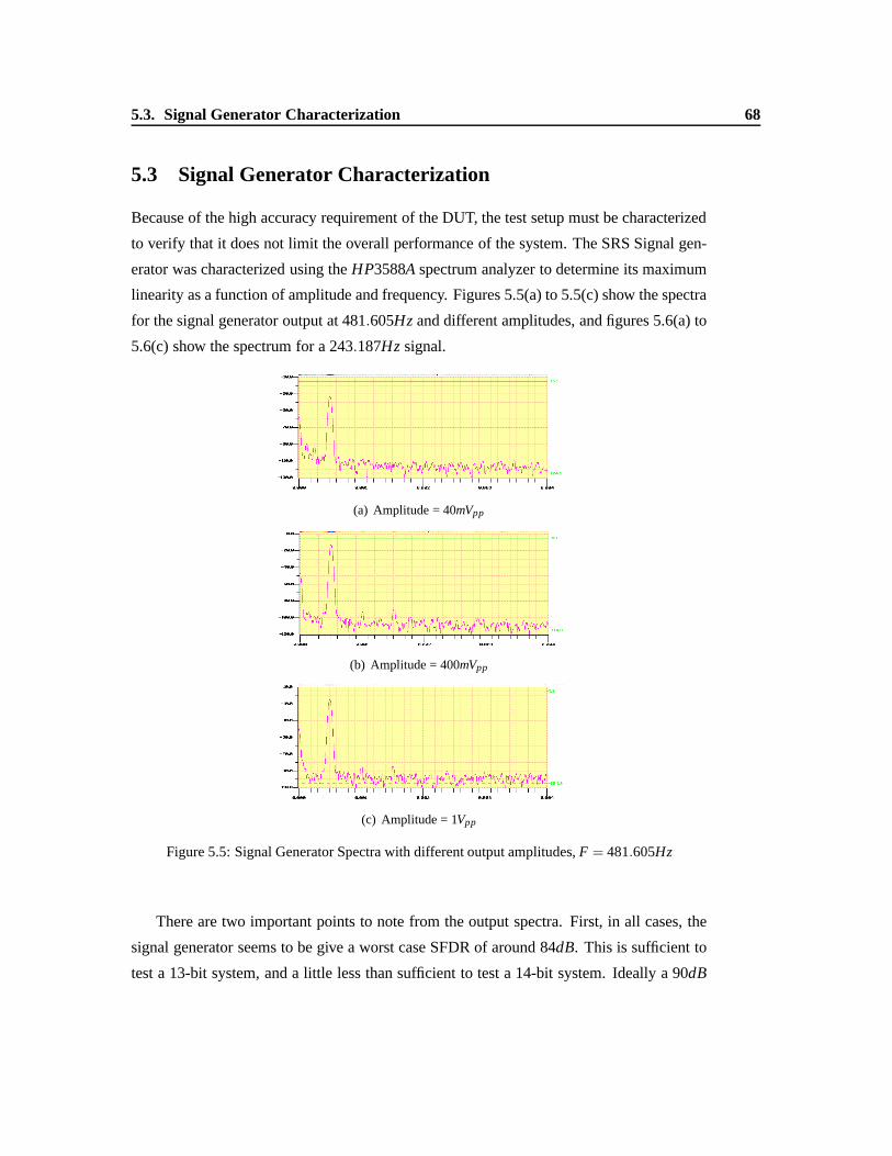
5.3. Signal Generator Characterization 68
5.3 Signal Generator Characterization
Because of the high accuracy requirement of the DUT, the testsetup must be characterized
to verify that it does not limit the overall performance of the system. The SRS Signal gen-
erator was characterized using theHP3588A spectrum analyzer to determine its maximum
linearity as a function of amplitude and frequency. Figures5.5(a) to 5.5(c) show the spectra
for the signal generator output at 481.605Hz and different amplitudes, and figures 5.6(a) to
5.6(c) show the spectrum for a 243.187Hz signal.
(a) Amplitude = 40mVpp
(b) Amplitude = 400mVpp
(c) Amplitude = 1Vpp
Figure 5.5: Signal Generator Spectra with different outputamplitudes,F = 481.605Hz
There are two important points to note from the output spectra. First, in all cases, the
signal generator seems to be give a worst case SFDR of around 84dB. This is sufficient to
test a 13-bit system, and a little less than sufficient to testa 14-bit system. Ideally a 90dB

5.4. ADC Characterization 69
(a) Amplitude = 40mVpp
(b) Amplitude = 400mVpp
(c) Amplitude = 1Vpp
Figure 5.6: Signal Generator Spectra with different outputamplitudes,F = 243.187Hz
dynamic range signal source would be sufficient to test a 14 bit system, to ensure that the
system is not limited by the signal source. Second, it is apparent that there is a 60Hz (and
its harmonics) component in the output signal. This will be ignored in any further analysis
of test results for the DUT, since the target application is battery powered and would not
suffer from AC supply noise.
5.4 ADC Characterization
As was mentioned in theTest Setup section, a 5MHz ADC was used on board to digitize the
output sine wave for analysis. The AD9240 was characterizedby applying the input from
the SRS signal generator directly into the ADC input throughSMA connectors at the input

5.4. ADC Characterization 70
of the ADC. The reference voltage of the ADC was measured to be1.5V (Vtop = 4.0V ,
Vtop = 1.0V , andVCM = 2.5V ). Figures 5.7 and 5.8 show the Spurious Free Dymanic
Range (SFDR) and the Total Harmonic Distortion (THD), respectively of the ADC.
60.00
62.00
64.00
66.00
68.00
70.00
72.00
74.00
76.00
78.00
80.00
0 500 1000 1500 2000 2500
Input Amplitude (mV)
SF
DR
(d
B) F = 481 Hz
F = 243 Hz
F = 48 Hz
F = 4.8 Hz
F = 0.48 Hz
Figure 5.7: SFDR Vs Input amplitude of the External ADC
60.00
62.00
64.00
66.00
68.00
70.00
72.00
74.00
76.00
0 500 1000 1500 2000 2500
Input Amplitude (mV)
TH
D7
(d
B) F = 481 Hz
F = 243 Hz
F = 48 Hz
F = 4.8 Hz
F = 0.48 Hz
Figure 5.8: THD7 Vs Input amplitude of the External ADC
Figure 5.9 shows some sample power spectral density plots ofthe ADC output with
different input amplitudes. From the PSD’s we can see that there are higher order spurs
that dominate over the third order harmonic. That may be attributed to the fact that the
ADC input was not buffered, or that the voltage references are not clean. Due to the lack of
testability in the external ADC, it was difficult to ascertain the cause of that dominant 5,6
and 7th order harmonics.
Figures 5.10 and 5.11 show the SFDR and THD plots of the ADC that only include up

5.5. IC Test Results 71
101
102
103
104
105
106
107
−200
−180
−160
−140
−120
−100
−80
−60
−40
−20
0PSD
Am
plitu
de(d
B)
Frequency [Hz]
60Hz120Hz
240Hz 2nd
3rd
(a) Input = 400mVpp
101
102
103
104
105
106
107
−200
−180
−160
−140
−120
−100
−80
−60
−40
−20
0PSD
Am
plitu
de(d
B)
Frequency [Hz]
60Hz120Hz
240Hz
2nd
3rd
(b) Input = 800mVpp
101
102
103
104
105
106
107
−200
−180
−160
−140
−120
−100
−80
−60
−40
−20
0PSD
Am
plitu
de(d
B)
Frequency [Hz]
120Hz
240Hz
2nd
3rd
(c) Input = 1000mVpp
101
102
103
104
105
106
107
−200
−180
−160
−140
−120
−100
−80
−60
−40
−20
0PSD
Am
plitu
de(d
B)
Frequency [Hz]
60Hz120Hz
240Hz
2nd
3rd
(d) Input = 2000mVpp
Figure 5.9: ADC Characterization Spectra,Fin = 481.605Hz
to the third order harmonic. The difference between the curves below and above clearly
indicate that in nearly 50% of the cases, the dominant harmonic was higher in frequency
than the third order harmonic.
5.5 IC Test Results
5.5.1 DC Bias Points
Because of the analog test mux (AMUX) that was designed, it was relatively easy to be
able to probe the DC bias voltages of the OPAMPs and compare them to the simulations.

5.5. IC Test Results 72
60.00
65.00
70.00
75.00
80.00
85.00
90.00
0 500 1000 1500 2000 2500
Input Amplitude (mV)
SF
DR
(d
B) F = 481 Hz
F = 243 Hz
F = 48 Hz
F = 4.8 Hz
F = 0.48 Hz
Figure 5.10: SFDR Vs Input amplitude of the External ADC
60.00
62.00
64.00
66.00
68.00
70.00
72.00
74.00
76.00
78.00
80.00
0 500 1000 1500 2000 2500
Input Amplitude (mV)
TH
D3
(d
B) F = 481 Hz
F = 243 Hz
F = 48 Hz
F = 4.8 Hz
F = 0.48 Hz
Figure 5.11: THD3 Vs Input amplitude of the External ADC
table 5.1 below shows the measured and simulated (over typical and slow corners) results
of DC bias points in the Amplifier OPAMPs as well as the buffer.Refer to figure 4.5 for
the bias voltage names.
Relative to the typical corner, all of the measured bias voltages were within 50mV from
the simulated values. This table shows that all current sources and cascode transistors are
well within the active region, with no transistors in triode.

5.5. IC Test Results 73
Table 5.1: DC Bias Points: Simulated and Measured
AMPLIFIER1 AMPLIFIER 2,3 BUFFERSimulated Measured Simulated Measured Simulated Measured[V] [V] [V] [V] [V] [V] [V] [V] [V](TT) (SS) (TT) (SS) (TT) (SS)
V DD 1.80 1.80 1.80 1.80 1.80 1.80 1.91 1.91 1.91V BP 1.22 1.17 1.17 1.22 1.17 1.17 1.36 1.31 1.31V BN 0.60 0.66 0.62 0.60 0.66 0.63 0.58 0.64 0.61V BP1 0.83 0.77 0.86 0.83 0.77 0.83 0.99 0.94 1.00V BN1 0.99 1.04 0.94 0.99 1.04 0.97 0.92 0.99 0.87V BPCASC 1.21 1.17 1.16 1.21 1.17 1.16 1.34 1.30 1.29V BNCASC 0.62 0.67 0.65 0.62 0.67 0.66 0.59 0.64 0.61
5.5.2 Spurious Free Dynamic Range (SFDR)
In this section we show the SFDR performance of the DUT. Having tested the performance
limits of the external ADC and the signal source, we are now able to see how well the DUT
performs, knowing that the overall system can be limited by the ADC performance. Figure
5.12 below shows the SFDR plot of the DUT. The input is swept from 40mVpp to 1.0Vpp at
an input frequency of 481.6Hz, while adjusting the gain setting so that the output is at least
400mVpp. The plot shows that the SFDR ranges from approximately 72dB to 97dB.
65.00
70.00
75.00
80.00
85.00
90.00
95.00
100.00
10 100 1000
Input Amplitude (mV)
SF
DR
(d
B)
Gain 10
Gain 4
Gain 2
Gain 1
Figure 5.12: SFDR Vs Input Amplitude with different Gain settings
Figures 5.13(a)to 5.13(h) show the power spectral densities of the system output. The
60Hz components and its harmonics were ignored in the SFDR calculation. The spurs past
the third harmonic were similar to the higher order spurs observed in the ADC output PSD.

5.5. IC Test Results 74
101
102
103
104
105
106
107
−200
−180
−160
−140
−120
−100
−80
−60
−40
−20
0PSD
Am
plitu
de(d
B)
Frequency [Hz]
60Hz120Hz
240Hz
360Hz
Modulated Offset and 1/F noise
(a) Input = 40mVpp, Gain = 10
101
102
103
104
105
106
107
−200
−180
−160
−140
−120
−100
−80
−60
−40
−20
0PSD
Am
plitu
de(d
B)
Frequency [Hz]
60Hz120Hz
240Hz
360Hz
Modulated Offset and 1/F noise
3rd
(b) Input = 100mVpp, Gain = 10
101
102
103
104
105
106
107
−200
−180
−160
−140
−120
−100
−80
−60
−40
−20
0PSD
Am
plitu
de(d
B)
Frequency [Hz]
60Hz120Hz
240Hz
360Hz
Modulated Offset and 1/F noise
2nd
3rd
(c) Input = 100mVpp, Gain = 4
101
102
103
104
105
106
107
−200
−180
−160
−140
−120
−100
−80
−60
−40
−20
0PSD
Am
plitu
de(d
B)
Frequency [Hz]
60Hz120Hz
240Hz
360Hz
Modulated Offset and 1/F noise
ADC Spurs
(d) Input = 200mVpp , Gain = 4
101
102
103
104
105
106
107
−200
−180
−160
−140
−120
−100
−80
−60
−40
−20
0PSD
Am
plitu
de(d
B)
Frequency [Hz]
60Hz120Hz
240Hz
360Hz
Modulated Offset and 1/F noise
ADC Spurs
2nd
3rd
(e) Input = 200mVpp, Gain = 2
101
102
103
104
105
106
107
−200
−180
−160
−140
−120
−100
−80
−60
−40
−20
0PSD
Am
plitu
de(d
B)
Frequency [Hz]
60Hz120Hz
240Hz
360Hz
Modulated Offset and 1/F noise
ADC Spurs
(f) Input = 400mVpp, Gain = 2
101
102
103
104
105
106
107
−200
−180
−160
−140
−120
−100
−80
−60
−40
−20
0PSD
Am
plitu
de(d
B)
Frequency [Hz]
60Hz120Hz
240Hz
360Hz
Modulated Offset and 1/F noise
ADC Spurs
(g) Input = 400mVpp, Gain = 1
101
102
103
104
105
106
107
−200
−180
−160
−140
−120
−100
−80
−60
−40
−20
0PSD
Am
plitu
de(d
B)
Frequency [Hz]
60Hz120Hz
240Hz
360Hz
Modulated Offset and 1/F noise
ADC Spurs
(h) Input = 1Vpp, Gain = 1
Figure 5.13: PSD plots of DUT output with different Input andGain settings atFin =481.6Hz
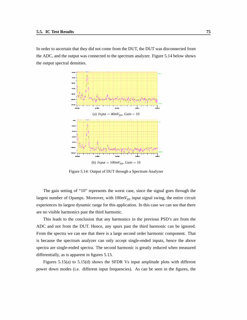
5.5. IC Test Results 75
In order to ascertain that they did not come from the DUT, the DUT was disconnected from
the ADC, and the output was connected to the spectrum analyzer. Figure 5.14 below shows
the output spectral densities.
(a) Input = 40mVpp, Gain = 10
(b) Input = 100mVpp, Gain = 10
Figure 5.14: Output of DUT through a Spectrum Analyzer
The gain setting of “10” represents the worst case, since thesignal goes through the
largest number of Opamps. Moreover, with 100mVpp input signal swing, the entire circuit
experiences its largest dynamic range for this application. In this case we can see that there
are no visible harmonics past the third harmonic.
This leads to the conclusion that any harmonics in the previous PSD’s are from the
ADC and not from the DUT. Hence, any spurs past the third harmonic can be ignored.
From the spectra we can see that there is a large second order harmonic component. That
is because the spectrum analyzer can only accept single-ended inputs, hence the above
spectra are single-ended spectra. The second harmonic is greatly reduced when measured
differentially, as is apparent in figures 5.13.
Figures 5.15(a) to 5.15(d) shows the SFDR Vs input amplitudeplots with different
power down modes (i.e. different input frequencies). As canbe seen in the figures, the

5.5. IC Test Results 76
65.00
70.00
75.00
80.00
85.00
90.00
95.00
10 100 1000
Input Amplitude (mV)
SF
DR
(d
B)
Gain 10
Gain 4
Gain 2
Gain 1
(a) Power Down by 2(Fin = 243.187Hz)
65.00
70.00
75.00
80.00
85.00
90.00
95.00
100.00
10 100 1000
Input Amplitude (mV)
SF
DR
(d
B)
Gain 10
Gain 4
Gain 2
Gain 1
(b) Power Down by 10(Fin = 48.6Hz)
65.00
70.00
75.00
80.00
85.00
90.00
95.00
100.00
10 100 1000
Input Amplitude (mV)
SF
DR
(d
B)
Gain 10
Gain 4
Gain 2
Gain 1
(c) Power Down by 100(Fin = 4.86Hz)
65.00
70.00
75.00
80.00
85.00
90.00
95.00
100.00
10 100 1000
Input Amplitude (mV)
SF
DR
(d
B)
Gain 10
Gain 4
Gain 2
Gain 1
(d) Power Down by 1000(Fin = 0.486Hz)
Figure 5.15: SFDR with different power down modes
results are consistent regardless of the power down mode. Moreover, for frequencies below
10Hz, the linearity of the signal source seems to deteriorate. Figures 5.16(a) to 5.16(d)
shows the PSD’s with the power down modes. Because there is nofilter to remove the
modulated offset and 1/F noise, they get aliased back in the visible band. In the power
down by 100 and 1000 cases, the 60Hz harmonics also bet aliased back.
5.5.3 Total Harmonic Distortion (THD)
Figure 5.17 shows the THD Vs input amplitudes with differentgain settings. Similar to the
SFDR, the THD was calculated by counting only up to the forth order harmonics. In the
previous section we have established that any higher order harmonics come from the ADC
as opposed to the DUT.
As with the SFDR case, it is worthwhile to see the effect of powering down on the
performance of the DUT. Figures 5.18(a) to 5.18(d) show the THD Vs input plots using
different power down modes. Once again, powering down causes no significant change in
performance.
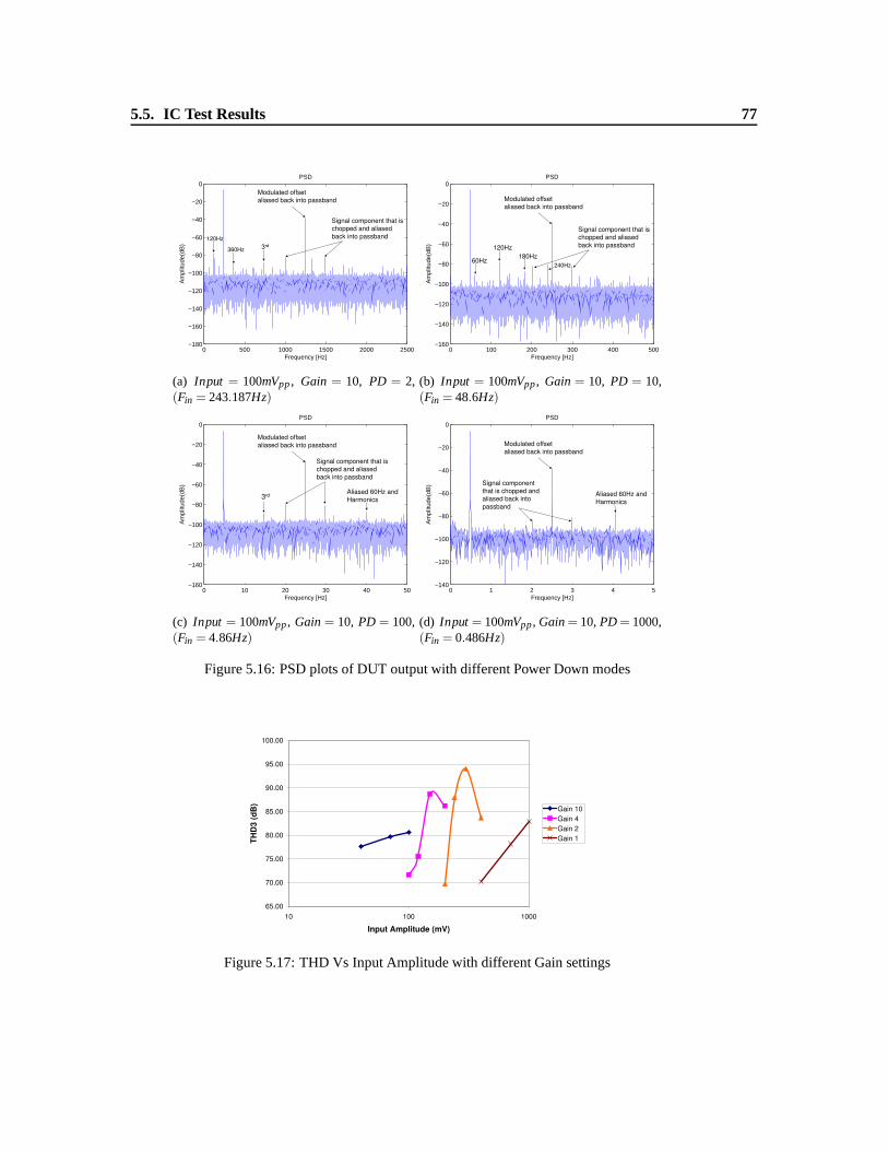
5.5. IC Test Results 77
0 500 1000 1500 2000 2500−180
−160
−140
−120
−100
−80
−60
−40
−20
0PSD
Am
plitu
de(d
B)
Frequency [Hz]
120Hz
Modulated offset aliased back into passband
Signal component that is chopped and aliased
back into passband
3rd360Hz
(a) Input = 100mVpp , Gain = 10, PD = 2,(Fin = 243.187Hz)
0 100 200 300 400 500−160
−140
−120
−100
−80
−60
−40
−20
0PSD
Am
plitu
de(d
B)
Frequency [Hz]
Modulated offset aliased back into passband
Signal component that is chopped and aliased
back into passband120Hz
240Hz
180Hz60Hz
(b) Input = 100mVpp, Gain = 10, PD = 10,(Fin = 48.6Hz)
0 10 20 30 40 50−160
−140
−120
−100
−80
−60
−40
−20
0PSD
Am
plitu
de(d
B)
Frequency [Hz]
Modulated offset aliased back into passband
Signal component that is chopped and aliased
back into passband
Aliased 60Hz and Harmonics3rd
(c) Input = 100mVpp, Gain = 10, PD = 100,(Fin = 4.86Hz)
0 1 2 3 4 5−140
−120
−100
−80
−60
−40
−20
0PSD
Am
plitu
de(d
B)
Frequency [Hz]
Signal component that is chopped and
aliased back into passband
Modulated offset aliased back into passband
Aliased 60Hz and Harmonics
(d) Input = 100mVpp, Gain = 10,PD = 1000,(Fin = 0.486Hz)
Figure 5.16: PSD plots of DUT output with different Power Down modes
65.00
70.00
75.00
80.00
85.00
90.00
95.00
100.00
10 100 1000
Input Amplitude (mV)
TH
D3
(d
B)
Gain 10
Gain 4
Gain 2
Gain 1
Figure 5.17: THD Vs Input Amplitude with different Gain settings

5.5. IC Test Results 78
65.00
70.00
75.00
80.00
85.00
90.00
95.00
100.00
10 100 1000
Input Amplitude (mV)
TH
D3
(d
B)
Gain 10
Gain 4
Gain 2
Gain 1
(a) Power Down by 2,(Fin = 243.187Hz)
65.00
70.00
75.00
80.00
85.00
90.00
95.00
100.00
10 100 1000
Input Amplitude (mV)
TH
D3
(d
B)
Gain 10
Gain 4
Gain 2
Gain 1
(b) Power Down by 10,(Fin = 48.6Hz)
65.00
70.00
75.00
80.00
85.00
90.00
95.00
100.00
10 100 1000
Input Amplitude (mV)
TH
D3
(d
B)
Gain 10
Gain 4
Gain 2
Gain 1
(c) Power Down by 100,(Fin = 4.86Hz)
65.00
70.00
75.00
80.00
85.00
90.00
95.00
100.00
10 100 1000
Input Amplitude (mV)
TH
D3
(d
B)
Gain 10
Gain 4
Gain 2
Gain 1
(d) Power Down by 1000,(Fin = 0.486Hz)
Figure 5.18: THD with different power down modes
5.5.4 Power Scaling
Now that we have established that the DUT is 13-bits linear onaverage, even under dif-
ferent power-down modes, it is time to see how well does the amplifier power scale. In
this section, we will measure how well the DUT power scales relative to amplitude and
bandwidth.
Amplitude Power Scaling
Figure 5.19 shows the PGA power consumption under differentgain settings. As can be
seen from the plot, the “Gain 4” setting (designed for 100mVpp input) consumes approxi-
mately 6 times less power than the “Gain 10” setting (designed for 40mVpp input). How-
ever, we notice that the “Gain 2” setting only consumes around 2.5 times less power than
the “Gain 4” setting. As explained in the previous section, this is because the total power
does not account for the opamp bias power consumption.
Figure 5.20 shows the amplitude power scaling plots with different power down modes.
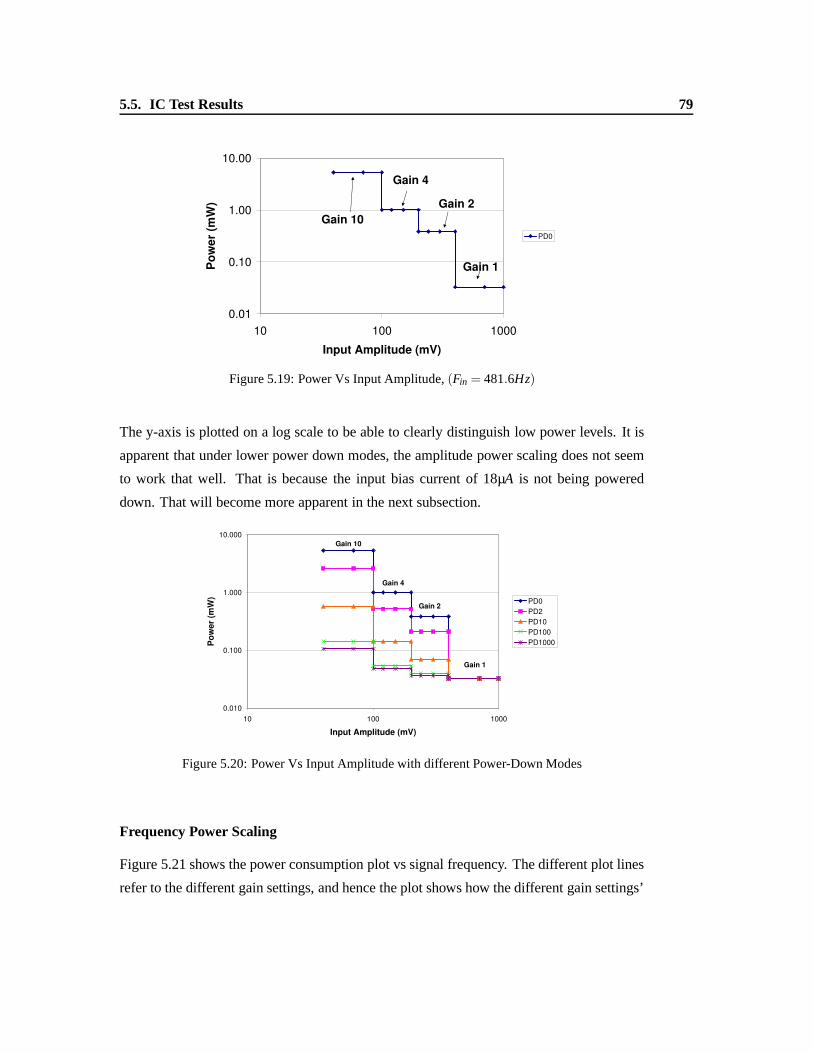
5.5. IC Test Results 79
0.01
0.10
1.00
10.00
10 100 1000
Input Amplitude (mV)
Po
wer
(mW
)
PD0
Gain 10
Gain 4
Gain 2
Gain 1
Figure 5.19: Power Vs Input Amplitude,(Fin = 481.6Hz)
The y-axis is plotted on a log scale to be able to clearly distinguish low power levels. It is
apparent that under lower power down modes, the amplitude power scaling does not seem
to work that well. That is because the input bias current of 18µA is not being powered
down. That will become more apparent in the next subsection.
0.010
0.100
1.000
10.000
10 100 1000
Input Amplitude (mV)
Po
we
r (m
W)
PD0
PD2
PD10
PD100
PD1000
Gain 10
Gain 4
Gain 2
Gain 1
Figure 5.20: Power Vs Input Amplitude with different Power-Down Modes
Frequency Power Scaling
Figure 5.21 shows the power consumption plot vs signal frequency. The different plot lines
refer to the different gain settings, and hence the plot shows how the different gain settings’

5.5. IC Test Results 80
power scales with frequency. The plot shows a very linear relationship between power
consumption and frequency, However, because the x-axis is plotted on a linear scale, it is
difficult to ascertain what is going on in the lower frequencyrange.
0.000
1.000
2.000
3.000
4.000
5.000
6.000
0.5 100.5 200.5 300.5 400.5
Input Frequency (Hz)
Po
wer
(mW
)
Gain 10
Gain 4
Gain 2
Gain 1
Figure 5.21: Frequency Power Scaling
Figure 5.22 shows the same plot, but with both x and y-axes on alog scale. From
this plot, we can see that frequency power scaling works welluntil the frequency is scaled
down to 50Hz after which it no longer scales linearly. Moreover, if we look at the 0.5Hz
power points, we can see as we indicated in the previous subsection that they do not power-
scale well with different gain settings. This can be seen easily, as the distance between
the different line-plots are not uniform, indicating a difference in power ratios between the
0.5Hz case and the 0.5kHz case.
In the previous subsection, we mentioned that the degradation in power-scalability can
be attributed to the fact that the input bias current is not powered down with the rest of the
circuit. Figure 5.23 shows the same frequency power-scaling plot after the constant input
bias current has been subtracted from the overall average current consumption.
In this case, the DUT’s power seems to scale better with frequency, although it still
does not scale perfectly linearly in the 0.5Hz case (equivalent to a power down mode of
1000). The “Gain 1” case, all amplifiers have been bypassed, and any power consumption
comes from leakages and the logic gain-selection blocks.

5.5. IC Test Results 81
0.000
0.001
0.010
0.100
1.000
10.000
0.1 1 10 100 1000
Input Frequency (Hz)
Po
wer
(mW
)
Gain 10
Gain 4
Gain 2
Gain 1
Figure 5.22: Frequency Power Scaling on a LOG scale
0.000
0.001
0.010
0.100
1.000
10.000
0.1 1 10 100 1000
Input Frequency (Hz)
Po
wer
(mW
)
Gain 10
Gain 4
Gain 2
Gain 1
Figure 5.23: Frequency Power Scaling after removing the Ibias
5.5.5 Effects of Chopping
It is important to find out how much impact on performance did chopping have on the DUT.
Figure 5.24 shows the output PSD (with and without a signal),for the “Gain 10” setting.
From the PSD’s, it is apparent that the inband noise reduced 4times as a result of chopping.
That translates into a 12dB difference in SNR, or 2−bits.
There was no accurate means to measure the residual offset ofthe amplifier, because
the test setup was not designed to measure it. This is not significantly important for this test
chip, as the goal in this case was to see the effect of choppingon 1/F noise, especially in
smaller technologies, where 1/F noise gets worse. We have shown here that we are capable

5.5. IC Test Results 82
101
102
103
104
105
106
107
−200
−180
−160
−140
−120
−100
−80
−60
−40
−20
0PSD
Am
plitu
de(d
B)
Frequency [Hz]
nochopchop
Modulated Offset and
1/F Noise
Vnoisenochop = 258.26 µVrms
Vnoisechop = 68.39 µVrms
(a) No signal
101
102
103
104
105
106
107
−200
−180
−160
−140
−120
−100
−80
−60
−40
−20
0PSD
Am
plitu
de(d
B)
Frequency [Hz]
nochopchop
Modulated Offset and
1/F Noise
SNRnochop = 60.3dB
SNRchop = 72.0dB
(b) With signal (40mV )
Figure 5.24: Effect of Chopping with and without signal,(Fin = 481.6Hz)

5.6. Summary 83
of achieving at least 12-bits noise level with relative to low signal amplitudes (40mVpp)
in 0.18µm CMOS technology. From the plots we can also see that the 1/F noise corner
frequency is approximately 50kHz.
5.6 Summary
Table 5.2 shows a comparison between simulated and measuredinterface power consump-
tion. As was mentioned in chapter 4, due to long simulation times, the power down modes
were not simulated, and so an accurate comparison can only bemade in the no power down
mode case (500Hz).
Table 5.2: Simulated Vs Measured Power Consumption
Input Amplitude Input Bandwidth Gain Simulated Power Measured Power(mVpp) Hz Setting Consumption (mW ) Consumption (mW )
40 500 10 5.278 5.296101 500 4 0.984 0.974201 500 2 0.349 0.353401 500 1 0.001 0.00140 50 10 N/A 0.545101 50 4 N/A 0.112201 50 2 N/A 0.038401 50 1 N/A 0.00140 5 10 N/A 0.112101 5 4 N/A 0.022201 5 2 N/A 0.007401 5 1 N/A 0.00140 0.5 10 N/A 0.074101 0.5 4 N/A 0.015201 0.5 2 N/A 0.004401 0.5 1 N/A 0.001
Tables 5.3 - 5.5 show the results summary for the DUT for different input voltage ranges
and gain settings. Overall, the test results show that a sensor interfacing PGA with 13-bit
linearity can be designed to be power-scalable in both frequency and amplitude.

5.6. Summary 84
Table 5.3: Results Summary for Input = 40mVpp - 100mVpp
Technology 0.18µm CMOSPower Supply 1.8V
ADC Sampling Freq. 5.0MHzSignal Bandwidth Range 0−0.5Hz(min), 0−0.5kHz(max)
Chopping Frequency 625.0kHzGain Settings 20dB
SFDR 72dB(min) 95dB(max)THD 70dB(min) 90dB(max)
Input Referred Noise 170.0nV /√
HzPower Consumption Range 74.0µW −5.30mW
PGA Area 0.617mm2
Table 5.4: Results Summary for Input = 100mVpp - 200mVpp
Technology 0.18µm CMOSPower Supply 1.8V
ADC Sampling Freq. 5.0MHzSignal Bandwidth Range 0−0.5Hz(min), 0−0.5kHz(max)
Chopping Frequency 625.0kHzGain Settings 12dBSFDR (Mean) 72dB(min) 95dB(max)THD (Mean) 70dB(min) 90dB(max)
Input Referred Noise 160.0nV /√
HzPower Consumption Range 15.0µW −0.974mW
PGA Area 0.617mm2
Table 5.5: Results Summary for Input = 200mVpp - 400mVpp
Technology 0.18µm CMOSPower Supply 1.8V
ADC Sampling Freq. 5.0MHzSignal Bandwidth Range 0−0.5Hz(min), 0−0.5kHz(max)
Chopping Frequency 625.0kHzGain Settings 6dBSFDR (Mean) 72dB(min) 95dB(max)THD (Mean) 70dB(min) 90dB(max)
Input Referred Noise 220.0nV /√
HzPower Consumption Range 4.0µW −0.35mW
PGA Area 0.617mm2

Chapter 6
Conclusion
I N this dissertation, a technique to improve power scaling efficiency of automotive
MEMS pressure sensor interfaces is presented. Power scaling with respect to ampli-
tude is achieved by cascading gain stages through an input gain-select mux, which scales
better than previous approaches which utilize either a cascaded gain stage with output gain
select, or varying the input and/or feedback impedances in anegative feedback configu-
ration. Power scaling with respect to input bandwidth of thesensor is achieved through
periodic power-down of the interface. A prototype of the interface was fabricated in 1.8V ,
0.18µm CMOS process. Its power consumption scales between 4µW − 5.33mW , while
maintaining a Spurious Free Dynamic Range (SFDR) range of approximately 72−92dB,
a Total Harmonic Distortion (THD) range of 70− 90dB, and an input referred noise of
170.0nV /√
Hz.
6.1 Future Work
As mentioned in the introduction, this work is part of a larger integrated system of MEMS
pressure sensors. This work presents a solution to a key challenge in meeting the system
expectations. Future work in this field would include:
• One key challenge with this project is that, while the analog power consumption
scales down with respect to both frequency, and amplitude, the digital power con-
sumption remains virtually constant, and large compared tothe scaled analog power.
Therefore, the Power Down FPGA was implemented off-chip. Low power digital
85
6.1. Future Work 86
techniques can be utilized to implement an On-chip FPGA, while maintaining the
overall power efficiency of the system.
• Integrating a low-power incremental ADC to follow the PGA interface stage. This
would provide a complete integrated solution for MEMS pressure sensors or any
other resistive-based pressure sensor.
• While this project deals with pressure sensors, the next step would be to implement
similar power-scalable topologies with different kinds ofsensors that may be capac-
itive, inductive, mechanical, or otherwise.
This work provides lots of promise in the field of sensor electronics. By reducing
cost pressures of producing customized electronics for each sensor application, the sensor
industry can look forward to having power efficient, and economical solution to a growing
market demand.

Appendix A
Output Noise of a Cascaded Amplifier with
Input Gain Select
Figure A.1 shows the noise model of the cascaded gain amplifier with a last stage active
RC amplifier. The resistor values are the same as the ones shown in figure 3.17 in chapter
3, which means
R1 = R
R2 = 2.5R
R3 = 6R
R4 = 12R
R5 = 24R
R6 = 48R
(A.1)
In order to analyze the worst case output noise of this system(Gain setting = 10), we
will use superposition to calculated the noise transfer function of each of the noise sources:
Vout
Vn6=
11+ R6Cs
(A.2)
Vout
Vn5= −
R6
R5
11+ R6Cs
(A.3)
Vout
Vn4= −
R6
R5
11+ R6Cs
(A.4)
87

Output Noise of a Cascaded Amplifier with Input Gain Select 88
+
-
R1
R2
+
-
R3
R4
+
-
R6
R5
C
Vout
Vin
Vn6
*V
n5
*
Vn4
*V
n3
*
Vn2
*V
n1
*
Figure A.1: Noise Model of Cascaded Gain Stage with Final Active RC Stage
Vout
Vn3=
R4
R3·
R6
R5
11+ R6Cs
(A.5)
Vout
Vn3=
R4
R3·
R6
R5
11+ R6Cs
(A.6)
Vout
Vn1= −
R2
R1·
R4
R3·
R6
R5
11+ R6Cs
(A.7)
(A.8)
Using those transfer functions to calculate the noise yields:
V 2out,n = 4KT R6
14R6C
+4KTR5
(
R6
R5
)2 14R6C
+4KT R4
(
R6
R5
)2 14R6C
+4KT R3
(
R4R6
R3R5
)2 14R6C
+4KTR2
(
R4R6
R3R5
)2 14R6C
+4KT R1
(
R2R4R6
R1R3R5
)2 14R6C
(A.9)
Which is dependant on the ration of the resistors. Substituting all the resistor values in
equation A.1 into equation A.9 yields
V 2out,n ≈
10KTC
(A.10)

References
[1] M. Metz, “Trends in automotive sensors,” BOSCH Researchand Technology Center,Tech. Rep., 2005.
[2] K.-F. Reinhart and M. Illing,Sensors for Automotive Technology. Wiley-VCH, 2003,ch. 2, pp. 5–21.
[3] G. Lammel, S. Armbruster, C. Schelling, and H. Benzel, “Next generation pressuresensors in surface micromachining technology,” BOSCH Research and TechnologyCenter, Tech. Rep., 2005.
[4] C. Lang and J. Vanderhaegen, “Kickoff meeting: ScalableADC,” Bosch RTC, Tech.Rep., 2006.
[5] I. Yokomori and Y. Suzuki,Sensors for Automotive Technology. Wiley-VCH, 2003,ch. 7, pp. 314–342.
[6] R. Henn, T. Honma, and S. Finkbeiner,Sensors for Automotive Technology. Wiley-VCH, 2003, ch. 5, pp. 123–158.
[7] R. Johnson and R. Johnson, “High temperature silicon-on-insulator pressure sensortechnology,” inProc. Third European Conference on High Temperature ElectronicsHITEN 99, 1999, pp. 45–48.
[8] R. Singh, L. L. Ngo, H. S. Seng, and F. Mok, “A silicon piezoresistive pressure sen-sor,” in Proc. First IEEE International Workshop on Electronic Design, Test and Ap-plications, 29–31 Jan. 2002, pp. 181–184.
[9] S. Ekelof and S. Ekelof, “The genesis of the wheatstone bridge,” Engineering Scienceand Education Journal, vol. 10, no. 1, pp. 37–40, 2001.
[10] D. A. Johns and K. Martin,Analog Integrated Circuit Design, C. Robey, Ed. JohnWiley & Sons, Inc., 1997.
[11] B. Rezavi,Design of Analog CMOS integrated Circuits. McGraw-Hill InternationalEdition, 2001.
89

References 90
[12] C. Enz and G. Temes, “Circuit techniques for reducing the effects of op-amp imper-fections: autozeroing, correlated double sampling, and chopper stabilization,”,Pro-ceedings of IEEE, vol. 84, no. 11, pp. 1584–1614, Nov. 1996.
[13] J. H. Anton Bakker, “High-accuracy CMOS smart temperature sensors,” Ph.D. dis-sertation, Delft University of Technology, 2000.
[14] A. Bakker and J. Huijsing, “A CMOS chopper opamp with integrated low-pass filter,”in Proc. 23rd European Solid-State Circuits Conference ESSCIRC ’97, 16–18 Sept.1997, pp. 200–203.
[15] A. Bakker and J. Huijsing, “Offset reduction in current-mode microsystems,” inProc.IEEE International Symposium on Circuits and Systems ISCAS ’96., ’Connecting theWorld’, vol. 4, 12–15 May 1996, pp. 344–347.
[16] D. McCartney, A. Sherry, J. O’Dowd, and P. Hickey, “A low-noise low-drift trans-ducer ADC,”IEEE Journal of Solid State Circuits, vol. 32, no. 7, pp. 959–967, 1997.
[17] A. Bakker, K. Thiele, and J. Huijsing, “A CMOS nested-chopper instrumentationamplifier with 100-nV offset,”IEEE Journal of Solid State Circuits, vol. 35, no. 12,pp. 1877–1883, Dec. 2000.
[18] C. Menolfi and Q. Huang, “A low-noise CMOS instrumentation amplifier for thermo-electric infrared detectors,”IEEE Journal of Solid State Circuits, vol. 32, no. 7, pp.968–976, July 1997.
[19] J. F. Witte, J. F. Witte, K. A. Makinwa, and J. H. Huijsing, “A CMOS chopper offset-stabilized opamp,” inProc. 32nd European Solid-State Circuits Conference ESSCIRC2006, K. A. Makinwa, Ed., 2006, pp. 360–363.
[20] M. Sanduleanu, A. Van Tuijl, R. Wassenaar, M. Lammers, and H. Wallinga, “A lownoise, low residual offset, chopped amplifier for mixed level applications,” inProc.IEEE International Conference on Electronics, Circuits and Systems, vol. 2, 7–10Sept. 1998, pp. 333–336.
[21] Y. Christoforou, “A chopper-based CMOS current sense instrumentation amplifier,”in Proc. 19th IEEE IMTC/2002 Instrumentation and Measurement Technology Con-ference, vol. 1, 21–23 May 2002, pp. 271–273.
[22] R. Schreier and G. Temes,Understanding Delta-Sigma Data Converters, S. Kar-talopoulos, M. Akay, J. Anderson, R. Baker, and J. E. Brewer,Eds. John Wiley& Sons, Inc., 2005.
[23] J. Robert and P. Deval, “A second-order high-resolution incremental A/D converterwith offset and charge injection compensation,”IEEE Journal of Solid State Circuits,vol. 23, no. 3, pp. 736–741, June 1988.
References 91
[24] J. Markus, J. Silva, and G. Temes, “Theory and applications of incremental∆−Σ con-verters,”IEEE Transactions on Circuits and Systems Part 1: Regular Papers, vol. 51,no. 4, pp. 678–690, April 2004.
[25] T. Caldwell and D. Johns, “An incremental data converter with an oversampling ratioof 3,” in Proc. Ph Research in Microelectronics and Electronics 2006 D, 12–15 June2006, pp. 125–128.
[26] B. Woo, “Digitally programmable gain amplifiers with arbitary range of integer val-ues,”Proceedings of the IEEE, vol. 68, no. 7, pp. 934–936, July 1980.
[27] S. C. D. Roy, “Digitally programmable gain amplifiers,”IEEE Transactions on In-strumentation and Measurement, vol. 33, no. 4, pp. 329–332, Dec. 1984.
[28] G. Xu, G. Xu, and H. Bilhan, “A programmable gain amplifier buffer design for videoapplications,” inProc. International Symposium on Circuits and Systems ISCAS ’04,H. Bilhan, Ed., vol. 1, 2004, pp. I–557–60 Vol.1.
[29] F. Gebara, S. Martin, E. Marsman, K. Kraver, and R. Brown, “900mV programmablegain amplifier for cochlear implants,” inProc. IEEE International Workshop onBiomedical Circuits and Systems, 1–3 Dec. 2004, pp. S1/3/INV–S1/3/1–4.
[30] G. O’Donoghue, M. Mallinson, and P. Holloway, “A novel programmable gain ampli-fier,” in Proc. Third Annual IEEE ASIC Seminar and Exhibit, 17–21 Sept. 1990, pp.P8/6.1–P8/6.4.
[31] M. Sanz, M. Sanz, S. Celma, and B. Calvo, “Approach to high-linear programmablegain amplifiers,” inProc. 47th Midwest Symposium on Circuits and Systems MWSCAS’04, S. Celma, Ed., vol. 1, 2004, pp. I–157–60 vol.1.
[32] S. Spiridon and F. Op’t Eynde, “Low power CMOS fully differential variable-gainamplifier,” in Proc. International Semiconductor Conference CAS 2005, vol. 2, 3–5Oct. 2005, pp. 383–386.
[33] P. Furth and H. Om’mani, “A 500-nW floating-gate amplifier with programmablegain,” in Proc. Midwest Symposium on Circuits and Systems, 9–12 Aug. 1998, pp.134–137.
[34] C. Motchenbacher and J. Connelly,Low-Noise Electronic System Design,A. Gasiewski, E. Kennedy, and E. Chenette, Eds. John Wiley & Sons, Inc., 1993.
[35] I. Ahmed, “A power scaleable and low power pipeline ADC using power resettableopamps,” Master’s thesis, University of Toronto, 2004.
[36] I. Ahmed and D. Johns, “A 50 MS/s (35 mW) to 1 kS/s (15µ W) power scaleable10b pipelined ADC with minimal bias current variation,” inProc. Digest of Technical

References 92
Papers Solid-State Circuits Conference ISSCC. 2005 IEEE International, 6–10 Feb.2005, pp. 280–598.
[37] M. Dessouky and A. Kaiser, “Very low-voltage digital-audio ∆−Σ; modulator with88-dB dynamic range using local switch bootstrapping,”IEEE Journal of Solid StateCircuits, vol. 36, no. 3, pp. 349–355, March 2001.
[38] M. Dessouky and A. Kaiser, “Very low-voltage fully differential amplifier forswitched-capacitor applications,” inProc. ISCAS 2000 Geneva Circuits and SystemsThe 2000 IEEE International Symposium on, vol. 5, 28–31 May 2000, pp. 441–444.
[39] A. Sedra and K. Smith,Microelectronic Circuits, Fifth Edition, A. Sedra, Ed. OxfordUniversity Press, 2004.