Embed Size (px)
Citation preview

CVD growth of (001) and (111) 3C-SiC Epilayers and Their Interface
Reactivity with Praseodymium Oxide Dielectric Layers
Von der Fakultät für Mathematik, Naturwissenschaften und Informatik
der Brandenburgischen Technischen Universität Cottbus
zur Erlangung des akademischen Grades
Doktor der Naturwissenschaften
(Dr. rer. nat.)
genehmigte Dissertation
vorgelegte von
Master of Science in Physics Master of Technology in Materials Science & Engineering
Rakesh Sohal
geboren am 20. Mai 1974 in Rohtak, Indien
Gutachter:
Prof. Dr. rer. nat. habil Dieter Schmeißer
PD Dr. rer. nat. habil Christian Pettenkofer
PD Dr. rer. nat. habil Dietmar Siche
Tag der mündlichen Prüfung: 24. Juli 2006

ii
Dedicated
To my beloved parents
Smt. Santro Devi and Shri Balwan Singh
“You have a right to perform your prescribed duty, but you are not entitled to the
fruits of action. Never consider yourself the cause of the results of your activities, and
never be attached to not doing your duty.” – Bhagwat Gita

iii
Acknowledgements
I would like to express my sincere gratitude to Prof. Dr. Dieter Schmeißer for his dedicated
guidance throughout the course of this thesis work. His expertise and friendly advice were essential
to the successful completion of this Ph. D. thesis at BTU Cottbus. Special thanks are given to Dr.
Chacko Jacob at Materials Science Centre, IIT Kharagpur India for valuable discussions and
suggestions before and during this work.
I would also like to thank the committee members, Dr. Pettenkofer and Dr. Siche for their
acceptance to evaluate this manuscript.
I would like to appreciate the support of all my colleagues who have made the completion of
this work possible: Karsten Henkel, Dr. Patrick Hoffman for their technical assistance and scientific
discussions, Dr. Massimo Tallarida, Dr. Klaus Müller and Dr. Andre Goryachko for their scientific
discussions, Guido Beukert for his technical assistance. I would also like to thank Ioanna Paloumpa,
Carola Schwiertz, Karsten Henkel, Anja Schieferdecker, Guido Beukert and Patrick Hoffman,
Mohamed Torche, Olaf Seifarth, Suzan Winzer, Matthias Bergholz, Darmawan Bhoga and
Dipankar Mandal for their friendly assistance and environment making my stay in Cottbus easy,
joyful and learning experience. I would like to acknowledge the support from IKZ for providing
silicon wafers and their valuable discussions. I also acknowledge the support of Dr. Peter Zaumzeil
and Dr. Anil Mane at IHP Frankfurt (Oder). I specially thank Dr. Thomas Schröder, who availed for
this opportunity of research for doctoral degree.
I appreciate the support of all of my family members, parents, sister Sunita and brother
Montu. Their understanding and encouragement have sustained me through many difficult and
challenging moments. I also like to acknowledge the support and inspiration from my friends,
Nizamuddin, Amit, Prof. P. K. Chattopadhyay, and many others, who have accompanied me along
the journey.
Finally, I greatly appreciate the financial support from the DFG under the project DFG-SCHM
745/9-2 and also acknowledge the chance offered by Prof Dr. Dieter Schmeißer.

iv
CVD growth of (001) and (111) 3C-SiC Epilayers and Their Interface Reactivity with
Praseodymium Oxide Dielectric Layers
Rakesh Sohal
Brandenburgische Technische Universität Cottbus, 2006
Zusammenfassung
Im Rahmen dieser Arbeit wird das Wachstum und die Charakterisierung von 3C-SiC Filmen,
deren Oxidation, sowie das darauf präparierte Pr-Silikat und die AlON abgeleitete Grenzfläche
untersucht. Dünne 3C-SiC Filme wurden auf Si(001) und Si(111) Oberflächen mit Hilfe von
Chemical Vapor Deposition Verfahren hergestellt. Vor dem eigentlichen SiC-Wachstum wurde eine
SiC Zwischenschicht präpariert. Durch diese Buffer-Schicht wurde das epitaktische Wachstum von
3C-SiC auf Si(111) und Si(001) erst ermöglicht. Als optimale Präparationstemperaturen für 3C-SiC
auf Si(111) und Si(001) konnten 1100°C und 1150°C gefunden werden.
Im Verlaufe der Oxidation hat sich ein langsamer Stufenprozess mit moderaten Temperaturen
als hilfreich erwiesen, um die Graphitisierung an der SiO2/SiC Grenzfläche zu minimieren.
Sauberes, graphitfreies SiO2 konnte somit auf 3C-SiC mit Hilfe von Si-Evaporation und Heizen im
Vakuum hergestellt werden. Für mögliche Anwendung von Pr2O3 auf Siliziumkarbid als high-k
Dielektrikum wurden weiterhin Pr-Silikate und AlON untersucht. Praseodymium-Silikat konnte
erfolgreich auf der SiO2 Oberfläche abgeschieden werden und gleichzeitig die Graphitisierung
verhindert werden. Im Vergleich hierzu konnten sehr stabile Grenzflächen mit AlON hergestellt
werden. Diese Grenzflächen bestehen hauptsächlich aus AlN mit Anteilen von Pr-Al Komplexen.
Diese Schichten können als Reaktionsbarrieren zwischen Pr2O3 und SiC dienen und gleichzeitig
den Band-Offset vergrößern.

v
CVD growth of (001) and (111) 3C-SiC Epilayers and Their Interface Reactivity with
Praseodymium Oxide Dielectric Layers
Rakesh Sohal
Brandenburgische Technische Universität Cottbus, 2006
Abstract
In this work, growth and characterisation of 3C-SiC thin films, investigation of oxidation of
thus prepared layers and Pr-silicate and AlON based interface with SiC have been studied.
Chemical vapor deposition of 3C-SiC thin films on Si(001) and Si(111) substrates has been
investigated. Prior to the actual SiC growth, preparation of initial buffer layers of SiC was done.
Using such a buffer layer, epitaxial growth of 3C-SiC has been achieved on Si(111) and Si(001)
substrates. The temperature of 1100°C and 1150°C has been determined to be the optimal
temperature for 3C-SiC growth on Si (111) and Si(001) substrates respectively.
The oxidation studies on SiC revealed that a slow oxidation process at moderate temperatures
in steps was useful in reducing and suppressing the g-C at the SiO2/SiC interface. Clean, graphite-
free SiO2 has been successfully grown on 3C-SiC by silicon evaporation and UHV anneal. For the
application of high-k Pr2O3 on silicon carbide, plausible interlayer, Pr-Silicate and AlON, have been
investigated. Praseodymium silicate has been prepared successfully completely consuming the SiO2
and simultaneously suppressing the graphitic carbon formation. A comparatively more stable
interlayer using AlON has been achieved. This interlayer mainly consists of stable phases of AlN
along with some amount of Pr-aluminates and CN. Such layers act as a reaction barrier between
Pr2O3 and SiC, and simultaneously provide higher band offsets.

vi
Contents
Acknowledgements . . . . . . . . . . . . . . . . . . . . . . . . . . . . . . . . . . . . . . . . . . . . . . . . . . . . . . . .
Abstract (German) . . . . . . . . . . . . . . . . . . . . . . . . . . . . . . . . . . . . . . . . . . . . . . . . . . . . . . . .
Abstract (English) . . . . . . . . . . . . . . . . . . . . . . . . . . . . . . . . . . . . . . . . . . . . . . . . . . . . . . . . .
List of abbreviations & Symbols . . . . . . . . . . . . . . . . . . . . . . . . . . . . . . . . . . . . . . . . . . . . . 1. Introduction . . . . . . . . . . . . . . . . . . . . . . . . . . . . . . . . . . . . . . . . . . . . . . . . . . . . . . . . . . . . .
. 2. Silicon Carbide and Dielectrics: Background . . . . . . . . . . . . . . . . . . . . . . . . . . . . . . . . . .
. 2.1. Polytypism in silicon carbide . . . . . . . . . . . . . . . . . . . . . . . . . . . . . . . . . . . . . . . . . . . . .
. 2.2. SiC: Physical Properties . . . . . . . . . . . . . . . . . . . . . . . . . . . . . . . . . . . . . . . . . . . . . . . . .
. 2.3. SiC: Electronic Band Structures . . . . . . . . . . . . . . . . . . . . . . . . . . . . . . . . . . . . . . . . . . .
. 2.4. Figures of Merits . . . . . . . . . . . . . . . . . . . . . . . . . . . . . . . . . . . . . . . . . . . . . . . . . . . . . .
. 2.5. 3C-SiC: Surfaces . . . . . . . . . . . . . . . . . . . . . . . . . . . . . . . . . . . . . . . . . . . . . . . . . . . . . .
. 2.6. Silicon Carbide Oxidation . . . . . . . . . . . . . . . . . . . . . . . . . . . . . . . . . . . . . . . . . . . . . . .
. 2.7. Alternate Dielectrics on SiC . . . . . . . . . . . . . . . . . . . . . . . . . . . . . . . . . . . . . . . . . . . . . .
. 2.8. References . . . . . . . . . . . . . . . . . . . . . . . . . . . . . . . . . . . . . . . . . . . . . . . . . . . . . . . . . . .
. 3. Bulk and thin film growth . . . . . . . . . . . . . . . . . . . . . . . . . . . . . . . . . . . . . . . . . . . . . . . . . .
. 3.1. Bulk growth . . . . . . . . . . . . . . . . . . . . . . . . . . . . . . . . . . . . . . . . . . . . . . . . . . . . . . . . . .
. 3.1.1. Acheson Process . . . . . . . . . . . . . . . . . . . . . . . . . . . . . . . . . . . . . . . . . . . . . . . . .
. .
3.1.2. Lely Process . . . . . . . . . . . . . . . . . . . . . . . . . . . . . . . . . . . . . . . . . . . . . . . . . . . . .
.
3.1.3. Modified Lely Process . . . . . . . . . . . . . . . . . . . . . . . . . . . . . . . . . . . . . . . . . . . . .
.
3.1.4. Bulk growth - Control Parameters . . . . . . . . . . . . . . . . . . . . . . . . . . . . . . . . . . . .
.
3.2. Thin film growth . . . . . . . . . . . . . . . . . . . . . . . . . . . . . . . . . . . . . . . . . . . . . . . . . . . . . . . .
3.2.1. Molecular Beam Epitaxy . . . . . . . . . . . . . . . . . . . . . . . . . . . . . . . . . . . . . . . . . . .
.
3.2.2. Chemical Vapour Deposition . . . . . . . . . . . . . . . . . . . . . . . . . . . . . . . . . . . . . . .
. 3.2.2.1. SiC: Homoepitaxy . . . . . . . . . . . . . . . . . . . . . . . . . . . . . . . . . . . . . . . . . . . . . . . .
iii iv v ix 1 9 9 11 14 15 16 17 19 20 27 27 28 28 28 29 30 31 31 35

vii
. 3.2.2.2. SiC: Heteroepitaxy . . . . . . . . . . . . . . . . . . . . . . . . . . . . . . . . . . . . . . . . . . . . . . .
. 3.3. References . . . . . . . . . . . . . . . . . . . . . . . . . . . . . . . . . . . . . . . . . . . . . . . . . . . . . . . . . . . .
. 4. Experimental . . . . . . . . . . . . . . . . . . . . . . . . . . . . . . . . . . . . . . . . . . . . . . . . . . . . . . . . . . . . .
. 4.1. CVD Growth of 3C-SiC . . . . . . . . . . . . . . . . . . . . . . . . . . . . . . . . . . . . . . . . . . . . . . . . .
. 4.1.1. CVD Reactor: General Information . . . . . . . . . . . . . . . . . . . . . . . . . . . . . . . . . . .
.
4.1.2. Substrate cleaning prior to CVD growth . . . . . . . . . . . . . . . . . . . . . . . . . . . . . . .
.
4.1.3. Chemical vopor deposition process . . . . . . . . . . . . . . . . . . . . . . . . . . . . . . . . . . .
.
4.2. Oxidation of 3C-SiC . . . . . . . . . . . . . . . . . . . . . . . . . . . . . . . . . . . . . . . . . . . . . . . . . . . . .
4.3. Praseodymium Silicate on SiC . . . . . . . . . . . . . . . . . . . . . . . . . . . . . . . . . . . . . . . . . . . . .
4.4. Aluminium Oxinitride as Interlayer . . . . . . . . . . . . . . . . . . . . . . . . . . . . . . . . . . . . . . . . .
4.5. Characterisation techniques . . . . . . . . . . . . . . . . . . . . . . . . . . . . . . . . . . . . . . . . . . . . . . .
4.5.1. X-rays Photoelectron Spectroscopy . . . . . . . . . . . . . . . . . . . . . . . . . . . . . . . . . . .
. .
4.5.2. Fourier Transformed Infrared Spectroscopy . . . . . . . . . . . . . . . . . . . . . . . . . . . .
.
4.5.3. X-rays Diffraction . . . . . . . . . . . . . . . . . . . . . . . . . . . . . . . . . . . . . . . . . . . . . . . . .
.
4.5.4. Scanning Electron Microscopy . . . . . . . . . . . . . . . . . . . . . . . . . . . . . . . . . . . . . . .
.
4.5.5. Low Energy Electron Diffraction . . . . . . . . . . . . . . . . . . . . . . . . . . . . . . . . . . . .
.
4.5.6. Electron Energy Loss Spectroscopy . . . . . . . . . . . . . . . . . . . . . . . . . . . . . . . . . . .
.
5. Results and Discussion . . . . . . . . . . . . . . . . . . . . . . . . . . . . . . . . . . . . . . . . . . . . . . . . . . . . . . 5.1. CVD Growth of 3C-SiC . . . . . . . . . . . . . . . . . . . . . . . . . . . . . . . . . . . . . . . . . . . . . . . . .
. 5.1.1. Carbonisation: Buffer layer formation . . . . . . . . . . . . . . . . . . . . . . . . . . . . . . . .
.
5.1.2. Cubic Silicon Carbide Growth . . . . . . . . . . . . . . . . . . . . . . . . . . . . . . . . . . . . . . .
.
5.1.3. Discussion . . . . . . . . . . . . . . . . . . . . . . . . . . . . . . . . . . . . . . . . . . . . . . . . . . . . . . .
.
5.2. SiO2 on 3C-SiC . . . . . . . . . . . . . . . . . . . . . . . . . . . . . . . . . . . . . . . . . . . . . . . . . . . . . . . . .
5.3. Praseodymium Silicate on 3C-SiC . . . . . . . . . . . . . . . . . . . . . . . . . . . . . . . . . . . . . . . . . .
5.4. Aluminium Oxynitride Interlayers . . . . . . . . . . . . . . . . . . . . . . . . . . . . . . . . . . . . . . . . . .
36 37 41 41 41 44 44 48 48 48 49 49 50 52 52 53 54 61 61 61 64 83 89 95 100

viii
5.5. References . . . . . . . . . . . . . . . . . . . . . . . . . . . . . . . . . . . . . . . . . . . . . . . . . . . . . . . . . . . .
6. Summary, Conclusions and Future Prospects . . . . . . . . . . . . . . . . . . . . . . . . . . . . . . . . . .
7. List of publications . . . . . . . . . . . . . . . . . . . . . . . . . . . . . . . . . . . . . . . . . . . . . . . . . . . . . . . . .
105 107 111

ix
List of abbreviations
APCVD BESSY BJT CV CVD DOS DTGS EELS ESCA FTIR FWHM HTCVD IGBT IR JFM KFM LED LEED LPCVD LPE MBE MEIS MEMS MFC MOS MOSFET PVT SEG SEM SRPES SSM TCS UHV VB XPS XRD
Atmospheric pressure chemical vapor deposition Berliner Elektronen-Speicherring-Gesellschaft für Synchrotronstrahlung Bipolar junction transistor Capacitance-voltage Chemical Vapor Deposition Density of states Deuterated tri-glycine sulfate Electron energy loss spectroscopy Electron spectroscopy for chemical analysis Fourier transformed infra-red spectroscopy Full width at half maxima High temperature CVD Induced gate bipolar transistor Infra-red Johnson’s figure of merit Key’s figure of merit Light emitting diode Low energy electron diffraction Low pressure CVD Liquid phase epitaxy Molecular beam epitaxy Medium energy ion scattering Micro-electron-mechanical systems Mass flow controller Metal-oxide-semiconductor Metal-oxide-semiconductor field effect transistor Physical vapor transport Selective epitaxial growth Scanning electron microscopy Synchrotron radiation photoelectron spectroscopy Sublimation sandwich method Tri-chloro-silane Ultra High Vacuum Valence band X-rays photoelectron spectroscopy X-rays diffraction
List of Symbols
Dit Ecr Ek g-C k NA ND ni µ
Interface states density Critical electric field Eigen energy of wave-vector k Graphitic carbon Dielectric constant Acceptor doping concentration Donor doping concentration Intrinsic charge carrier concentration micron


1
Introduction


Chapter 1
Introduction
Since 1950s, semiconductor technology has grown tremendously impacting almost
everyone’s life style. As perceivable from the word “semiconductors” these are the materials having
intermediate electrical conductivity between metals and insulators. The progress in semiconductor
technology started using germanium but due to its several drawbacks, e.g. high junction leakage
current due to narrow energy bandgap (Eg=0.66eV), silicon (Eg=1.1eV) proved to be suitable for
further development in semiconductor technology. At the beginning of 21st century silicon is still
dominating in electronics industry. Other materials like GaAs and its alloys are for light emitting
devices where silicon, being an indirect bandgap semiconductor, is not suitable. Moreover silicon
devices are not able to operate at temperatures above 150°C, especially when high operating
temperatures are combined with high power, high frequency, and high radiation environment. New
materials replacing well established silicon are wide bandgap (2.0- 6.0 eV) semiconductors (SiC,
GaN etc.) for fabricating electronic devices and sensors capable of withstanding extreme conditions
like high power, high temperature and harsh environments.
There is considerable interest in developing electronics capable of operating at temperatures
higher than 200°C in high radiation and/or in harsh environment. Applications which need high
temperature circuit operation are aerospace systems (turbine engines, high tech aircrafts and space
shuttles), hybrid electric vehicles, nuclear power instrumentation, space exploration and oil drilling.
High temperature operation is also essential for Micro-Electro-Mechanical Systems (MEMS) in
order to maximise its utility. Several wide bandgap materials possess the physical and electrical
properties relevant for fabricating devices capable of operating in hostile environment. A worldwide
research in development of various types of wide bandgap semiconductors and devices is ongoing
for several years. However, out of all these, only silicon carbide (SiC), diamond and gallium nitride
(GaN) are suitable for the manufacture of high temperature electronic and optoelectronic devices. In
particular, SiC has a high development potential and recently considerable progress has been made
in fabrication of SiC devices mainly high performance Schottky diodes and transistors such as
bipolar junction transistors (BJT), metal oxide semiconductor field effect transistors (MOSFET) and
various types of sensors, etc.

CVD Growth of (111) and (001) 3C-SiC Epilayers and Their Interface Reactivity with Pr2O3 Dielectric Layers 2
Why Silicon Carbide?
Silicon Carbide (SiC) is an important indirect wide bandgap semiconductor with outstanding
electronic properties. With “figures of merit” (Table 2.2, p.16) far better than that of silicon, it may
outclass silicon in high power, high voltage switching, high temperature electronics (including
sensors), high power microwave devices, and high radiation environment or ultra-violet
optoelectronic devices [1]. This material also possesses distinguished chemical stability and
hardness. Some of the advantages over Si based power devices are as follows:
• SiC unipolar devices are thinner, and they have lower on-resistances, which consequently
results in lower conduction losses and therefore higher overall efficiency.
• SiC based power devices have higher breakdown voltages because of their higher
breakdown electric field e.g. Si (300V) vs SiC (1450V) Schottky diodes.
• SiC has higher thermal conductivity (4.9W/cm-K for SiC and 1.5W/cm-K for Si); therefore
SiC power devices have a lower junction-to-case thermal resistance therefore device
temperature increase is slower.
• SiC can operate at high temperatures up to 600°C on the other hand, Si devices can operate
only to 150°C.
• SiC is extremely radiation hard therefore it is applicable in aerospace decreasing the
additional weight from radiation shielding.
• Because of low switching losses, SiC based devices can operate at high frequencies
(>20kHz) which is not possible with Si based devices in power levels of more than a few
tens of kilowatts.
Although SiC do have above listed advantages, it do posses some disadvantages which hinder its
development. Following are some of the disadvantages:
• Processing yield is lower due to micropipe defects.
• Higher device cost due to unavailability of large wafers.
• Need for high temperature packaging technique in order to utilise SiC to its full potential.
SiC Advances
SiC based LEDs are now replaced by more efficient devices based on direct bandgap GaN
and other group III nitrides. The explosive growth of the nitride based optoelectronics had a positive
impact on development of SiC technology. SiC wafers form an ideal template for nitride epitaxy
due to good lattice match and higher thermal conductivity [2]. Two inch diameter wafers standard is

1. Introduction 3
being replaced by 3-inch diameter wafers progressing towards 4-inch diameter wafers in volume
production consequently lowering the cost of a wafer unit area. Several nucleation mechanisms for
micropipes formation such as nucleation on second phase inclusions [3, 4] and coalescence of
elementary screw dislocations [5] are studied. Besides the reduction in micropipes density,
considerable progress has been made in reduction of basal plane dislocations using a novel
“repeated a-face” approach [6]. Availability of high resistivity substrates, for low-loss, high-
frequency devices, is now possible by intentional compensation of shallow residual impurities by
deep levels induced by vanadium doping [7]. A significant reduction in interface charge density by
post oxidation nitrous oxide annealing [8] would surely boast the development of more advanced
high voltage switching devices such as MOSFETs and induced gate bipolar transistor (IGBTs). In
order to fully utilise the superior properties of SiC a highly developed epitaxial growth technology
is essential. A planetary wafer rotation in hot wall reactor has permitted superior thickness and
doping uniformity [9]. Micropipes defects can be closed by Si-rich growth conditions [10] at the cost
of epilayer quality. Another well known defect in epilayers “carrot defect” density can be reduced
by the judicious selection of substrates and optimised epigrowth techniques [11]. For 3C-SiC
epitaxial growth, selective epitaxial growth (SEG) [12] and growth on undulated silicon substrates [13]
are proved to be effective technique for reduction of defects density in grown layers.
SiC Oxidation
SiC surface oxidation is one of the key issues for successful device applications. SiC has one
great advantage over other III-V and II-VI wide bandgap semiconductors; that an oxide layer can be
thermally grown by heating in an O2 ambient exactly like for Si. This oxide layer is used as gate
isolation material for MOSFETs, which is a most widely used semiconductor device in modern
electronic industry. Moreover SiC MOSFETs would be applicable in extreme conditions where the
conventional silicon devices can not work efficiently.
Fabrication of efficient and reliable SiC-MOSFETs requires abrupt homogeneous SiO2/SiC
interface with low interface states density comparable to that of SiO2/silicon interface. Several
groups have reported the fabrication of MOSFETs in three main polytypes 4H, 6H and 3C-SiC [14-
18], however, the channel mobility is extremely small compared to its bulk value which hinders the
realisation of power MOSFETs in SiC. The low channel mobility is largely related to the presence
of greatly enhanced density of imperfections at the SiO2/SiC interface [19, 20] which not only degrade
the device performance but also cause reliability problems related to the anticipated extreme
operating conditions [21].

CVD Growth of (111) and (001) 3C-SiC Epilayers and Their Interface Reactivity with Pr2O3 Dielectric Layers 4
Pr-Silicate on SiC
The interface between high-k metal oxide dielectrics and silicon usually consists of ultra thin
layer of silicon dioxide and (metal) M-silicates. The combination of low (SiO2, M-Silicates) and
high-k layers stack would ultimately reduce the overall usefulness of high-k material. It is possible
to avoid interfacial SiO2 formation by controlled M-silicate formation. Although the dielectric
constant of these pseudo-binary alloys (M-silicates) is inevitably lower than the pure metal-oxides,
this is considered to be an acceptable trade off for the greatly improved interface stability [22].
Praseodymium oxide directly deposited on silicon reacts readily at room temperature with
silicon forming Pr-silicate and Pr-silicide as an interfacial layer. Such an interfacial layer could
deteriorate the usefulness of high-k praseodymium oxides due to uncontrolled reaction at interface
forming Pr-silicides which are metallic by nature. The formation of such interlayer could be
controlled in order to form uniform interface and to avoid silicide formation. The investigation of
Pr-silicate is important also for obtaining pure Pr2O3 phase.
The above discussed chemistry of high-k metal oxides is true also in their application on
silicon carbide. In the present work the metal oxide was praseodymium oxide. Pr-oxide do reacts
with SiC forming Pr-silicate and silicide and additionally leave carbon clusters. This problem could
be solved by carefully growing SiO2 and subsequently converting this oxide layer to Pr-silicate
which could be utilised as a buffer layer for further Pr2O3 growth on SiC substrate.
Suitable Interface for Alternate Dielectric (Pr2O3) on SiC
As discussed under previous title, Pr2O3 readily reacts with SiC at room temperature.
Although uniform Pr-silicate interlayer could be a temporary solution to this problem, another one
could be the use of other high-k dielectric layer which could be a barrier to any kind of interaction
between Pr2O3 and SiC i.e. which could avoid elemental diffusion at Pr2O3/SiC interface. This
solution facilitates the possibility of choosing a material with sufficiently large valence and
conduction band offsets (necessary to reduce leakage currents) with silicon carbide. Since, normally
the bandgap decreases with increasing dielectric constant, being a high-k material, Pr2O3 also
possess small bandgap which is not suitable for providing the sufficient band offsets with SiC.
Moreover, there is a great requirement of thermally stable dielectric layer especially to utilise SiC
device to their full potential. Aluminum nitride has been suggested as an alternative to silicon
dioxide as dielectric for SiC MOS devices applicable at high temperature. Most important features

1. Introduction 5
of AlN are large band offsets with SiC, thermal stability and elimination of ultra-thin SiO2
formation at interface.
Purpose of Research
Cubic silicon carbide (3C-SiC) is one of the most important polytypes of SiC. Most
advantageous factor for 3C-SiC is that it is low temperature polytype and therefore it can be grown
on easily available good quality silicon substrates. It also possesses high electron mobility and high
saturation drift velocity which make it suitable for high frequency device applications. Due to lack
of suitable bulk growth technique it has been grown epitaxially on silicon substrates using
conventional chemical vapor deposition methods. In order to utilise SiC to its full potential, the
investigations being carried out in present work are briefly summarised as follows:
• Development of suitable crystal growth (bulk or thin films) techniques is the very first
problem to be solved.
• Investigation of thermal oxidation of SiC and comparison with SiO2 on silicon in order to
understand the origin of differences in their structural and electrical characteristics and
thereby improving SiO2/SiC interface.
• Investigation of praseodymium silicate formation in order to avoid ultra-thin SiO2 layer at
Pr2O3/SiC interface for utilising high-k Pr2O3 on SiC substrates.
• Hunt for stable interlayer between high-k praseodymium oxide and 3C-SiC. Since the
thermally grown silicon oxide on SiC has large interface state density and low critical
electric field (Ecr); alternate dielectric material can provide better interface and relevant Ecr.
Therefore, for the development of SiC electronics, good quality single crystalline (bulk or thin
films) SiC along with perfect dielectric material is a promising solution. Therefore the goal of this
thesis work was investigation of CVD (chemical vapor deposition) growth of 3C-SiC, thermal
oxidation of thus prepared SiC and alternate interfacial material between high-k praseodymium
oxide (Pr2O3) and 3C-SiC.
Highly oriented thin films of cubic silicon carbide (3C-SiC) were successfully grown on both
Si(001) and Si(111) substrates at comparatively low temperatures 1050°C to 1200°C. The optimal
growth temperature for our CVD system is found to be about 1150°C for Si(001) and 1100°C for
Si(111). Below optimal growth temperature the growth rate is too low to completely cover the Si
surface; whereas above this, the nucleation rate is too high to assume epitaxial growth.

CVD Growth of (111) and (001) 3C-SiC Epilayers and Their Interface Reactivity with Pr2O3 Dielectric Layers 6
The CVD grown 3C-SiC thin films were oxidised in ambient air or 10mbar of nitrous oxide
(N2O) and analysed by XPS. Oxidation of silicon carbide at moderate temperature ~600°C in steps
was found to be suitable to achieve pure silicon oxide layers.
A painstaking approach for the preparation of praseodymium silicate on SiC was successful.
It required careful oxidation of silicon carbide to obtain optimal silicon oxide thickness without any
carbon cluster formation. The silicon oxide was almost completely transformed to Pr-silicate
without any carbon clusters formation at the interface.
An interlayer by utilising Aluminium Oxinitride (AlON) between Praseodymium Oxide and
3C-SiC has been studied and found to be transformed to AlN along with some Pr-aluminate and CN
which was stable and diffusion/reaction barrier between Pr2O3 and SiC. Such interlayer solved the
problem of distructive interaction between Pr2O3 and SiC and simultaneously provides sufficient
band offsets.
References
1. Choyke W. J. and G. Pensl, “Physical properties of SiC”, MRS Bulletin, March (1997), 25-29
2. Zolper J.C., M. Skowronski., “Advances in Silicon Carbide Electronics” MRS Bulletin April
(2005) pp273-275
3. Giocondi J., G. S. Rohrer, M. Skowronski, V. Balakrishna, G. Augustine, H. M. Hobgood and
R. H. Hopkins, “An atomic force microscopy study of super-dislocation/micropipe complexes
on the 6H-SiC(0 0 0 1) growth surface”, Journal of Crystal growth 181 (1997) p351
4. Dudley M., X. R. Huang, W. Huang, A. Powell, S. Wang, P. Neudeck and M. Skowronski,
“The mechanism of micropipe nucleation at inclusions in silicon carbide”, Applied Physics
Letters 75 (1999) p784
5. Kuhr T. A., E. K. Sanchez, and M. Skowronski, W. M. Vetter, M. Dudley, “Hexagonal voids
and the formation of micropipes during SiC sublimation growth”, Journal of Applied Physics
89 (2001) p4625
6. Nakamura D., I. Gunjishima, S. Yamaguchi, T. Ito, A. Okamoto, H. Kondo, S. Onda and K.
Takatori “Ultrahigh quality Silicon carbide single crystals”, Nature 430 (2004) p1009
7. Hobgood H. McD., R.C. Glass, G. Augustine, R. H. Hopkins, J. Jenny, M. Skowronski, W. C.
Mitchel and M. Roth, “Semi-insulating 6H–SiC grown by physical vapor transport” Applied
Physics Letters 66 (1995) p1364

1. Introduction 7
8. Chung G. Y., C. C. Tin, J. R. Williams, K. McDonald, M. D. Ventra, S. T. Pantelides, L. C.
Feldman, R. A. Weller, “Effect of nitric oxide annealing on the interface trap densities near
the band edges in the 4H polytype of silicon carbide”, Applied Physics Letters 76 (2000)
p1713
9. Paisley M., J. J. Sumakeris, M. Kordina, US Patent 6,569, 250 B2 May 2003
10. Tsuchida H., I. Kamata, T. Jikimoto, T. Miyanagi, K. Izumi, “4H-SiC Epitaxial Growth for
High-Power Devices” Materials Science Forum 433-336 (2003) p131
11. Sumakeris J.J., J. R. Jenny, and A. R. Powell, “Bulk Crystal Growth, Epitaxy, and Defect
reduction in Silicon Carbide Materials for Microwave and Power Devices” MRS Bulletin
April (2005) pp280-286
12. Jacob C., P. Pirouz, S. Nishino, “Low Temperature Selective and Lateral Epitaxial Growth of
Silicon Carbide on Patterned Silicon Substrates” Materials Science Forum 353-356(2001)
pp127-130, SiC and Related Materials
13. Nagasawa H., K. Yagi, T. Kawahara, “3C-SiC hetero-epitaxial growth on undulant Si(0 0 1)
substrate” Journal of Crystal Growth 237-239 (2002) pp1244-1249
14. Spitz J, M. R. Melloch, J. A. Cooper Jr., M. A. Capano, “2.6kV 4H-SiC lateral DMOSFETs”,
IEEE Electron Device Letters 19(4) (1998) 100
15. Weitzel C. E., J. W. Palmour, C. H. Carter Jr., K. Moore, K.J. Nordquist, S. Allen, C. Thero,
M. Bhatnagar, “Silicon carbide high-power devices”, IEEE Transactions Electron Devices
43(10) (1996) p1732
16. Shenoy J. N., J. A. Cooper Jr., M. R. Melloch, “High-voltage double-implanted power
MOSFET's in 6H-SiC”, IEEE Electron Device Letters 18 (1997) p93
17. Avila R.E., J. J. Kopanski and C. D. Fung, “Behavior of inversion layers in 3C silicon
carbide”, Applied Physics Letters 49 (1986) p334
18. Materials Research Society Symposium Proceedings 54 (1986) p561, 97 (1987) p2597, 116
(1988) p357
19. Afanas’ev V.V., M. Bassler, G. Pensl, M. Schulz “Intrinsic SiC/SiO2 Interface States”,
Physica Status Solidi A 162 (2001) 321-337
20. Afanas’ev V.V., “Electronic properties of SiO2/SiC interfaces”, Microelectronics Engineering
48 (1999) p241
21. Mathur, M.M., J.A. Cooper Jr., “Time-dependent-dielectric-breakdown measurements of
thermal oxides on n-type 6H-SiC”, IEEE Transactions on Electron Devices ED 46 (2000)
p520

CVD Growth of (111) and (001) 3C-SiC Epilayers and Their Interface Reactivity with Pr2O3 Dielectric Layers 8
22. G. D. Wilk, R. M. Walace, J. M. Anthony, “High-k gate dielectrics: Current status and
materials properties considerations”, Journal of Applied Physics 89 (2001) p5243

2
Silicon Carbide and Dielectrics: Background


Chapter 2
Silicon carbide and Dielectrics: Background
Introduction
Silicon carbide (SiC), one of the oldest known semiconductor materials, has received special
attention in recent years because of its suitability in electronic and optoelectronic devices operating
under high temperature, high power, high frequency, and/or strong radiation conditions, where the
conventional semiconductor materials like Si, GaAs, and InP are considered to have reached their
limits. As a wide bandgap semiconductor, SiC possesses many superior properties, such as a high
operating temperature range, a high critical breakdown field (Ecr), high resistance to radiation and
the ability to construct visible-range light emitting devices [1]. SiC has one great advantage over
other wide bandgap semiconductors; that an oxide layer can be thermally grown by heating in O2
ambient exactly like for Si. In SiC MOS devices the channel mobility is extremely small compared
to its bulk value which hinders the realisation of power MOSFET in SiC. The oxide semiconductor
interface layer plays an important role in performance and reliability of MOSFETs and therefore
growth of high quality SiO2 layer with a low defect density at the interface is a crucial fabrication
step. Due to the presence of high density of interface states (at SiO2/SiC interface), insufficient band
offsets besides instability of oxides electrical properties at elevated temperatures and in high electric
fields, there is a possibility of the application of alternate dielectric materials. In this chapter
distinguished properties of silicon carbide have been discussed in detail, followed by the brief
discussion of major advances towards SiC device development processing steps i.e. oxidation or
employing the alternate dielectrics.
2.1 Polytypism in Silicon Carbide
Silicon carbide is interesting not only for its better mechanical, thermal and electronic
properties, but also for its unique structural characteristics. Silicon carbide occurs in many different
crystal structures termed as “polytypes” and the phenomena is polytypism. The term polytypism is
the special case of polymorphism. While polymorphism is the ability of an element or compound to
crystallize in more than one crystal structure, one dimensional polymorphism is called polytypism.
In case of silicon carbide, Si-C bilayer, basic element, arrange in different stacking sequences
(Fig.2.2) giving rise to various polytypes without changing stoichiometry. The stacking in cubic and

CVD Growth of (111) and (001) 3C-SiC Epilayers and Their Interface Reactivity with Pr2O3 Dielectric Layers
10
hexagonal structures is shown in Fig.2.1. In hexagonal stacking the SiC4 (CSi4) tetrahedral position
with CSi4 (SiC4) coinciding the triangular bases whereas in cubic stacking these triangular bases are
rotated by 60° with respect to each other. Most commonly used notation of the identification of
polytypes is Ramsdell notation [1]. In this notation the number of layers in the stacking direction (c-
axis), before the sequence is repeated, is combined with the letter representing the Bravais lattice
type: cubic (C), hexagonal (H) or rhombohedral (R). The extreme polytypes are 3C-SiC, which has
a zincblende structure with pure cubic stacking of Si-C bilayers (ABC…) in the <111> direction,
and 2H-SiC which has wurtzite structure with pure hexagonal stacking (AB...) in the <0001>
direction. The other polytypes viz. hexagonal or rhombohedral have combination of cubic and
hexagonal stacking sequences with n-Si-C bilayers in the primitive cell [2]. More than 200 polytypes
of SiC have been identified, but only few of them, such as 3C, 4H, and 6H-SiC, are of technological
interest.
Figure 2.1 SiC4 tetrahedra (a), Side and top view along the stacking direction of cubic (b) and
wurtzite (c) SiC crystal structures
(a)
(b) (c)

2. Silicon Carbide and Dielectrics: Background 11
Figure 2.2 Si-C bilayer stacking sequence in 3C, 2H and 4H-SiC[2]
Due to their different stacking sequences (Fig. 2.2) each polytype differs from others in various
properties. The property which is derived from an average over the electronic properties should
fairly insensitive to polytypism. For example Si-C bonding is very similar and only shows minor
differences and anisotropies. The elastic constants, also relating to bonding, are quite similar. The
polytypes are regular arrangements of Si-C bi-layer in either cubic or hexagonal underlying layer.
Since the electronic band structures and phonon dispersion relations in these systems descried wave
propagation through an assembly of such bi-layers. The resulting formation of standing wave
patterns clearly lead to intricate dependencies on the polytype as reported in [3,4]. So, the stacking
order also determines the position of conduction band minimum in k-space [5]. Their electronic band
structure, the indirect bandgap varies from 2.4eV to 3.3eV for cubic polytype (3C-SiC) to
completely hexagonal stacking 2H-SiC. Choyke et al [6] has established experimentally the linear
relation between bandgap and degree of hexagonality for some of the SiC polytypes.
2.2 SiC: Physical Properties
Bonding in SiC:
The fundamental structural unit of silicon carbide is a covalently bonded primary coordinated
tetrahedron defined by sp3 orbitals, either, SiC4 or CSi4. The Si-C bond is 88% covelent and 12%
ionic contribution, estimated from Pauling’s formula and the bond length is 1.89Å. Each carbon
atom is surrounded by four silicon atoms (and vice-versa). The distance between two similar atoms,
K
K
K
K
K
K
K
K
K
K
K
K
K
K
K
H
H
H
H
H
H
H
H
H
H
H
H
H
H
H
A B C A B A B C
3C 2H 4H
CVD Growth of (111) and (001) 3C-SiC Epilayers and Their Interface Reactivity with Pr2O3 Dielectric Layers
12
usually denoted by letter “a” is 3.08 Å, while the spacing between two layers, that is the height of
the tetrahedron, is 2.52 Å.
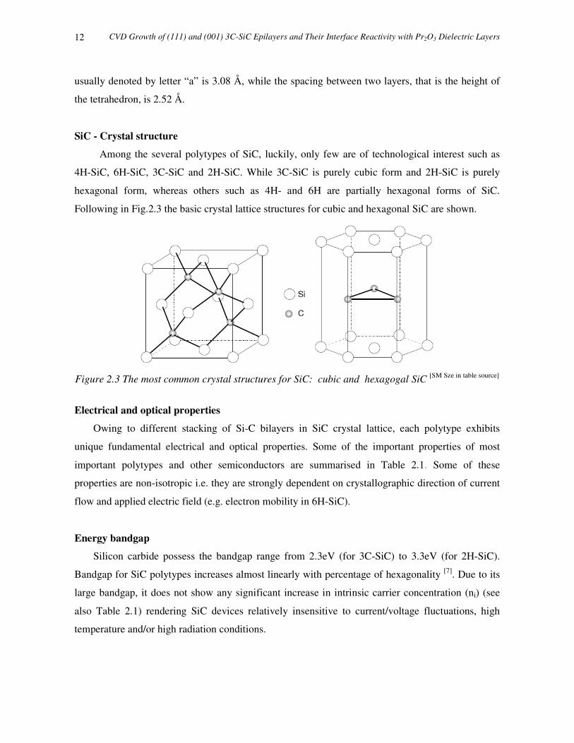
SiC - Crystal structure
Among the several polytypes of SiC, luckily, only few are of technological interest such as
4H-SiC, 6H-SiC, 3C-SiC and 2H-SiC. While 3C-SiC is purely cubic form and 2H-SiC is purely
hexagonal form, whereas others such as 4H- and 6H are partially hexagonal forms of SiC.
Following in Fig.2.3 the basic crystal lattice structures for cubic and hexagonal SiC are shown.
Figure 2.3 The most common crystal structures for SiC: cubic and hexagogal SiC [SM Sze in table source]
Electrical and optical properties
Owing to different stacking of Si-C bilayers in SiC crystal lattice, each polytype exhibits
unique fundamental electrical and optical properties. Some of the important properties of most
important polytypes and other semiconductors are summarised in Table 2.1. Some of these
properties are non-isotropic i.e. they are strongly dependent on crystallographic direction of current
flow and applied electric field (e.g. electron mobility in 6H-SiC).
Energy bandgap
Silicon carbide possess the bandgap range from 2.3eV (for 3C-SiC) to 3.3eV (for 2H-SiC).
Bandgap for SiC polytypes increases almost linearly with percentage of hexagonality [7]. Due to its
large bandgap, it does not show any significant increase in intrinsic carrier concentration (ni) (see
also Table 2.1) rendering SiC devices relatively insensitive to current/voltage fluctuations, high
temperature and/or high radiation conditions.

2. Silicon Carbide and Dielectrics: Background 13
Breakdown electric field
Due to the large breakdown electric field of wide bandgap the devices fabricated from SiC will
operate more efficiently even at high voltages as compared to those from other materials.
Thermal conductivity
SiC is better thermal conductor than other currently used semiconductor materials which allows
(a) greater heat dissipation (reducing the need for cooling system design integration) and (b) stable
operation at higher temperatures.
Saturation electron drift velocity
SiC’s higher electron saturation drift velocity allows an increase in frequency switching
capability and a decrease in power loss during circuit switching, as compared to current
semiconductor devices made of silicon or gallium arsenide [8].
The performance of most of the electronic devices is controlled by following major elements:
• The bandgap energy of the material: due to its large bandgap, SiC does not show any
significant increase in intrinsic carrier concentrates rendering SiC devices relatively
insensitive to current/voltage fluctuations and high temperature and/or high radiation
conditions
• Intrinsic carrier concentration and/or doping level
• The electron/hole effective masses and
• The carrier mobility

CVD Growth of (111) and (001) 3C-SiC Epilayers and Their Interface Reactivity with Pr2O3 Dielectric Layers
14
Table. 2.1
Comparison of properties of selected SiC polytypes with other main semiconductors (at 300K)
Property Si GaAs GaN(H) 4H-SiC 6H-SiC 3C-SiC
Bandgap (eV) 1.12 1.42 3.42 3.2 3.0 2.3
Breakdown electric field
@ ND=1017cm-3 (MVcm-1)
c-axis:3.2׀׀ c-axis:3.0׀׀ 5~ 0.6 0.6
c-axis:>1
>1.5
Thermal conductivity (Wcm-1K-1) 1.5 0.46 ~2.25,6,7 3-5 3-5 3-5
Intrinsic carrier concentration (cm-3) 1010 1.8x10⁶ ~10-10 ~10-7 ~10-5 ~10-1
Saturated electron velocity (107cm s-1) 1.0 1.2 2.04 2 2 2.5
Electron mobility
@ ND=1016cm-3 (cm2V-1 s-1)
1200 6500 5003
@1017
c-axis:800׀׀
c-axis:800
c-axis:60׀׀
c-axis:400
750
Hole mobility @ NA=1016cm-3 (cm2V-1
s-1)
420 320 350 115 90 40
Maximum operating temperature (°C) 300 460 1240 800
Relative dielectric constant 11.9 13.1 10.4 (a)
9.5 (c)
9.7 9.7 9.7
Lattice constant (Å) 5.43 5.65 a=3.189
c=5.1851
a=3.073
c=10.053
a=3.080
c=15.117
4.36
Sources in reference [9]
2.3 SiC: Electronic Band structures
In semiconductor crystals there exists a periodic potential with the periodicity of the lattice. It is
the quantum mechanical interaction of electrons with the periodic potential of the lattice that gives
rise to the band structure of solids i.e. allowed energy bands in which electrons can exist, satisfying
Pauli’s exclusion principle, separated by forbidden energy regions. Usually the band structure of a
crystalline solid is obtained by solving the Schrödinger equation of an approximate one-electron
problem. Using the Bloch theorem one can show that the energy Ek is periodic in the reciprocal
lattice, Ek=Ek+G where G is the reciprocal lattice vector. So, for a given band index, to label the
energy uniquely, it is sufficient to use only k’s in a primitive cell of the reciprocal lattice. The
standard convention is to use the Wigner-Seitz cell in the reciprocal lattice, called Brillouin zone. It
is thus evident that we can reduce any momentum k in the reciprocal space to a point in the
Brillouin zone, where any energy state can be given a label in the reduced zone schemes.
Fig.2.4 shows the band structures of 3C and 2H-SiC both represented in 2H Brillouin zone [11].
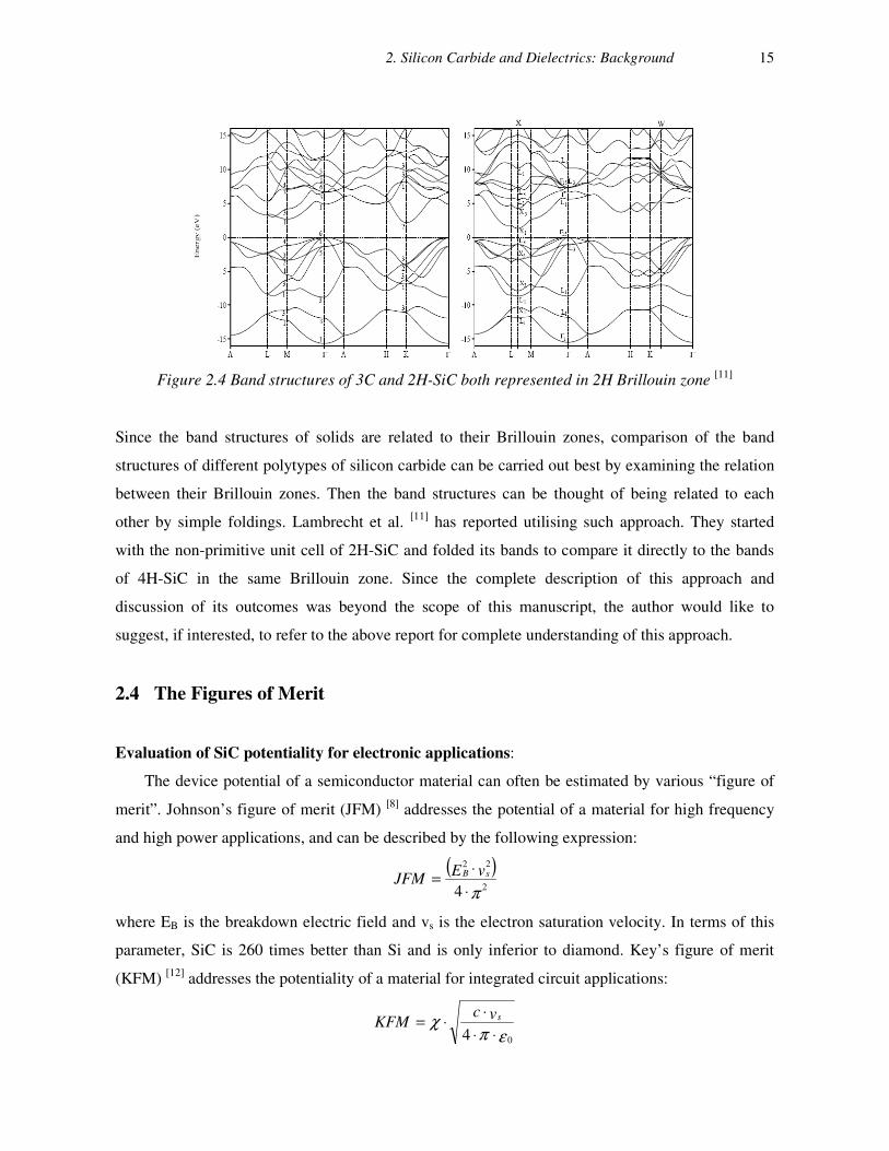
2. Silicon Carbide and Dielectrics: Background 15
Figure 2.4 Band structures of 3C and 2H-SiC both represented in 2H Brillouin zone [11]
Since the band structures of solids are related to their Brillouin zones, comparison of the band
structures of different polytypes of silicon carbide can be carried out best by examining the relation
between their Brillouin zones. Then the band structures can be thought of being related to each
other by simple foldings. Lambrecht et al. [11] has reported utilising such approach. They started
with the non-primitive unit cell of 2H-SiC and folded its bands to compare it directly to the bands
of 4H-SiC in the same Brillouin zone. Since the complete description of this approach and
discussion of its outcomes was beyond the scope of this manuscript, the author would like to
suggest, if interested, to refer to the above report for complete understanding of this approach.
2.4 The Figures of Merit
Evaluation of SiC potentiality for electronic applications:
The device potential of a semiconductor material can often be estimated by various “figure of
merit”. Johnson’s figure of merit (JFM) [8] addresses the potential of a material for high frequency
and high power applications, and can be described by the following expression:
( )π
2
22
4 ⋅
⋅=
vEJFM
sB
where EB is the breakdown electric field and vs is the electron saturation velocity. In terms of this
parameter, SiC is 260 times better than Si and is only inferior to diamond. Key’s figure of merit
(KFM) [12] addresses the potentiality of a material for integrated circuit applications:
επχ
04 ⋅⋅
⋅⋅=
vcKFM s

CVD Growth of (111) and (001) 3C-SiC Epilayers and Their Interface Reactivity with Pr2O3 Dielectric Layers
16
where c is the velocity of light, ε 0 is the static dielectric constant and χ is the thermal conductivity.
In terms of this figure of merit, SiC is 5 times better than Si and is again, only second to diamond.
Baliga’s figure of merit (BFM) [13] defines materials parameters to minimize the conduction loss in
low-frequency unipolar transistors.
EBFM g3
0 ⋅⋅= µε
Here µ is the mobility and Eg is the bandgap of the semiconductor
Table 2.2 Relative figures of merit of different semiconductors [14]
Si GaAs 3C-SiC(4H) Diamond Relative ZJ 1 7 1130(262) 2601 Relative ZK 1 0.5 6(5.1) 32 Relative ZB 1 2.6 (2400) 1x10⁵
2.5 3C-SiC Surfaces
Surfaces and interfaces are usually the most reactive regions of any material. There is a large
lattice mismatch between Silicon carbide and silicon. The thin film epigrowth on lattice mismatched
substrates induces not only a poor control of growth, formation of point and extended defects, but
also low reproducibility of doping, metallisation, surface preparation and stoichiometry. Extensive
work has been done on macroscopic bulk defects of cubic silicon carbide layers grown by chemical
vapor deposition. There have been some efforts on the quality of reconstructed surfaces and their
correlation with the bulk defects. Surface quality is also important for any device fabrication, e.g. a
very smooth sample exhibit an unusual 4x4 Si-terminated structure [15] and rough surfaces are even
more difficult to clean [16]. Ion bombardment and subsequent annealing was unsuccessful [17, 18] for
preparing well-ordered and stoichiometric SiC(001) surfaces partially due to different Si and C
sputtering rates, Si desorbed rapidly well below the temperatures needed to repair the lattice
damages leading to high graphitic carbon concentration[19]. An alternate method, UHV annealing,
has been used for a good surface preparation. Since the existing O impurities desorb as SiO during
UHV annealing, leading to Si-deficient surface with excess graphitic carbon. This problem has been
easily solved by preparing the Si rich SiC surface just after the growth. It is very difficult to avoid
graphitic carbon formation in preparing a C-terminated surface by UHV annealing.
Low temperature in-situ chemical cleaning techniques have been developed by Kaplan [20, 21]
1) depositing Ga metal and later thermal desorption. The graphitic carbon floats on Ga metal

2. Silicon Carbide and Dielectrics: Background 17
surface and carried away during desorption, along with oxides formed by reaction of Ga with O,
probably aided by the high heat of formation of Ga2O3 versus SiO2 and SiO. 2) The second
approach is heating the samples in Si-vapor from a resistively heated Si wafer. The O impurity
desorbs as SiO, and the loss of Si is compensated by incident flux, while graphitic carbon reacts to
form SiC. The main advantage of this method is that graphitised or otherwise contaminated surfaces
can be easily converted to pure SiC phase. Ballina et al. [22] used ion bombardment to remove O and
metallic Cr deposition and annealing at 750°C. Annealing for Cr carbide which desorbs above
750°C, leaving well ordered Si-terminated (2x1) surfaces. Silicon carbide exhibit a (2x1) LEED
pattern for heat cleaned, Si flux-annealing and high temperature Si2H6 (disilane) dosed c(2x2) C
terminated surfaces. Hara et al. [23] studied the full range of (001) reconstructions using medium
energy ion scattering (MEIS) and found that (2x1) corresponds to termination in a full monolayer
(ML) of Si. Powers et al. [24] have proposed the buckled dimmer model from (2x1) LEED structural
analysis. Soukiassian et al. [25] reported that (2x1) occurs for high density of defects, such as
missing dimers.
The c(4x2) occurs for very well ordered terminating Si (ML) [25, 26] , which can be formed
from the (2x1) by controlled deposition of Si. In XPS Si2p core level, (2x1) shows a larger
inhomogeneous broadening and a larger band bending than other reconstructions, implying the
presence of higher density of surface defects [27]. Many groups have used C1s core level to study
near surface compositional changes in SiC [27]. Asymmetry towards higher binding energy suggests
a second component in addition to bulk C1s. Since a perfect (2x1) surface, terminate in a full ML of
Si, is not expected to show significant surface induced C1s binding energy shift, this suggests Si-
vacancies in the “real” (2x1) reconstruction. This extra feature is absent for c(4x2) [26].
2.6 SiC Oxidation
SiC has one great advantage over other III-V and II-VI wide bandgap semiconductors; that an
oxide layer can be thermally grown by heating in O2 ambient exactly like for Si. This oxide layer is
used as gate isolation material for metal oxide semiconductor field effect transistor MOSFET,
which is a most widely used semiconductor device in modern electronic industry. Several groups
have reported the fabrication of MOSFETs in three main polytypes 4H, 6H [28-32] and 3C-SiC [33]
however, the channel mobility is extremely small compared to its bulk value which hinders the
realisation of power MOSFET in SiC.

CVD Growth of (111) and (001) 3C-SiC Epilayers and Their Interface Reactivity with Pr2O3 Dielectric Layers
18
The oxide semiconductor interface layer plays an important role in the performance and
reliability of MOSFETs and therefore a high quality SiO2 layer formation, with a low defect density
at the interface, is a crucial fabrication step. This is because the mobility of charge carriers is
significantly affected by the existing defects at the interface over the channel region (Fig.2.4). The
oxidation rate of SiC is in general lower that that of Si by more than an order of magnitude.
Therefore, temperatures exceeding 1100°C are typically used in the dry oxidation process. The
SiO2/SiC interface defect densities obtained to date are relatively high and one limiting factor for
the formation of a high quality oxide is considered to be a carbon containing by-product at the
interface [34]. Several reports have pointed out [35-37] that silicon oxycarbide exists within the
thickness of 0.3-1nm at the interface. While, recent report revealed that there is no excess carbon in
the oxide or at the interface. However, the oxide is structurally different from that grown on Si
though the oxide is stoichiometric SiO2 [38]. In addition, Si-Si bonds remain at the interface after CO
loses during oxidation process [39]. From the above discussion, one could say that the obvious proof
for inferior MOS properties of SiC has not been identified yet.
Figure2.4 Schematic of a typical MOSFET Structure
X-rays photoelectron studies of Si-SiO2 interfaces have identified an interfacial compositional
transition layer within 0.5nm of the interface which contains intermediate oxidation states of Si viz.
Si+1, Si+2 and Si+3. These transition regions can contribute to interface roughness and also give rise
to electronically active defects. Improvement in the device performance is achieved by post-
oxidation annealing which reduces sub-oxide bonding groups in interfacial transition region,
effectively smoothing the Si-SiO2 interface [40-44]. Investigations of SiC-SiO2 interfaces have also
identified an interfacial compositional transition layer [45]. Since SiC has wide bandgap, the
intermediate oxidation states exist within the bandgap and consequently affecting the device
performance. Due to the dissimilar transitional layer at the SiC-SiO2 interface, the interface state
density Dit is found to be much higher than that at the Si-SiO2 interface. Presence of so high
interface states density is generally attributed to carbon clusters and near-interfacial defects in the
oxide layer [46]. Theoretical investigation has confirmed that the emission of CO molecules during
Spacer Gate Oxide Gate electrode
Channel Source Drain

2. Silicon Carbide and Dielectrics: Background 19
SiC oxidation can lead to carbon cluster formation [47]. Much effort has been devoted to the
improvement of the interface quality between SiC and its native oxide. Promising processes for the
reduction of the interface-state density are re-oxidation [48] or annealing in ammonia [49]. These
processes should remove carbon from the interface [50] or passivate carbon-cluster gap states by N
incorporation [51].
The density of interface states Dit at SiO2 interface with the three most common SiC polytypes
(3C, 6H and 4H both n and p-type), oxidised in dry O2, remains above 1011 cm-2 eV-1 over the entire
SiC bandgap energy range, measured by “Constant Capacitance-Deep Level Transient
Spectroscopy” (CC-DLTS) [52]. In the lower half of the bandgap Dit is in the range of 1012 cm-2 eV-1
and in the vicinity of conduction band edge, particularly in 4H-SiC, it approaches 1013 cm-2 eV-1.
Other type of measurement techniques, e.g. C-V measurements, indicates that p-type SiC MOS
structures show much higher Dit in the vicinity of the Fermi level than the n-type ones [53, 54]. This
was thought to be associated with Al dopants typically used as acceptor dopants in SiC. Moreover
over-compensation of Al-doped p-SiC into n-type SiC by nitrogen ion implantation results in a
similar interface quality as in Al-free n-type SiC MOS structures [55]. A high value of Dit is observed
near the conduction band of 4H, lower in 6H and no Dit in 3C-SiC MOS structures [56] perhaps due
to different conduction band (CB) edges for different polytype. Dit is also observed to be strongly
dependent on the crystallographic orientation of the oxidised planes. It increases with increasing
misalignment angle from the (0001) plane Si-surface due to higher defect density at the misaligned
surfaces [57]. The MOS structures on other faces, like (11-20) and (1-100), exhibit much higher Dit
in the lower portion of the band gap which was associated with the higher availability of carbon
atoms at these SiC surfaces.
2.7 Alternate dielectrics on SiC
Due to the presence of high density of interface states, at SiO2/SiC interface, besides
insufficient stability of oxides electrical properties at elevated temperatures and in high electric
fields there is a possibility of the application of alternate dielectric materials. The electrical
performance of several alternate dielectrics including AlN, AlON and Al2O3 on SiC is thoroughly
investigated by Lipkin et al. [58] reporting that alternate dielectric possess the problem of significant
leakage currents comparative to the buried silicon oxynitride between top and bottom SiO2 layers
on SiC. The Al based oxynitride (AlON) performance [59] was reported to be similar to that of
Al2O3. Several attempts have been made to use Al-based insulating materials, like AlN and Al2O3

CVD Growth of (111) and (001) 3C-SiC Epilayers and Their Interface Reactivity with Pr2O3 Dielectric Layers
20
as a replacement for SiO2 however they provide no substantial improvements as compared to SiO2,
and suffer both from the high Dit and substantial leakage current [60-63]. This is due to insufficient
barrier height to block electron/hole injection because of their lower bandgap [64-66]. The band offset
values between alternate dielectrics and SiC polytypes was calculated in [67]. All the dielectrics have
reduced valence band offsets at the interface with SiC as compared to SiO2 which implies lower
barrier height and consequently, under negative bias, large leakage currents. The solution to the low
valence band offset is the insertion of thin layer of classical dielectric SiO2 between SiC and the
alternate dielectric [67]. This approach has been tested using HfO2 on SiC with SiO2 interlayer which
shows large suppression of leakage current comparative to that in the structure with HfO2 deposited
immediately on clean SiC surface [68]. This approach is further supported by the CV analysis of
SiC/insulator interface properties [69].
The Pr2O3 reacts with SiO2 on SiC or silicon forming Pr-silicate, Pr-silicides and if SiO2 is too
thin graphitic carbon at the interface [70, 71]. The presence of Pr-silicide, being metallic in nature, can
also assist in the increase in leakage current and presence of graphitic carbon would affect the
channel mobility. A short term solution to above problems is the controlled fabrication of Pr-silicate
prior to Pr2O3 growth which also assists [72] in formation of pure Pr2O3 phase by stopping Si out-
diffusion. Here the Pr-silicate formation does not solve the problem of low band offsets of Pr2O3
with SiC. The aluminum base dielectric layers are investigated by several groups. The reported
conduction and valence band offsets for aluminum nitride to SiC [73] are 1.7eV and 1.3eV
respectively.
2.8 References
1. Ramsdell R. S., “Studies in Silicon Carbide”, American Mineralosists, vol.32, (1947), pp64-82
2. Verma A. R. and P. Krishna, “Polymorphism and Polytypism in crystals”, J. Wiley & Sons Inc.
New York 1966, p.106
3. Backes W.H., P.A. Bobbert, and W. van Haeringen, “Energy-band structure of SiC polytypes
by interface matching of electronic wave functions” Physical Review B 49, (1994) p.7564
4. Haeringen W. van, P. A Bobbert, and W.H. Backes, “On the Band Gap Variation in SiC
Polytypes”, Physica Status Solidi (b) 202 (1997) p.63
5. Wenzien B., P. Käckell, F. Bechstedt, and C. Cappellini, “Quasiparticle band structure of
silicon carbide polytypes” Physical Review B 52,(1995) p.10897

2. Silicon Carbide and Dielectrics: Background 21
6. Choyke W. J., D. R. Hamilton and L. Patrick, “Optical Properties of Cubic SiC: Luminescence
of Nitrogen-Exciton Complexes, and Interband Absorption” Physical Review 133 (1964)
p.A1163
7. Bandgap for SiC polytypes increase almost linearly with the percentage of hexagonality [6]
8. Keyes R. W., “Figure of merit for semiconductors for high-speed switches” Proceedings of
IEEE (1972) p.225
9. Table Sources:
Sze S. M., Physics of Semiconductor Devices, 2nd
edition, (1981) Wiley-Interscience, New York
Harris G. L., 1995 Properties of SiC, Insttitute of Electrical Engineers, London
Choyke W. J., H Matsunami, G Pensl 1997 Silicon Caribide-A Review of Fundamental
Questions and Applications to Current Device Technology, Wiley-VCH, Berlin
Pensl G., H Morkoc, B Monemar, E Janzen 1998, Silicon Carbide, III-Nitrides, and Related
Materials Materials Science Forum 264 – 8, Trans Tech, Switzerland.
1. Maruska H. P., and J. J. Tietjen, “The preparation and properties of vapor-deposited single-
crystal-line GaN”, Applied Physics Letters 15 (1969) p.327
2. Vergaftman I, Meyer, JR, and Rammohan LR, “Band parameters for III–V compound
semiconductors and their alloys” Journal Applied Physics 89, (2001) pp5815-5875
3. Abdel-Motaleb M. Ibrahim and R. Y. Korotkov, “Modeling of electron mobility in GaN
materials”, Journal of Applied Physics 97 (2005) p. 093715
4. Kolnik J, IH Oguzman, KF Brennan, R Wang, PP Ruden, and Y Wang, “Electronic
transport studies of bulk zincblende and wurtzite phases of GaN based on an ensemble onte
Carlo calculation including a full zone band structure”, Journal of Applied Physics 78
(1995) p.1033
5. Zau J., D kotchetkov and AA Balankin “Thermal conductivity of GaN films: Effects of
impurities and dislocations” Journal of Applied Physics 92, (2002) p.2534
6. Kotchetkov D., J Zou and AA Balandin “Effect of dislocations on thermal conductivity of
GaN layers” Applied Physics Letters 79 (2001) p.4316
7. Florescu D. I., V. M. Asnin, F. H. Pollak, “High spatial resolution thermal conductivity and
Raman spectroscopy investigation of hydride vapor phase epitaxy grown n-GaN/sapphire
(0001): doping dependence” Journal of Applied Physics 88, (2000) p.3295
10. Bechstedt F., Käckell P., Zywietz A., Karch K., Adolph B., Tenelsen K., Furthmüller J.,
“Polytypism and Properties of Silicon Carbide” Physica Status Solidi (b) 202, (1997) p.35

CVD Growth of (111) and (001) 3C-SiC Epilayers and Their Interface Reactivity with Pr2O3 Dielectric Layers
22
11. Lambrecht W. R. L., S. Limpijumnong, S. N. Rashkeev, B. Segall, “Electronic Band Structure
of SiC Polytypes: A Discussion of Theory and Experiment” Physica Status Solidi (b)202,
(1997) p.5
12. Johnson E. O., “Physical limitations on frequency and power parameters of transistors” RCA
Reviews (1965) pp.163-177
13. Baliga B. J., “Semiconductors for high-voltage, vertical channel field-effect transistors”
Journal of Applied Physics 53 (1982) p.1759
14. Davis R. F., “Thin films and device of diamond, silicon carbide and gallium nitride” Physica B
185 (1992) pp1-15
15. Kaplan R. “Summary Abstract: Surface structures of β-SiC and pseudomorphic Si adlayers”,
Journal Vacuum Science & Technology A 6, (1989) p.829
16. Kaplan R. and Parrill T. M. “Reduction of SiC Surface Oxides by A Ga Molecular Beam:
LEED and Electron Spectroscopy Studies”, Surface Science 165 (1986) ppL45-L52
17. Kaplan R., “Surface studies of epitaxial β-SiC on Si(001)” Journal of Applied Physics 56,
(1984) p.1636
18. J. J. Bellina Jr., J. Ferrante, and M. V. Zeller, “Surface modification strategies for (100)3C-
SiC”, Journal of Vacuum Science & Technology A4, (1986) p.1692
19. Ballina J.J., Zeller, Jr. M.V. “Stoichiometric changes in the surface of (100) cubic SiC caused
by ion bombardment and annealing” Applied Surface Science 25 (1986) pp.380-390
20. Kaplan R., “Surface structure and composition of β- and 6H-SiC” Surface Science 215, (1989)
p.111
21. R. Kaplan and T. M. Parrill, “Reduction of SiC surface oxides by a Ga molecular beam: LEED
and electron spectroscopy studies” Surface Science 165, (1986) p.L45
22. Bellina J. J., Jr., J. Ferrante, M. V. Zeller, “ Surface modification strategies for (100)3C-SiC”
Journal of Vacuum Science & Technology A4, (1986) p.1692
23. Hara S, W. F. J. Slijkerman, J.F.van der Veen, I. Ohdomari, S. Misawa, E. Sakuma, and S.
Yoshida, “Elemental composition of β-SiC(001) surface phases studied by medium energy ion
scattering” Surface Science 231, (1996) p.L196
24. Powers J. M., A. Wander, M. A.Van Hove, and G. A. Somorjai, “Structural analysis of the β-
SiC(100)-(2x1) surface reconstruction by automated tensor LEED” Surface Science 260,
(1992) p.L7
25. Soukiassian P., F. Semond, L. Douillard, A. Mayne, G. Dujardin, L. Pizzagalli, and C. Joachim,
“Direct Observation of a β-SiC(100)- c(4x2) Surface Reconstruction” Physical Review Letters
78, (1997) p.907

2. Silicon Carbide and Dielectrics: Background 23
26. Shek M.L., “Soft X-ray studies of a c(4x2)* β-SiC(100) surface” Surface Science 349, (1996)
p.317
27. Shek M.L., K.E. Miyano, Q.-Y. Dond, T.A. Callcott, and D. L. Ederer, “Preliminary soft x-ray
studies of β-SiC” Journal of Vacuum Science and Technology A 12, (1994) p.1079
28. Spitz J., M.R. Melloch, J.A. Cooper Jr., M.A. Capano, “2.6kV 4H.SiC lateral DMOSFETs”
IEEE Electron Device Letters. 19 (1998) p.100
29. Weitzel C. E., J.W. Palmour, C.H. Carter Jr., K. Moore, K.J. Nordquist, S. Allen, C. Thero, M.
Bhatnagar, “Silicon carbide high-power devices” IEEE Transactions on Electron Devices 43
(1996) p.1732
30. Shenoy J. N., J.A. Cooper Jr., M.R. Melloch, “High-voltage double-implanted power
MOSFET’s in 6H-SiC” IEEE Electron Device Letters 18 (1997) p.93
31. Avila R. E., J. J. Kopanski and C. D. Fung, “Behavior of inversion layers in 3C silicon
carbide” Applied Physics Letters 49 (1986) p.334
32. Materials Research Society Symposium Proceedings 54 (1986) p561, 97 (1987) p2597, 116
(1988) p.357
33. Ohshima T., K. K. Lee, Y. Ishida, K. Kojima, Y. Tanaka, T. Takahashi, M. Yoshikawa, H.
Okumura, K. Arai and T. Kamiya, “The electrical characteristics of Metal-oxide-semiconductor
field effect transistors fabricated on cubic silicon carbide”, Japanese Journal of Applied
Physics 42 (2003) ppL625-L627
34. Afanas’ev V.V., M. Bassler, G. Pensl, M. Schulz, “Intrinsic SiC/SiO2 Interface States” Physica
Status Solidi (a) 162 (1997) p.321
35. Hormetz B., H.-J. Michael, J. Halbritter, “Oxidation and 6H-SiC-SiO2 interfaces”Journal
Vacuum Science and Technology A 13 (3) (1995) p.767
36. H. Tsuchida, I. Kamata, K. Izumi, “Chemical States of Crystalline Silicon Carbide Surface”
Japanese Journal of Applied Physics 34 (1995) p.6003
37. C. Önneby, C.G. Pantano, “Silicon oxycarbide formation on SiC surfaces and at the SiC/SiO2
interface” Journal Vacuum Science and Technology A 15 (3) (1997) p.1597
38. Jernigan G., R.E. Stahlbush, M.K. Das, J.A. Cooper Jr., L.A. Lipkin, “Interfacial differences
between SiO2 grown on 6H-SiC and on Si(100)” Applied Physics Letters 74 (1999) p.1448
39. Jernigan G. G., R.E. Stahlbush, N.S. Saks, “Effect of oxidation and reoxidation on the oxide-
substrate interface of 4H- and 6H-SiC” Applied Physics Letters 77 (2000) p.1437
40. Keister J. W., J. E. Rowe, J. J. Kolodziej, H. Niimi, H. –S. Tao, T. E. Madey and G. Lucovsky,
“Structure of ultrathin SiO2 /Si(111) interfaces studied by photoelectron spectroscopy” Journal
of Vacuum Science and Technology A17 (1999) p.1250

CVD Growth of (111) and (001) 3C-SiC Epilayers and Their Interface Reactivity with Pr2O3 Dielectric Layers
24
41. Chen X., J. M. Gibson, “Dramatic effect of postoxidation annealing on (100)Si/SiO2
roughness” Applied Physics Letters 70 (1997) p.1462
42. Lucovsky G., A. Banerjee, H. Niimi, K. Koh, B. Hinds, C. Meyer, G. Lüpke and H. Kurz,
“Elimination of sub-oxide transition regions at Si-SiO2 interfaces by rapid thermal annealing at
900°C” Applied Surface Science 117 (1997) p202
43. Ishikawa K., Y. Uchiyama, H. Ogawa and S. Fujimura, “Dependence of TO and LO mode
frequency of thermally grown silicon dioxide films on annealing temperature” Applied Surface
Science 117 (1997) p212
44. J. G. Lucovsky, A. Banerjee, B. Hinds, B. Claflin, K. Koh, and H. Yang “Minimization of
suboxide transition regions at Si-SiO2 interfaces by 900 °C rapid thermal annealing” Journal of
Vacuum Science & Technology B 15 p.1074
45. Önneby C. and C. G. Pantano ”Silicon oxycarbide formation on SiC surfaces and at the
SiC/SiO2 interface” Journal of Vacuum Science & Technology A 15 (1997) p1597
46. Afanas’ev V. V. and A. Stesmans M. Bassler, G. Pensl, and M. J. Schulz C. I. Harris,
“Elimination of SiC/SiO2 interface states by preoxidation ultraviolet-ozone cleaning”, Applied
Physics Letters 68 (1996) p.2141
47. Ventra M. Di and S. T. Pantelides “Atomic-Scale Mechanisms of Oxygen Precipitation and
Thin-Film Oxidation of SiC”, Physics Review Letters 83 (1998) p.1624
48. Das M. K., J. A. Cooper, Jr. and M. R. Melloch, “Effect of Epilayer characteristics and
Processing Conditions on the Thermally Oxidized SiO2/SiC Interface” Journal of Electronic
Materials 27 (1998) p.353
49. Chung G. Y., C. C. Tin, and J. R. Williams K. McDonald, M. Di Ventra, S. T. Pantelides, and
L. C. Feldman R. A. Weller, “Effect of nitric oxide annealing on the interface trap densities
near the band edges in the 4H polytype of silicon carbide” Applied Physics Letters 76 (2000)
p.1713
50. Lipkin L. A., and Palmour J. W., “Effect of Epilayer Characteristics and Processing Conditions
on the Thermally Oxidized SiO2/SiC Interface”, Journal of Electronic Materials 25 (1996)
p.909
51. Chung G. Y., C. C. Tin, J. R. Williams, K. McDonald, M. Di Ventra, R. K. Chanana, S. T.
Pantelides, and L. C. Feldman R. A. Weller, “Effects of anneals in ammonia on the interface
trap density near the band edges in 4H–silicon carbide metal-oxide-semiconductor capacitors”
Applied Physics Letters 77 (2000) p.3601

2. Silicon Carbide and Dielectrics: Background 25
52. Afanas’ev VV, F. Ciobanu, G. Pensl, and A. Stesmans, “Constant Capacitance Deep Level
Transient Spectroscopy Contributions to the density of interface states in SiC MOS structures”
SiC Recent Major Advances, Springer , ISBN-3540404589 pp343-371
53. Afanas’ev V. V., M. Bassler, G. Pensl, and M. J. Schulz;” Intrinsic SiC/SiO2 Interface States”
Physica Status Solidi A 162, (1997) p.321
54. Dev Alok, P. K. McLarty, and B. J. Baliga, “Electrical properties of thermal oxide grown using
dry oxidation on p-type 6H-silicon carbide” Applied Physics Letters 65, (1994) p.2177
55. Bassler M., Valeri V. Afanas'ev, Gerhard Pensl “Interface State Density at Implanted 6H-
SiC/SiO2 MOS Structure”, Materials Science Forum 264-268, (1998) p.861
56. Ciobanu F., G. Pensl, H. Nagasawa, A. Schöner, S. Dimitrijev, K. Y. Cheong, V. V. Afanas’ev
and G. Wagner, “Traps at the Interface of 3C-SiC/SiO2-MOS Structures” Materials Science
Forum 433-436, (2003) p.551
57. Frédéric Lanois, Dominique Planson, P. Lassagne, C. Raynaud, E. Bano, “6H-SiC MOS
Capacitors on Sloped Surface: Realisation Characterisatio and Electrical Results” Materials
Science Forum 264-268, (1998) p.1029
58. Lipkin L.A., and J. W. Palmour, “Insulator Investigation on SiC for Improved Reliability”,
IEEE Transactions on Electron Devices 46 (1999) p.525
59. Chawdhury E. A., J. Kolodzey, J. O. Olowolafe, G. Qiu, G. Katulka, D. Hits, M.Dashiell, D.
van der Weide, C. P. Swann, and K. M. Unruh, “Thermally oxidized AlN thin films for device
insulators,” Applied Physics Letters 70 (1997) p.2732
60. Zetterling C.-M. and M. Stling N. Nordell O. Schön and M. Deschler “Influence of growth
conditions on electrical characteristics of AlN on SiC”, Applied Physics Letters 70 (1997)
p.3549;
61. Lipkin L.A., J. W. Palmour, “Insulator investigation on SiC for improved reliability”, IEEE
Trans Electron Devices ED-46 (1999) p.525
62. Lazar H. R., V. Misra, Johnson R.S. and G. Lucovsky “ Characteristics of metalorganic remote
plasma chemical vapor deposited Al2O3 gate stacks on SiC metal–oxide semiconductor
devices” Applied Physics Letters 79 (2001) p.973
63. Norio Onojima Jun Suda, and Hiroyuki Matsunami ” Molecular-beam epitaxial growth of
insulating AlN on surface-controlled 6H–SiC substrate by HCl gas etching” Applied Physics
Letters 80 (2002) p.76
64. W. M. Yim, E. J. Stofko, P. J. Zanzucchi, J. I. Pankove, M. Ettenberg and S. L. Gilbert
“Epitaxially grown AlN and its optical band gap” Journal of Applied Physics 44 (1973) p.292

CVD Growth of (111) and (001) 3C-SiC Epilayers and Their Interface Reactivity with Pr2O3 Dielectric Layers
26
65. PB Perry and RF Rutz” The optical absorption edge of single crystal AlN prepared by close-
spaced vapor process” Applied Physics Letters 33 (1978) p.319
66. V. V. Afanas’ev and A. Stesmans B. J. Mrstik C. Zhao ” Impact of annealing-induced
compaction on electronic properties of atomic-layer-deposited Al2O3” Applied Physics Letters
81 (2002) p.1678
67. Valeri V. Afanas'ev, M. Bassler, G. Pensl, A. Stesmans “Oxidation of Silicon Carbide:
Problems and Solutions” Materials Science Forum 389-393, (2002) p.961
68. Afanas’ev V.V., A. Stesmans, F. Chen, A Campbell, R. Smith, “HfO2-based insulating stacks
on 4H-SiC(0001)” Applied Physics Letters 82 (2003) p.922
69. Afanas’ev V.V., F. Ciobanu, G. Pensl, and A. Stesmans, “Contributions to the density of
interface states in SiC MOS structures”, SiC Recent Major Advances, ISBN-3540404589,
Springer pp343-371
70. Schmeißer D., G. Lupina, H.-J Müssig, “Interface reactivity of Pr and SiO2 at 4H-SiC(001)”,
Materials Science and Engineering B 118 (2005) pp19-22,
71. Lupina G., J. Dabrowski, P. Formanek, D. Schmeißer, R. Sorge, C. Wenger, P. Zaumseil, H.-J.
Müssig “Solid-State reaction between Pr and SiO2 studied by photoelectron spectroscopy and
ab initio calculations” Materials Science in Semiconductor Processing 7 (2004) pp215-220
72. Aspinall H.C., J. Gaskell, P.A. Williams, A. C. Jones, P. R. Chalker, P. A. Marshall, L. M.
Smith and G. W. Critchlow, “Growth of Praseodymium Oxide and Praseodymium Silicate Thin
Films by Liquid Injection MOCVD”, Chemical Vapor Deposition 10 (2004) pp83-89
73. Choi J., R. Puthenkovilakam, and J. P. Chang, “Band structure and alignment of AlN/SiC
heterostructure”, Applied Physics Letters 86 (2005) p.192101

3
Bulk and Thin Film Growth


Chapter 3
Bulk and Thin film growth
Introduction
In this chapter the silicon carbide crystal growth techniques for both bulk and thin film
growth have been discussed briefly. Various bulk growth techniques for SiC are discussed followed
by a brief summary of to date progress on bulk growth. Then the SiC thin films growth techniques
are discussed briefly, simultaneously some of the imported reported work are also discussed. The
chemical vapour deposition technique has been discussed in detail followed by a brief summary of
important achievements in CVD growth of cubic silicon carbide.
3.1 Bulk Growth
Commercially, most of the semiconductor crystals, e.g. Si and GaAs, are grown using of the
various methods, such as Czochralski, liquid-encapsulated Czochralski, Bridgman, and gradient
freeze methods. To employ fully the advantage of the superior physical and electronic properties of
SiC devices, suitable bulk growth technique must be developed. Above mentioned usual methods
cannot be adopted for the growth of silicon carbide because of its high thermal stability. It can not
be melted under easily achievable process conditions, because it sublimes before melting. The
calculated values show that the stoichiometric SiC would melt only at above 100,000 atm and
3200°C. At high temperatures, above 1800°C it not only sublimes but dissociates in Si, C, SiC2 and
Si2C [1]. Because of these reasons, single crystals of SiC are grown using the techniques based on
vapor growth, high temperature solution growth, and their variants. Since SiC readily sublimes,
physical vapor growth can be easily adapted, and has become the primary method for growing large
sized SiC boules. The main three types of commercially used bulk growth techniques are Acheson
process, the Lely process and the modified Lely process. The last two of these processes require the
sublimation of a SiC source placed in the hot zone of the growth furnace and the subsequent mass
transport of vapor species to a cooler region, where the crystal grows by deposition from the vapor
phase. Source materials can be SiC powder, Si and C powder or crystalline SiC and the growth can
be seeded or unseeded. The vapor transport can be performed either in vacuum or in a gas ambient
at a pressure between 10-6 and 20 Torr and the growth temperature range is 1600 to 2700°C.

CVD Growth of (111) and (001) 3C-SiC Epilayers and Their Interface Reactivity with Pr2O3 Dielectric Layers
28
3.1.1. Acheson process
In this process a trough-type furnace is used, in which a mixture of silica and carbon with a
small percentage of sawdust and common salt are heated to about 2700°C. The result is a
combination of crystallites and polycrystalline agglomerates in different states of perfection, but
heavily contaminated due to the low purity of the source material. This kind of technique is mostly
used for the production of SiC for grinding applications; crystal quality is too less to be used for
substrate production in semiconductor industry.
3.1.2. Lely Process
This was the first technique for the production of electronic grade semiconducting SiC
developed by Lely in 1955 [2]. In this process SiC powder is sublimated at temperatures 2550-
2600°C in a closed graphite crucible filled with argon where spontaneous nucleation of crystals
occurs on perforated graphite wall cavities. A temperature gradient across the perforated graphite is
impressed in the above mentioned rang in order to initiate nucleation. The primary drawback of the
Lely process was small size of grown crystals, up to 10mm diameter. Furthermore, the grown
material shows poor control of the nucleation, non uniformity in doping and a distribution of
crystals of different size and polytypes, mainly 6H-SiC (75-95%), 4H, 15R and less frequently, 8H,
21R and 33R. This material is often used for research purposes, but the irregularity of the platelet
shape and the small size makes it not viable for electronic applications.
The original Lely method was later improved by Hamilton and others [3]. In this improved
version, SiC charge is packed in between the two annular graphite cylinders. The outer cylinder is
thick and the inner cylinder is thin and porous, which acts as a diaphragm. The sublimed SiC vapor
passes through the small holes in the diaphragm and crystals are nucleated at the inner surface.
Thick layers of SiC are also deposited on the lids at both ends. This modification offers slightly
better control over the number of nucleation sites and yield. Good quality, larger crystals are
obtained when the temperature variation in the cavity is small and the Ar pressure is maintained at
about one atmosphere
3.1.3. Modified Lely Process
Tairov and Tsvetkov in 1978 made a breakthrough in SiC bulk growth technology [4]. They
modified the Lely process, hence called modified Lely process, to grow large diameter bulk crystals

3. Bulk and Thin Film Growth 29
without the disadvantageous characteristic of the Lely process. In this technique a seed crystal is
introduced in the Lely chamber and growth proceeds by vapor transport of carbon and silicon,
placed in graphite crucible, bearing species from the source to the growth site. The necessary
condition for SiC growth using this approach is a temperature gradient between the source and the
seed, causing vapor phase transport of the species and their re-crystallisation on the seed crystal at
super-saturation condition. The typical growth pressure is less than 20 Torr, the growth temperature
between 2100 and 2400°C and the temperature gradient between the source and the seed 20 to
35°C/cm. The growth is usually performed on 0001 face (on-axis or with some offset angle) of
6H or 4H-SiC seed, Si or C face.
Figure 3.1 Schematics of SiC bulk growth methods: Acheson, Improved Lely[3]
and Modified Lely
Methods[4]
3.1.4. Control parameters of the bulk growth
Growth rate
Typical growth rates for the bulk growth of SiC are from0.5 to 1.2mm/h. A study of the
general theory of vapor-phase growth was developed by Lever [5] and Mandel
[6]; in this
development the growth rate is determined by the transport of the species from the source to the
seed either by diffusion or by the surface kinetics. This theory was applied to SiC growth by
Lilov[7], finding that the growth rate is limited by the rate of diffusive transport of the growing
species from the source to the growth surface and the diffusion constant of the gas species are
inversely proportional to the pressure in the deposition system. So the growth rate can be controlled
by changing the pressure in the deposition chamber.
SiC deposit
Graphite Crucible
SiC platelets
SiC lump
Graphite porous cylinder
Acheson Method
Amorphous SiC
SiC crystals nucleated in cavities
Carbon core with electrodes
Unreacted mixture
Improved Lely Method
Vapor flux
Source material
Seed
Modified Lely Method

CVD Growth of (111) and (001) 3C-SiC Epilayers and Their Interface Reactivity with Pr2O3 Dielectric Layers
30
Polytype control
The control of polytype is very important in bulk growth; in fact, if special precautions are not
taken, the inclusion of unwanted polytypes in the grown material is very common. There are many
factors which influence the polytype structure viz. growth temperature and pressure, surface
orientation, polarity of the seed and presence of impurities.
In the sublimation growth of SiC the polytype structure is mainly determined by the pumping
speed of the carrier gas, which directly influences the time dependence of the pressure in the growth
chamber. The time dependence of growth pressure can be described by the following equation:
P(t)=Peq+(P0-Peq)exp(-t/τ)
where P0 is the starting pressure, Peq is the final pressure and τ is the pumping speed constant, equal
to the ratio between the volume of the chamber and the pumping speed. A high τ value corresponds
to a low saturation and low initial growth rate and gives rise to 4H-SiC formation, a high τ value
gives rise to 3C-SiC formation and an intermediate τ value gives rise to 6H-SiC formation.
Also the polarity of the seed material (Si-type or C-type plane) and the presence of impurities
have an influence on the polytype determination. On (0001) C plane of 6H-SiC seed crystal the
crystal growth with boron as impurity leads to the 4H-SiC ingots, while on (0001) Si surface it
leads to 6H-SiC [8].
3.2 Thin film growth
Epitaxial thin film growth is a key process in SiC technology, since the bulk material quality
is too low for the direct use in device structures. It also makes possible the growth and further
processing, for device fabrication, at lower temperature with superior crystalline quality and better
doping control. Various techniques have been used for the epitaxial growth of SiC: chemical vapor
deposition, liquid phase epitaxy, sublimation epitaxy and molecular beam epitaxy. Different
problems are related to the growth of different polytypes on different substrates.
Here the detailed discussion of fundamentals of liquid phase epitaxy, sublimation epitaxy and
molecular beam epitaxy are beyond the scope of this thesis. The most utilised epigrowth technique,
chemical vapour deposition, is discussed, starting from fundamentals to its application for SiC
growth. Then the reported work on α-SiC epigrowth is reviewed followed by a discussion
emphasised on 3C-SiC epigrowth.

3. Bulk and Thin Film Growth 31
3.2.1. Molecular Beam Epitaxy
Molecular beam epitaxy is a technique for epitaxial growth via the interaction of one or
several molecular or atomic beams that occurs on a surface of a heated crystalline substrate. The
sources materials, solids (or gaseous supplied directly on substrate), are placed in evaporation cells
to provide an angular distribution of atoms or molecules in a beam. The substrate is heated to the
necessary temperature and, when needed, continuously rotated to improve the growth homogeneity.
In case of SiC, the first experiments on MBE were carried out with gaseous sources [9]
disilane (Si2H6) and ethylene (C2H4) at 1050-1250°C on 6H-SiC substrates mis-oriented by 3-4°.
Later experiments were also performed with solid sources [10], pyrolytic graphite and pure silicon,
evaporated by an electron gun.
Typical growth rates for both types of MBE are 0.03 - 0.3Ås-1 at a substrate temperature of
800°C – 1000°C. Generally 3C-SiC (CVD-material) on Si and 6H-SiC (Acheson-material) are used
as substrates. The main advantages are the low process temperature and high purity; the
disadvantages are low deposition rates and high cost of the MBE apparatus. Other problems are the
lattice damage caused by hydrogen and hydrocarbon incorporation into the deposited film and
additionally the strongly gas flow dependency of the polytype. Attempts to produce high quality
SiC single crystal layers thicker than 1 µm by this technique have not been successful.
3.2.2. Chemical Vapour Deposition
The process technology of chemical vapor deposition (CVD), today and for many years, has
been one of the key technologies in semiconductor processing. CVD technology is used throughout
the various processing steps in today’s semiconductor manufacturing; starting with the synthesis of
the elemental silicon through thin epitaxial and polycrystalline silicon films extending on through
the oxidation process, the deposition of dielectric films of nitrides, carbides, and silicides and
metallisation films.
Chemical vapor deposition: Basics
CVD is a materials synthesis process in which one more volatile precursors react in vapour
phase near or on heated substrate to form a solid thin film. The CVD technology combine several
scientific and engineering disciplines including thermodynamics, kinetics, fluid dynamics, plasma
physics (for plasma enhanced CVD) and of course the chemistry. Several steps that must happen in

CVD Growth of (111) and (001) 3C-SiC Epilayers and Their Interface Reactivity with Pr2O3 Dielectric Layers
32
every CVD process (Fig. 3.4) can be listed as follows: reactant gases are transported with carrier
gas to the reactor, reactant species diffuse through the boundary layer above the growth surface, the
species are transported to the surface via diffusion, reaction (adsorption or chemisorption) takes
place on the surface, gaseous byproducts are transported away from the surface, and finally diffused
away through the boundary layer.
Fluid Mechanics
The epitaxial layer uniformity is significantly influenced by the gas flow dynamics since the
successful uniform mass transport of precursors and reaction byproducts is dependent on consistent
flow conditions. The laminar flow ensures an even cooling load and controllable transport
phenomena in the reaction zone. Laminar flow is achieved when the fluid flows in smooth planes
stacked onto each other. The planes of flow do not mix and the only mechanism for species to travel
from one plane to another is diffusion [11, 12]. Because of the resistance of the surrounding surfaces, a
velocity distribution of the gas is observed where vmax is generally in the center of the reactor and
v=0 at the reactor walls. The so called “boundary layer” is the region where the v changes from that
of the bulk gas to zero. The boundary layer orientation with respect to the substrate surface
originates from the drag exerted by it on the gas flow. Since the reduction in the velocity increases
along the length of the heated substrate, the boundary layer becomes gradually thicker.
Figure 3.4 Schematic illustrating the fundamental steps in chemical vapour deposition
Bulk transport
Carrier gas
Reactant molecule
Reaction with film
Desorption
Diffusion of (g) byproduct
Bulk transport Of byproduct
Decomposition Transport across boundry layer
Adsorption
1
2
3
4
5
6
7
8
Surface diffusion

3. Bulk and Thin Film Growth 33
A rough estimation of laminar flow conditions can be made from the Reynolds number Re a
dimensionless parameter given as [13]
µ
ρν ..DR
re = . . . . . . . . . .(1)
where Dr is the diameter of the reactor tube, ν is the gas velocity, ρ is the gas density, and µ is
the gas viscosity. Usually in most of the industrial processes value of Re for CVD reactors is below
100, hence the gas flow is in laminar regime, since Re is less than 2000.
The thickness of boundary layer y is given as
=
R
xDy
e
r
21
. . . . . . . . . .(2)
where x is distance along the reaction chamber. So the boundary layer forms at the inlet of reaction
chamber and its thickness increases until the flow is fully established depending on total length of
reaction chamber.
The reactants are transported or diffuse across this boundary layer to reach the substrate
surface and the reaction by-products diffuse back across the boundary layer and are removed by the
main gas stream. The flux of species going to and coming from the substrate surface is given by
dy
dnDJ = and can be approximated to
( )
y
nnDJ
sg −= . . . . . . . . . .(3)
where ng and ns are the gas stream and surface reactant concentrations respectively; D is the gas
phase diffusivity which is a function of pressure and temperature. Under steady state condition the
flux of reactant to the substrate is equaled by the chemical reaction at substrate surface.
nkJ ss .= . . . . . . . . . .(4)
where ks is the reaction rate constant, therefore from eq.(3) and eq.(4)
hk
n
D
yk
nn
gs
g
s
g
s/11 +
=
+
= . . . . . . . . . .(4)
where hg=D/y gas phase mass transfer coefficient

CVD Growth of (111) and (001) 3C-SiC Epilayers and Their Interface Reactivity with Pr2O3 Dielectric Layers
34
So, the surface concentration of reactants ns, which determines the growth rate, is a function
of both, reaction chemistry and gas phase transport process. As y approaches zero, ns≈ng and the
growth process will be dominated by surface chemical reaction. If ks is very large relative to hg, the
surface concentration approaches zero, and the overall process is limited by the transport of
reactants across the boundary layer.
The slowest CVD process step from the above mentioned steps is rate determining step. When
CVD reaction rates for a particular chemistry and reactor geometry are plotted over reciprocal
temperature the deposition or growth rate varies exponentially with temperature and two regimes
are recognised as also shown in Fig.3.5.
• The kinetic or surface reaction rate controlled regime which occurs at lower
temperatures
• The diffusion or rate of arrival controlled regime which occurs at higher temperature.
This regime is also termed as mass transport controlled regime
Figure 3.5 Typical overall reaction rate for CVD reactors vs. reciprocal temperature[14]
Below some temperature, the surface reaction rate normally controls the growth rate, because
for a given reactor geometry, the rate of arrival is greater than the surface reaction rate. As the
temperature is increased, the overall surface reaction rate usually increases more rapidly than the
overall mass transport rate, and the rate of arrival or mass transport rate becomes the limiting factor.
103/T
Growth rate
Diffusion Controlled
Reaction rate Controlled

3. Bulk and Thin Film Growth 35
Depending on the type of source of supplying required activation energy, there are various
CVD processes viz. hot and cold wall CVD and plasma enhanced CVD etc. Pressure dependent
CVDs are atmospheric pressure CVD and low pressure CVD.
The CVD process is a viable single crystal production method with satisfactory doping
behavior. As discussed in the section dealing with the fundamentals of CVD, the precursor gases
are transported using a carrier gas, usually hydrogen, in a reactor on a substrate heated to specific
temperature where chemical reaction occurs on the surface of the substrate producing a solid
deposit on substrate, and volatile byproducts to be pumped away.
Through chemical vapour deposition thin films of SiC can be grown homoepitaxially (SiC on
the same polytype substrate) and heteroepitaxially (on different substrate TiC, Si etc.). Both types
of growth processes are described in the following sections.
3.2.2.1 SiC Homoepitaxy
First attempts of homoepitaxial growth of 6H-SiC on 6H-SiC substrates prepared by the
Acheson process were made at relatively high temperatures (1700-1900 °C) [15]. By improving the
substrate quality (modified Lely-process) the growth temperature was reduced. For example, 6H-
SiC grown on 6H-SiC Lely samples and 4H-SiC on 4H-SiC Lely samples, the process required
substrate temperatures of 1550°C or 1620°C respectively.
The growth rates of this process are 2µm.h-1. The n-type doping is done by N2, p-doping by
trimethylaluminium, with concentrations ranging from 1.1015 to 1.1019 m-3 [16, 17]. The Hall
measurements of n-doped 6H-SiC show an electron mobility of 104cm2(Vs)-1. High quality
materials are produced at low temperatures compared to 6H-SiC Lely material which has smaller
electron mobility. The high temperature CVD 6H-SiC epitaxial process provides deposition rates up
to 100 µm.h-1 [18], which is relatively high compared with LPE and sublimation processes.
Nishino et al. [19] reported on the 3C-SiC homoepitaxy deposition on 3C-SiC Lely-process
samples (SiH4/C3H8/H2) at a temperature of 1560 °C, atmospheric pressure with deposition rates of
2.5 µm.h-1, with nitrogen doping at a level of 5x1015cm-3. There are no significant DPB (double
positioning boundary) interface film defects by this method. The main problem in homoepitaxy of
SiC is the high production cost and lower quality due to high cost and lower quality of SiC
substrates compared to Si. The main advantages of homoepitaxy are the appropriate lattice

CVD Growth of (111) and (001) 3C-SiC Epilayers and Their Interface Reactivity with Pr2O3 Dielectric Layers
36
constants and thermal coefficients; beneficial only if high quality substrate can be produced
economically.
3.2.2.2 Heteroepitaxy: 3C-SiC
The advantages of using silicon as a substrate in heteroepitaxy of 3C-SiC are large size, high
quality, low price, and good polytype control. The equipment used in SiC heteroepitaxy is the same
as for homoepitaxy. Other substrates have also been investigated (TiC and Al2O3) [21-22], but they
are expensive or without adequate quality for SiC semiconductor applications. Thin films of 3C-SiC
on 6H-SiC growth at temperature of 1450 °C with deposition rates of 4µm.h-1 and thickness up to
12 µm were reported by Powell et al. [23]. Compared with 3C-SiC deposition on Si, these samples
exhibited fewer interface defects.
The initial experiments with deposition of SiC on Si [24-25] illustrated that differences in both
the lattice constant (almost 20%) and the thermal expansion coefficient (almost 8%) between SiC
and Si produced a high concentration of defects at the SiC-Si interface and consequently this
process of crystal growth turned out to be problematic. Nishino et al. [26] solved this problem by
growing films with the so called "Buffer layer" technique where the film is deposited at
atmospheric pressure with specific gases (SiH4/C3H8/H2) in a quartz reactor with a graphite
susceptor, and an inductive heating system. The Fig. 4.4 on p.52 shows the deposition process. The
growth occurs in two stages while H2 flow remains constant during the whole process.
This process was used by different research groups with some variations for 3C-SiC
deposition [16, 17, 27-35]. It was also tested with different Si substrates orientations and different gases.
The production of epitaxial films with high quality depends on number of factors. In particular, the
substrate orientation has large influence on the epitaxy process [36] and it has been shown that for
orientations (100) and (111) the best results are achieved. On the other hand, Si (111) substrates
frequently show cracks in the film during the cooling process because higher mechanical stresses
result for this substrate orientation compared to (100) substrates.
Exhaustive studies show that the deposition rate is connected with the quality of the film, i.e.
by using lower deposition rates, the quality is improved. In addition, when separate precursors are
used for Si and C, the proportion of Si and C (Si/C) in the gaseous phase changes the film
properties. Many authors used values from 0.4 to 1.0 [31, 37-39]. Other factors such as deposition
pressure, temperature, carbonisation deposition temperature, carbonisation duration and gaseous

3. Bulk and Thin Film Growth 37
purity influence the 3C-SiC film quality [33]. The Buffer-Layer-Process at temperatures higher than
1300 °C leads to the formation of several film crystal defects.
3.3 References
1. Lilov S. K., “Study of equilibrium processes in gas phase during silicon carbide
sublimation”, Materials Science Engineering B21 (1993) p.65
2. Lely J. A., “Darstellung von Einkristallen von Silicium Carbid und Beherrschung von
Art und Menge der eingebauten Verunreinigungen” Ber. Detsch. Kerm. Ges., 32, (1955)
pp229-231
3. Hamilton D. R., “The Growth of Silicon Carbide by Sublimation”, In: Connor J. R.,
Smilestens J., SiC A High Temperature Semiconductor, Pergamon, Oxford, (1960)
pp45-51
4. Yu. M., Tairov, V. F. Tsvetkov, “Investigation of growth processes of ingots of silicon
carbide single crystals” Journal of Crystal Growth 43 (1978) pp209-212
5. Lever R. F., “Transport of solid through the gas phase using a single heterogeneous
equilibrium”, Journal of Chemical Physics, vol.37, (1962) p.1174
6. Mandel G., “Surface limited vapor solvent growth of crystals”, Journal of Chemical
Physics, 40, (1964) p.683
7. Lilov D.S.K., Y. M. Tairov and V. F. Tsetkov, “Study of silicon carbide epitaxial
growth kinetics in the SiC-C system”, Journal of Crystal Growth 46, (1979) p.269
8. Avramenko S. F., V. S. Kiselev, M. Y. Valakh, V. G. Visotski, “Investigation of
structural perfection of SiC ingots grown by a sublimation method” Semiconductor
Physics, Quantum Electronics & Optoelectronics vol.2 (1999) pp.76-79, and references
therein
9. Rowland L. B., Kern R. S., Tanaka S. and Davis R. F., “Gas-source molecular beam
epitaxy of monocrystalline β-SiC on vicinal α(6H)-SiC”, Journal of Materials Research
8 (1993) p.2753
10. Fissel A., B. Schröter, W. Richter, “Low-temperature growth of SiC thin films on Si
and 6H-SiC by solid-source molecular beam epitaxy” Applied Physics Letters 66
(1995) p.3182

CVD Growth of (111) and (001) 3C-SiC Epilayers and Their Interface Reactivity with Pr2O3 Dielectric Layers
38
11. Yoshinobu T., M. Nakayama, H. Shiomi, T. Fuyuki, H. Matsunami, “Atomic level
control in gas source MBE growth of cubic SiC” Journal of Crystal Growth 99 (1990)
p.520;
12. Tanaka S., R.S. Kern, R. F. Davis, “Effects of gas flow ratio on silicon carbide thin film
growth mode and polytype formation during gas-source molecular beam epitaxy”
Applied Physics Letters 65 (1994) p.2851
13. Sze S. M., “Physics of Semiconductor Devices”, 2nd
edition, (1981) Wiley-Interscience,
New York Harris G. L., 1995 Properties of SiC, Insttitute of Electrical Engineers,
London
14. Thompson W.J., “Introduction to Transport Phenomena”, Prentice Hall, Upper Saddle
River, NJ, (2000)
15. Eversteyn, F.C., “Chemical-Reaction Engineering in the Semiconductor Industry,”
Philips Research Reports, 29 (1974) p.45
16. Münch W. v., I. Pfaffeneder, “Epitaxial deposition of silicon carbide from silicon
tetrachloride and hexane” Thin Solid Films 31 (1976) p.39,
17. Nishino S., H. Matsunami, T. Tanaka, “Growth and morphology of 6H-SiC epitaxial
layers by CVD” Journal Crystal Growth 45 (1978) p.144
18. Nordell N., S. Nishino, J.W. Yang, C. Jacob, P. Pirouz, “Influence of H2 addition and
growth temperature on CVD of SiC using hexamethyldisilane and argon” Journal of
Electrochemical Society 142 (1995) p.565
19. Janzen E., O. Kordina, Inst. Phys. Conf. Ser. No. 142, Proceedings of the Sixth
International Conference on Silicon Carbide and Related Materials (1995), Kyoto,
Japan, edited by S. Nakashima, H. Matsunami, S. Yoshida, H. Harima, 653
20. Nishino K., T. Kimoto, H. Matsunami, Inst. Phys. Conf. Ser. No. 142, Proceedings of
the Sixth International Conference on Silicon Carbide and Related Materials (1995)
21. Parsons, J. D., R. F. Bunshah, O.M. Stafsudd, Solid State Technology (1985) 133
22. Bartlett R. B., R. A. Mueller, Materials Research Bulletin 4 (1969) p.341
23. Powell J. A., D. J. Jarkin, L. G. Matus, W. J. Choyke, J. L. Bradshaw, L. Henderson, M.
Yoganathan, J. Yang, P. Pirouz, “Growth of improved quality 3C-SiC films on 6H-SiC
substrates” Applied Physics Letters 56 (1990) p.1353
24. Nishino S., Y. Hazuki, H. Matsunami, T. Tanaka, “Chemical Vapor Deposition of
Single Crystalline β-SiC Films on Silicon Substrate with Sputtered SiC Intermediate
Layer”, Journal of Electrochemical Society 127 (1980) p.2674,

3. Bulk and Thin Film Growth 39
25. Matsunami H., S. Nishino, T. Tanaka, “Heteroepitaxial growth of β-SiC on silicon
substrate using SiCl4-C3H8-H2 system” Journal of Crystal Growth 45 (1978) p138.
26. Nishino S., J. A. Powell, H. A. Will, “Production of Large-area Single-crystal Wafers of
Cubic SiC for Semiconductors”, Applied Physics Letters 42 (1983) pp460-462
27. Mogab C. J., H. J. Leamy, “Conversion of Si to epitaxial SiC by reaction with C2H2”
Journal Applied Physics 45 (1974) .p1075
28. Addamiano A., J. A. Sprague, “Buffer-layer technique for the growth of single crystal
SiC on Si” Applied Physics Letters 44 (1984) p.525
29. Cloitre T., N. Moreaud, P. Vicente, M.L. Sadowsk and R.L. Aulombard, “Growth of
SiC on Si(100) by Low-Pressure MOVPE” Material Science Forum Vols. 353-
356(2001) pp159-162
30. Kordina O., L.O. Björketun, A. Henry, C. Hallin, R.C. Glass, L. Hultman, J.E.
Sundgren, E. Janzen, “Growth of 3C-SiC on on-axis Si(100) substrates by chemical
vapor deposition” Journal of Crystal Growth 154 (1995) p.303
31. Boszo F., J.T. Yates, W.J. Choyke, L. Muelhof, “Studies of SiC formation on Si(100)
by chemical vapor deposition” Journal of Applied Physics 57 (1985) .p2771
32. Powell J. A., L.G. Matus, M.A.Kuczmarski, “Growth and characterization of cubic SiC
single-crystal films on Si” Journal of Electrochemical Society 134 (1987) p.1558
33. Ikoma K., M. Yamanaka, H. Yamaguchi, Y. Shichi, “Heteroepitaxial Growth of β-SiC
on Si(111) by CVD using a CH3Cl-SiH4-H2 Gas System”, Journal of Electrochemical
Society 138 (1991) p.3028
34. Steckl A. J., S.A.Mogren, M.W. Roth, J.P. Li, “Atomic probe imaging of β-SiC thin
films grown on (100) Si” Applied Physics Letters 60 (1992) p.1495
35. Steckl A. J., J.P. Li, “Uniform β-SiC thin-film growth on Si by low pressure rapid
chemical vapor deposition” Applied Physics Letters 60 (1992) p.2107
36. Zorman C. A., A.J. Fleischman, A.S. Dewa, M. Mehregany, C. Jacob, S. Nishino, P.
Pirouz, “Epitaxial growth of 3C-SiC films on 4 in. diam (100) silicon wafers by
atmospheric pressure chemical vapor deposition” Journal of Applied Physics 78 (1995)
p.5136
37. Shibahara K., S. Nishino, H. Matsunami, “Surface morphology of cubic SiC(100)
grown on Si(100) by chemical vapor deposition” Journal of Crystal Growth 78 (1986)
p.538
38. Liaw H. P., R.F. Davis, “Epitaxial growth and characterization of β-SiC thin films”
Journal of the Electrochemical Society 132 (1985) p.642

CVD Growth of (111) and (001) 3C-SiC Epilayers and Their Interface Reactivity with Pr2O3 Dielectric Layers
40
39. Suzuki A., K. Furukawa, Y. Higashigaki, S. Harada, S. Nakajima, T. Inoguchi,
“Epitaxial growth of β-SiC single crystals by successive two-step CVD” Journal of
Crystal Growth 70 (1984) p.287

4
Experimental


Chapter 4
Experimental
Introduction
In this chapter, all of the sample preparation methods and characterisation techniques have
been discussed in detail. In section 4.1, a general description is given for the CVD system used for
the epigrowth of 3C-SiC on Si substrates. In section 4.2, the CVD growth process is described in
detail. In section 4.3, oxidation procedures adopted for oxidising the 3C-SiC layers is explained. In
the end, section 4.4, growth procedure for aluminium oxinitride growth on 3C-SiC is briefly
discussed. Section 4.5 dealt with the short description of characterisation techniquies utilised in this
work.
4.1. CVD Growth of 3C-SiC
In this section the process of chemical vapour deposition of 3C-SiC is discussed. Beginning
with description of general information about the CVD system being used, followed by Si substrate
cleaning process and finally the deposition process which is double step procedure namely
carbonisation and growth is discussed.
4.1.1. CVD Reactor : General information
The CVD system, shown in Fig.4.1, consists of a horizontal cold wall reaction chamber, gas
pumping units, DC power supplies, gas control system interfaced with computer. The stainless steel
chamber is the main chamber consists of, with several windows, along with a resistive heating set-
up and an infrared optical pyrometer. The optical pyrometer was focused, prior to each growth, on
the center of the substrate. The inner diameter of the chamber is 150mm and length 350mm. The
substrate holder is of stainless steel material on which Si substrate could be fastened so that the
direct current could be supplied through the substrate. The IRCON IR pyrometer set to the
emissivity of Si is used to watch the temperature from the middle of the substrate. A combination of
rotary and turbo-molecular pumps is used to pump down the reaction chamber. Only the rotary
pump is used for purging and pumping the rest and byproduct gases during the experiment. All of
the rest and byproduct gases are exhausted in environment through a scrubber “CLEANSORB” a

CVD Growth of (111) and (001) 3C-SiC Epilayers and Their Interface Reactivity with Pr2O3 Dielectric Layers
42
dry-bed absorber from “CS Clean Systems”. The scrubber converts the hazardous gases to stable
salts at safe room temperature operation.
The gas handling system consists of Tylan MFCs and manually adjustable micro valves, and
the gases used in these experiments were trichlorosilane (TCS), acetelene (C2H2) and hydrogen.
Argon is used as a purging gas and nitrogen for byproduct gas treatment in scrubber unit. The purity
of all gases used is summarised in Table.1. A computer with data acquisition cards running software
programmed with C++ regulates the MFCs control unit in CVD system.
Table.1 Purity of trichlorosilane, acetylene, hydrogen, argon and nitrogen.
Gases Purity in Vol.% Standard Unit
Trichlorosilane (SiHCl3)
Acetylene (C2H2)
Hydrogen(H2)
Argon (Ar)
Nitrogen (N2)
Semiconductor quality
99.6
99.993
99.998
99.999
-
2.6
4.3
4.8
5.0
The vapor pressure of TCS at room temperature (25°C) is 610 Torr. Mass flow controllers
were used to precisely regulate the gas flow rates. The pressure in the reactor was measured by two
separate pressure gauges for high (≥10-3mbar) during film growth and low pressures (≤10-3mbar)
ranges prior to the growth. The maximum growth temperature was limited by the melting point of
Si (1420°C) and allowable current through Si substrates. The reaction chamber was regularly
cleaned from inside using acetone and subsequently pumped and purged with high purity argon in
each experiment. Precursors and carrier gas were mixed in a spherical mixing point (Fig.4.2) prior
to their introduction to reaction chamber in order to avoid any chance of inhomogeneous
distribution of gases during growth.

4. Experimental
43
Figure 4.1 Schematic (top) and photograph (bottom) of CVD System for 3C-SiC thin film growth.
The gas flow rates of precursor and carrier gases were controlled with mass flow controllers
interfaced with computer.
TWV1
OUT
Pyrometer
Substrate
Trichlorosilane
Hydrogen Acetylene Argon Nitrogen
Reaction Chamber
Rotary
Turbo
Scrubber
Exhaust
V2
V5
V3
V4
V6
PR3 PR3’ PR2
V1
IN
TWV2
TWV1’ TWV2’
TWV3
TWV3’
MFC1 MFC2 MFC3
MV1
MV2
MV3
MV – microvalve PR – pressure regulator TWV – two-way valve MFC – mass flow controller

CVD Growth of (111) and (001) 3C-SiC Epilayers and Their Interface Reactivity with Pr2O3 Dielectric Layers
44
Figure 4.2 Gas mixing point, acetylene, trichlorosilane and hydrogen mix
prior to their entry in reactor
4.1.2. Substrate cleaning prior to CVD Growth
The substrates used were Si(100) and Si(111) wafers ordered from Wacker Siltronic with the
Czochralski method with following specifications: thickness 0.68 mm, diameter 14.64 cm, specific
resistivity 0.01 - 0.03 Ω·cm, p-type B doped with one face polished.
Silicon wafers were carefully handled, considering all laboratory precautions, during cutting in
pieces of suitable size, cleaning, mounting on sample holder and loading in the reactor. Silicon
substrates, usual size of 12x22mm2, were first cleaned in acetone to remove the organic
contaminations, then dipped in 5% HF for two minutes to remove the native oxide and subsequently
rinsed in de-ionised water. To remove the native oxide, formed during fastening on sample holder
and loading in the reactor, the substrate was heated to 1100°C in hydrogen environment.
4.1.3. Chemical vapor deposition process
The double step growth process was adapted for the CVD growth of 3C-SiC. The precursor
gases trichlorosilane (TCS), acetylene as Si and C sources respectively and hydrogen as carrier gas,
had been used in this work. The trick of SiC buffer layers formation by carbonisation prior to SiC
growth is well established approach to minimise the interface defects formation. The buffer layers
accommodate the large lattice mismatch between two materials by gradually changing its
composition from Si to SiC. In the following sections the adopted chemical vapor deposition
process is discussed thoroughly.

4. Experimental
45
Purging the reaction chamber
After HF clean of Si substrate, it was fastened on a stainless steel sample holder (fig.4.3a) and
loaded in the reactor (Fig.4.3b). Then, the reaction chamber was pumped, with a combination of a
rotary and turbo-molecular pump, to 10-6 mbar. Then reaction chamber was properly purged thrice
using high purity argon gas to get rid of residual oxygen and other contaminating gases. The
substrate was heated to 1100°C in presence of argon. Then the argon supply was stopped and
hydrogen was introduced to clean the residual native oxide.
Figure 4.3 Si-substrate mounted on stainless steel holder (a) and subsequently loaded in
the reaction chamber on inbuilt copper electrodes (b)
Carbonisation: Buffer layer on Si
Just after cleaning the silicon substrate in hydrogen ambient at 1100°C, without cooling the
substrat,e carbonisation process was carried out at specific temperature reached in less than
2minutes. For carbonisation a mixture of hydrogen and acetylene gases is introduced on heated
substrate. After the carbonisation hydrogen and acetylene flow was stopped and substrate
temperature was reduced to 700°C.
Growth of 3C-SiC
After a period of three minutes at 700°C, growth process is carried out. During the growth
process Si-substrate is heated to the required growth temperature while mixture of TCS, acetylene
and hydrogen, with specific gas ratio, is introduced in the reactor. After completion of CVD process
substrate was cooled from growth temperature to room temperature in about two minutes. The
temperature was maintained ±2°C around the specified carbonisation and growth temperatures. The
followed complete CVD growth process is demonstrated in Fig. 4.4 (shown only for carbonisation
and growth temperature 1200°C).
(b) (a)

CVD Growth of (111) and (001) 3C-SiC Epilayers and Their Interface Reactivity with Pr2O3 Dielectric Layers
46
Figure 4.4 Time vs. temperature graph of CVD process used for 30 minutes of 3C-SiC growth.
The chemical vapor deposition process parameters are summarised in Table 2.
Table 2. CVD process parameters for all of the experiments
Gas flow rate (sccm)
Process TCS C2H2 H2
Pressure
(mbar)
Temperature
(°C)
Time
(min.)
Carbonisation 0 1.5-5 15-50 0.8-1.7 1000-1200 3
Growth 7.5-25 1.5-5 15-50 0.8-1.7 1000-1200 10-30
1200°C
Carbonisation Growth
700°C
RT
Temperature Ramp down
Temperature Ramp down
Temperature Ramp up
H2+C2H2 H2+C2H2+TCS
H2 cleaning
Pumped &
Purged
Temperature Ramp up
Time / min. 43 41 11 8 5 2 0

4. Experimental
47
In the following tables three sets of process parameters used to study the influence of different
gas flow rates on the chemical composition, microstructure and crystallinity of 3C-SiC layers on
silicon, are shown.
Table 3. Three sets of CVD process parameters for investigating the
influence of gas flow rates
Set I
Gas flow rate (sccm)
Process TCS C2H2 H2
Pressure
(mbar)
Temperature
(°C)
Time
(min.)
Carbonisation 0 2 20 0.9 1100 3
Growth 10 2 20 0.9 1100 30
Set II
Gas flow rate (sccm)
Process TCS C2H2 H2
Pressure
(mbar)
Temperature
(°C)
Time
(min.)
Carbonisation 0 1.5 15 0.9 1100 3
Growth 7.5 1.5 15 0.9 1100 30
Set III
Gas flow rate (sccm)
Process TCS C2H2 H2
Pressure
(mbar)
Temperature
(°C)
Time
(min.)
Carbonisation 0 2 20 1.7 1100 3
Growth 20 2 20 1.0 1100 30
A photograph of thus grown 3C-SiC layer on Si is shown in Fig. 4.5. Here the effect of
different temperature zones over the substrate could be easily seen which appears due to the
variation in the thickness of grown layers over the sample size is about 10x20mm2.
Figure 4.5. A normal photograph of CVD grown 3C-SiC on Silicon substrate of
10x20mm2 size. The variation of colour could be easily observed which appears due to
different temperature zones during growth.

CVD Growth of (111) and (001) 3C-SiC Epilayers and Their Interface Reactivity with Pr2O3 Dielectric Layers
48
4.2. Oxidation of 3C-SiC
Silicon dioxide is formed on the SiC surface, when subjected to high temperatures in
oxidizing ambient, in very much the same fashion as on silicon. The oxidation of SiC is slower than
that of silicon, and the silicon and carbon face oxidize at different rates. As detailed in section 2.6
(on page 17) the interfacial properties of SiO2-SiC are very different from SiO2-Si. The oxidation of
3C-SiC grown by above method is carried out in order to understand these differences.
Silicon substrates were initially cleaned in acetone bath then oxidised by heating in ambient air to
700°C for 1min.
Thin films of cubic silicon carbide were not cleaned by any wet chemical method; they were
just out-gased in vacuum (10-8 mbar) using about 0.2A current through it. Oxidation of 3C-SiC is
carried out by two methods.
1. Heating 3C-SiC to about 800°C (3Ampere) in ambient air for 2 minutes.
2. Oxidation in 10mbar of N2O in high pressure (compared to UHV chamber) cell for ten
minutes at 800°C. Additional silicon is deposited prior to the oxidation in order to avoid
graphitic carbon formation at the interface.
4.3. Praseodymium Silicate on 3C-SiC
For these experiments (3nm) SiO2 on SiC samples prepared by heating the SiC substrates in
ambient air to 800°C for 2 minutes were used for Pr deposition. Prior to the praseodymium metal
deposition all of the SiO2/3C-SiC samples were out-gased at 300°C in ultra high vacuum. Pr-metal
was deposited by thermal evaporation in 10-7 mbar, subsequently annealing in vacuum was carried
out which leads to Pr-silicate formation from silicon dioxide on SiC.
4.4. Aluminum Oxinitride as an Interlayer between PrOx and 3C-SiC
Aluminium oxinitride layers were prepared ex-situ by sputtering an aluminum source by
nitrogen ions in vacuum (target current=126µA, P=1.1x10⁻⁵mbar, time=11sec.). Inclusion of oxygen
was from the residual oxygen pressure in sputtering unit. Thus prepared AlON layer was about
1.6nm thick (estimated from Si2p peak intensity reduction after deposition). AlON layers were then
out-gased and Pr-oxide was deposited by e-beam evaporation of Pr6O11 powder for about 5 minutes
which yields 2nm of Pr-oxide layer thickness.
4. Experimental
49
4.5. Characterisation Techniques
4.5.1. X-rays Photoelectron spectroscopy XPS
X-ray Photoelectron Spectroscopy (XPS), also known as Electron Spectroscopy for Chemical
Analysis (ESCA) is a widely used technique to investigate the electronic structure of molecules,
solids and surfaces. Photoelectron spectroscopy has widespread practical implications in various
scientific fields like surface chemistry and materials science, and has significantly contributed to the
understanding of fundamental principles in solid state physics. Photoelectron spectroscopy, based
on the photoelectric effect was developed in the mid-1960 by Kai Siegbahn and his research group.
Principle
In this technique, the chemical analysis of first few atomic layers of the samples is carried out
by irradiating the sample with mono-energetic x-rays and analysing the kinetic energies of emitted
electrons. The x-rays (photons), possessing limited penetration depth, interact with atoms in the
surface causing electron emission by the photoelectric effect. The kinetic energies of the emitted
electrons measured by XPS is given by [1]:
φνSbeke EhE −−= ......(1)
where hv is the x-rays energy, Ebe is the binding energy of the atomic orbital from which the
electron originates and φ S is the work function of the spectrometer.
In this way measuring the kinetic energy and calculating the binding energy yields the fingerprint of
the parent atom. Since every element has a unique set of binding energies, XPS can be used to
identify and determine the concentration of the elements in the surface. This technique is extremely
surface sensitive due to very small mean free path of the ejected electrons in a solid typically 5-50Å.
In this work the XPS analysis of samples was carried out with Leybold XPS system using
MgKα (1253.6eV) X-rays source and hemispherical analyzer. The chemical composition of CVD
grown 3C-SiC layers, oxidised SiC surfaces and Pr on SiO2 covered SiC were investigated.
XPS analysis had been also carried out with synchrotron radiation source at Beamline U49/2
PGM1 at BESSY-II Berlin, termed synchrotron radiation photoelectron spectroscopy (SRPES).
With SRPES, varying the photon energy, the elemental compositional gradient analysis along the
thickness and the structure of interface between two kinds of layers, like Pr on SiO2 covered SiC
could be accomplished. The Beam line source integrated with Specs hemispherical analyzer was

CVD Growth of (111) and (001) 3C-SiC Epilayers and Their Interface Reactivity with Pr2O3 Dielectric Layers
50
used to study 3C-SiC surface oxidation, Pr on SiO2 covered 3C-SiC and AlON interlayer stability
between Pr-oxide and 3C-SiC.
4.5.2. Fourier Transformed Infra-Red Spectroscopy (FTIR)
Infrared (IR) spectroscopy is one of the most common spectroscopic techniques used by
researcher in organic and inorganic fields. It is an important and popular tool for structural
elucidation and compound identification. Simply, it is the absorption measurement as a function of
frequency in infra-red (IR) region by a sample positioned in the path of the beam. Through IR
spectroscopic analysis one can determine the chemical functional groups in the sample. Different
functional groups absorb characteristic frequencies of IR radiation.
At temperatures above absolute zero, all
atoms in molecules are in continuous
vibration with respect to each other. The
major types of molecular vibrations are
stretching and bending. The various types of
vibrations are illustrated in Fig. 4.6.
Each molecule has its own distinct
quantised vibrational and rotational energy
levels and any transition within these levels is
sensitive to electromagnetic energy
corresponding to the mid-infrared region
(4000cm-1-400cm-1). Therefore, this technique
is based on the principle that a molecule
absorbs infrared radiation of the appropriate
frequency to excite it from one vibrational or
rotational level to another. When an infrared
beam passes through a sample, certain
Figure 4.6 Major vibrational modes for a
nonlinear group, -CH2 (+ indicates motion from
the plane of page toward reader; – indicates
motion from the plane of page away from
reader.)[2]
+ _
+ +
_ In-plane bending or scissoring
Out-of-plane bending or wagging
Bending vibrations
Out-of-plane bending or twisting
In-plane bending or rocking
Symmetric Streching
Streching vibrations
Asymmetric Streching

4. Experimental
51
frequencies are absorbed and are absent in the
transmitted spectrum. The transmitted
spectrum can be used to identify the presence
of specific chemical bonds in the sample based
on absorptions e.g. absorption at 796cm-1 is
due to Si-C TO phonon mode of vibration.
However, the individual vibrational motion is
usually accompanied by other rotational Figure 4.7. Simplified optical layout of a typical
FTIR spectrometer [from Nicolet Instrument Corporation]
motions. These combinations lead to absorption bands, not to discrete lines, commonly observed in
the mid IR region.
The absorption is related to transmittance by Beer-Lambert law:
( ) ( ) ( )cbT1logA ⋅⋅ε== ωωω ……(2)
where εω is the frequency dependent absorptivity, b is sample thickness, c is the concentration
of the bond responsible for absorption. Peak position is most commonly exploited for qualitative
identification, because each chemical functional group displays peaks at a unique set of
characteristic frequencies. The shift in particular peak position corresponds to the available internal
stress or the bond strain in the sample e.g. a thin films of SiC on Si usually possess stresses in the
layer due to 20% lattice mismatch which is responsible for shift in TO optical phonon mode of
vibration (794cm-1) towards higher or lower wavenumber values [3] for compressive or tensile stress
respectively.
In this thesis, infrared spectra were recorded with Bio-Rad FTS-60A Spectrometer, equipped
with deuterated triglycine sulfate DTGS and photomultiplier detectors and Thermo-Nicolet Impact
410 Spectrometers. All spectra were taken at 4cm-1 resolution, 50 scans in the wavenumber range of
400~6000 cm-1.
Fixed mirror
Source
Beam splitter
Sample
IR Detector
Moving mirror

CVD Growth of (111) and (001) 3C-SiC Epilayers and Their Interface Reactivity with Pr2O3 Dielectric Layers
52
4.5.3. X-rays Diffraction XRD
X-Ray Diffractometry (XRD) has been used for the determination of the film structure
(polycrystalline or monocrystalline) and for the identification of the polytype inclusions in the SiC
films.
Principle
The atomic lattice spacing of most of the materials is of same order as the wavelength of x-
rays (0.5 Å -2.5Å). When a sample is bombarded with incident x-rays of a known wavelength,
sample’s lattice spacing, lattice shape, and atom type all cause the incident x-rays to be diffracted
from the target material in a characteristic manner. X-rays penetrate deep into the sample material
and interfere constructively or destructively leading to only certain charateristic diffraction peaks to
be visible on a spectrum, which makes it possible to characterise the crystal structure of the
material. When a monochromatised x-ray beam is partially reflected from the sample (lattice plane)
the interference of the reflected beam can be constructive only in specific directions.
The interference of the reflected beam would
be constructive when the path difference ML+LN
(Fig.4.8) is integral multiple of the wavelength of
x-rays, given by the famous Bragg’s equation:
θλ sin2dn = ……(3)
where λ is the incident wavelength, θ is the angle
of incidence, d is the interplanar spacing of known
planes.
Figure 4.8. X-rays Diffraction – Bragg’s
Law[4]
X-rays diffraction (XRD) analysis was carried out in “Rigaku DMAX 1500” a Bragg –
Brentano Diffractometer having rotating anode generator with Cu-Kα radiation as the source. All
XRD measurements were done in typical specular θ/2θ scan geometries.
4.5.4. Scanning Electron Microscopy SEM
Scanning Electron Microscopy (SEM) is an electron beam technique, in particular electron
beam incident on the sample produce a magnified image. This technique is similar to light
microscopy with the exception that electrons are used instead of photons and the image is formed in
a different manner. An SEM consists of an electron gun, a lens system, scanning coils, an electron
θ θ
d
L
N M

4. Experimental
53
collector and a cathode ray display tube. The electron energy is typically 10-30keV for most
samples, but for insulating samples the energy can be as low as several hundred eV. The use of
electrons has two main advantages over photons in microscopes: much larger magnification is
possible since electron wavelengths are much smaller than photon wavelengths and the depth of
field is much higher. In particular as shown by de Broglie equation, the electron wavelength λe
depends on the electron velocitiy v or the accelerating voltage V as
nmVqmV
h
mv
he
22.1
2===λ ……(4)
The wavelength is 0.012 nm for V=10kV – wavelength significantly below the 400 to 700nm
wavelength range of visible light – making the resolution of SEM much better than that of an
optical microscope. The SEM apparatus used can have a magnification range from few times
(typically 10 times) to several thousand times; under suitable conditions the resolutions is better
than 7nm. The system has four main subsystems: (i) Electron source, (ii) Electron optical column,
(iii) Scanning system, (iv) Electron collector and display; with a Control electronics.
The electron gun produces a beam of electrons with an effective 30microns source diameter.
The electrons are emitted from a heated tungsten wire and are accelerated towards the specimen by
the acceleration voltage, which can be varied from 0.2kV to 25kV.
In this work the surface micrographs of CVD grown 3C-SiC layers were taken with ZEISS
DSM 962 Digital Scanning Electron Microscope in two magnifications (x10,000 and x30,000) and
20kV accelerating voltage. No special samples preparation procedure was adopted prior to the
samples introduction in SEM system.
4.5.5. Low Energy Electron Diffraction (LEED)
LEED is used as a standard technique to check the crystallographic quality of a surface,
prepared either as a clean surface, or in connection with ordered adsorbate overlayers. In this
experiment, (Fig. 4.9) an electron beam with a primary energy between 20-300eV is incident on the
surface and the elastically backscattered electrons give rise to diffraction spots that are imaged on a
phosphorous screen.

CVD Growth of (111) and (001) 3C-SiC Epilayers and Their Interface Reactivity with Pr2O3 Dielectric Layers
54
Here a monochromated low
energy electron source, with 59eV,
118eV and 137eV primary energies,
was utilised to create the LEED pattern
and thus created patterns were
photographed by normal digital camera.
The clean surface of 3C-SiC (001) was
prepared by flushing the sample twice at
about 1150°C for few seconds in
ultrahigh vacuum. Figure 4.9. Schematic diagram of LEED optics[5]
4.5.6. Electron Energy Loss Spectroscopy (EELS)
In this method, a beam of mono-energetic, low-energy electrons falls on a surface and excite
the lattice vibrations of the substrate, molecular vibrations of the adsorbed species and even
electrons. The energy loss of scattered electrons is described by the following equation:
νhEE s −= 0 ……(5)
where Es is the energy of the scattered electron, E0 is the energy of the incident electrons, h is the
Planck constant, and ν is the frequency of the excited vibration.
A primary mechanism by which electrons lose some of their energy to the vibrational modes
of an adsorbate is a long-range interaction between the electric field of the incoming electron and
the dynamic dipole of the adsorbate. The inelastic collision electrons are mostly forward-scattered
and appear close to the specular direction. Because of the dipole nature of this interaction, the
selection rule applicable is as follows:
Only the vibrational modes of the adsorbate
with a component of their associated dynamic
dipole moment perpendicular to the surface are
observable in electron energy loss spectroscopy
(EELS). This limits the identification of modes
in an EELS spectrum, but in the case when such
a mode can be identified, allows us to obtain
information about the geometry and symmetry
of the surface complex. Figure 4.10 EELS Schematic
External detector
Window
Sample Electron Gun
S
G2
G1
Fluorescent Screen
G1: Retarding voltage Selects only elastic electrons
G2: Accelerating voltage Creates fluorescence on screen
ELS Schematic
Electron Multiplier
E-pass
analyser
Electron source
sample
Digital recording equipment

4. Experimental
55
While the dipole scattering in EELS is most important, it is not the only mechanism of
inelastic scattering. A second excitation mechanism, i.e. impact scattering is a short-range
interaction in which multiple scattering plays an important role. Here cross-section is favored by
relatively high energy electrons (>50eV) and the angular distribution is generally ‘more isotropic’.
Consequently impact scattering is best observed away from specular where dipole losses are weak.
Resonance scattering is another short-range mechanism in which vibrational excitation is achieved
via a temporary negative ion. The dominant signature for this mechanism is an enhanced intensity
of selected vibrational modes over a relatively narrow, incident electron energy range and, in the
case of oriented molecules, a strong angular dependence in the scattering.
A strong point of EELS is that it detects losses in a very broad energy range from infrared to
electronic transitions at several electron volts.
A typical energy-loss spectrum contains an elastic or zero-loss peak, comprising electrons that
are unscattered or scattered elastically in the specimen with negligible energy loss (E~0). Inelastic
scattering is caused by electrostatic interaction between the incident and atomic electrons, and takes
a variety of forms. In case of a semiconductor or insulator, excitation of valence electrons to the
conduction band gives rise to a spectral component proportional to the joint density of states. The
intensity therefore remains low up to an energy loss equal to the energy gap Eg, allowing the latter
to be measured or (from the intensity below Eg) surface or defect states to be detected. In contrast to
this single-electron excitation, a collective effect occurs in almost all solids and is described in
terms of the generation of plasmons. A transmitted electron produces an oscillation of electron
density at an angular frequency ( )mnep εω 02= , where ne is the density of those atomic electrons
which are electrostatically coupled within the solid: the conduction electrons in a metal and the
valence electrons in a semiconductor or insulator. The plasmon wake produces a backward force on
the electron, causing it to lose an average energy [6]:
⋅
επ=ω
π=
mn
2eh
2
hE
e
0
2
pp ……(6)
this process results in a plasmon peak in the energy-loss spectrum centered around an energy Ep
which is in the range 3-30eV for most solids. The low-energy part of the EELS spectrum
corresponds to the dielectric properties of the specimen. High-energy primary electrons polarise the
specimen and an electric field is built up and this in turn retards the primary electrons. The energy
losses related to this scattering are strongly associated to the polarisability, or in the generally
speaking, the dielectric behavior of the material. The Kramer-Kronig analysis (KKA) of EELS

CVD Growth of (111) and (001) 3C-SiC Epilayers and Their Interface Reactivity with Pr2O3 Dielectric Layers
56
spectrum gives the energy dependence of the real and the imaginary parts of the dielectric function
and possibility to obtain direct band gap analysis of the specimen. According to dielectric theory the
loss function, Im[-1/ε(E)], is related to the single-scattering distribution [7] by
( )( )
θ
β+⋅
ε
−⋅
π=
E
2
200
0 1lnE1
Imvma
IES ……(7)
where I0 is the zero-loss peak intensity, t the specimen thickness, v the incident electron velocity, β
the collection semi-angle, a0 is the Bohr radius, and m0 is the electron mass. θE=E/(γm0v2) is the
characteristic scattering angle for an energy-loss E, where γ=(1-v2/c2)-1/2 is a relativistic factor. The
frequency dependent real ε1 and imaginary ε2 parts of the complex dielectric function can be
extracted with KKA.
At higher energy loss, the intensity in the spectrum falls dramatically but superposed on this
decline are ionisation edges, representing the excitation of core electrons belonging to inner atomic
shells. Because the edge threshold occurs at the binding energy Ek of each shell (k=K, L, etc.),
which is known for all elements, the element responsible can be identified.
There are three main requirements which EELS spectrometers have to satisfy:
i. The primary electrons should be mono-energetic, with as little spread in energy as
possible, preferably by only a few meV;
ii. The energies of the scattered electrons should be measured with an accuracy of 1
meV or better;
iii. The low-energy electrons must effectively be shielded from magnetic fields.
Although, in principle, EELS can provide more information about the vibrational frequencies
of modes involving atoms of the adsorbate or the surface of the adsorbent when compared with
optical spectroscopies, its practical use is limited at present by the relatively poor resolution of
EELS Spectra and the necessity for flat samples.

4. Experimental
57
Figure 4.11 Photograph of EELS Set-up, a monochromated electron source (1) installed at Leybold
XPS System was utilised for recording EELS spectra through Omicron analyser (2).
EELS: Data acquisition
Electron energy loss spectroscopy has been carried out with Vacuum Science Workshop
(VSW) Monochromator controlled electron source with electron energy range of 10eV – 300eV
installed at Leybold XPS System, the complete set-up is shown in Fig.4.11.
The incident energy (primary energy Eo) usually in the range 50-300eV has been used in the
present work. A substantial number of electrons elastically scattered (ES = Eo) - give rise to a strong
elastic peak in the spectrum. On the low kinetic energy side of this main peak (E < Eo), the
increased intensity, shown in Fig.4.12, corresponds to the electrons which have undergone discrete
energy losses during the scattering from surface.
1 2

CVD Growth of (111) and (001) 3C-SiC Epilayers and Their Interface Reactivity with Pr2O3 Dielectric Layers
58
30 35 40 45 50 55 60
0
20000
40000
60000
80000
100000
120000
Elastic Peak
KE=54eV
Oxidised 3C-SiC @ 500°C, 2min.
Inte
nsity / c
.p.s
.
Kinetic energy / eV
Figure 4.12. As measured EELS Spectrum using electron primary energy of 50eV,
the scattered electrons were detected by their kinetic energy
The magnitude of the energy loss, ∆E = (Eo - E), is equal to the vibrational quantum (i.e. the
energy) of the vibrational mode of the adsorbate excited in the inelastic scattering process. The data
is normally plotted against the energy loss. As shown in fig.4.13, the spectrum was normalised to
the elastic peak intensity and the intensity due to inelastic scattering was magnified by 40 to make it
reasonable to resolve any energy loss contributions.
0 5 10 15 20 25 30
0.0
0.2
0.4
0.6
0.8
1.0
1.2
X 40
KE=50eV
Oxidised 3C-SiC @ 500°C, 2min.
Inte
nsity
/ c.p
.s.
Energy loss / eV
Figure 4.13. The spectrum shown in fig.4.12 was normalised and the contribution due to in-
elastically scattered electrons has been magnified by 40.

4. Experimental
59
The instrumental resolution is given by FWHM (full-width at half maximum) of the elastic peak.
-1.2 -1.0 -0.8 -0.6 -0.4 -0.2 0.0 0.2 0.4 0.6 0.8 1.0 1.2
Elastic Peak
MC E-Pass=10eV
KE=50eV
160meV
Inte
nsity
/ a.u
.
Energy loss / eV
Figure 4.14. The Elastic peak in EELS measurement.
It was possible to attain the value below 200meV for all samples by optimising the monochromator
pass-energy and sample position since the intensity was very sensitive to these factors.
References
1. Moulder J. F., Stickle W. F., Sobol P. E., Bomben K. D., “Handbook of X-ray Photoelectron
Spectroscopy” Perkin-Elmer Corporation ISBN: 0-9627026-2-5 (1992)
2. Silverstein R. M., G. C. Bassler and T. C. Morrill, “Spectroscopic Identification of Organic
Compounds, 4th Edition, New York, John Wiley & Sons, (1981) p.166.
3. Olego D., M. Cardona, “Pressure dependence of the optical phonons and transverse charge
in 3C-SiC” Physical Review B 25 (1982) p.3878
4. Cullity B. D., “Elements of X-ray Diffraction” Second Edition 1978, Addison-Wesley
Publishing Company Inc.
5. Woodruff D. P., T. A. Delchar, “Modern Techniques of Surface Science” Second Edition
(1994) Cambridge University Press
6. Egerton, R. F., M. Malac, “EELS in the TEM”, Journal of Electron Spectroscopy and
Related Phenomena 143 (2005) pp.43-50
7. Schattschneider P., B. Jouffrey, “Plasmons and Related Exitations, in Energy-Filtering
Transmission Electron Microscopy”, edited by L. Reimer, Springer, Berlin 1995


5
Results and Discussion


Chapter 5
Results and Discussion
Introduction
In this chapter all experimental results are organised in four main sections and at the end of
each section the results are discussed in detail shorting out the main outcomes. First section dealt
with the chemical vapor deposition and characterisation of 3C-SiC thin films on silicon substrates.
Second section deals with characterization of SiO2/3C-SiC structure along with a comparison with
SiO2/Si structure. Third section is regarding the synchrotron radiation photoelectron spectroscopy
SRPES investigation of Pr interaction with oxidised 3C-SiC surfaces. Last section deals with
stability of Aluminium Oxinitride interlayer between 3C-SiC and high-k dielectric PrOx.
5.1 Chemical vapor deposition of 3C-SiC
The chemical vapour deposition of 3C-SiC thin films on Si(111) and Si(001) substrates were
investigated for their chemical composition, defects and crystalline quality, and surface morphology.
To the best of author’s knowledge this was the first attempt for 3C-SiC CVD epigrowth using
trichlorosilane and acetelene as precursor gases along with hydrogen as carrier gas.
The investigation had being focused on chemical composition, structural defects and crystalline
quality, and surface morphology of layers utilizing FTIR, XPS, XRD and SEM. The effects of
different gas flow rates and different carbonisation and growth temperatures on the quality of 3C-
SiC thin films were studied.
5.1.1 Carbonisation: Buffer layer formation
The first step, carbonisation, was carried out by treating Si substrates with different gas ratios
of C2H2+H2 at different temperatures, and characterised by XPS, SRPES and FTIR measurements.
The initial buffer layer formation on silicon substrates was optimised through varying temperature,
duration and gas flow rates. The Si2p and C1s core levels of silicon substrates treated at different
temperatures with C2H2+H2 in (1:10 ratio) are shown in Fig.5.1 (a) and 5.1(b) respectively. The
XPS peaks corresponding to SiC in Si2p@101eV and C1s@283eV core levels [1] appear for the
samples treated at or above 1000°C whereas for the samples treated below 1000°C no SiC

CVD Growth of (111) and (001) 3C-SiC Epilayers and Their Interface Reactivity with Pr2O3 Dielectric Layers
62
contribution was observed. A small component at higher binding energy at 284.6eV attributed to
elemental or graphitic carbon (g-C) is observed for the samples treated below 1000°C and for
1200°C. The carbonisation on silicon surface occurs at/or above 1000°C. As observed in the Fig.5.1,
the binding energy shifts in Si2p (at 101eV) and C1s (at 283eV) core levels correspond to SiC
bonds.
-106 -104 -102 -100 -98 -96 -94
untreated
600°C
800°C
1000°C
1100°C
1200°C
Si Surface Carbonisation
SiO2 SiC
SiSi 2p
Al Kαααα
Binding energy [eV]
-292 -290 -288 -286 -284 -282 -280 -278
untreated
600°C
800°C
1000°C
1100°C
1200°C
Si Surface Carbonisation
graphite
carbide
C1sAl Kαααα
Binding energy / eV
Figure 5.1 Si2p and C1s core levels of Silicon treated in the gas ratio (H2:C2H2) 10:1 at different
temperatures, for 5 min.
Quality of buffer layers i.e. g-C contribution, surface roughness and Si/C ratio, was almost
independent of time and gas flow rates whereas it was changing drastically with temperature from
600°C to 1200°C. For example in Fig. 5.2 the surface roughness measured with Tele-step
profilometer is shown. The surface roughness was more for the samples carbonised at 1000°C and it
decreases for samples carbonised at 1100°C; further increase in temperature enhances the surface
roughness as observed for temperature of 1200°C.
0 200 400 600 800 1000 1200 1400
0.35
0.30
0.25
0.20
0.15
0.10
0.05
0.00
-0.05Carbonisation: Surface roughness
1200 °C
1150 °C
1100 °C
1000 °C
900 °C
untreated
[µm
]
[µm]
Figure 5.2 Surface roughness measured with telestep profilometer of silicon
substrates carbonised at different temperatures.

5. Results and Discussion
63
Synchrotron Radiation source had been used for the analysis of initial buffer layers prior to
SiC growth. In Fig.5.3 surface and bulk sensitive Si2p spectra measured on Si untreated substrate
and ones exposed to carbonising environment at 800 and 1000°C, with photon energy of 280eV and
1000eV respectively are shown. The temperature 1000°C was observed to be sufficient for the
decomposition of C2H2 (acetylene) and C atoms chemisorption/adsorption to the Si surface. Almost
no SiC contribution @ 101eV was observed on the samples treated below 1000°C.
-106 -105 -104 -103 -102 -101 -100 -99 -98 -97
Si Surface Carbonisation
hνννν=260eV
1000°C
800°C
Untreated
SiO2
SiC
Si
Si 2p
Binding energy / eV
-106 -105 -104 -103 -102 -101 -100 -99 -98 -97
Si Surface Carbonisation
hνννν=1000eV
1000 °C
800 °C
Untreated
SiO2
SiC
SiSi 2p
Binding energy [eV]
Figure 5.3 Surface (left) and bulk (right) sensitive Si2p core level spectra for the Silicon treated at
the gas ratio (H2:C2H2) 10:1, and different temperatures for 2 min.
In Fig.5.4 the surface and bulk sensitive C1s spectra (with 420eV & 1000eV) of Si untreated
substrate and treated at 800°C and 1000°C are shown. A small SiC component at 283eV along with
a considerable g-C component at 284.7eV is present for the samples treated at 800°C both in
surface and bulk sensitive spectra. Whereas the carbidic contribution is dominating for the sample
treated at 1000°C in both surface and bulk sensitive spectra.
-289 -288 -287 -286 -285 -284 -283 -282 -281 -280 -279
Si-Carbonisation: Surface Sensitive
hνννν=420eV
1000°C
800°C
Untreated
graphite
carbide
C1s
Binding energy [eV] -289 -288 -287 -286 -285 -284 -283 -282 -281 -280 -279
hνννν=1000eV
Si-Carbonisation: Bulk Sensitive
1000°C
800°C
Untreated
graphite
carbide
C1s
Binding energy [eV]
Figure 5.4 Surface (left) and bulk (right) sensitive C1s core level spectra for the Silicon treated at
the gas ratio (H2:C2H2) 10:1, and different temperatures for 2 min.

CVD Growth of (111) and (001) 3C-SiC Epilayers and Their Interface Reactivity with Pr2O3 Dielectric Layers
64
FTIR spectra of buffer layer prepared at different temperatures are shown in Fig. 5.5(a). The
characteristic peak for SiC TO absorption peak [2] around 795 cm-1 was observed which is absent for
the samples treated below 1000°C. In Fig. 5.5(b), the dependence of the Si-C TO phonon absorption
peak width on carbonisation temperature is shown. At the highest substrate temperature 1200°C,
peakwidth was minimum, whereas it was maximum at intermediate carbonisation temperature
1100°C. The reason for maximum width at intermediate temperature could be due to the (i)
insufficient layer thickness resulting unrelaxed layer [3] and (ii) consequently higher defects density.
600 650 700 750 800 850 900 950 1000
Carbonisation @ different temperatures
FTIR(a)
1200°C
1100°C
1000°C
900°C
600°C
800°C
Tra
nsm
itta
nce (
a.u
.)
Wavenumber / cm-1
1000 1050 1100 1150 120045
50
55
60
65
(b)
FTIR SiC Peak width vs. Carbonisation temperatures
position (796.40)
position (804.17)
position (804.17)
Pea
k w
idth
Carbonization temperature / °C
Figure 5.5 FTIR (a) spectra and (b) Si-C absorption peak width of carbonized Si surface at various
temperatures.
5.1.2 3C-SiC Growth
After the optimisation of carbonisation step, subsequent growth of 3C-SiC is carried out for
10 and 30 minutes in order to optimise the growth process parameters with gas flow rates of Set I
given in Table3 in chapter 4. The duration for carbonisation was increased to three minutes in order
to completely cover the silicon surface with buffer layer. The FTIR spectra are shown in Fig. 5.6 for
the SiC layers obtained by 10minutes of growth process at different temperatures. In case of layers
carbonised at 1100°C, the peak position shifts to lower values, 796cm-1 to 794cm-1, with increasing
growth temperatures from 1000°C to 1200°C, the indication of relaxation of grown layers (strain
reduction). Whereas for the layers carbonised at 1000°C, peak shift does not follow the similar
trend, instead it is at minimum value for the layers grown at intermediate temperature of 1100°C
and at higher value for those grown below or above this temperature.

5. Results and Discussion
65
500 600 700 800 900 1000 1100
0
20
40
60
80
100
120
140
Growth temperature
1000°C
1100°C
1200°C
Different Growth temp. with Carbonisation temp. 1000°C
(a)
795
798
796
Tra
nsm
itta
nce
(%
)
Wavenumber
500 600 700 800 900 1000 1100
0
20
40
60
80
100
120
140
Different Growth temp. with Carbonisation temp. 1100°C
(b)
796
794
795
Tra
nsm
itta
nce
(%
)
Wavenumber/cm-1
Growth temperature
1000°C
1100°C
1200°C
Figure 5.6 FTIR spectra of SiC grown at different temperatures for 10min after 3min of
carbonisation at (a) 1000°C and (b) 1100°C
In Fig.5.7, the variations of FTIR peak width (FWHM) with growth temperatures is been
plotted. One can observe that the minimum temperature difference between carbonisation and
growth corresponds to minimum FWHM.
1000 1050 1100 1150 120020
40
60
80
100
120
FTIR SiC TO Peak width vs. growth temperatures
Carbonisation @ 1000°CCarbonisation @ 1100°C
Pea
k w
idth
/ c
m-1
Growth temperature / °C
Figure 5.7 FTIR SiC TO Peak FWHM variation with growth temperature
Subsequent to the 10minutes growth optimisation, 30minutes growth was carried out. FTIR
spectra of 3C-SiC layers grown for half an hour is shown in Fig. 5.8. IR absorption peak for Si-C
bonds observed to be more symmetric for the layers grown at 1200°C whereas for those grown at
1100°C is asymmetric peak. Since asymmetricity in FTIR absorption peaks corresponds to defects
density which deviates the Si-C bond strength resulting in distorted, absorption above or below
actual Si-C vibrational value making the peak asymmetric and wider [3]. Carbonisation at lower
temperatures such as 1000°C seems to be insufficient to create perfect buffer layer. For most of the
layers prepared with carbonisation temperature 1000°C the Si-C absorption peak appears
comparatively at higher value i.e. 802cm-1. This indicates that carbonisation temperature 1000°C is
not sufficiently high to form perfect buffer layers in 3 minutes duration. Peaks for the layers grown

CVD Growth of (111) and (001) 3C-SiC Epilayers and Their Interface Reactivity with Pr2O3 Dielectric Layers
66
at 1100°C appear at 798cm-1 whereas for those grown at 1200°C is 796cm-1 much closer to the
theoretical value of Si-C phonon absorption which is the indication of the less strained and defect
free layers[3].
500 600 700 800 900 1000 1100
0
20
40
60
80
100
120 3C-SiC Grown at Different Temperatures
Peak width (cm-1)
50 Tc-1000, Tg-1100°C
65 Tc-1100, Tg-1100°C46 Tc-1100, Tg-1200°C
FTIR
Tra
nsm
itta
nce
/ %
Wavenumber / cm-1
Figure 5.8 FTIR spectra for the SiC layers grown for 30minutes with 1000°C and 1100°C
carbonation temperature while 1100°C and 1200°C growth temperatures
Next the growth behaviour of 3C-SiC on Si(001) and Si(111) substrates has been compared.
The CVD process temperatures were chosen plausible to achieve the optimal layer quality. The
FTIR spectra of 3C-SiC grown on Si(111) and Si(001) are shown in Fig. 5.9. Although the peak
width remains almost in the same range for SiC layers grown on Si(111) and Si(001) but the peak
position was different, 796cm-1 and 794cm-1 for those grown on Si(111) and Si(001) respectively.
The Si-C IR absorption peak for the samples grown at 1200°C subsequent to the carbonisation at
1100°C shows more symmetric and smallest peak width, indicating the defect and strain free layer
growth. Here one should note that the growth temperature of 1200°C was not used on Si(001)
substrates.

5. Results and Discussion
67
500 600 700 800 900 1000 1100
0
20
40
60
80
100
120
140
Peak width
53
65
46
(a)FTIR 3C-SiC/Si(111) grown @ different temperaturesT
ran
mitta
nce %
Wavenumbers / cm-1
Tc-1000°C, Tg-1100°C
Tc-1100°C, Tg-1100°C
Tc-1100°C, Tg-1200°C
500 600 700 800 900 1000 1100
Peak Width
TC-1050°C, T
G-1100°C
TC-1100°C, T
G-1100°C
TC-1100°C, T
G-1150°C
TC-1150°C, T
G-1050°C
42.4
59.765.5
44.3
(b) FTIR 3C-SiC/Si(001) grown @ different temperatures
Tra
nsm
itta
nce
/ a
.u.
Wavenumbers /cm-1
Figure 5.9 FTIR spectra of 3C-SiC grown for 30 minutes on (a) Si(111) and (b) Si(001) at different
carbonisation and growth temperatures.
Homogeneity of 3C-SiC layers
The substrates were heated by d.c. current supply through them after fastening with
molybdenum and stainless steel strips as discussed in “experimental” section. Since the contacts
with the substrates were not perfect these were heated with less uniformity. Usually the contact was
always different for different sample, so, the grown layer uniformity was almost non-reproducible.
This non-uniform heating leads to non-uniformity in chemical composition, crystallinity and
surface morphology. The uniform chemical composition of the layers were analysed by XPS core
level measurements at different positions on the samples. In Fig. 5.10(a) the SiC/g-C peaks area
ratio from C1s core level spectra measured through out the sample area divided in several regions,
is plotted, where the ratio variation from maximum to minimum is demonstrated by colour scale,
blue to red via cyan, green and yellow (not clear in black & white). The SiC/g-C ratio distribution
uniformity was comparable with the uniformity seen in normal photographs, Fig. 5.10(b), of this
layer. There was maximum SiC/g-C ratio towards the edge and areas which were brighter during
CVD growth. Different methods for holding the substrate, by using molybdenum foils, over the
substrate holder were tried, but none of them was successful. Later, the stainless steel blocks along
with molybdenum foil and small pieces of silicon were used. Here the blocks were used in order to
provide flat basement and pieces of silicon for better contact with substrates utilizing the smooth
surface of silicon. Substrate in contact with smooth surface of silicon provides (1) about 60% (6 out
of 10 prepared samples) chance of reproducible contacts formation and hence reproducible layer

CVD Growth of (111) and (001) 3C-SiC Epilayers and Their Interface Reactivity with Pr2O3 Dielectric Layers
68
quality (2) without any contamination as substrates were not in contact with other material which
could be present if it would be in contact with other material than silicon.
(a)
-108 -107 -106 -105 -104 -103 -102 -101 -100 -99 -98 -97 -96 -95
MgKα
Si2p(c) XPS Spectrum recorded on white point
Cabonisation &
Growth @ 1100°C
Binding energy / eV
-290 -289 -288 -287 -286 -285 -284 -283 -282 -281 -280 -279 -278 -277
(d) XPS Spectrum recorded on white point
Cabonisation &
Growth @ 1100°C
MgKα
C1s
Binding energy / eV
Figure 5.10 (a) XPS areal scan of C1s core level on 3C-SiC layer, (b) photograph of same sample of
size 10x20mm2, (c) and (d) are Si2p and C1s core levels taken at the marked point in (a). The picture
obtained from carbide/g-C areal scan is comparable with the normal photograph.
Photograph of 3C-SiC Sample
Photograph of 3C-SiC Sample Carbide/ g-C Map from C1s
Size - 10x20mm2

5. Results and Discussion
69
(a)
-108 -107 -106 -105 -104 -103 -102 -101 -100 -99 -98 -97 -96
Cabonisation &
Growth @ 1100°CMgKα
(c) XPS Spectrum recorded on white point
Si2p
Binding energy / eV
-290 -289 -288 -287 -286 -285 -284 -283 -282 -281 -280 -279 -278
Cabonisation &
Growth @ 1100°C
MgKα
(d) XPS Spectrum recorded on white point
C1s
Binding energy / eV
Figure 5.11 (a) XPS areal scan of C1s core level on 3C-SiC layer, (b) photograph of same sample
of size10x20mm2, (c) and (d) are Si2p and C1s core levels taken at the marked point in (a). The
picture obtained from carbide/g-C areal scan is comparable with the normal photograph.
The consistency of the grown layers was challenged by FTIR results as shown in Fig.5.12. In
Fig.5.12 FTIR spectra of 3C-SiC layers grown with three different sets of parameters are compiled.
Each figure 5.12(a, b, and c) contains the spectra from three samples prepared with same process
parameters but at different time. In each figure, considerable differences were easily observed i.e.
they have very different FWHM and the inconsistency in peak position. The reason for these
differences in FTIR absorption spectra could be only the inconsistent non-uniform substrate heating.
Carbide / g-C Map from C1s
Size - 10x20mm2
Photograph of 3C-SiC Sample

CVD Growth of (111) and (001) 3C-SiC Epilayers and Their Interface Reactivity with Pr2O3 Dielectric Layers
70
500 600 700 800 900 1000 1100
0
20
40
60
80
100
120
Sample name
(a)Effect of Heating Non-uniformity
Carbonisation @ 1000°C
Growth @ 1100°C
rpr2a - 808cm-1
rpr2b - 796cm-1
rpr2c - 796cm-1
NO Uniform Heating
Width
55
96
144
Tra
nsm
itta
nce
(%
)
Wavenumbers / eV
500 600 700 800 900 1000 1100
0
10
20
30
40
50
60
70
80
90
100
110
120
Sample name
(b)
rpr3a - 796cm-1
rpr3b - 796cm-1
rpr3c - 796cm-1
Width (cm-1)
46
94
119
Carbonisation @ 1100°C
Growth @ 1200°C
Uniform heating
Tra
nsm
itta
nce (
%)
Wavenumbers / cm-1
500 600 700 800 900 1000 1100
40
50
60
70
80
90
100
110
120
Sample name
(c)
rpr1b - 802cm-1
rpr1c - 802cm-1
rpr1a - 786cm-1
Width (cm-1)
52
75
83
Uniform heating
Carbonisation @ 1000°C
Growth @ 1100°C
Tra
nsm
itta
nce (
%)
Wavenumbers / cm-1
Figure 5.12 FTIR Spectra showing the effect of inconsistent non-uniform substrate heating for
three different sets of cabonisation and growth temperatures. The substrates uniformly heated
yield layers which result the narrower and symmetric absorption peaks.

5. Results and Discussion
71
Crystallinity: Influence of Growth Temperature
The crystalline quality of the grown layers is analysed by x-rays diffraction in Bragg-Brentano
mode with Cu Kα monochromatic source. In the Fig. 5.13, XRD spectra of SiC layers grown on
Si(001) substrates with carbonisation temperature of 1000°C and growth temperatures of (a)
1100°C and (b) 1200°C are shown. For both samples, the peak at 33° is the substrate Si(002) peak
and the peak at 61.7° can be attributed to Si(004) reflection from CuKβ x-rays that have not been
entirely filtered. Along with substrate peaks a pronounced peak at 41.3° attributed to the diffraction
due to 3C-SiC(002) [4-9] planes was observed. For the samples grown at 1200°C a very small hump
at about 35° attributed to 3C-SiC(111) [4-9] plane has appeared. So, at the temperature 1200°C, some
crystallites grow in (111) orientation probably due to the higher nucleation rate at higher
temperatures. From the spectra it could be concluded that the layers were grown epitaxially with
preferred orientation and highly aligned with that of the substrates although the layers grown at
temperature of 1200°C show little sign of peak due to 3C-SiC(111) planes.
20 25 30 35 40 45 50 55 60 65
CuK
ββ ββ S
i 0
04
SiC
-3C
111
XRD
Grown at (a) 1100 & (b) 1200°C
(b)
(a)
CuKα
3C-SiC/Si(001) - 10 minutes growth
TG=1200°C
TG=1100°C
Carbonisation @ 1000°C
SiC
-3C
002
Si 002
2 theta / degree
Figure 5.13 XRD spectra for 3C-SiC grown on Si (001) with carbonization
temperature 1100°C and 10minutes growth at (a) 1100°C and (b) 1200°C
3C-SiC on Si(001) with CuKα 2 theta (degrees) 3C-SiC Si (h, k, l)
33 35.6 41.3 61.7
1 1 1 0 0 2
0 0 2
0 0 4 (CuKβ)
In Fig. 5.14 the XRD spectra are shown for the 3C-SiC grown on Si(111) with (a)
carbonisation temperature 1000°C and growth temperature 1100°C, with carbonisation temperature

CVD Growth of (111) and (001) 3C-SiC Epilayers and Their Interface Reactivity with Pr2O3 Dielectric Layers
72
1100°C and growth temperatures (b) 1100°C and (c) 1200°C. Besides the substrate peaks, a
diffraction peak at 35° associated with 3C-SiC (111) planes and a peak at 60° due to 3C-SiC(220),
were also observed. The peak at 58.9° appears where the forbidden Si(222) peak should appear.
20 25 30 35 40 45 50 55 60
XRD
(c)
(b)
(a)
CuKα
3C-SiC/Si(111) grown @ differrent Temperatures
Tc-1100°C, Tg-1200°C
Tc-1100°C, Tg-1100°C
Tc-1000°C, Tg-1100°C
SiC
-3C
111
Si 222
Si 111
2 theta / degree
Figure 5.14 XRD spectra for 3C-SiC grown on Si(111) at different carbonization and growth
temperature
3C-SiC on Si(111) with CuKα 2 theta (degrees) 3C-SiC Si (h, k, l)
25.5 28.5 35.6 58.8
1 1 1
1 1 1 (CuKβ) 1 1 1
2 2 2
In Fig. 5.15 the XRD measurements on 3C-SiC layers grown on Si(001) and Si(111)
substrates at various temperatures are compiled. Characteristic peaks from 3C-SiC(001) and (111)
planes appear dominantly besides the substrate peaks for the layers grown on Si(001) and Si(111)
respectively. Here also one should notice that the forbidden substrate peaks Si(002) at 33° and
Si(222) at 58.8° on Si(001) and Si(111) substrates respectively are observed, which appear due to
the double diffraction effects.

5. Results and Discussion
73
25 30 35 40 45 50 55 60 65 70 75 80 85 90 95
(a)
3C-SiC/Si(001) grown @ differrent Temperatures
Growth
TemperaturesCuKα
Si 220
SiC
-3C
220
SiC
-3C
111
1200°C
1150°C
1100°C
SiC
-3C
002
Si 004
SiC
-3C
004
XRD
2 theta / degrees
20 25 30 35 40 45 50 55 60 65 70 75 80 85
(b)
CuKα
3C-SiC/Si(111) grown @ differrent Temperatures
Growth
Temperatures
Si 111C
uK
ß
Si 111
Si 333
Cu
Kß
SiC
-3C
311
1100°C
1150°C
1200°C
SiC
-3C
220
Si 222
SiC
-3C
111
XRD
2 theta / degree
Figure 5.15 XRD spectra of 3C-SiC on (a) Si(001) and (b) Si(111) grown for 30minutes at 1100°C,
1150°C and 1200°C
The CVD growth of 3C-SiC on Si(001) substrates occurs epitaxial at 1200°C with higher
growth rate whereas for the layer grown at 1150°C some other, identified or non-identified, peaks
appear, which indicates the growth in directions other than that of substrate, not aligned with
substrate orientation, and probably inclusion of other polytypes. It can be deduced from the XRD
spectra that the growth at 1100°C is epitaxial although the growth rate is very low (low peak
intensity).
Next, the CVD growth on Si(111) substrates: the XRD plots indicates that the layers grow
epitaxially up to the temperature of 1150°C, whereas those grown at 1200°C were of rather inferior
in crystalline quality. The XRD patterns for the layers grown at 1200°C constitute some, identified
or unidentified, peaks due to the planes not aligned with substrates orientation.
Chemical Analysis and Microstructural Morphology of CVD Grown 3C-SiC
In Fig. 5.16 an overview XPS scan of 3C-SiC thin film is presented. From the peak intensity
ratio for C1s and Si2p core levels C/Si ratio was about 1. The presence of intense O1s peak at
533eV indicates the oxygen inclusion in the bulk SiC or this could also be due to surface silicon
oxide.

CVD Growth of (111) and (001) 3C-SiC Epilayers and Their Interface Reactivity with Pr2O3 Dielectric Layers
74
-1100 -1000 -900 -800 -700 -600 -500 -400 -300 -200 -100
MgKαααα
Overview Spectrum Vacuum annealed 2min. @ 400°C 3C-SiC/Si
CKVV
OKLL
O1sSi2s
C1s
Si2p
Binding energy / eV
Figure 5.16 XPS overview spectrum of 3C-SiC/Si after UHV annealing for 2minutes @ 400°. The 3C-
SiC thin films were grown at carbonisation and growth temperature of 1100°C and C2H2:TCS:H2 gas
flow rate ratio of 2:10:20
The C1s core level XPS with better resolution are shown in Fig.5.17 (a, b) for the as prepared
3C-SiC and after UHV annealing. For the as prepared samples the SiC (carbidic) component at
283eV along with a considerable hump towards higher binding energy (285.2eV) due to g-C was
observed. This g-C contribution could be reduced, although not completely, by UHV annealing as
shown in Fig. 5.17(b).
-290 -289 -288 -287 -286 -285 -284 -283 -282 -281 -280 -279 -278 -277
Grown @ 1100°C(a) As prepared 3C-SiC/Si
MgKα
C1s
37%
63%
Binding energy / eV -290 -289 -288 -287 -286 -285 -284 -283 -282 -281 -280 -279 -278 -277
Grown @ 1100°C
(b) 3C-SiC layer - UHV anneal @ 400°C for 2min.
C1sMgKα
12%
88%
Binding energy / eV
Figure 5.17 The C1s XPS spectra on (a) as prepared 3C-SiC/ Si and (b) after vacuum annealing at
400°C for 2minutes. UHV annealing significantly reduces the g-C.
The problem of g-C inclusion could be solved by increasing the concentration of TCS in the
gas mixture during growth. The g-C inclusion was successfully suppressed by doing so, as shown in
Fig. 5.18 the C1s spectra. The Si2p core level dominantly consists of SiC peak at 101eV with very
small SiO2 component, since the XPS analysis was carried out ex-situ there was a possibility of

5. Results and Discussion
75
native oxide formation and samples were only outgased but not flashed which would have
elimination the oxide contribution.
-108 -107 -106 -105 -104 -103 -102 -101 -100 -99 -98 -97 -96 -95 -94
MgKα
Carbonisation and
Growth temperature = 1100°C
Si2p
Binding energy / eV
-290 -289 -288 -287 -286 -285 -284 -283 -282 -281 -280 -279 -278 -277
MgKα
Carbonisation and
Growth temperature = 1100°CC1s
Binding energy / eV
Figure 5.18 The Si2p and C1s XPS spectra of outgased in UHV for 1minute 3C-SiC/ Si(111) at 300°C.
The 3C-SiC thin films were prepared with carbonisation and growth temperature of 1100°C
C2H2:TCS:H2 gas flow rate ration of 2:20:20
Influence of different gas flow rates
A series of CVD growth experiments on Si(001) were carried out varying the precursor gas
flow rates. The three sets of gas flow rates, C2H2 : TCS : H2 (in sccm), were (i) 1.5:7.5:15, (ii)
2:10:20 and (iii) 2:20:20. The XPS Si2p and C1s core level spectra are shown in Fig.5.19.
-108 -107 -106 -105 -104 -103 -102 -101 -100 -99 -98 -97 -96 -95 -94
3C-SiC/Si(001) growth-different gas flow rates
Gas Ratio
C2H
2:TCS:H
2
1.5:7.5:15
2:10:20
2:20:20
MgKα
Si2p
Binding energy / eV
-290 -289 -288 -287 -286 -285 -284 -283 -282 -281 -280 -279 -278 -277
3C-SiC/Si(001) growth-different gas flow rates
Gas Ratio
C2H
2:TCS:H
2
1.5;7.5:15
2:10:20
2:20:20
MgKα
C1s
Binding energy / eV
Figure 5.19 Si2p and C1s core levels: Effect of different gas flow rates on chemical composition of
3C-SiC thin films grown with carbonisation and growth temperature 1100°C.

CVD Growth of (111) and (001) 3C-SiC Epilayers and Their Interface Reactivity with Pr2O3 Dielectric Layers
76
The layers prepared with maximum concentration of TCS shows elemental Si signal, it could be
either due to uncovered Si substrates or due to the excess of Si atoms and hence formed silicon
nuclei. The growth with maximum TCS concentration also results to the layers with enhanced g-C
formation.
Influence of Growth Temperature on Chemical Composition and Microstructure
Following is presented the XPS, SEM and FTIR investigation of 3C-SiC thin films grown at
three different temperatures on both Si(111) and Si(001) substrates. The XPS Si2p and C1s spectra
for 3C-SiC on Si(111) substrates are shown in Fig.5.20. Layers grown at 1100°C and 1200°C show
the least amount of graphitic carbon (g-C), whereas the layers grown at 1150°C contain more g-C.
If we correlate XPS results and SEM micrographs (Fig. 5.22-5.24), one could conclude that the
growth rate is considerably affected by the amount of g-C inclusion due to reaction kinetics at
1150°C. In the SEM micrograph of the layer grown at 1150°C it can be easily seen that the layers
were not completely covering the Si surface and they had the smallest crystallite size. The layers
grown at 1100°C were seems to be thicker since the thick layers would more readily crack due to
8% difference in thermal expansion coefficient between 3C-SiC and silicon. In Si2p spectra
(Fig.5.20) a contribution due to oxide was observed this could be either due to the residual oxygen
partial pressure in the reactor or due to the native oxide on silicon substrates which might not be
removed completely prior to growth via annealing in hydrogen environment. A small contribution
from pure silicon (Si-Si) could be seen in Si2p spectra for layers grown on Si(111) at almost all the
temperatures, though it was comparatively less for those grown at 1100°C besides reduction of g-C.
-107 -106 -105 -104 -103 -102 -101 -100 -99 -98 -97 -96
1200°C
1150°C
1100°C
MgKα
Si2p 3C-SiC/Si(111) Growth @ diff. Temperatures
Binding energy / eV
-290 -289 -288 -287 -286 -285 -284 -283 -282 -281 -280 -279 -278
1200°C
1150°C
1100°C
MgKα
C1s 3C-SiC/Si(111) growth @ diff. temperatures
Binding energy / eV
Figure 5.20 XPS Si2p and C1s core levels spectra of 3C-SiC on Si(111) grown at temperatures of
1100°C, 1150°C and 1200°C. The growth at 1150°C results the layers with minimum g-C inclusion

5. Results and Discussion
77
The appearance of elemental Si contribution could be correlated to the corresponding SEM
micrographs, where the layers were not completely covering the silicon surface.
In the Fig. 5.21, XPS, Si2p and C1s, spectra are shown for the 3C-SiC layer grown on Si(001)
substrates at various temperatures. 3C-SiC layers grown at the temperature of 1200°C contain
maximum and considerable amount of g-C whereas those grown at 1100°C, has comparatively less
g-C. And the layers grown at the intermediate temperature 1150°C, unlike the growth on Si(111),
have insignificant amount of g-C. The layers grown at 1150°C were g-C free simultaneously they
show elemental silicon contribution in Si2p core level spectra. Possibly these layers were silicon
rich. Comparing the XPS spectra and SEM micrographs, crystallite size can be directly correlated to
the amount of g-C i.e. more the amount of g-C smaller is the crystallite size. In the SEM image for
the layers grown at 1150°C it can be easily seen that the layers are completely covering the Si
surface and it has the largest crystallite size. The layers grown at 1100°C were not covering the
surface completely whereas those grown at 1200°C covered the complete surface although the
crystallites’ size were small. The observation of SiO2 contribution in Si2p core level spectra appears
for the layers grown at 1200°C which was completely opposite in case of growth on Si(111)
substrates. A small contribution from pure silicon Si-Si could be seen in Si2p spectra for layers
grown on Si(001) at the temperatures 1100°C and 1150°C, it is absent for the layers grown at
temperature 1200°C although there is some SiO2 contributions on the same.
-107 -106 -105 -104 -103 -102 -101 -100 -99 -98 -97 -96
1200°C
1150°C
1100°C
MgKα
3C-SiC/Si(001) growth at diff. temperaturesSi2p
Binding energy / eV
-290 -289 -288 -287 -286 -285 -284 -283 -282 -281 -280 -279 -278
1200°C
1150°C
1100°C
MgKα
3C-SiC/Si(001) grown @ diff. temperaturesC1s
Binding energy / eV
Figure 5.21 XPS Si2p and C1s core levels spectra of 3C-SiC on Si(001) grown at temperatures of
1100°C, 1150°C and 1200°C. The growth at 1150°C results the layers with minimum g-C inclusion.
The influence of growth temperatures on the morphology of 3C-SiC grown on Si(001) and
Si(111) substrates was investigated by secondary electron microscopy (SEM). The SEM
micrographs are presented in Fig.5.22 to Fig. 5.24. In each figure the growth behavior on two
different orientations of silicon substrates are compared.

CVD Growth of (111) and (001) 3C-SiC Epilayers and Their Interface Reactivity with Pr2O3 Dielectric Layers
78
Growth at 1100°C
3C-SiC on Si(111)
3C-SiC on Si(001)
Figure 5.22 SEM micrographs of CVD grown 3C-SiC on Si(111) and Si(001). Growth at 1100°C
seems to be faster on Si(111) as the layer completely covers the substrate surface. The thicker
layers crack while substrates were cooled down to room temperature.

5. Results and Discussion
79
Growth at 1150°C
3C-SiC on Si(111)
3C-SiC on Si(001)
Figure 5.23 SEM micrographs of CVD grown 3C-SiC on Si(111) and Si(001). At 1150°C the
nucleation rate was faster on Si(111) as small crystallites could be seen in micrograph, whereas on
Si(001) substrates layers cover the substrates completely.

CVD Growth of (111) and (001) 3C-SiC Epilayers and Their Interface Reactivity with Pr2O3 Dielectric Layers
80
Growth at 1200°C
3C-SiC on Si(111)
3C-SiC on Si(001)
Figure 5.24 SEM micrographs of CVD grown 3C-SiC on Si(111) and Si(001) with growth
temperature of 1200°C. At this temperature the nucleation rate was faster on Si(111) as small
crystallites could be seen in micrograph which could not increase their lateral dimension, whereas
on Si(001) the layers grow to cover the substrates completely.

5. Results and Discussion
81
The FTIR spectra of same samples are presented in Fig. 5.25. For 3C-SiC growth on
Si(111)substrates the FWHM of SiC TO phonon absorption peak increases continuously with the
increase in growth temperatures. This trend was not observed for the layers grown on Si(001)
substrates although the FWHM was comparatively lower for those grown at 1150°C, than those
grown at 1100 and 1200°C.
500 600 700 800 900 1000 1100
0
20
40
60
80
100
120
FTIR
Peak Width
38
46
50
3C-SiC(111) Grown @ Different temperatures
Tra
nsm
itta
nce %
Wavenumbers / cm-1
1100°C
1150°C
1200°C
500 600 700 800 900 1000 1100
0
10
20
30
40
50
60
70
80
90
100
110
120
FTIR 3C-SiC(001) Grown @ Different temperatures
Peak Width
115
50
57
Tra
nsm
itta
nce %
Wavenumbers / cm-1
1100°C
1150°C
1200°C
Figure 5.25 FTIR Spectra of 3C-SiC on (left) Si(111) and (right) Si(001) substrates grown at 1100°C,
1150°C and 1200°C

CVD Growth of (111) and (001) 3C-SiC Epilayers and Their Interface Reactivity with Pr2O3 Dielectric Layers
82
The Surface (2x1) reconstruction on 3C-SiC(001) epilayers
The surface reconstruction of 3C-SiC(001) surfaces was analysed by low energy electron diffraction
(LEED). The 3C-SiC layer was prepared with carbonisation and growth temperature of 1100°C
with precursors’ (TCS:C2H2:H2) gas flow rates (in sccm) of 10:2:20. The LEED patterns observed
on (001) surface of 3C-SiC are presented in Fig.5.26. The patterns were recorded with three
different electron primary energies 59eV, 118eV and 137eV. After flashing the SiC surface several
times at 1150°C the 2x1 surface reconstructions were successfully recorded by normal digital
camera.
Figure 5.26 The LEED pattern observed for (2x1) 3C-SiC surface re-constructions
collected by using electron primary beam energy of 59eV, 118eV and 137eV.

5. Results and Discussion
83
5.1.3 Discussion
The growth of 3C-SiC thin films on Si(001) and Si(111) substrates using trichlorosilane (TCS) and
acetylene precursors in LPCVD (10-1mbar) at temperatures ≤1200°C was investigated. Different
from APCVD technique, the LPCVD method produces homogeneous films. The double step
deposition method, carbonisation and subsequent growth has been adopted to minimise the defects
formation due to large lattice mismatch and difference in thermal expansion co-efficient between
silicon and SiC, and to prevent silicon out-diffusion from substrate.
Carbonisation
The investigation of 3C-SiC heteroepitaxy on silicon showed the structural, chemical and
morphological characterisation of the films. First the reaction of acetylene on silicon surfaces at
600°C to 1200°C was investigated for initial buffer layer formation. The reaction between silicon
surface and acetylene below 900°C was very slow, and therefore only g-C was predominantly
formed on the surface. But by the XPS using synchrotron source first traces of SiC could be
detected in C1s (283eV) already at 800°C although the silicon surface is not completely covered as
Si-substrate component (99eV) in Si2p was appeared even in surface sensitive spectra. The onset of
SiC components in Si2p (101eV) and C1s core levels and disappearance of substrate contribution
occurred at and above 1000°C. Besides the carbidic contribution in C1s spectra g-C contribution
was also observed. The g-C component was small in bulk sensitive and a considerable contribution
in surface sensitive spectra. So the g-C was present predominantly on the surface which could be
formed during cooling and sample’s longer stay in the reaction chamber due to the presence of
residual gases and contamination over the reactor walls.
The carbonisation process was analysed also by fourier transform infrared spectroscopy (FTIR).
Infrared spectroscopy gives the chemical information of the sample, 3C-SiC thin films in the
present case. In IR transmittance spectra the onset of characteristic transverse optical TO phonons
of Si-C bonds [1] in SiC at about 794cm-1 (independent of type of structure) occurred for the silicon
substrates treated at or above 1000°C. The peak width varies with the carbonisation temperature as
shown in Fig.5.5. It was decreased with the increase in substrate temperature during carbonisation
although the peak position shifts to higher wavenumber which indicate the presence of compressive
strain in the layers[2]. The IR absorption peaks appear more symmetric for the silicon substrates
carbonised at higher temperatures, it indicates the homogeneous distribution of Si-C and hence
better crystalline quality.

CVD Growth of (111) and (001) 3C-SiC Epilayers and Their Interface Reactivity with Pr2O3 Dielectric Layers
84
SiC Growth
Subsequent to the optimisation of carbonisation process parameters for our CVD system, growth
process has been investigated. The effects of different gas flow rates and different substrate
temperatures on chemical composition and crystalline quality was studied.
First the growth for ten minutes duration has been investigated. A strong FTIR absorption
peak appears below 800cm-1, characteristic 3C-SiC transverse optical (TO) phonon, for all layers
grown at various temperatures from 1000°C to 1200°C. The IR absorption peaks for the layers
grown at 1000°C and 1100°C were more asymmetric towards higher wavenumber values; this could
be due to inhomogeneous distribution of SiC bonds with different bond lengths throughout the
layers. The decrease in transmittance could be related to either the thicker layers and/or the free
electron absorption of excess carbon in the films [2] which is also confirmed by XPS C1s core level
spectra. The absorption peak shifted to lower wavenumber with the increase in growth temperature
for the layers prepared with carbonisation temperature of 1100°C whereas it was not following any
trend for those prepared with carbonisation at 1000°C. The IR absorption peak width, for the SiC
layers grown for ten minutes (Fig. 5.7) with carbonisation temperature 1100°C, decreases when the
growth temperature increased from 1000°C to 1200°C. Whereas for the layers grown after
carbonisation at 1000°C it decreases for 1000°C to 1100°C growth temperature increase and
increases when growth temperature was 1200°C. The presence of these differences because of
different carbonisation temperature indicates that the carbonisation at 1000°C for three minutes
might be insufficient temperature and/or duration to form suitable buffer layers which plays an
important role for quality control of subsequently grown layers.
After investigating the growth for ten minutes, growth for half an hour was further
investigated. The FTIR analysis shows that the SiC TO absorption peak appeared in the range of
796cm-1 to 798cm-1 with the FWHM in the range of 35 cm-1 to 65cm-1 similar to the reported values [2]. Since the SiC layers were thicker, than those grown for 10 minutes, the IR absorption peaks
became more pronounced and symmetric. The best symmetricity was observed for the layers grown
at 1200°C with FWHM of 46cm-1.
The x-ray diffraction (XRD) was used to analyse the structural quality (crystallinity) of grown
layers. As shown in Fig.5.13 the XRD spectra of 3C-SiC layers grown for ten minutes on Si(001)
substrates, a pronounced peak at 41.4° 2θ value for 3C-SiC(002) planes besides the substrates peaks

5. Results and Discussion
85
were observed. The layers grow preferentially aligned with the substrates orientation. At additional
peak at 35.2° 2θ value assigned to 3C-SiC (111) appeared for the layers grown at 1200°C indicating
that the nucleation rate was higher at these temperatures due to which various nuclei were not able
to enlarge their size which were aligned randomly. Considering the intensity of 3C-SiC(002) peak,
it could be concluded that growth rate at temperature of 1200°C is somewhat lower than that at
1100°C. The lower growth rate at 1200°C could be due to the increased nucleation rate. When very
large number of nuclei were formed and not allowed to grow further this would result to the
polycrystalline growth with some crystallites misaligned to the substrate. At higher temperatures
like 1200°C, it could be possible that the SiC formation and Si outdiffusion compete with each
other and finally results in lowering of growth rate. The 3C-SiC growth on Si(111) substrates has
also been determined to be epitaxial (Fig.5.14, 5.15) i.e. preferentially aligned with respect to
substrates. Besides the substrate peaks a pronounced peak at 35.2° from 3C-SiC(111) planes was
observed. There was no trace of peaks from other planes unlike the growth on Si(001) substrates.
Regarding the growth rate dependence on temperature, unlike the growth on Si(001) substrates, the
growth on Si(111) substrates shows different behavior. The growth rate on Si(111) substrates
increases with growth temperature. The 3C-SiC layers grown for half an hour also show almost
similar characteristics considering the characteristic XRD peaks heights and hence the growth rates.
Some additional peaks identified or unidentified (Fig. 5.14) were also observed for the layers grown
at lower temperatures on Si(001) and for those grown at higher temperatures on Si(111). But no
trace of 3C-SiC(002) peak at about 41° were observed for the layers grown on Si(111) whereas
there was always a small peak appearing around 35° for those grown on Si(001) substrates. So the
3C-SiC thin film epitaxial growth on Si(111) substrates seems to be easier than on Si(001)
substrates.
The chemical composition of 3C-SiC layers was investigated with x-rays photoelectron
spectroscopy by Leybold XPS system with MgKα x-ray source. An overview spectrum measured
on 3C-SiC grown at 1100°C is shown in Fig.5.16. Besides the Si2p and C1s core levels, a
considerable peak for O1s was also detected. The main core levels, Si2p, C1s (Fig.5.17) were
separately measured with higher resolution than in the overview scan. The FWHM for Si2p and C1s
were estimated to be 1.5eV and 1.1eV respectively for as prepared layers, which was changed after
vacuum annealing at about 400°C for 2 minutes to 1.6eV and 1.0eV respectively. Whereas C/Si
ratio was roughly estimated, using Si2p and C1s peaks areas, to be around 1.00 for as prepared
layers and it changed to 0.88 after vacuum anneal. In the C1s spectra as grown layers show
dominantly the SiC (63%) component along with the g-C (37%) contribution. Furthermore the

CVD Growth of (111) and (001) 3C-SiC Epilayers and Their Interface Reactivity with Pr2O3 Dielectric Layers
86
layers were contaminated with oxygen as O1s appeared with a significant intensity. The oxygen
contribution in XPS spectrum could appear due to the native oxide on SiC surface or from the
contamination in the bulk due to the residual oxygen in CVD reactor and from oxygen partial
pressure in the used gases like argon, hydrogen and acetylene. The amount of g-C was successfully
reduced, SiC(88%) and g-C(12%), by two minutes of vacuum annealing at 400°C as shown in
Fig.5.17(b).
The effect of different gas flow rates for hydrogen, acetylene and trichlorosilane was also
investigated. Three different sets for C2H2: TCS: H2 gas flow rates “ratio” were (i) 1.5:7.5:15, (ii)
2:10:20 and (iii) 2:20:20. The Si2p spectra were similar for first two sets of gas flow rates. Whereas
for the layers grown with last set of gas flow rate it includes SiO2 and substrate contributions in
Si2p sepectrum along with SiC contribution. In C1s spectra, the layers grown at low pressure show
the least amount of g-C inclusion. The first two sets of gas flow rates had same gas ratios; the only
difference was the total pressure during growth. The 3C-SiC layers grown with first set (lower total
pressure), were having minimum g-C contamination. Whereas the layers grown with second and
third sets, show similar g-C inclusion in considerable amount. In Si2p spectra for the layers grown
with third set, two additional components, one SiO2 and other pure silicon from substrate, along
with SiC component were observed. Since the total gas flow rate through the reaction chamber
should be large and hence the source atoms were not having enough time to be adsorbed on Si
surface. So, ultimately the growth with third set, was very slow. And therefore, the layers were not
completely covering the surface. Another probable reason for observing substrate signal could be
the simultaneous Si-etching process during SiC growth, which usually occurs at high pressures
which would leave a large amount of carbon atoms forming later the carbon clusters on the surface
and even within the bulk reducing the growth rate.
A combination of SEM, XPS and FTIR analytical techniques was utilised in order to
understand the growth behaviour in the CVD system. The gas flow rates as optimised earlier; Set
(ii) was used. The 3C-SiC thin films were grown at 1100°C, 1150°C and 1200°C on both Si(001)
and Si(111) substrates. In FTIR spectra, (Fig.5.25) for the layers on Si(111), the FWHM for SiC TO
phonon mode absorption peak at 794cm-1 remain below 50cm-1 similar to the reported values in [2].
The absorption peaks were more intense for the layers grown at 1100°C and 1150°C in comparison
to those grown at 1200°C. But the peak position remains at same value (794cm-1) which is also very
close to the theoretical SiC TO phonon mode absorption. This indicates that the grown layers were
free from any kind of strain which could have shifted the experimental SiC TO phonon peak

5. Results and Discussion
87
position as reported in [2]. The impression of FWHM of SiC TO absorption peak could be easily
observed in their SEM micrographs. The layers with smallest FWHM, grown at 1100°C were thick
layers as cracks formation could be seen which occurs when there was thick SiC layers which
experiences more effect of difference in the thermal expansion coefficient between Si and SiC and
results cracking during cooling. This cracking could be avoided just by slow cooling at the end of
growth process. The SEM micrographs displays also that the layers are completely formed i.e. they
completely cover the silicon surface. The crystallite size decreases in the order SiC @ 1100°C >
SiC @ 1150°C > @ 1200°C. The dark regions in the SEM micrograph of SiC(111) grown at
1100°C could be the evidence of well known and usually unavoidable micropipes. As the CVD
growth processes were ended with Si overgrowth, to compensate the excess carbon inclusion, the
additional components SiO2 and pure Si in Si2p and small g-C component in C1s spectra besides
the pronounced SiC components were detected. These additional unwanted inclusions in the layers
could be reduced to some extent just by vacuum anneal at about 400°C for two minutes.
In the case of growth on Si(001) substrates, FTIR spectra show lowest FWHM of SiC TO
phonon absorption for 3C-SiC grown at 1100°C whereas it was comparatively higher (57cm-1) for
those grown at 1150°C and 1200°C. These differences can be correlated to respective SEM
micrographs, where the layers grown at 1100°C show large number of voids, whereas these were
very less for those grown at 1200°C. For the growth on Si(001) the amount of g-C inclusion in the
layers could be correlated to the SiC(002) peak intensities which confirm the finding that excess
carbon formation reduces the growth rate significantly. Whereas g-C inclusions in the layers grown
on Si(111) were not so high, furthermore no significant differences in their amount could be
observed for different growth temperatures, so, growth rate could not be correlated to g-C
inclusions. Only the layers grown at 1150°C on Si(001) were completely covering Si-surface. These
layers possess also largest crystallite size. The smallest FWHM of SiC TO phonon absorption peak,
negligible g-C inclusion, largest crystallite size and smallest FWHM of XRD peak for the layers
grown at 1150°C on Si(001) suggests that these were the best growth parameters for 3C-SiC growth
on Si(001) substrates. Considering the same factors for the layers grown on Si(111) suggest that the
growth at 1100°C with other earlier mentioned process parameters was the best set of growth
parameters for 3C-SiC growth on Si(111) substrates.

CVD Growth of (111) and (001) 3C-SiC Epilayers and Their Interface Reactivity with Pr2O3 Dielectric Layers
88
Main outcomes:
• The initial SiC buffer layers of optimal quality form when acetylene reacts on Si surfaces at
1100°C.
• The 3C-SiC grows epitaxially on Si(111) substrates and highly oriented on Si(001)
substrates.
• The optimum required temperatures to grow good quality epilayers on Si(111) and Si(001)
substrates were 1100°C and 1150°C respectively.

5. Results and Discussion
89
5.2 Silicon dioxide on 3C-SiC and Silicon
Silicon carbide has silicon dioxide as native oxide similar to that on silicon although not with
similar interfacial quality. When SiC is thermally oxidised, there is a great fear of elemental carbon
or graphitic carbon and other structural defects formation at SiO2-SiC interface. These interfacial
defects are proven to be responsible for reduced channel mobility in SiC MOSFETs which could be
successfully mitigated by several painstaking efforts towards SiC oxidation as discussed in section
2.6.
Here the silicon carbide oxidation process has been investigated by x-ray photoelectron
spectroscopy. Chemical vapour deposited 3C-SiC layers were oxidised by resistive heating in air
ambient and 10mbar N2O high pressure cell. Before starting the main discussion one should note
that the CVD grown 3C-SiC layers used for oxidation in air ambient were containing some amount
of g-C as discussed in section 5.1.
-290 -289 -288 -287 -286 -285 -284 -283 -282 -281 -280 -279 -278
(a)
measured
SiC
C
C2
SumFIT
MgKαC1s
a-C
g-CSiC
25%
36%39%
As prepared 3C-SiC on Si(001)
Binding energy / eV
-108 -107 -106 -105 -104 -103 -102 -101 -100 -99 -98 -97 -96
(b)
SiO2
SiC
1.1nm SiO2Si2p
MgKα
Oxidised 3C-SiC/Si(001) @ 450°C, 4min.
Binding energy / eV
-291 -290 -289 -288 -287 -286 -285 -284 -283 -282 -281 -280 -279 -278 -277
(c)
measured SiC
C1 C2
SumFIT
a-C
g-C
SiC
MgKα
C1s
19%
43%38%
Oxidised 3C-SiC / Si(001) @ 450°C, 4min.
Binding energy / eV
-290 -289 -288 -287 -286 -285 -284 -283 -282 -281 -280 -279 -278 -277 -276
(d)
measured
SiC C1
C2 SumFIT
MgKα
C1s
a-C
g-C
SiC
17% 23%
60%
SiO2 on 3C-SiC / Si(001)
UHV annealed @ 400°C, 2min.
Binding energy / eV
Figure 5.27 The XPS spectra, (a) C1s for as prepared 3C-SiC, (b) Si2p and (c) C1s for oxidised 3C-
SiC and C1s for UHV annealed SiO2/3C-SiC

CVD Growth of (111) and (001) 3C-SiC Epilayers and Their Interface Reactivity with Pr2O3 Dielectric Layers
90
The 3C-SiC was first oxidised at 450°C for 4minutes in air ambient which results to 1.1nm
SiO2 on SiC. The oxide thickness was calculated by de-convoluting Si2p spectrum, Fig.5.27 (b), in
SiO2 and SiC components. The CVD grown SiC layers comprised of some amount of g-C as shown
in Fig.5.26 (a) which increases after oxidation (Fig.5.27(c)) in ambient air at 450°C for 4 minutes.
Nevertheless this unfavorable elemental carbon could be considerably reduced, Fig. 5.27 (d) by
UHV annealing at 400°C.
The XPS C1s and Si2p spectra for the SiC oxidised at 600°C in ambient air, higher than
previous oxidizing temperature. The oxidation was carried out in two steps 1+1 minute with 2
minutes gap in between. The resulting oxide thickness was about 1.8nm. The observed a-C and g-C
inclusion was reduced drastically, 65% to 26%, Fig. 5.28 (c), after oxidation. Whereas previous
experiment shows that this reduction of g-C was possible only after annealing in vacuum.
-290 -289 -288 -287 -286 -285 -284 -283 -282 -281 -280 -279 -278 -277
(a)
measured SiC C
C2 SumFIT
a-C
g-C
SiC
25%
40%
35%
As Prepared 3C-SiC/Si(001)
MgKα
C1s
Binding energy / eV
-108 -107 -106 -105 -104 -103 -102 -101 -100 -99 -98 -97
(b)
Si2pMgKα
1.8nm SiO2
Oxidised 3C-SiC on Si(001) @ 600°C, 1+1min.
Binding energy / eV
-290 -289 -288 -287 -286 -285 -284 -283 -282 -281 -280 -279 -278 -277
(c)
measured SiC C SumFIT
Oxidised 3C-SiC on Si(001) @ 600°C, 1+1min.
g-C
SiC
74%
26%
MgKαC1s
Binding energy / eV
Figure 5.28 The XPS spectra, C1s for as prepared 3C-SiC/Si (a), Si2p (b) and C1s (c) for the
oxidised 3C-SiC/Si.
The third SiC sample was oxidised at same temperature (600°C) and environment (ambient
air) but not in two steps i.e. oxidised continuously for 2 minutes without any gap. Thus resulting

5. Results and Discussion
91
oxide thickness was about 2.8nm considerably thicker than that on previous samples. Moreover, the
graphitic contamination could not be reduced, Fig. 5.28 (c), as much as Fig 5.27.
-290 -289 -288 -287 -286 -285 -284 -283 -282 -281 -280 -279 -278 -277
(a)
measured SiC C C2 SumFIT
33%
37%
29%
a-C
g-C
SiC
As Prepared 3C-SiC on Si(001)
MgKα
C1s
Binding energy / eV
-108 -107 -106 -105 -104 -103 -102 -101 -100 -99 -98 -97 -96
(b)
measured SiC SiO2 SumFIT
MgKα
Si2pOxidised 3C-SiC/Si(001) @ 600°C, 2min.
2.8nm SiO2
Binding energy / eV
-290 -289 -288 -287 -286 -285 -284 -283 -282 -281 -280
(c)
measured SiC C
SumFIT
(a + g)-C
SiC
44%
56%
MgKα
C1sOxidised 3C-SiC/Si(001) @ 600°C, 2min.
Binding energy / eV
Figure 5.29 The XPS spectra, C1s for as prepared 3C-SiC/Si (a), Si2p (b) and C1s (c) for the
oxidised 3C-SiC/Si
In Fig.5.30, the Si2p and C1s spectra of oxidised 3C-SiC sample are shown. The SiC layer
was oxidised at 600°C for 5 minutes in 10mbar of N2O in high pressure cell. Similar to the earlier
oxidation experiments, a little amount of g-C remained after oxidation. The amount of g-C was
completely converted to SiC by deposition of silicon over-layer followed by UHV anneal at about
800°C as shown in Fig. 5.30 (b).

CVD Growth of (111) and (001) 3C-SiC Epilayers and Their Interface Reactivity with Pr2O3 Dielectric Layers
92
-110 -109 -108 -107 -106 -105 -104 -103 -102 -101 -100 -99 -98
(a) 3.5nm SiO2/ 3C-SiC
hν=585eV
Si2p
Binding energy / eV
-291 -290 -289 -288 -287 -286 -285 -284 -283 -282 -281 -280 -279
(b)
hν=585eV
C1sGraphite free SiO
2/ 3C-SiC
Binding energy / eV
Oxidised in N2O @ 600°C, 5min.
Annealed after Si evaporation
Figure 5.30 The XPS spectra, Si2p (a) and C1s (b) for graphite free SiO2 on 3C-SiC/Si. Annealing
after Si evaporation in UHV assists reduction in g-C.
Silicon dioxide (SiO2) on 3C-SiC was compared with SiO2/Si using synchrotron radiation
photoelectron spectroscopy (SRPES) at the U49/2-PGM2 beamline at BESSY. Commercially
available silicon substrates from Wacker-Siltronic and 3C-SiC(001) grown on Silicon substrates by
CVD were used for these experiments. The SiO2/Si(001) interface was prepared by thermal
oxidation at atmospheric pressure in air ambient at 400°C and annealing in UHV at about 800°C.
The SiO2/SiC(001) interface was prepared by annealing in UHV at 300°C the native oxide, formed
after ex situ CVD growth. The SiO2/Si/SiC(001) was prepared by Si evaporation in UHV on the SiC
and subsequent oxidation in 10 mbar N2O, followed by Si evaporation in UHV and flashing at
1100°C for 5 seconds.
Both Si2p and O1s core levels have been measured with different photon energies
corresponding to different surface sensitivities. From the O1s only small differences are observed
for the various interfaces. Valence band spectra were measured at 510 eV (below the O 1s edge).
-108 -107 -106 -105 -104 -103 -102 -101 -100 -99 -98
6nm SiO2/Si
4nm SiO2/SiC
3nm SiO2/Si/SiC
hv=150eV
Si2p
Binding energy / eV
-537 -536 -535 -534 -533 -532 -531 -530 -529
hv=585eV
O1s
Binding energy / eV
6nm SiO2/Si
4nm SiO2/SiC
3nm SiO2/Si/SiC
Figure 5.31 Si2p and O1s spectra taken with photo-excitation energy of 150eV and 585eV
respectively for SiO2/Si, SiO2/SiC and SiO2/Si/SiC

5. Results and Discussion
93
Above in Fig. 5.31, the Si2p and O1s core level spectra taken, for the samples SiO2/Si,
SiO2/SiC and SiO2/Si/SiC, with 150eV and 585eV respective photo-excitation energy. From the
Si2p core level spectra the thickness of SiO2 was found to be about 6nm in the SiO2/Si(001), 4nm in
the SiO2/SiC(001) and about 3nm in the SiO2/Si/SiC(001) systems.
40 35 30 25 20 15 10 5 0
hν=525eV
VB 6nm SiO
2/Si
4nm SiO2/SiC
3nm SiO2/Si/SiC
Binding energy / eV
Figure 5.32 Valence bands for SiO2/Si (dashed), SiO2/SiC (dash & circle) and
SiO2/Si/SiC (solid line) recorded with 525eV photo-excitation energy.
The valence band spectra of previously mentioned three different layer stacks are presented in
Fig. 5.32. All spectra were normalised to the intensity of O2s peak. The feature at binding energy of
4eV appears only for the oxide either directly on SiC or with Si ultra thin interlayer. The other
difference observed was the feature at 15eV, it is more pronounced for SiO2 directly on SiC.
Electron energy loss spectroscopy (EELS) on SiO2/3C-SiC
In Fig.33, the EELS spectra recorded with electron primary energy of 50eV and 300eV from
the as prepared 3C-SiC (a, b) and oxidised samples (a, b) are shown. The band gap estimation from
the EELS measurements with 50eV for the (native) SiO2 on SiC gives the value 4.80eV which is
well below the band gap of silicon oxide (~9eV). The appearance of small hump around 5.2eV is
due to elemental carbon [19].

CVD Growth of (111) and (001) 3C-SiC Epilayers and Their Interface Reactivity with Pr2O3 Dielectric Layers
94
0 5 10 15 20 25 30
KE=50eV
Native SiO2/3C-SiC
X 30
4.80eV
(a)
Energy loss / eV
0 5 10 15 20 25 30 35
(b)Native SiO2/3C-SiC
5.20eV
KE=300eV
Energy loss / eV
0 5 10 15 20 25 30
X 30
(c)KE=50eV After oxidation 2min @ 400°C
7.23eV
Energy loss / eV
0 5 10 15 20 25 30
(d)
X 45
After oxidation 2min @ 400°C
Energy loss / eV
KE=300eV
Figure 5.33 EELS spectra recorded with electron primary energies 50eV and 300eV for the as
prepared 3C-SiC (a, b) and after oxidation (c, d).
The band gap of thus prepared silicon oxide layer was estimated from the EELS measurements with
50eV which gives the value of 7.23eV close to the well-known band gap of silicon oxide (~9eV).
After the oxidation of SiC layers, the feature due to g-C (5.2eV) was disappeared. Such an
elimination of g-C through SiC oxidation was also observed (Fig. 5.28-29) in previous XPS studies.
Main outcomes: Oxidation of 3C-SiC
• Oxidation of SiC at moderate temperature, 600°C, in steps results thick silicon oxide nearly
without interfacial g-C.
• The excessive carbon could be successfully reduced by UHV annealing of elemental silicon
evaporated on SiO2/SiC.
• The bandgap of 7.23eV of SiO2 on SiC has been estimated by EELS measurements.

5. Results and Discussion
95
5.3 Praseodymium Silicate on 3C-SiC layers
Due to the destructive interaction of Pr2O3 deposited directly on SiC there is great requirement
of stable interfacial diffusion barrier layer between praseodymium oxide and silicon carbide. Pr-
silicate forms when Pr2O3 is deposited on silicon and it is found to be thermally stable. Furthermore,
as already been reported, the Pr deposition on SiO2/Si results to Pr-silicate formation. These silicate
layers could also be formed on SiC surfaces. The Pr2O3 directly deposited on SiC reacts already at
room temperature resulting, besides silicate formation, the carbon clustering. So, the silicate could
be formed by, first, growing g-C free SiO2 on SiC of optimal thickness to capture whole amount of
deposited Pr layer forming silicate, second, deposition of optimal amount of Pr and subsequent
vacuum annealing. This solid state interaction of Pr with silicon oxide covered 3C-SiC is studied by
using synchrotron radiation photoelectron spectroscopy. Pr-silicate layer could be further applied as
interlayer for Pr2O3 deposition on silicon carbide.
This study is basically focused on the optimisation of silicon dioxide thickness and amount of
praseodymium by investigating most critical core levels with different photo-excitation energies
using synchrotron radiation at U49/2 Beam line at BESSY.
In Fig.5.34, Si2p and O1s core level spectra taken at 600eV photo-excitation energy are
shown. In the spectrum for SiO2 covered 3C-SiC (open triangles), SiO2 and SiC components appear
at 103.8eV and 101.2eV respectively. The oxide thickness for the SiC oxidised at 600°C for 2
minutes was calculated from the ratio of SiO2 and SiC components peak areas in Si2p spectrum
using equation (1) [20] , and estimated to be about 3nm. Deposition of about 1nm thick Pr shifts the
spectrum to higher binding energy.
+
⋅
β⋅θ⋅λ= 1
I
I1lnsint exp
Si
exp2SiO
2SiOox ………(1)
where, λSiO2 is the attenuation length of the Si2p photoelectrons in SiO2, θ is the angle between the
sample surface plane and the entrance to the electron analyzer, β is the ratio of intensity (or area)
from infinitely thick,(>30nm SiO2) and Si which is usually taken as unity, whereas II SiSiOexpexp
2 is the
measured ratio of Si2p intensities.

CVD Growth of (111) and (001) 3C-SiC Epilayers and Their Interface Reactivity with Pr2O3 Dielectric Layers
96
-108 -107 -106 -105 -104 -103 -102 -101 -100 -99 -98
3nm SiO2/SiC
1nm Pr deposited
Annealed @ 300°C, 1min.
500°C in Air
hν=600eV
Si2p Pr-silicate / 3C-SiC(111)
Binding energy / eV
-537 -536 -535 -534 -533 -532 -531 -530 -529 -528 -527
3nm SiO2/SiC 1nm Pr deposited Annealed @ 300°C, 1min.
500°C in Air
hν=600eV
O1s Pr-silicate / 3C-SiC(111)
binding energy / eV
Figure 5.34 SRPES Si2p and O1s core levels spectra taken at 600eV photo-excitation energy for
3nmSiO2/ SiC(open triangles), 1nm Pr metal deposition (solid circles), vacuum annealed at
300°C(open circles) for 1minute and heated at 500°C(solid triangles) for 2minutes in ambient air.
After one minute of annealing in vacuum at 300°C Pr-silicate component at around 103eV is
observed. The effect of Pr-silicate formation is also supported by O1s spectra measure after SiC
oxidation, Pr-deposition and subsequent vacuum annealing. In O1s spectra, initially only SiO2
component appears at 533eV. Annealing after Pr-deposition (open circles) a shifted component
towards lower binding energy is observed which is due to Pr-silicate, and another component
around 530.5eV is due to PrOx. It is learnt by Si2p spectra that there is no silicide formation as it is
formed on comparatively thinner SiO2 (native oxide) [11].

5. Results and Discussion
97
-1 08 -1 07 -1 06 -10 5 -10 4 -10 3 -10 2 -10 1 -1 00 -99 -98
(a )
SiO
SiC
SiO2
h ν = 6 0 0 e V
S i2 p
3n m S iO2 o n 3C -S iC
M e as ured S iO 2 S iC S iO S u m F IT
B in d in g e n e rg y / eV
-108 -107 -106 -105 -104 -103 -102 -101 -100 -99 -98
(b )
S iC
SiO +S i-O -Pr
SiO2
h ν =600eV
M easu red
S iC S iO 2
S iO +S iO P r S um FIT
1nm Pr d eposited on S iO2/3C -S iC
S i2 p
B ind ing ene rg y / eV
The appearance of different states in
Si2p spectra i.e. SiO2, SiO, Pr-O-Si(silicate)
and SiC in as prepared (3nm)SiO2/3C-SiC,
1nm Pr-deposited and subsequently annealed
in UHV at 300°C are demonstrated in Fig.
5.35. In SiO2/3C-SiC Si2p spectra was fitted
using an interfacial Si+ state. Whereas on
praseodymium deposition the more intensed
Si+ (SiO, SiOPr) peak was required to
perfectly fit the measure spectra. After
annealing less intensed peak for Si+4(SiO2)
was needed whereas a highly intensed peak
for SiO or SiOPr was needed to fit the
measured spectra. Pr reacts already at room
temperature with SiO2 over silicon carbide.
This reaction was further enhanced by
vacuum annealing at 300°C, which converts
most of the SiO2 to Si-O-Pr bridges at the
interface. Such formed Pr-silicate layers were
found to be stable even at 500C°C.
Figure 5.35 Si2p core level spectra from (a)
SiO2/3C-SiC, (b) 1nm Pr deposited (c)
vacuum annealed for 60seconds at 300°C
along with peak de-convolution in constituent
components.
-108 -107 -106 -105 -104 -103 -102 -101 -100 -99 -98
(c)
SiC
Si-O -Pr
SiO2
M easured
S iC S iO 2
S iO Pr Sum FIT
Pr/S iO2/3C-SiC: Annealed @ 300°C, 1m in.
hν =600eV
S i2p
B ind ing energy / eV
So it was clear that Pr silicate forms after annealing the above mention stacks. Now to find out
Pr-silicate distribution along the depth, core levels were also measured with varied photon energies
corresponding to different depth penetration and hence different depth detection. The Si2p spectra
(Fig.5.36) were taken with 400eV, 600eV and 900eV for the Pr exposed SiO2/3C-SiC annealed
samples. The relative intensity of Pr-Silicate component goes down when photon energy was
increased. So Pr-silicate forms mostly on the surface.

CVD Growth of (111) and (001) 3C-SiC Epilayers and Their Interface Reactivity with Pr2O3 Dielectric Layers
98
-108 -107 -106 -105 -104 -103 -102 -101 -100 -99 -98 -97
Pr exposed SiO2/SiC - UHV Annealed @ 300°C
Si2p
Binding energy / eV
400eV
600eV
900eV
Figure 5.36 Si2p core level measured with (open circles) 400eV, (solid circles) 600eV
and (open triangles) 900eV on annealed Pr exposed SiO2/3C-SiC. Pr-silicate appears to
be located in the bulk as the peak separation decreases with increase in photon energy.
In Fig.5.37, there is a compilation of C1s spectra taken with 600eV photo-excitation energy.
There was no significant g-C contribution in the spectra from oxidised, Pr exposed and vacuum
annealed samples. But after heating in ambient air to the temperature of 600°C there is g-C
contribution, an indication of a destructive interaction. This destructive interaction could possibly
be avoided by increasing the oxide thickness.
-292 -291 -290 -289 -288 -287 -286 -285 -284 -283 -282 -281
Pr-silicate / 3C-SiC(111)hν=600eVC1s
3nm SiO2/SiC
1nm Pr deposited
Annealed @ 300°C, 1min. 500°C in Air
No
rma
lise
d in
ten
sity
Binding energy / eV
Figure 5.37 C1s core level spectra taken with 600eV photo-excitation energy after 3C-
SiC oxidation (solid triangles), 1nm Pr deposition (solid circles), 1min vacuum anneal
at 300°C (open circles) and heating to 600°C in ambient air (open triangles).

5. Results and Discussion
99
In these experiments, chemistry of Pr exposed SiO2 covered 3C-SiC was studied with SRPES
core levels analysis. Pr found to be readily reactive with silicon dioxide layers transforming it to
mostly the Pr-silicate form. Pr reacts already at room temperature with silicon dioxide and this
reacting was further enhanced by annealing at 300°C.
Pr-silicate forms mostly on the surface, its amount decreases towards the bulk as shown in
(Fig.5.36) for different depth sensitive Si2p spectra. From the C1s core level spectra; there was no
significant sign of g-C formation after Pr exposure and subsequent annealing. When Pr-silicate
layers were annealed in ambient air, it leads to g-C formation. Since the Pr-silicate was formed to
up to the interface at SiC under-layer, further annealing results destructive reaction at the interface
The possible reason for such reaction is probably the higher affinity of Si-atoms for O-atoms,
leading to the Si-C bond breaking and SiO bond formation (Fig.5.34) in Si2p spectra and carbon
clusturing (Fig.5.37) in C1s spectra.
Main outcomes: Pr interaction with SiO2 covered 3C-SiC
• Pr-silicate forms when SiO2/SiC was exposed to Pr and annealed.
• Thickness of silicon oxide should be optimised in order to obtain Pr-silicate without any
interfacial SiO2 and also in order to suppress the g-C formation, and
• No graphitic carbon was formed while praseodymium reacts with SiO2/SiC.

CVD Growth of (111) and (001) 3C-SiC Epilayers and Their Interface Reactivity with Pr2O3 Dielectric Layers
100
5.4 Aluminum Oxynitride Interlayers
Being a wide bandgap semiconductor, Silicon carbide (SiC) is suitable for high-power and
high-temperature devices from dc to microwave frequencies. However, the commercialisation of
advanced SiC power devices remains limited due to performance limitation of the SiO2 dielectric
among other issues. Silicon carbide is the only wide bandgap semiconductor which has SiO2 as
native oxide but SiO2/SiC possesses several drawbacks - (1) the existence of high density of
interface states and (2) its dielectric constant lower than that of SiC. The large interface states
density decrease the overall carrier mobility in the channel region. Moreover, SiO2 has the dielectric
constant 2.5 times lower than that of SiC, which means that at breakdown electric field for SiC, the
electric field in the adjoining SiO2 becomes too high for reliable operation. This removes the main
advantage of using SiC in high power devices, if ten times higher breakdown field for SiC in
comparison to Si cannot be exploited, and in high frequency applications if the higher electron
mobility for SiC in comparison to Si cannot be attained. Therefore, alternative dielectrics
possessing significantly less interface state density on SiC and a dielectric constant higher than or of
the same order as that of SiC (εr ≈10) should be used to reduce the electrical field in the insulator.
Among alternative dielectrics to silicon dioxide (SiO2), Praseodymium oxide (k=36) [12] along with
the interlayer of AlN (VB offset 1.5-2.4eV) [13] seems to be a good candidate. The use of another
dielectric like AlN or AlON is essential for valence and conduction band offset requirements in
MOS structure besides solving the problem of high interface states.
In order to evaluate such a promising candidate, the sputter deposited AlON layer and
subsequent annealing after PrOx deposition appears to be a convenient route to elaborate this kind
of structure. So prepared PrOx/AlON layered stacks were investigated by synchrotron radiation
photoelectron spectroscopy (SRPES). Annealing up to 900°C, results the formation of stable layer
which consists AlN & Pr-Aluminates. Furthermore no Pr-silicide formation was observed even after
annealing to 900°C in UHV.
Aluminium oxinitride is being used as interfacial layer, which were prepared in 10-7mbar by
sputtering an aluminium source with nitrogen ions and oxygen atoms come from residual oxygen
pressure in vacuum sputtering unit. Chemical composition of as prepared AlON layer and thermal
stability/reactivity, from room temperature to 900°C, of AlON layer with subsequently deposited
few nanometers thick PrOx layer was investigated.

5. Results and Discussion
101
Praseodymium oxide deposited directly on SiO2 covered 3C-SiC reacts already at room
temperature (Fig. 5.38) damaging Si-C bonds and hence creating excess carbon besides the silicate
formation. So, there is a great requirement of stable interfacial layer to employ the high-k PrOx
layers on SiC.
-290 -289 -288 -287 -286 -285 -284 -283 -282 -281 -280 -279
Oxidised in N2O (10mBar)
Clean SiO2 using Si-evaporation
PrOx Deposition
Destructive Interaction: PrOx with SiO2/3C-SiC
hν=585eV
C1s
Binding energy / eV
Figure 5.38 C1s spectra taken with 585eV photon energy after oxidation in 10mbar
N2O (solid triangle), re-oxidation (open circles) after Si deposition and PrOx
deposition (open triangles).
This investigation was focused on quantitative (chemical composition) and qualitative
characterisation of Pr-Oxide and AlON on 3C-SiC layers and their interaction using synchrotron
radiation source. Interaction and thermal stability of PrOx layers on AlON interlayer up to the
temperature of 900°C was studied using SRPES. In Fig.5.39, as measured (without VBM
correction), N1s and Al2p core level spectra taken from the AlON covered 3C-SiC, PrOx deposited,
and subsequent (900°C) vacuum annealed samples are shown. In N1s spectra for as grown AlON
layer on 3C-SiC the main contribution was from Al-O-N (399.8eV) along with small contributions
from C-N and/or SiN (400.5eV), and NO (402eV) and AlN (398eV) components as reported by
Cao [14] and He et al [15]. After PrOx deposition, NO contribution was increased, simultaneously
there was an addition of new component appearing at lower binding energy (395eV). Considering
the electro - negativities for Pr and Al, [Prelectronegativity (1.13)< Alelectronegativity(1.61) ], the new
component could be assigned to Pr-N bond formation. Annealing at 500°C for 2 minutes
completely eliminates NO and to some extent Al-O-N and C-N/SiN components too, forming
mainly Al-N besides the increase of N-Pr contribution.

CVD Growth of (111) and (001) 3C-SiC Epilayers and Their Interface Reactivity with Pr2O3 Dielectric Layers
102
-410 -408 -406 -404 -402 -400 -398 -396 -394 -392 -390 -388
PrN
CN/SiN
AlN
NO
AlON
AlON/3C-SiC
2nm PrOx deposited
Annealed @ 900°C, 2min.
PrOx/AlON/SiC Interface reactivity
hν=637eV
N1s
Binding energy / eV
-83 -82 -81 -80 -79 -78 -77 -76 -75 -74 -73 -72 -71 -70
Al-O-Pr
AlO
AlON
AlN
AlON/3C-SiC
2nm PrOx deposited
Annealed @ 900°C, 2min.
PrOx/AlON/SiC Interface reactivity
hν=385eV
Al2p
Binding energy / eV
Figure 4.39 N1s and Al2p core level spectra measured with different photon energy on as prepared
AlON/3C-SiC, PrOx deposition and vacuum annealed at 900°C
In Al2p spectra, taken with 385eV photon energy, for as deposited AlON/3C-SiC, the main
contribution was from Al-O-N at 75.4eV with a small peak from Al-O (77.5eV). After PrOx
deposition the Al-O component was decreased significantly and a new component is rising at
74.6eV due to the attack of Pr atoms on Al-O-N environment forming Al-N (74.6eV [16], and small
contribution at 73.4eV could be from Al-C bond formation [Celectronegativity(2.55)<
Nelectronegativity(3.04)] [17] or it could be just peak broadening of Al-N contribution. After annealing at
900°C A-O-N disappeared almost completely forming a stable Al-O-Pr interlayer between PrOx
and 3C-SiC.
In C1s spectra, shown in Fig.5.40, taken with 385eV, three components mainly C-N
(285.5eV), small contribution from C-O-N (287.4eV) and CO (289.9eV) [18] were observed. In the
AlON as grown layer on 3C-SiC are observed. After PrOx deposition C-O-N and C-O components
are slightly increased. Subsequent vacuum annealing at 500°C results in the reduction of almost all
C-O-N and CO components forming a stable C-N layer stable even at 900°C.

5. Results and Discussion
103
-298 -296 -294 -292 -290 -288 -286 -284 -282 -280 -278
AlON/3C-SiC
2nm PrOx deposited Annealed @ 900°C, 2min.
C-O
CN
C-O-N
Binding energy
PrOx/AlON/SiC Interface reactivity
hν=385eV
C1s
-540 -539 -538 -537 -536 -535 -534 -533 -532 -531 -530 -529 -528 -527 -526
AlON/3C-SiC
2nm PrOx deposited Annealed @ 900°C
Pr-O-Al
Pr-OO-Al
O-N
PrOx/AlON/SiC Interface reactivity
Binding energy / eV
hν=637eV
O1s
Fig.5.40 C1s and O1s core level spectra measured with different photon energy on as prepared
AlON/3C-SiC, PrOx deposition and vacuum anneal at 900°C
In O1s spectra, shown in Fig.5.40, taken with 637eV photo excitation energy, mainly two
features namely O-N component at 532.4eV and O-Al (534eV) appears. After PrOx deposition
besides the reduction in O-Al component a new component rises at 530eV and 531eV from Pr-O
and Al-O-Pr respectively. This indicates that PrOx reacts, by Pr diffusion, with AlON layer already
at room temperature which is significantly enhanced on annealing. On annealing at 900°C for 2
minutes Al-O-N component is almost disappeared and mostly Al-O-Pr bridges are formed with
small amount of PrOx.
Discussion
As presented in Fig.5.38, Praseodymium oxide deposited directly on SiO2 covered 3C-SiC
readily reacts with underlying SiO2 layer creating disadvantageous g-C at the interface. Aluminum
oxynitride observed to be a suitable interlayer between PrOx and SiC as reaction barrier, since no g-
C contribution in C1s (Fig.5.40) was observed even after annealing to 900°C for 2minutes. As
prepared AlON consists of mainly (Fig.5.41) Al-O-N, little amount of Al-O and AlN, whereas
interface contains (Fig.5.40) C-O-N. PrOx deposition enhances the Al-O bonds and induces N-Pr
bond formation. Since PrOx provides sufficient oxygen atoms to increase the Al-O bonds and
simultaneously creates N-Pr bond. But the Al-O was decreased almost completely (Fig.5.41) by
vacuum annealing at 500°C. When Al-O bonds were decreased, Al-N bonds formed which were
stable even at 900°C as confirmed by vacuum anneal at 900°C for 2 minutes.

CVD Growth of (111) and (001) 3C-SiC Epilayers and Their Interface Reactivity with Pr2O3 Dielectric Layers
104
-410 -408 -406 -404 -402 -400 -398 -396 -394 -392 -390 -388
Measured AlN NPr AlON SumFIT
Al-O-N
Al-N
N-Pr
Annealed PrOx/AlON - AlN & N-Pr Bonds formation
Binding energy / eV
hν=637eV
N1s
-80 -79 -78 -77 -76 -75 -74 -73 -72 -71 -70 -69
AlN
Al-O-Pr
hν=383eV Measured AlOPr AlN
SumFIT
Annealed PrOx/AlON: Al-O-N & AlNAl2p
Binding energy / eV
Figure 5.41 Peak fitted for N1s and Al2p core level spectra obtained after annealing PrOx on
AlON/3C-SiC at 900°C for 2 minutes. The aluminum oxides transformed to Pr-aluminates and small
amount of AlN and N-Pr bonds.
It was assumed that the C1s peak at 284eV was due to C-N and not due to g-C because it was
not easy to distinguish their respective peaks positions. One should confirm whether this
assumption was true. If the aforementioned was considered then there was no trace of g-C after
PrOx deposition and even after vacuum anneal at 900°C. At the PrOx/AlON interface Pr-O-Al
formed after vacuum anneal simultaneously Pr-O bonds contribution was decreased as Pr-O-Al
bridges formed.
So, the presented work investigated the interaction of PrOx with AlON covered 3C-SiC with
synchrotron radiation photoelectron spectroscopy (SRPES). Following conclusion were drawn from
this work:
Main Outcomes: Praseodymium Oxide interaction with AlON covered 3C-SiC
• AlON provides a good reaction barrier between high-k PrOx and wide bandgap 3C-SiC.
• AlON transformed to Pr-aluminates and AlN which were thermally stable even at 900°C.
• No elemental carbon was detected on PrOx deposition or after subsequent vacuum anneal.
• The interface on SiC consists mainly CN which is also thermally stable

5. Results and Discussion
105
5.5 References
1. Boo J. H., D. -C. Lim S.-B Lee, K.-W. Lee, M. M. Sung, Y. Kim, and K.-S. Yu, “Growth of
cubic SiC thin films on Si(100) by high vacuum chemical vapor deposition using 1,3-
disilabutane and an investigation of the effect of deposition pressure” Journal of Vacuum.
Science & Technology B 21(4) (2003) p1870
2. Yasui K., K. Asada, T. Maeda and T. Akahane, “Growth of high quality silicon carbide
films on Si by triode plasma CVD using monomethylsilane” Applied Surface Science 175
(2001) p495-498
3. Olego D. and M. Cardona, “Pressure dependence of the optical phonons and transverse
effective charge in 3C-SiC” Physics Review B 25 (1982) p3878
4. Chen J. M., A.J. Steckl, M.J. Loboda, “Growth and Characterization of N-Doped SiC Films
from Trimethylsilane” Materials Science Forum 338-342 (2000) p273
5. Weigang G. Zhang and Klaus J. Hüttinger, “CVD of SiC from Methyltrichlorosilane. Part
II: Composition of the Gas Phase and the Deposit” Chemical Vapour Deposition 7 (2001)
p173
6. Boo J. -H.,U, S.-B. Leea, K.-S. Yub, M.M. Sungb, Y. Kim “High vacuum chemical vapor
deposition of cubic SiC thin films on Si(001) substrates using single source precursor”
Surface and Coatings Technology 131 (2000) pp147-152
7. Jia H., Y. Yang, C. Chai, Y. Li and Z. Zhu, “Epitaxial growth and microstructure of cubic
SiC films on Si substrates” Optical Materials 23 (2003) pp49-54
8. Steckl A. J., J. Devrajan, S. Tlali, H. E. Jackson, C. Tran, “Characterization of 3C-SiC
crystals grown by thermal decomposition of methyltrichlorosilane” Applied Physics Letters
69 p3824
9. Sung-Jae An and G. -C. Yi, “Low-temperature epitaxial growth of cubic silicon carbide on
Si(100) for submicron-pattern fabrication” Japanese Journal of Applied Physics 40 (2001)
pp1379-1383
10. Xu, Y., L. Cheng, L. Zhang and W. Zhou, “Morphology and growth mechanism of silicon
carbide chemical vapor deposited at low temperatures and normal atmosphere”, Journal of
Materials Science 34 (1999) pp551-555
11. Goryachko A., I. Paloumpa, G. Beuckert, Y. Burkov, D. Schmeißer, “The interaction of
Pr2O3 with 4H-SiC(0001) surface” Physica Status Solidi C 1 (2004) p265
12. Gottlob H. D .B., M. C. Lemme, T. Mollenhauer, T. Wahlbrink, J. K. Efavi, H. Kurz, Y.
Stefanov, K. Haberle, R. Komaragiri, T. Ruland, F. Zaunert and U. Schwalke, “Introduction

CVD Growth of (111) and (001) 3C-SiC Epilayers and Their Interface Reactivity with Pr2O3 Dielectric Layers
106
of crystalline high-k gate dielectrics in a CMOS process”, Journal of Non-Crystalline Solids
351 (2005) pp1885-1889
13. Städele M., J. A. Majewski and P. Vogl, “Stability and band offsets of polar GaN/SiC(001)
and AlN/SiC(001) interfaces” Physical Reviews B 56 (1997) p6911
14. Cao, Z. X., “Plasma enhanced deposition of silicon carbonitride thin films and property
characterisation”, Diamond and Related Materials 11 (2002) 16-21, Journal of Physics:
Condensed Matter 12 (2000) ppL591-L597
15. He, X.-M., T. N. Taylor, R. S. Lillard, K. C. Walter and M. Nastasi, “Bonding structure and
properties of ion enhanced reactive magnetron sputtered silicon carbonitride films”, Journal
of Physics: Condensed. Matter 12 (2000) ppL591-L597
16. Zhu M., P. Chen, R. K. Y. Fu, W. Liu, C. Lin and P. K. Chu, “AlN thin films fabricated by
ultra-high vacuum electron-beam evaporation with ammonia for silicon-on-insulator
application” Applied Surface Science 239 (2005) pp327-334
17. www.webelements.com
18. Yan X., T. Xu, G. Chen, S. Yang, H. Liu and Q. Xue, “Preparation and characterization of
electrochemically deposited carbon nitride films on silicon substrate” Journal of Physics D:
Applied Physics 37 (2004) 907-913
19. Dufour G., F. Rochet, F. C. Stedile and Ch. Poncey, “SiC formation by reaction of Si(001)
with acetylene: Electronic structure and growth mode” Physical Review B 56 (1997) p4266
20. Mitchell D. F., K. B. Clark, J. A. Bardwell, W. N. Leonard, G. R. Massoumi and I. V.
Mitchell, “Film thickness measurements of SiO2 by XPS”, Surface and Interface Analysis,
vol.21 (1994) pp.44-50

6
Summary, Conclusions and Future Prospects


Chapter 6
Summary, Conclusions and Future Prospects
Summary
Chemical vapor deposition of 3C-SiC thin films on Si(001) and Si(111) substrates has been
investigated. Chemical compositional, qualitative and quantitative, characterisation was done by x-
ray, infrared spectroscopies, and structural characterisation by x-ray diffraction whereas surface
morphology by scanning electron microscopy.
Prior to the actual SiC growth, initial buffer layers of SiC were prepared by treating silicon
with acetylene at or above 1000°C. The acetylene decomposes at 1000°C on Si surfaces and C
atoms adsorbed resulting to SiC ultra thin layer, which we call the buffer layer. Although SiC buffer
layer formed at 1000°C, but it attains the acceptable surface roughness not below 1100°C. The SiC
buffer layer quality was almost independent of gas flow rates and duration. So, the optimised
temperature for buffer layer formation was 1100°C which has been used for most of the further
CVD growth.
The silicon carbide growth subsequent to the carbonisation at 1100°C seems to be better than
those on carbonisation at 1000°C as the FTIR absorption peak for SiC appears at its theoretical
value. Minimum temperature difference between carbonisation and growth was also important to
improve the layer quality. The growth for half an hour at 1200°C shows symmetric FTIR absorption
peak. The FTIR absorption peak appears at 794cm-1 for SiC grown on Si(001) and 796cm-1 for SiC
on Si(111) substrates. One should understand the reason behind this; whether this difference is due
to the presence of tensile or compressive strains or it is related to intrinsic characteristic of planes.
The uniformity of the layers has been improved by improving the heating. The 3C-SiC layers grow
epitaxially on both (111) and (001) silicon substrates. The growth on (001) Si includes some
crystallite growth in (111) direction whereas no (001) oriented growth was observed on (111)
silicon substrates. The amount of g-C inclusion has been significantly reduced by increasing Si
source concentration in reactor. The temperature of 1100°C and 1150°C has been proven to be the
optimal growth temperatures for the growth of 3C-SiC on Si(111) and Si(001) substrates
respectively. The supply of Si-precusor at the end of growth process was not useful to grow Si-rich

CVD Growth of (111) and (001) 3C-SiC Epilayers and Their Interface Reactivity with Pr2O3 Dielectric Layers
108
SiC layers. Instead it etches the already grown SiC layers leading to rough surfaces. The surface
reconstruction of (2x1) has been observed by LEED on UHV flashed 3C-SiC(001) at 1150°C.
The oxidation of SiC has been investigated. It has been observed that the oxidation process at
the temperature of 600°C in two steps of one minute was usefull in reducing and suppressing the g-
C at SiO2/SiC interface. Clean, graphite free SiO2 has been successfully prepared on 3C-SiC by
silicon evaporation and UHV anneal. The EELS measurements also confirm the elimination of
graphitic carbon on oxidation.
For the application of high-k Pr2O3 on silicon carbide plausible interlayers, Pr-Silicate and
AlON, have been investigated. Praseodymium silicate has been prepared successfully consuming
completely the SiO2 and simultaneously suppressing the g-C formation.
Comparatively more stable interlayer using AlON has been achieved. This interlayer mainly
consists of AlN along with some amount of Pr-aluminates and CN. Such layer acts as reaction
barrier between Pr2O3 and SiC, and simultaneously provides higher band offsets.
Conclusions
• Chemical vapor deposition of epitaxial 3C-SiC thin films on both Si(001) and Si(111)
have been successfully grown at comparatively low temperatures (<1200°C) using the
double-step method. To the best of the author’s knowledge, this work is the first attempt
for CVD growth of 3C-SiC on Si substrates using trichlorosilane+acetylene precursors
with hydrogen. The temperature required to grow good quality epilayers on Si(111) and
Si(001) were 1100°C and 1150°C respectively.
• It has been learnt from the oxidation studies on SiC that oxidation at moderate
temperatures (at slow rate) of one minute was useful to obtain thick silicon oxides layers
without carbon cluster formation. Si evaporation proved to be beneficial in order to
compensate the Si consumption in SiO2 suppressing any carbon cluster formation.
• The formation of Pr-silicate has been established by the interaction of Pr on SiO2 covered
3C-SiC at 300°C.
• The formation of a stable interfacial layer mainly consisting of AlN with some amount of
Pr-aluminate and CN has been established. Such layer acts as reaction barrier between
Pr2O3 and SiC and simultaneously provides higher band offsets.

6. Summary and Conclusions
109
• The investigation of stable interfaces between high-k, Pr2O3, and silicon carbide is the first
attempt towards the future applications of praseodymium oxide on silicon carbide for high
performance devices.
Future prospects . . .
• The investigation of CVD growth of 3C-SiC layers could be improved by the utilisation of
proper substrate heating method e.g. induction heating, flash lamp heating; and hence the
qualitiy of layers could be improved.
• Oxidation of thus prepared 3C-SiC layers of improved quality could be further
investigated by XPS and electrical characterizations like capacitance-voltage analysis.
• Orientation dependence of oxidation process of 3C-SiC surfaces could be studied.
• To develope a stable interlayer between praseodymium oxide and SiC a pure phase of AlN
layers could be utilised as it has been learnt from the presented work that AlON layers
transform to AlN and Pr-aluminates. The electrical investigation of such layer stacks could
confirm their utility in device applications.
• Thin films of TiO2 and ZnO could be investigated as alternate dielectrics and/or interlayer
between Pr2O3 and SiC.


111
List of Publications 1. R. Sohal, M. Torche, K. Henkel, P. Hoffman, M. Tallarida and D. Schmeisser, “Al-Oxynitrides as
a buffer layer for Pr2O3/SiC interfaces” presented at E-MRS Spring Meeting 2006; to be published in Materials Science in Semiconductor Processing
2. R. Sohal, K. Henkel, D. Schmeisser, H.-J. Müssig, “Pr-Silicate formation on SiO2 covered SiC
surfaces” BESSY Annual Report 2004, pp. 393-394 3. M. Tallarida, R. Sohal, D. Schmeisser, “Resonant photoemission at the Oxygen K edge as a
tool to study the electronic properties of defects at SiO2/Si and SiO2/SiC interfaces” presented at E-MRS Spring Meeting 2006; to be published in Superlattices and Microstructures
4. K. Henkel, R. Sohal, M. Torche, I. Paloumpa, K. Müller, P. Hoffmann, D. Schmeisser,
“Grenzflaechenoptimierung fuer funktionale Duennschichtsysteme: Oxide und Polymere” Forum der Forschung 18 (2005) 49-56, ISSN 0947-6989
5. K. Henkel, M. Torche, R. Sohal, C. Schwiertz, I. Paloumpa, D. Schmeisser, “Pr-O-N dielectrics
for MIS stacks on silicon and silicon carbide surfaces” MRS Proceedings Series Vol. 911(2006) B10 11
Conference/Meetings contributions 1. Al-Oxynitride as a buffer layer for Pr2O3/SiC interfaces
R. Sohal, M. Torche, P. Hoffmann, K. Henkel, M. Tallarida, D.Schmeißer Symposium L: “Characterization of High-k Dielectric Materials” Symposium L8a, 02.06.2006, EMRS spring meeting 29.05.-02.06.2006 in Nizza
2. Resonant photoemission at the Oxygen K edge as a tool to study the electronic
properties of defects at SiO2/Si and SiO2/SiC interfaces M. Tallarida, R. Sohal, D.Schmeißer Symposium S: “Material Science and Technology of Wide Bandgap Semiconductors” Symposium S9, 01.06.2006, EMRS spring meeting 29.05.-02.06.2006 in Nizza
3. Pr-O-N dielectrics for MIS stacks on silicon and silicon carbide surfaces (Poster)
K. Henkel, M. Torche, R. Sohal, C. Schwiertz, I. Paloumpa, D. Schmeißer Symposium B: "Silicon Carbide - Materials, Processing, and Devices" Symposium B10, Poster B10.11, 19.04.2006 MRS Spring Meeting from 17.04. to 21.04.2006 in San Francisco
4. ELS to determine the band gap of thin dielectric layers
M. Bergholz, R. Sohal, D. Schmeißer Symposium "Functional thin films I" Symposium DS 8, Talk DS 8.2, 28.03.2006 Spring-Meeting of the German Physical Society, March 2006 in Dresden
5. Electronic properties of the 2x1 3C-SiC surface reconstruction studied with resonant
photoemission

112
Symposium "Semiconductor physics" M. Tallarida, R. Sohal, D. Schmeißer Symposium HL 5, Talk HL 5.2, 27.03.2006 Spring-Meeting of the German Physical Society, March 2006 in Dresden
6. Inorganic and organic layers for high-k and organic memory applications
K. Henkel, M. Torche, C. Schwiertz, I. Paloumpa, R. Sohal, K. Müller, D. Schmeißer Internal Symposium "Integrated Electroceramic Functional Structures" Symposium DF 1, Talk DF 1.4, 27.03.2006 Spring-Meeting of the German Physical Society, March 2006 in Dresden
7. Pr-N-O Layers: Dielectrics for 4H- and 3C-SiC Surfaces (Poster) M. Torche, R.Sohal, K. Henkel, K. Müller, P. Hoffmann, D. Schmeißer International Workshop on Integrated Electroceramic Structures (IEFS) June 2005 in Berchtesgaden
8. Growth and Characterization of 3C-SiC thin films on Si substrates (Poster)
R. Sohal, K. Henkel, K. Müller, D. Schmeißer 08.03.2005, 16:30 Uhr, HL 58.50, Poster TU F Spring-Meeting of the German Physical Society from 04.03 to 09.03.2005 in Berlin