Embed Size (px)
Citation preview

Copyrig(
Cirrus Logic, Inc.http://www.cirrus.com
CS4334/5/8/9
8-Pin, 24-Bit, 96 kHz Stereo D/A Converter
Features!Complete Stereo DAC System: Interpolation,D/A, Output Analog Filtering
!24-Bit Conversion!96 dB Dynamic Range! -88 dB THD+N!Low Clock Jitter Sensitivity!Single +5 V Power Supply!Filtered Line Level Outputs!On-Chip Digital De-emphasis!Popguard™ Technology!Functionally Compatible with CS4330/31/33
DescriptionThe CS4334 family members are complete, stereodigital-to-analog output systems including interpolation,1-bit D/A conversion and output analog filtering in an8-pin package. The CS4334/5/8/9 support all majoraudio data interface formats, and the individual devicesdiffer only in the supported interface format.
The CS4334 family is based on delta-sigma modulation,where the modulator output controls the reference volt-age input to an ultra-linear analog low-pass filter. Thisarchitecture allows for infinite adjustment of sample ratebetween 2 kHz and 100 kHz simply by changing themaster clock frequency.
The CS4334 family contains on-chip digital de-empha-sis, operates from a single +5V power supply, andrequires minimal support circuitry. These features areideal for set-top boxes, DVD players, SVCD players, andA/V receivers.
ORDERING INFORMATIONSee page 24
I
LRCK3
SDATA1
DEM/SCLK2
MCLK
4
VA
AOUTL8
AOUTR5
Serial InputInterface
Interpolator
Interpolator
De-emphasis
Modulator
∆ΣModulator
DAC
DAC
Voltage Reference
AnalogLow-Pass
Filter
AnalogLow-Pass
Filter
7AGND
6
∆Σ
1
ht Cirrus Logic, Inc. 2002All Rights Reserved)
JAN ‘03DS248F2

CS4334/5/8/9
TABLE OF CONTENTS1. CHARACTERISTICS AND SPECIFICATIONS ....................................................................... 4
SPECIFIED OPERATING CONDITIONS ................................................................................. 4ABSOLUTE MAXIMUM RATINGS ........................................................................................... 4ANALOG CHARACTERISTICS................................................................................................ 5POWER AND THERMAL CHARACTERISTICS....................................................................... 7DIGITAL INPUT CHARACTERISTICS ..................................................................................... 8SWITCHING CHARACTERISTICS .......................................................................................... 9
2. TYPICAL CONNECTION DIAGRAM ..................................................................................... 113. GENERAL DESCRIPTION .................................................................................................... 12
3.1 Digital Interpolation Filter ................................................................................................. 123.2 Delta-Sigma Modulator .................................................................................................... 123.3 Switched-Capacitor DAC ................................................................................................. 123.4 Analog Low-Pass Filter .................................................................................................... 12
4. SYSTEM DESIGN .................................................................................................................. 134.1 Master Clock .................................................................................................................... 134.2 Serial Clock ...................................................................................................................... 13
4.2.1 External Serial Clock Mode ................................................................................. 134.2.2 Internal Serial Clock Mode .................................................................................. 13
4.3 De-Emphasis ................................................................................................................... 134.4 Initialization and Power-Down .......................................................................................... 144.5 Output Transient Control .................................................................................................. 144.6 Grounding and Power Supply Decoupling ....................................................................... 144.7 Analog Output and Filtering ............................................................................................. 144.8 Overall Base-Rate Frequency Response ........................................................................ 184.9 Overall High-Rate Frequency Response ......................................................................... 194.10 Base Rate Mode Performance Plots .............................................................................. 204.11 High Rate Mode Performance Plots .............................................................................. 21
5. PIN DESCRIPTIONS ............................................................................................................. 226. PARAMETER DEFINITIONS ................................................................................................. 23
Contacting Cirrus Logic SupportFor all product questions and inquiries contact a Cirrus Logic Sales Representative.To find one nearest you go to www.cirrus.com
IMPORTANT NOTICE
"Preliminary" product information describes products that are in production, but for which full characterization data is not yet available. "Advance" product informa-tion describes products that are in development and subject to development changes. Cirrus Logic, Inc. and its subsidiaries ("Cirrus") believe that the informationcontained in this document is accurate and reliable. However, the information is subject to change without notice and is provided "AS IS" without warranty of anykind (express or implied). Customers are advised to obtain the latest version of relevant information to verify, before placing orders, that information being relied onis current and complete. All products are sold subject to the terms and conditions of sale supplied at the time of order acknowledgment, including those pertainingto warranty, patent infringement, and limitation of liability. No responsibility is assumed by Cirrus for the use of this information, including use of this information asthe basis for manufacture or sale of any items, or for infringement of patents or other rights of third parties. This document is the property of Cirrus and by furnishingthis information, Cirrus grants no license, express or implied under any patents, mask work rights, copyrights, trademarks, trade secrets or other intellectual propertyrights. Cirrus owns the copyrights associated with the information contained herein and gives consent for copies to be made of the information only for use withinyour organization with respect to Cirrus integrated circuits or other parts of Cirrus. This consent does not extend to other copying such as copying for general dis-tribution, advertising or promotional purposes, or for creating any work for resale.
An export permit needs to be obtained from the competent authorities of the Japanese Government if any of the products or technologies described in this materialand controlled under the "Foreign Exchange and Foreign Trade Law" is to be exported or taken out of Japan. An export license and/or quota needs to be obtainedfrom the competent authorities of the Chinese Government if any of the products or technologies described in this material is subject to the PRC Foreign Trade Lawand is to be exported or taken out of the PRC.
CERTAIN APPLICATIONS USING SEMICONDUCTOR PRODUCTS MAY INVOLVE POTENTIAL RISKS OF DEATH, PERSONAL INJURY, OR SEVERE PROP-ERTY OR ENVIRONMENTAL DAMAGE ("CRITICAL APPLICATIONS"). CIRRUS PRODUCTS ARE NOT DESIGNED, AUTHORIZED, OR WARRANTED TO BESUITABLE FOR USE IN LIFE-SUPPORT DEVICES OR SYSTEMS OR OTHER CRITICAL APPLICATIONS. INCLUSION OF CIRRUS PRODUCTS IN SUCH AP-PLICATIONS IS UNDERSTOOD TO BE FULLY AT THE CUSTOMER'S RISK.
Purchase of I2C components of Cirrus Logic, Inc., or one of its sublicensed Associated Companies conveys a license under the Phillips I2C Patent Rights to usethose components in a standard I2C system.
Cirrus Logic, Cirrus, and the Cirrus Logic logo designs are trademarks of Cirrus Logic, Inc. All other brand and product names in this document may be trademarksor service marks of their respective owners.
2 DS248F2

CS4334/5/8/9
7. REFERENCES ....................................................................................................................... 238. ORDERING INFORMATION: ............................................................................................... 249. FUNCTIONAL COMPATIBILITY ........................................................................................... 2410. PACKAGE DIMENSIONS ................................................................................................... 25
LIST OF FIGURESFigure 1. Output Test Load .......................................................................................................... 7Figure 2. Maximum Loading......................................................................................................... 7Figure 3. Power vs. Sample Rate ................................................................................................ 7Figure 4. External Serial Mode Input Timing.............................................................................. 10Figure 5. Internal Serial Mode Input Timing ............................................................................... 10Figure 6. Internal Serial Clock Generation ................................................................................ 10Figure 7. Recommended Connection Diagram.......................................................................... 11Figure 8. System Block Diagram................................................................................................ 12Figure 9. De-Emphasis Curve (Fs = 44.1kHz) ........................................................................... 13Figure 10. CS4334 Data Format (I2S).......................................................................................... 15Figure 11. CS4335 Data Format .................................................................................................. 15Figure 12. CS4338 Data Format .................................................................................................. 15Figure 13. CS4339 Data Format .................................................................................................. 16Figure 14. CS4334/5/8/9 Initialization and Power-Down Sequence ............................................ 17Figure 15. Stopband Rejection..................................................................................................... 18Figure 16. Transition Band........................................................................................................... 18Figure 17. Transition Band........................................................................................................... 18Figure 18. Passband Ripple......................................................................................................... 18Figure 19. Stopband Rejection..................................................................................................... 19Figure 20. Transition Band........................................................................................................... 19Figure 21. Transition Band........................................................................................................... 19Figure 22. Passband Ripple......................................................................................................... 19Figure 23. 0 dBFS FFT (BRM) ..................................................................................................... 20Figure 24. -60 dBFS FFT (BRM).................................................................................................. 20Figure 25. Idle Channel Noise FFT (BRM)................................................................................... 20Figure 26. Twin Tone IMD FFT (BRM)......................................................................................... 20Figure 27. THD+N vs. Amplitude (BRM)...................................................................................... 20Figure 28. THD+N vs. Frequency (BRM)..................................................................................... 20Figure 29. 0 dBFS FFT (HRM)..................................................................................................... 21Figure 30. -60 dBFS FFT (HRM).................................................................................................. 21Figure 31. Idle Channel Noise FFT (HRM) .................................................................................. 21Figure 32. Twin Tone IMD FFT (HRM) ........................................................................................ 21Figure 33. THD+N vs. Amplitude (HRM)...................................................................................... 21Figure 34. THD+N vs. Frequency (HRM)..................................................................................... 21Figure 35.
LIST OF TABLESTable 1. Common Clock Frequencies ..................................................................................... 13Table 2.
DS248F2 3

CS4334/5/8/9
1. CHARACTERISTICS AND SPECIFICATIONS(All Min/Max characteristics and specifications are guaranteed over the Specified Operating Conditions. Typicalperformance characteristics and specifications are derived from measurements taken at nominal supply voltagesand TA = 25°C.)
SPECIFIED OPERATING CONDITIONS (AGND = 0V; all voltages with respect to ground.)
ABSOLUTE MAXIMUM RATINGS (AGND = 0V; all voltages with respect to ground.)
WARNING: Operation at or beyond these limits may result in permanent damage to the device. Normal operation isnot guaranteed at these extremes.
Parameters Symbol Min Nom Max UnitsDC Power Supply VA 4.75 5.0 5.5 VAmbient Operating Temperature (Power Applied) -KS
-BS/-DSTA
-10-40
--
+70+85
°C°C
Parameters Symbol Min Max UnitsDC Power Supply VA -0.3 6.0 VInput Current, Any Pin Except Supplies Iin - ±10 mADigital Input Voltage VIND -0.3 VA+0.4 VAmbient Operating Temperature (power applied) TA -55 125 °CStorage Temperature Tstg -65 150 °C
4 DS248F2

CS4334/5/8/9
ANALOG CHARACTERISTICS (Full-Scale Output Sine Wave, 997 Hz; Test load RL = 10 kΩ, CL =10 pF (see Figure 1). Fs for Base-Rate Mode = 48 kHz, Measurement Bandwidth 10 Hz to 20 kHz, unless other-wise specified; Fs for High-Rate Mode = 96 kHz, Measurement Bandwidth 10 Hz to 40 kHz, unless otherwise spec-ified.)
Note: 1. One-half LSB of triangular PDF dither added to data.
Parameter
Base-Rate Mode High-Rate Mode
Symbol Min Typ Max Min Typ Max Unit
Dynamic Performance for CS4334/5/8/9-KS
Dynamic Range (Note 1)18 to 24-Bit unweighted
A-Weighted16-Bit unweighted
A-Weighted
88918689
93969194
----
-91-
89
90968894
----
dBdBdBdB
Total Harmonic Distortion + Noise (Note 1)18 to 24-Bit 0 dB
-20 dB-60 dB
16-Bit 0 dB-20 dB-60 dB
THD+N------
-88-73-33-86-71-31
-83-68-28-81-66-26
------
-88-70-30-86-68-28
-83-65-25-81-63-23
dBdBdBdBdBdB
Interchannel Isolation (1 kHz) - 94 - - 95 - dB
Dynamic Performance for CS4334/5/8/9-BS/-DS
Dynamic Range (Note 1)18 to 24-Bit unweighted
A-Weighted16-Bit unweighted
A-Weighted
85888386
93969194
----
-88-
86
90968894
----
dBdBdBdB
Total Harmonic Distortion + Noise (Note 1)18 to 24-Bit 0 dB
-20 dB-60 dB
16-Bit 0 dB-20 dB-60 dB
THD+N------
-88-73-33-86-71-31
-82-65-25-70-63-23
------
-88-70-30-86-68-28
-82-62-22-80-60-20
dBdBdBdBdBdB
Interchannel Isolation (1 kHz) - 94 - - 95 - dB
DS248F2 5

CS4334/5/8/9
ANALOG CHARACTERISTICS (Continued)
Notes: 2. Filter response is not tested but is guaranteed by design.
3. Response is clock dependent and will scale with Fs. Note that the response plots (Figures 15-22) havebeen normalized to Fs and can be de-normalized by multiplying the X-axis scale by Fs.
4. For Base-Rate Mode, the Measurement Bandwidth is 0.5465 Fs to 3 Fs.For High-Rate Mode, the Measurement Bandwidth is 0.577 Fs to 1.4 Fs.
5. De-emphasis is not available in High-Rate Mode.
6. Refer to Figure 2.
Parameter
Base-Rate Mode High-Rate Mode
Symbol Min Typ Max Min Typ Max Unit
Combined Digital and On-chip Analog Filter Response (Note 2)
Passband (Note 3)to -0.05 dB cornerto -0.1 dB corner
to -3 dB corner
0-0
---
.4780-
.4996
-00
---
-.4650.4982
FsFsFs
Frequency Response 10 Hz to 20 kHz -.01 - +.08 -.05 - +.2 dB
Passband Ripple - - ±.08 - - ±.2 dB
StopBand .5465 - - .5770 - - Fs
StopBand Attenuation (Note 4) 50 - - 55 - - dB
Group Delay tgd - 9/Fs - - 4/Fs - s
Passband Group Delay Deviation 0 - 40 kHz0 - 20 kHz
- ±0.36/Fs - --
±1.39/Fs±0.23/Fs
--
ss
De-emphasis Error Fs = 32 kHzFs = 44.1 kHz
Fs = 48 kHz
---
---
+1.5/+0+.05/-.25
-.2/-.4(Note 5)
dBdBdB
Parameters Symbol Min Typ Max UnitsDC AccuracyInterchannel Gain Mismatch - 0.1 0.4 dBGain Error - ±5 - %Gain Drift - 100 - ppm/°CAnalog OutputFull Scale Output Voltage 3.25 3.5 3.75 VppQuiescent Voltage VQ - 2.2 - VDCMax AC-Load Resistance (Note 6) RL - 3 - kΩMax Load Capacitance (Note 6) CL - 100 - pF
6 DS248F2

CS4334/5/8/9
POWER AND THERMAL CHARACTERISTICS
Notes: 7. Refer to Figure 3. Max Power Dissipation is measured at VA=5.5V.
Parameters Symbol Min Typ Max UnitsPower SuppliesPower Supply Current normal operation
power-down stateIAIA
--
1540
19-
mAµA
Power Dissipation (Note 7)normal operation
power-down--
750.2
104-
mWmW
Package Thermal Resistance θJA - 110 - °C/WattPower Supply Rejection Ratio (1 kHz) PSRR - 79 - dB
AOUTx
AGND
10 µF
Vout
RL
CL
Figure 1. Output Test Load
100
50
75
25
2.5 5 10 15
Safe OperatingRegion
Cap
aciti
veLo
ad--
C(p
F)
L
Resistive Load -- R (kΩ )L
125
3
20
Figure 2. Maximum Loading
75
5030
Pow
er(m
W)
Sample Rate (kHz)
BRM
HRM
70
65
60
55
40 50 60 70 80 90 100
Figure 3. Power vs. Sample Rate
DS248F2 7

CS4334/5/8/9
DIGITAL INPUT CHARACTERISTICS
8. Iin for CS433X LRCK is ±20µA max.
Parameters Symbol Min Typ Max UnitsHigh-Level Input Voltage VIH 2.0 - - VLow-Level Input Voltage VIL - - 0.8 VInput Leakage Current (Note 8) Iin - - ±10 µAInput Capacitance - 8 - pF
8 DS248F2

CS4334/5/8/9
SWITCHING CHARACTERISTICS
Notes: 9. In Internal SCLK Mode, the Duty Cycle must be 50% +/− 1/2 MCLK Period.
10. The SCLK / LRCK ratio may be either 32, 48, or 64. This ratio depends on part type and MCLK/LRCKratio. (See figures 10-13)
Parameters Symbol Min Typ Max Units
Input Sample Rate Fs 2 - 100 kHz
MCLK Pulse Width High MCLK/LRCK = 512 10 - 1000 ns
MCLK Pulse Width Low MCLK/LRCK = 512 10 - 1000 ns
MCLK Pulse Width High MCLK / LRCK = 384 or 192 21 - 1000 ns
MCLK Pulse Width Low MCLK / LRCK = 384 or 192 21 - 1000 ns
MCLK Pulse Width High MCLK / LRCK = 256 or 128 31 - 1000 ns
MCLK Pulse Width Low MCLK / LRCK = 256 or 128 31 - 1000 ns
External SCLK Mode
LRCK Duty Cycle (External SCLK only) 40 50 60 %
SCLK Pulse Width Low tsclkl 20 - - ns
SCLK Pulse Width High tsclkh 20 - - ns
SCLK Period Base-Rate ModeMCLK / LRCK = 512, 256 or 384
tsclkw - - ns
SCLK Period High-Rate ModeMCLK / LRCK = 128 or 192
tsclkw - - ns
SCLK rising to LRCK edge delay tslrd 20 - - ns
SCLK rising to LRCK edge setup time tslrs 20 - - ns
SDATA valid to SCLK rising setup time tsdlrs 20 - - ns
SCLK rising to SDATA hold time tsdh 20 - - ns
Internal SCLK Mode
LRCK Duty Cycle (Internal SCLK only) (Note 9) - 50 - %
SCLK Period (Note 10) tsclkw - - ns
SCLK rising to LRCK edge tsclkr - - µs
SDATA valid to SCLK rising setup time tsdlrs - - ns
SCLK rising to SDATA hold timeMCLK / LRCK = 512, 256 or 128
tsdh - - ns
SCLK rising to SDATA hold timeMCLK / LRCK = 384 or 192
tsdh - - ns
1128( )Fs
----------------------
164( )Fs
-------------------
1SCLK-----------------
tsclkw2
------------------
1512( )Fs
---------------------- 10+
1512( )Fs
---------------------- 15+
1384( )Fs
---------------------- 15+
DS248F2 9

CS4334/5/8/9
sclkhtslrst
slrdt
sdlrst sdht
sclklt
SDATA
SCLK
LRCK
Figure 4. External Serial Mode Input Timing
S DA TA
*IN TER N AL S CLK
LRC K
sclkwt
sdlrst sdht
sclkrt
Figure 5. Internal Serial Mode Input Timing* The SCLK pulses shown are internal to the CS4334/5/8/9.
SDATA
LRCK
MCLK
*INTERNAL SCLK
1 N2
N
Figure 6. Internal Serial Clock Generation* The SCLK pulses shown are internal to the CS4334/5/8/9.
N equals MCLK divided by SCLK
10 DS248F2

CS4334/5/8/9
2. TYPICAL CONNECTION DIAGRAM
DEM/SCLK
6
AudioData
Processor
External Clock MCLK
AGND
AOUTR
CS4334CS4335CS4338CS4339
SDATA
LRCK
VA
AOUTL
3
1
2
4
70.1 µF
+1 µF
8Left Audio
Output
5Right Audio
Output
+5V
3.3 µF
10 kΩ C
560 Ω
+
R + 560C =
4πFs(R 560)
R L
3.3 µF
10 kΩ C
560 Ω
+
267 k R L
L
L
Ω
267 k Ω
Figure 7. Recommended Connection Diagram
DS248F2 11

CS4334/5/8/9
3. GENERAL DESCRIPTION
The CS4334 family of devices offers a completestereo digital-to-analog system including digitalinterpolation, fourth-order delta-sigma digital-to-analog conversion, digital de-emphasis and analogfiltering, as shown in Figure 8. This architectureprovides a high tolerance to clock jitter.
The primary purpose of using delta-sigma modula-tion techniques is to avoid the limitations of resis-tive laser trimmed digital-to-analog converterarchitectures by using an inherently linear 1-bitdigital-to-analog converter. The advantages of a1-bit digital-to-analog converter include: ideal dif-ferential linearity, no distortion mechanisms due toresistor matching errors and no linearity drift overtime and temperature due to variations in resistorvalues.
The CS4334 family of devices supports two modesof operation. The devices operate in Base RateMode (BRM) when MCLK/LRCK is 256, 384 or512 and in High Rate Mode (HRM) whenMCLK/LRCK is 128 or 192. High Rate Mode al-lows input sample rates up to 100 kHz.
3.1 Digital Interpolation Filter
The digital interpolation filter increases the samplerate, Fs, by a factor of 4 and is followed by a32× digital sample-and-hold (16× in HRM). This
filter eliminates images of the baseband audio sig-nal which exist at multiples of the input samplerate. The resulting frequency spectrum has imagesof the input signal at multiples of 4 Fs. These imag-es are easily removed by the on-chip analog low-pass filter and a simple external analog filter (seeFigure 7).
3.2 Delta-Sigma Modulator
The interpolation filter is followed by a fourthorder delta-sigma modulator which converts theinterpolation filter output into 1-bit data at a rate of128 Fs in BRM (or 64 Fs in HRM).
3.3 Switched-Capacitor DAC
The delta-sigma modulator is followed by a digital-to-analog converter which translates the 1-bit datainto a series of charge packets. The magnitude ofthe charge in each packet is determined by sam-pling of a voltage reference onto a switched capac-itor, where the polarity of each packet is controlledby the 1-bit data. This technique greatly reduces thesensitivity to clock jitter and provides low-pass fil-tering of the output.
3.4 Analog Low-Pass Filter
The final signal stage consists of a continuous-timelow-pass filter which serves to smooth the outputand attenuate out-of-band noise.
Interpolator Delta-SigmaModulator
DACAnalog
Low-PassFilter
AnalogOutput
DigitalInput
Figure 8. System Block Diagram
12 DS248F2
CS4334/5/8/9
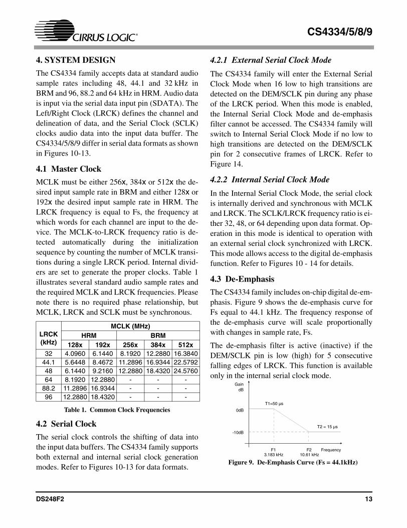
4. SYSTEM DESIGN
The CS4334 family accepts data at standard audiosample rates including 48, 44.1 and 32 kHz inBRM and 96, 88.2 and 64 kHz in HRM. Audio datais input via the serial data input pin (SDATA). TheLeft/Right Clock (LRCK) defines the channel anddelineation of data, and the Serial Clock (SCLK)clocks audio data into the input data buffer. TheCS4334/5/8/9 differ in serial data formats as shownin Figures 10-13.
4.1 Master Clock
MCLK must be either 256x, 384x or 512x the de-sired input sample rate in BRM and either 128x or192x the desired input sample rate in HRM. TheLRCK frequency is equal to Fs, the frequency atwhich words for each channel are input to the de-vice. The MCLK-to-LRCK frequency ratio is de-tected automatically during the initializationsequence by counting the number of MCLK transi-tions during a single LRCK period. Internal divid-ers are set to generate the proper clocks. Table 1illustrates several standard audio sample rates andthe required MCLK and LRCK frequencies. Pleasenote there is no required phase relationship, butMCLK, LRCK and SCLK must be synchronous.
Table 1. Common Clock Frequencies
4.2 Serial Clock
The serial clock controls the shifting of data intothe input data buffers. The CS4334 family supportsboth external and internal serial clock generationmodes. Refer to Figures 10-13 for data formats.
4.2.1 External Serial Clock Mode
The CS4334 family will enter the External SerialClock Mode when 16 low to high transitions aredetected on the DEM/SCLK pin during any phaseof the LRCK period. When this mode is enabled,the Internal Serial Clock Mode and de-emphasisfilter cannot be accessed. The CS4334 family willswitch to Internal Serial Clock Mode if no low tohigh transitions are detected on the DEM/SCLKpin for 2 consecutive frames of LRCK. Refer toFigure 14.
4.2.2 Internal Serial Clock Mode
In the Internal Serial Clock Mode, the serial clockis internally derived and synchronous with MCLKand LRCK. The SCLK/LRCK frequency ratio is ei-ther 32, 48, or 64 depending upon data format. Op-eration in this mode is identical to operation withan external serial clock synchronized with LRCK.This mode allows access to the digital de-emphasisfunction. Refer to Figures 10 - 14 for details.
4.3 De-Emphasis
The CS4334 family includes on-chip digital de-em-phasis. Figure 9 shows the de-emphasis curve forFs equal to 44.1 kHz. The frequency response ofthe de-emphasis curve will scale proportionallywith changes in sample rate, Fs.
The de-emphasis filter is active (inactive) if theDEM/SCLK pin is low (high) for 5 consecutivefalling edges of LRCK. This function is availableonly in the internal serial clock mode.
LRCK(kHz)
MCLK (MHz)HRM BRM
128x 192x 256x 384x 512x32 4.0960 6.1440 8.1920 12.2880 16.3840
44.1 5.6448 8.4672 11.2896 16.9344 22.579248 6.1440 9.2160 12.2880 18.4320 24.576064 8.1920 12.2880 - - -
88.2 11.2896 16.9344 - - -96 12.2880 18.4320 - - -
GaindB
-10dB
0dB
Frequency
T2 = 15 µs
T1=50 µs
F1 F23.183 kHz 10.61 kHz
Figure 9. De-Emphasis Curve (Fs = 44.1kHz)
DS248F2 13

CS4334/5/8/9
4.4 Initialization and Power-Down
The Initialization and Power-Down sequence flowchart is shown in Figure 14. The CS4334 family en-ters the Power-Down State upon initial power-up.The interpolation filters and delta-sigma modula-tors are reset, and the internal voltage reference,one-bit digital-to-analog converters and switched-capacitor low-pass filters are powered down. Thedevice will remain in the Power-Down mode untilMCLK and LRCK are present. Once MCLK andLRCK are detected, MCLK occurrences are count-ed over one LRCK period to determine theMCLK/LRCK frequency ratio. Power is then ap-plied to the internal voltage reference. Finally, pow-er is applied to the D/A converters and switched-capacitor filters, and the analog outputs will ramp tothe quiescent voltage, VQ.
4.5 Output Transient Control
The CS4334 family uses Popguard™ technology tominimize the effects of output transients duringpower-up and power-down. This technique elimi-nates the audio transients commonly produced bysingle-ended single-supply converters when it isimplemented with external DC-blocking capacitorsconnected in series with the audio outputs. Tomake best use of this feature, it is necessary to un-derstand its operation.
When the device is initially powered-up, the audiooutputs, AOUTL and AOUTR, are clamped toAGND. After a short delay of approximately 1000sample periods, each output begins to ramp to-wards its quiescent voltage, VQ. Approximately10,000 sample cycles later, the outputs reach VQand audio output begins. This gradual voltageramping allows time for the external DC-blockingcapacitor to charge to VQ, effectively blocking thequiescent DC voltage.
To prevent transients at power-down, the devicemust first enter its power-down state. This is ac-
complished by removing MCLK or LRCK. Whenthis occurs, audio output ceases and the internaloutput buffers are disconnected from AOUTL andAOUTR. A soft-start current sink is substituted inplace of AOUTL and AOUTR which allows theDC-blocking capacitors to slowly discharge. Oncethis charge is dissipated, the power to the devicemay be turned off, and the system is ready for thenext power-on.
To prevent an audio transient at the next power-on,the DC-blocking capacitors must fully dischargebefore turning off the power or exiting the power-down state. If full discharge does not occur, a tran-sient will occur when the audio outputs are initiallyclamped to AGND. The time that the device mustremain in the power-down state is related to thevalue of the DC-blocking capacitance. For exam-ple, with a 3.3 µF capacitor, the time that the devicemust remain in the power-down state will be ap-proximately 0.4 seconds.
4.6 Grounding and Power SupplyDecoupling
As with any high resolution converter, the CS4334family requires careful attention to power supplyand grounding arrangements to optimize perfor-mance. Figure 7 shows the recommended power ar-rangement with VA connected to a clean +5Vsupply. For best performance, decoupling capaci-tors should be located as close to the device pack-age as possible with the smallest capacitor closest.
4.7 Analog Output and Filtering
The analog filter present in the CS4334 family is aswitched-capacitor filter followed by a continuoustime low pass filter. Its response, combined withthat of the digital interpolator, is given in Figures15 - 22.
14 DS248F2

CS4334/5/8/9
LR C K
S C LK
Left C hanne l R igh t C hannel
SD A T A +3 +2 +1 LS B+5 +4M SB -1 -2 -3 -4 -5 +3 +2 +1 LS B+5 +4M S B -1 -2 -3 -4
Internal SCLK Mode External SCLK Mode
I2S, 16-Bit data and INT SCLK = 32 Fs ifMCLK/LRCK = 512, 256 or 128I2S, Up to 24-Bit data and INT SCLK = 48 Fs ifMCLK/LRCK = 384 or 192
I2S, up to 24-Bit DataData Valid on Rising Edge of SCLK
Figure 10. CS4334 Data Format (I2S)
LR C K
S C LK
Left C hanne l R igh t C hannel
SD A T A +3 +2 +1 LS B+5 +4M SB -1 -2 -3 -4 -5 +3 +2 +1 LS B+5 +4M S B -1 -2 -3 -4
Internal SCLK Mode External SCLK Mode
Left Justified, up to 24-Bit DataINT SCLK = 64 Fs if MCLK/LRCK = 512, 256 or 128INT SCLK = 48 Fs if MCLK/LRCK = 384 or 192
Left Justified, up to 24-Bit DataData Valid on Rising Edge of SCLK
Figure 11. CS4335 Data Format
LR C K
S C LK
Le ft Channel R igh t C hannel
SD A TA 6 5 4 3 2 1 09 8 715 14 13 12 11 10 6 5 4 3 2 1 09 8 715 14 13 12 11 10
32 clocks
Internal SCLK Mode External SCLK Mode
Right Justified, 16-Bit DataINT SCLK = 32 Fs if MCLK/LRCK = 512, 256 or 128INT SCLK = 48 Fs if MCLK/LRCK = 384 or 192
Right Justified, 16-Bit DataData Valid on Rising Edge of SCLKSCLK Must Have at Least 32 Cycles per LRCK Period
Figure 12. CS4338 Data Format
DS248F2 15

CS4334/5/8/9
LR CK
S C LK
Le ft C hannel R igh t C hannel
S DA TA 6 5 4 3 2 1 09 8 715 14 13 12 11 101 0 6 5 4 3 2 1 09 8 715 14 13 12 11 1017 16 17 16
32 clocks
Internal SCLK Mode External SCLK Mode
Right Justified, 18-Bit DataINT SCLK = 64 Fs if MCLK/LRCK = 512, 256 or 128INT SCLK = 48 Fs if MCLK/LRCK = 384 or 192
Right Justified, 18-Bit DataData Valid on Rising Edge of SCLKSCLK Must Have at Least 36 Cycles per LRCK Period
Figure 13. CS4339 Data Format
16 DS248F2

CS4334/5/8/9
Figure 14. CS4334/5/8/9 Initialization and Power-Down Sequence
DS248F2 17

CS4334/5/8/9
4.8 Overall Base-Rate Frequency Response
Figure 15. Stopband Rejection Figure 16. Transition Band
Figure 17. Transition Band Figure 18. Passband Ripple
18 DS248F2

CS4334/5/8/9
4.9 Overall High-Rate Frequency Response
Figure 19. Stopband Rejection Figure 20. Transition Band
Figure 21. Transition Band Figure 22. Passband Ripple
DS248F2 19

CS4334/5/8/9
4.10 Base Rate Mode Performance Plots
-140
+0
-130
-120
-110
-100
-90
-80
-70
-60
-50
-40
-30
-20
-10
dBr
A
2k 20k4k 6k 8k 10k 12k 14k 16k 18k
Hz2k 4k 6k 8k 10k 12k 14k 16k 18k
-140
-130
-120
-110
-100
-90
-80
-70
-60
-50
-40
-30
-20
-10
+0
dBr
A
Hz
20k
+0-10
-20
-30
-40
-50
-60
-70
-80
-90
-100
-110
-120-130
-140
dBr
A
2k 6k4k 8k 10k 12k 14k 16k 18k 20kHz
-140
+0
-130
-120
-110
-100
-90
-80
-70
-60
-50
-40
-30
-20
-10
dBr
A
2k 20k4k 6k 8k 10k 12k 14k 16k 18k
Hz 20k2k 4k 6k 8k 10k 12k 14k 16k 18k
-140
-130
-120
-110
-100
-90
-80
-70
-60
-50
-40
-30
-20
-10
+0
dBr
A
Hz
20k2k 6k4k 8k 10k 12k 14k 16k 18k 20kHz
+0-10
-20
-30
-40
-50
-60
-70
-80
-90
-100
-110
-120-130
-140
dBr
A
(16k FFT of a 1 kHz input signal)
Figure 23. 0 dBFS FFT (BRM)
(16k FFT of a 1 kHz input signal)
Figure 24. -60 dBFS FFT (BRM)
-140
+0
-130
-120
-110
-100
-90
-80
-70
-60
-50
-40
-30
-20
-10
dBr
A
2k 20k4k 6k 8k 10k 12k 14k 16k 18k
Hz2k 4k 6k 8k 10k 12k 14k 16k 18k
-140
-130
-120
-110
-100
-90
-80
-70
-60
-50
-40
-30
-20
-10
+0
dBr
A
Hz
20k
+0-10
-20
-30
-40
-50
-60
-70
-80
-90
-100
-110
-120-130
-140
dBr
A
2k 6k4k 8k 10k 12k 14k 16k 18k 20kHz
-140
+ 0
-130
-120
-110
-100
-90
-80
-70
-60
-50
-40
-30
-20
-10
dBr
A
2k 20k4k 6k 8k 10k 12k 14k 16k 18k
Hz2k 4k 6k 8k 10k 12k 14k 16k 18k
-140
-130
-120
-110
-100
-90
-80
-70
-60
-50
-40
-30
-20
-10
+0
dBr
A
Hz
20k
+0
-10
-20
-30
-40
-50
-60
-70
-80
-90
-100
-110
-120
-130
-140
dBr
A
2k 6k4k 8k 10k 12k 14k 16k 18k 20kHz
(16k FFT with no input signal)
Figure 25. Idle Channel Noise FFT (BRM)
(16k FFT of intermodulation distortion using 13 kHz and 14 kHz input signals)
Figure 26. Twin Tone IMD FFT (BRM)
-110
-60
-100
-90
-80
-70
dBr
A
-60 +0-50 -40 -30 -20 -10
dBFS
-50 -40 -30 -20 -10
dBFS
-60 +0-110
-100
-90
-80
-70
-60
dBr
A
-110
+0
-100
-90
-80
-70
-60
-50
-40
-30
-20
-10
dBr
A
20 20k50 100 200 500 1k 2k 5k 10k
Hz
-110
-100
-90
-80
-70
-60
-50
-40
-30
-20
-10
+0
dBr
A
20 50 100 200 500 1k 2k 5k 10k 20kHz
+0
-10
-20
-30
-40
-50
-60
-70
-80
-90
-100
-110
dBr
A
10050 200 500 1k 2k 5k 10kHz
20 20k
(THD+N plots measured using a 1kHz 24-bit dithered input signal)
Figure 27. THD+N vs. Amplitude (BRM)
(THD+N plots measured using a 1kHz 24-bit dithered input signal)
Figure 28. THD+N vs. Frequency (BRM)
All measurements were taken from the CDB4334 evaluation board using the Audio Precision Dual DomainSystem Two Cascade.
20 DS248F2

CS4334/5/8/9
4.11 High Rate Mode Performance Plots
-140
+0
-130
-120
-110
-100
-90
-80
-70
-60
-50
-40
-30
-20
-10
dBr
A
2k 20k4k 6k 8k 10k 12k 14k 16k 18k
Hz2k 4k 6k 8k 10k 12k 14k 16k 18k
-140
-130
-120
-110
-100
-90
-80
-70
-60
-50
-40
-30
-20
-10
+0
dBr
A
Hz
20k
+0-10
-20
-30
-40
-50
-60
-70
-80
-90
-100
-110
-120-130
-140
dBr
A
2k 6k4k 8k 10k 12k 14k 16k 18k 20kHz
-140
+ 0
-130
-120
-110
-100
-90
-80
-70
-60
-50
-40
-30
-20
-10
dBr
A
2k 20k4k 6k 8k 10k 12k 14k 16k 18k
Hz2k 4k 6k 8k 10k 12k 14k 16k 18k
-140
-130
-120
-110
-100
-90
-80
-70
-60
-50
-40
-30
-20
-10
+0
dBr
A
Hz
20k
+0-10
-20
-30
-40-50
-60
-70
-80-90
-100
-110
-120-130
-140
dBr
A
2k 6k4k 8k 10k 12k 14k 16k 18k 20kHz
(16k FFT of a 1 kHz input signal)
Figure 29. 0 dBFS FFT (HRM)
(16k FFT of a 1 kHz input signal)
Figure 30. -60 dBFS FFT (HRM)
-140
+0
-130
-120
-110
-100
-90
-80
-70
-60
-50
-40
-30
-20
-10
dBr
A
2k 20k4k 6k 8k 10k 12k 14k 16k 18k
Hz2k 4k 6k 8k 10k 12k 14k 16k 18k
-140
-130
-120
-110
-100
-90
-80
-70
-60
-50
-40
-30
-20
-10
+0
dBr
A
Hz
20k
+0-10
-20
-30
-40
-50
-60
-70
-80
-90
-100
-110
-120-130
-140
dBr
A
2k 6k4k 8k 10k 12k 14k 16k 18k 20kHz
Audio Precis ion 08/05/99 11:11:36D-A CCIF IMD vs AMPLITUDE
-140
+ 0
-130
-120
-110
-100
-90
-80
-70
-60
-50
-40
-30
-20
-10
dBr
A
2k 20k4k 6k 8k 10k 12k 14k 16k 18k
Hz
2k 4k 6k 8k 10k 12k 14k 16k 18k-140
-130
-120
-110
-100
-90
-80
-70
-60
-50
-40
-30
-20
-10
+0
dBr
A
Hz
20k
+0-10
-20
-30
-40
-50
-60
-70
-80
-90
-100
-110
-120
-130
-140
dBr
A
2k 6k4k 8k 10k 12k 14k 16k 18k 20kHz
(16k FFT with no input signal)
Figure 31. Idle Channel Noise FFT (HRM)
(16k FFT of intermodulation distortion using 13 kHz and 14 kHz input signals)
Figure 32. Twin Tone IMD FFT (HRM)
-110
-60
-100
-90
-80
-70
dBr
A
-60 +0-50 -40 -30 -20 -10
dBFS-50 -40 -30 -20 -10
dBFS
-60 +0-110
-100
-90
-80
-70
-60
dBr
A
-110
+0
-100
-90
-80
-70
-60
-50
-40
-30
-20
-10
dBr
A
20 20k50 100 200 500 1k 2k 5k 10k
Hz
-110
-100
-90
-80
-70
-60
-50
-40
-30
-20
-10
+0
dBr
A
20 50 100 200 500 1k 2k 5k 10k 20kHz
10050 200 500 1k 2k 5k 10kHz
20 20k
+0
-10
-20
-30
-40
-50
-60
-70
-80
-90
-100
-110
dBr
A
(THD+N plots measured using a 1kHz 24-bit dithered input signal)
Figure 33. THD+N vs. Amplitude (HRM)
(THD+N plots measured using a 1kHz 24-bit dithered input signal)
Figure 34. THD+N vs. Frequency (HRM)
All measurements were taken from the CDB4334 evaluation board using the Audio Precision Dual DomainSystem Two Cascade.
DS248F2 21
CS4334/5/8/9
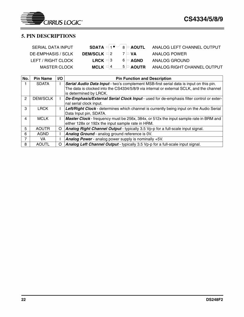
5. PIN DESCRIPTIONS
No. Pin Name I/O Pin Function and Description1 SDATA I Serial Audio Data Input - two’s complement MSB-first serial data is input on this pin.
The data is clocked into the CS4334/5/8/9 via internal or external SCLK, and the channelis determined by LRCK.
2 DEM/SCLK I De-Emphasis/External Serial Clock Input - used for de-emphasis filter control or exter-nal serial clock input.
3 LRCK I Left/Right Clock - determines which channel is currently being input on the Audio SerialData Input pin, SDATA.
4 MCLK I Master Clock - frequency must be 256x, 384x, or 512x the input sample rate in BRM andeither 128x or 192x the input sample rate in HRM.
5 AOUTR O Analog Right Channel Output - typically 3.5 Vp-p for a full-scale input signal.6 AGND I Analog Ground - analog ground reference is 0V.7 VA I Analog Power - analog power supply is nominally +5V.8 AOUTL O Analog Left Channel Output - typically 3.5 Vp-p for a full-scale input signal.
SERIAL DATA INPUT SDATA AOUTL ANALOG LEFT CHANNEL OUTPUT
DE-EMPHASIS / SCLK DEM/SCLK VA ANALOG POWER
LEFT / RIGHT CLOCK LRCK AGND ANALOG GROUND
MASTER CLOCK MCLK AOUTR ANALOG RIGHT CHANNEL OUTPUT
72
63
54
81
22 DS248F2

CS4334/5/8/9
6. PARAMETER DEFINITIONS
Total Harmonic Distortion + Noise (THD+N)- The ratio of the rms value of the signal to therms sum of all other spectral components over the specified bandwidth (typically 10Hz to20kHz), including distortion components. Expressed in decibels.
Dynamic Range - The ratio of the full scale rms value of the signal to the rms sum of all otherspectral components over the specified bandwidth. Dynamic range is a signal-to-noisemeasurement over the specified bandwidth made with a -60 dBFS signal. 60 dB is then addedto the resulting measurement to refer the measurement to full scale. This technique ensures thatthe distortion components are below the noise level and do not effect the measurement. Thismeasurement technique has been accepted by the Audio Engineering Society, AES17-1991, andthe Electronic Industries Association of Japan, EIAJ CP-307.
Interchannel Isolation - A measure of crosstalk between the left and right channels. Measuredfor each channel at the converter's output with all zeros to the input under test and a full-scalesignal applied to the other channel. Units in decibels.
Interchannel Gain Mismatch - The gain difference between left and right channels. Units indecibels.
Gain Error - The deviation from the nominal full scale analog output for a full scale digitalinput.
Gain Drift - The change in gain value with temperature. Units in ppm/°C.
7. REFERENCES
1) "How to Achieve Optimum Performance from Delta-Sigma A/D & D/A Converters" by Steven Harris.Paper presented at the 93rd Convention of the Audio Engineering Society, October 1992.
2) CDB4334/5/8/9 Evaluation Board Datasheet
DS248F2 23

CS4334/5/8/9
8. ORDER INFORMATION:
9. FUNCTIONAL COMPATIBILITY
CS4330-KS ⇒ CS4339-KS
CS4331-KS ⇒ CS4334-KS
CS4333-KS ⇒ CS4338-KS
CS4330-BS ⇒ CS4339-BS/-DS
CS4331-BS ⇒ CS4334-BS/-DS
CS4333-BS ⇒ CS4338-BS/-DS
Model Temperature Package Serial InterfaceCS4334-KS -10 to +70 °C 8-pin Plastic SOIC 16 to 24-bit, I2SCS4335-KS -10 to +70 °C 8-pin Plastic SOIC 16 to 24-bit, left justifiedCS4338-KS -10 to +70 °C 8-pin Plastic SOIC 16-bit, right justifiedCS4339-KS -10 to +70 °C 8-pin Plastic SOIC 18-bit, right justified, 32 Fs Internal SCLK modeCS4334-BS -40 to +85 °C 8-pin Plastic SOIC 16 to 24-bit, I2SCS4335-BS -40 to +85 °C 8-pin Plastic SOIC 16 to 24-bit, left justifiedCS4338-BS -40 to +85 °C 8-pin Plastic SOIC 16-bit, right justifiedCS4339-BS -40 to +85 °C 8-pin Plastic SOIC 18-bit, right justified, 32 Fs Internal SCLK modeCS4334-DS -40 to +85 °C 8-pin Plastic SOIC 16 to 24-bit, I2SCS4335-DS -40 to +85 °C 8-pin Plastic SOIC 16 to 24-bit, left justifiedCS4338-DS -40 to +85 °C 8-pin Plastic SOIC 16-bit, right justifiedCS4339-DS -40 to +85 °C 8-pin Plastic SOIC 18-bit, right justified, 32 Fs Internal SCLK mode
24 DS248F2

CS4334/5/8/9
10. PACKAGE DIMENSIONS
INCHES MILLIMETERSDIM MIN MAX MIN MAX
A 0.053 0.069 1.35 1.75A1 0.004 0.010 0.10 0.25B 0.013 0.020 0.33 0.51C 0.007 0.010 0.19 0.25D 0.189 0.197 4.80 5.00E 0.150 0.157 3.80 4.00e 0.040 0.060 1.02 1.52H 0.228 0.244 5.80 6.20L 0.016 0.050 0.40 1.27∝ 0° 8° 0° 8°
JEDEC # : MS-012
8L SOIC (150 MIL BODY) PACKAGE DRAWING
D
HE
e
b
A1
A
c
L
∝SEATINGPLANE
1
DS248F2 25