Embed Size (px)
Citation preview

Si5332 Reference Manual
The Si5332 is a high-performance, low-jitter clock generator capable of synthesizing fiveindependent banks of user-programmable clock frequencies up to 333.33 MHz, whileproviding up to 12 differential or 24 single-ended output clocks. The Si5332 supportsfree run operation using an external crystal, or optional internal crystal, as well as lock toan external clock signal. The output drivers are configurable to support common signalformats, such as LVPECL, LVDS, HCSL, and LVCMOS. Separate output supply pinsallow supply voltages of 3.3, 2.5, 1.8 V and 1.5V (CMOS only) to power the multi-formatoutput drivers. The core voltage supply (VDD) accepts 3.3, 2.5, or 1.8 V and is inde-pendent from the output supplies (VDDOs). Using its two-stage synthesis architectureand patented high-resolution Multisynth technology, the Si5332 can generate three fullyindependent / non-harmonically-related bank frequencies from a single input frequency.
÷ P PFD LF
÷Mn/Md
÷R
÷R
÷R
÷R
÷R
÷R
÷R
÷R
÷R
÷R
÷R
÷R
÷N0
÷N1
÷O0
÷O1
÷O2
÷O3
÷O4
1-31
10-255
10-50 MHz 2.375-2.625 GHz
10-255
8-255
10-250 MHz
10-250 MHz
10-312.5 MHz
10-312.5 MHz
10-312.5 MHz
10-312.5 MHz
10-312.5 MHz
1-63
10-50 MHz
10-250 MHz
10-250 MHz
10-250 MHz
10-30 MHz
VDD_XTAL
VDDA
VDDOA
VDDOB
VDDOC
VDDOD
VDDOE
XA/CLKIN_1
XB
CLKIN_2
nCLKIN_2
CLKIN_3
nCLKIN_3
OUT0
OUT1
OUT2
OUT3
OUT4
OUT5
OUT6
OUT7
OUT8
OUT9
OUT10
OUT11
KEY FEATURES
• Any-Frequency 6/8/12-outputprogrammable clock generators
• Offered in three different package sizes,supporting different combinations of out-put clocks and user configurable hardwareinput pins• 32-pin QFN/LGA, up to 6 outputs• 40-pin QFN/LGA, up to 8 outputs• 48-pin QFN/LGA, up to 12 outputs
• Multisynth technology enables anyfrequency synthesis on any output up to250 MHz
• Highly configurable output path featuring across point mux
• Up to three independent fractionalsynthesis output paths
• Up to five independent integer dividers• Down and center spread spectrum• Embedded 50 MHz crystal option• Input frequency range:
• External crystal: 16 to 50 MHz• Embedded crystal: 50 MHz• Differential clock: 10 to 250 MHz• LVCMOS clock: 10 to 170 MHz
• Output frequency range:• Differential: 5 to 312.5 MHz• LVCMOS: 5 to 170 MHz
• User-configurable clock output signalformat per output: LVDS, LVPECL, HCSL,LVCMOS
• Easy device configuration using ourClockBuilder Pro™ (CBPro) software toolavailable for download from our web site
• Temperature range: –40 to +85 °C (Lgrade: +25 C to +85 C)
• Pb-free, RoHS-6 compliant• For more information, refer to the Si5332
data sheet
Skyworks Solutions, Inc. • Phone [781] 376-3000 • Fax [781] 376-3100 • [email protected] • www.skyworksinc.com1 Rev. 0.6 • Skyworks Proprietary Information • Products and Product Information are Subject to Change Without Notice • February 15, 2022 1
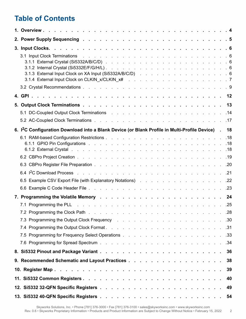
Table of Contents1. Overview . . . . . . . . . . . . . . . . . . . . . . . . . . . . . . . . . 4
2. Power Supply Sequencing . . . . . . . . . . . . . . . . . . . . . . . . . . 5
3. Input Clocks. . . . . . . . . . . . . . . . . . . . . . . . . . . . . . . . 63.1 Input Clock Terminations . . . . . . . . . . . . . . . . . . . . . . . . . . 6
3.1.1 External Crystal (Si5332A/B/C/D) . . . . . . . . . . . . . . . . . . . . . . 63.1.2 Internal Crystal (Si5332E/F/G/H/L) . . . . . . . . . . . . . . . . . . . . . . 63.1.3 External Input Clock on XA Input (Si5332A/B/C/D) . . . . . . . . . . . . . . . . 63.1.4 External Input Clock on CLKIN_x/CLKIN_x# . . . . . . . . . . . . . . . . . . 7
3.2 Crystal Recommendations . . . . . . . . . . . . . . . . . . . . . . . . . . 9
4. GPI . . . . . . . . . . . . . . . . . . . . . . . . . . . . . . . . . . 12
5. Output Clock Terminations . . . . . . . . . . . . . . . . . . . . . . . . . 135.1 DC-Coupled Output Clock Terminations . . . . . . . . . . . . . . . . . . . . .14
5.2 AC-Coupled Clock Terminations . . . . . . . . . . . . . . . . . . . . . . . .17
6. I2C Configuration Download into a Blank Device (or Blank Profile in Multi-Profile Device) . 186.1 RAM-based Configuration Restrictions . . . . . . . . . . . . . . . . . . . . . .18
6.1.1 GPIO Pin Configurations . . . . . . . . . . . . . . . . . . . . . . . . .186.1.2 External Crystal . . . . . . . . . . . . . . . . . . . . . . . . . . . .18
6.2 CBPro Project Creation . . . . . . . . . . . . . . . . . . . . . . . . . . .19
6.3 CBPro Register File Preparation . . . . . . . . . . . . . . . . . . . . . . . .20
6.4 I2C Download Process . . . . . . . . . . . . . . . . . . . . . . . . . . .21
6.5 Example CSV Export File (with Explanatory Notations) . . . . . . . . . . . . . . . .22
6.6 Example C Code Header File . . . . . . . . . . . . . . . . . . . . . . . . .23
7. Programming the Volatile Memory . . . . . . . . . . . . . . . . . . . . . . 247.1 Programming the PLL . . . . . . . . . . . . . . . . . . . . . . . . . . .25
7.2 Programming the Clock Path . . . . . . . . . . . . . . . . . . . . . . . . .28
7.3 Programming the Output Clock Frequency . . . . . . . . . . . . . . . . . . . .30
7.4 Programming the Output Clock Format . . . . . . . . . . . . . . . . . . . . . .31
7.5 Programming for Frequency Select Operations . . . . . . . . . . . . . . . . . . .33
7.6 Programming for Spread Spectrum . . . . . . . . . . . . . . . . . . . . . . .34
8. Si5332 Pinout and Package Variant . . . . . . . . . . . . . . . . . . . . . . 36
9. Recommended Schematic and Layout Practices . . . . . . . . . . . . . . . . . 38
10. Register Map . . . . . . . . . . . . . . . . . . . . . . . . . . . . . . 39
11. Si5332 Common Registers . . . . . . . . . . . . . . . . . . . . . . . . . 40
12. Si5332 32-QFN Specific Registers . . . . . . . . . . . . . . . . . . . . . . 49
13. Si5332 40-QFN Specific Registers . . . . . . . . . . . . . . . . . . . . . . 54
Skyworks Solutions, Inc. • Phone [781] 376-3000 • Fax [781] 376-3100 • [email protected] • www.skyworksinc.com2 Rev. 0.6 • Skyworks Proprietary Information • Products and Product Information are Subject to Change Without Notice • February 15, 2022 2

14. Si5332 48-QFN Specific Registers . . . . . . . . . . . . . . . . . . . . . . 60
Skyworks Solutions, Inc. • Phone [781] 376-3000 • Fax [781] 376-3100 • [email protected] • www.skyworksinc.com3 Rev. 0.6 • Skyworks Proprietary Information • Products and Product Information are Subject to Change Without Notice • February 15, 2022 3

1. Overview
In addition to clock generation, the input clocks can bypass the synthesis stage enabling the Si5332 to be used as a high-performanceclock buffer or a combination of a buffer and generator. The Multisynth dividers have two sets of divide ratio registers, an A set and aB set. The active in-use divide ratio can be switched between the A set or B set via external input pin or register control. This featureallows for dynamic frequency shifting at ppb accuracy for applications such as frequency margining. Similar A set and B set dividerratios are available for the integer dividers, but the ratios must be integer related. CBPro supports use of A and B divider sets. Spreadspectrum is available for any clock output from two Multisynth dividers for use in EMI-sensitive applications, such as PCI Express.Configurations and controls of the Si5332 are mainly handled through I2C. Any GPI pin can be programmed to be clock input select,frequency A/B select, spread enable, output enable, or I2C address select.
Si5332 Reference Manual • Overview
Skyworks Solutions, Inc. • Phone [781] 376-3000 • Fax [781] 376-3100 • [email protected] • www.skyworksinc.com4 Rev. 0.6 • Skyworks Proprietary Information • Products and Product Information are Subject to Change Without Notice • February 15, 2022 4

2. Power Supply Sequencing
The Si5332 VDD_core voltages are VDD_DIG, VDD_XTAL and VDDA. These 3 VDD_core pins must all use the *same* voltage.Power supply sequencing between VDD_core and any VDDOx pin is allowed in any order. However, to minimize the “bring up” time,it is recommended that VDD_core is powered up first, this ensures that the NVM download is completed first. The register bit field“VDD_XTAL_OK” is set to indicate input buffer(s) and crystal oscillator are powered up. Once the appropriate VDDOx supplies arepowered-up, the VDDO_OK register field will indicate output driver bank supply voltage status. These status registers are availableto provide an indication of general device status and presence of output driver voltages. The figure below shows the Si5332 devicepower-up sequencing and expected device behavior. Note that a blank (unconfigured) part will stop and wait to be configured withoutputs disabled.
Power supplies for VDDA, VDD_DIG, VDD_XTAL
stable
Time (system time delay) for NVM download
Is this a blank part?
Yes
No
Time (system time delay) for Oscillator startup/ Time
(system time delay) for input clock availability
Time (system time delay) for PLL lock
Outputs available and stable
Program Si5332 volatile memory with a frequency
plan
Figure 2.1. Power Supply Sequencing for Si5332
Si5332 Reference Manual • Power Supply Sequencing
Skyworks Solutions, Inc. • Phone [781] 376-3000 • Fax [781] 376-3100 • [email protected] • www.skyworksinc.com5 Rev. 0.6 • Skyworks Proprietary Information • Products and Product Information are Subject to Change Without Notice • February 15, 2022 5

3. Input Clocks
The Si5332 has three input clock nodes, the XA/XB pair, the CLKIN_2/CLKIN_2# pair and the CLKIN_3/CLKIN_3# pair.
XA/XB supports a crystal input or an external clock input whereas the CLKIN_x/CLKIN_x# pairs support ONLY external clock inputs.The GPI pins can be set to select the active input clock for the PLL (or the user can set the active input via register writes).
3.1 Input Clock Terminations
Supported input clock sources for the Si5332 are:1. External crystal attached to the Si5332 XA/XB inputs (Si5332A/B/C/D only).2. Internal crystal (Si5332E/F/G/H/L only).3. External single-ended clock attached to XA (Si5332A/B/C/D only).4. Externally supplied clock attached to available CLKIN_x/CLKINx# inputs.
3.1.1 External Crystal (Si5332A/B/C/D)
An external crystal can be connected to a Si5332A/B/C/D device’s XA/XB inputs as shown below. See section 3.2 for a list ofrecommended crystals, or see Table 5.4 in the Si5332 datasheet for crystal specifications when selecting a different crystal. Note theexternal crystal specifications in Si5332 datasheet Table 5.4 must be met.
XA
XB
Si5332
InternalOsc
Figure 3.1. External Crystal Connection
3.1.2 Internal Crystal (Si5332E/F/G/H/L)
An internal crystal option is available by selecting the E, F, G, H, or L variant of the Si5332. The internal crystal is a fixed 50 MHzcrystal. No external crystal or other components should be connected to the XA/XB pins and the pins should not have signals routednext to or underneath. For layout purposes, the XA/XB pins should be treated as if the crystal is attached.
3.1.3 External Input Clock on XA Input (Si5332A/B/C/D)
The XA input can accept an externally supplied, AC coupled clock with maximum voltage swing of 1Vpp. See figure below forconnection details. The XB pin must be left open with nothing connected. If using this input clock mode, it is suggested to zero-out theinternal crystal loading capacitance (CL) for best operation.
0.1 µFXA
XB
Si5332
Form
at*
Term
inat
ion
Driver
ControlledImpedance
NoConnect
XA input max swing = 1 Vpp
InternalOsc
Figure 3.2. External Input Clock on XA Input
Si5332 Reference Manual • Input Clocks
Skyworks Solutions, Inc. • Phone [781] 376-3000 • Fax [781] 376-3100 • [email protected] • www.skyworksinc.com6 Rev. 0.6 • Skyworks Proprietary Information • Products and Product Information are Subject to Change Without Notice • February 15, 2022 6
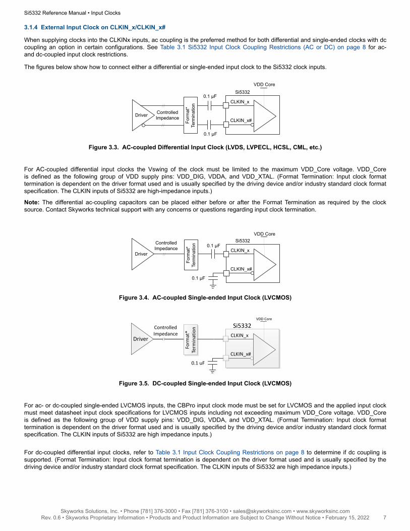
3.1.4 External Input Clock on CLKIN_x/CLKIN_x#
When supplying clocks into the CLKINx inputs, ac coupling is the preferred method for both differential and single-ended clocks with dccoupling an option in certain configurations. See Table 3.1 Si5332 Input Clock Coupling Restrictions (AC or DC) on page 8 for ac-and dc-coupled input clock restrictions.
The figures below show how to connect either a differential or single-ended input clock to the Si5332 clock inputs.
0.1 µF
0.1 µFCLKIN_x
CLKIN_x#
Si5332VDD Core
Form
at*
Term
inat
ion
Driver ControlledImpedance
Figure 3.3. AC-coupled Differential Input Clock (LVDS, LVPECL, HCSL, CML, etc.)
For AC-coupled differential input clocks the Vswing of the clock must be limited to the maximum VDD_Core voltage. VDD_Coreis defined as the following group of VDD supply pins: VDD_DIG, VDDA, and VDD_XTAL. (Format Termination: Input clock formattermination is dependent on the driver format used and is usually specified by the driving device and/or industry standard clock formatspecification. The CLKIN inputs of Si5332 are high-impedance inputs.)
Note: The differential ac-coupling capacitors can be placed either before or after the Format Termination as required by the clocksource. Contact Skyworks technical support with any concerns or questions regarding input clock termination.
0.1 µF
0.1 µFCLKIN_x
CLKIN_x#
Si5332VDD Core
Form
at*
Term
inat
ion
Driver
ControlledImpedance
Figure 3.4. AC-coupled Single-ended Input Clock (LVCMOS)
0.1 uF
CLKIN_x
CLKIN_x#
Si5332VDD Core
Form
at*
Term
inat
ion
Driver
ControlledImpedance
Figure 3.5. DC-coupled Single-ended Input Clock (LVCMOS)
For ac- or dc-coupled single-ended LVCMOS inputs, the CBPro input clock mode must be set for LVCMOS and the applied input clockmust meet datasheet input clock specifications for LVCMOS inputs including not exceeding maximum VDD_Core voltage. VDD_Coreis defined as the following group of VDD supply pins: VDD_DIG, VDDA, and VDD_XTAL. (Format Termination: Input clock formattermination is dependent on the driver format used and is usually specified by the driving device and/or industry standard clock formatspecification. The CLKIN inputs of Si5332 are high impedance inputs.)
For dc-coupled differential input clocks, refer to Table 3.1 Input Clock Coupling Restrictions on page 8 to determine if dc coupling issupported. (Format Termination: Input clock format termination is dependent on the driver format used and is usually specified by thedriving device and/or industry standard clock format specification. The CLKIN inputs of Si5332 are high impedance inputs.)
Si5332 Reference Manual • Input Clocks
Skyworks Solutions, Inc. • Phone [781] 376-3000 • Fax [781] 376-3100 • [email protected] • www.skyworksinc.com7 Rev. 0.6 • Skyworks Proprietary Information • Products and Product Information are Subject to Change Without Notice • February 15, 2022 7

Table 3.1. Si5332 Input Clock Coupling Restrictions (AC or DC)
Format VDD_Core
3.3 V 2.5 V 1.8 V
LVDS 3.3 V/2.5 V AC or DC AC only AC only
LVDS 1.8 V AC or DC AC only AC only
LVPECL 3.3 V/2.5 V AC or DC AC only AC only
HCSL AC or DC AC or DC AC only
CML AC only AC only AC only
LVCMOS AC or DC AC or DC AC or DC
Note:
1. For dc-coupled, input clock peak voltage must not exceed VDD_Core and minimum voltage must not be below GND.2. For ac-coupled, peak swing must not exceed VDD_Core.
Si5332 Reference Manual • Input Clocks
Skyworks Solutions, Inc. • Phone [781] 376-3000 • Fax [781] 376-3100 • [email protected] • www.skyworksinc.com8 Rev. 0.6 • Skyworks Proprietary Information • Products and Product Information are Subject to Change Without Notice • February 15, 2022 8

3.2 Crystal Recommendations
The crystals in the table below are recommended for use with Si5332. The crystals listed are 25 and 27 MHz frequencies. However,when choosing any crystal frequency between 16-30 MHz, a crystal with with ESR less than (or equal to) 50 Ω and CL less than (orequal to) 20 pF can be used with Si5332. When choosing crystals of 31-50 MHz frequencies, C0 should not exceed 2 pF, CL should notexceed 10 pF and the ESR should not exceed 50 Ω.
Table 3.2. Recommended Crystals
Crystal Part Number Make Stability CL ESR
ECS-25-18-30B-AKN ECS 30ppm 18pf 30 Ω
ECS-27-18-30B-AKN 30ppm 18pf 30 Ω
FOXSDLF/250FR-20 Fox 30ppm 20pf 30 Ω
FA-238V-25.000000MHz12.0+15.0-15.0 Epson 50ppm 12pf 50 Ω
ABM3B-25.000MHz-18-50-D1U Abracon 20ppm 18pf 50 Ω
ABM3B-27.000MHz-18-50-D1U 20ppm 18pf 50 Ω
ABM3B-25.000MHz-18-60-D1U 30ppm 18pf 60 Ω
ABM3B-27.000MHz-18-60-D1U 30ppm 18pf 60 Ω
ABM3B-25.000MHz-12-50-D1U 10ppm 10pf 50 Ω
ABM3B-27.000MHz-12-50-D1U 10ppm 10pf 50 Ω
AA-25.000MALE-T TXC 30ppm 12pf 50 Ω
AA-27.000MAGK-T 30ppm 20pf 50 Ω
FQ5032B-25.000 Fox 30ppm 20pf 50 Ω
FQ5032B-27.000
NX5032GA-25.000M-STD-CSK-4 NDK 30ppm 8pf 50 Ω
NX5032GA-25.000000MHZ-LN-CD-1 30ppm 8pf 70 Ω
NX5032GA-27M-STD-CSK-4 30ppm 8pf 50 Ω
NX5032GA-27.000000MHZ-LN-CD-1 30ppm 8pf 70 Ω
7A-25.000MAAE TXC 30ppm 12pf 50 Ω
7A-25.000MAAJ 30ppm 18pf 50 Ω
7A-27.000MAAE 30ppm 12pf 50 Ω
7A-27.000MAAJ 30ppm 18pf 50 Ω
Si5332 Reference Manual • Input Clocks
Skyworks Solutions, Inc. • Phone [781] 376-3000 • Fax [781] 376-3100 • [email protected] • www.skyworksinc.com9 Rev. 0.6 • Skyworks Proprietary Information • Products and Product Information are Subject to Change Without Notice • February 15, 2022 9

Crystals will resonate at their specified frequency (i.e., be “on-frequency”) if the capacitive loading across the crystal’s terminals is thesame as specified by the crystal loading capacitance (CL) specification. The total loading capacitance presented to the crystal mustfactor in all capacitance sources such as parasitic “stray” capacitance as well as added loading capacitance. Stray capacitance comesfrom sources like PCB traces, capacitive coupling to nearby components, as well as any stray capacitance within the oscillator deviceitself. For “on-frequency” oscillator operation, all capacitance sources must be considered to determine the correct total capacitancepresented to the crystal to match it’s required CL.
The Si5332 contains variable internal loading capacitors (CLVAR) to provide any necessary added crystal matching capacitance soexternal matching capacitors are not needed. The figure below shows the Si5332’s internal variable capacitance and the two sources ofstray loading capacitance.
Si5332
InternalOsc
External Stray Capacitance CLSEXT
Internal Variable Capacitance CLVAR
Internal Stray Capacitance CLSINT
Cry
stal
XA
XB
Figure 3.6. Sources of Crystal Loading Capacitance
Using the Si5332’s internal variable loading capacitors (CLVAR), the crystal’s required CL can be matched by adding capacitance to theexternal stray and internal device capacitance. The total stray capacitance must be less than the required crystal loading capacitanceCL. A value for CLVAR must be selected such that:
Crystal CL = CLVAR + CLSINT + CLSEXT
Or rearranged:
CLVAR = CrystalCL − CLSINT − CLSEXT
Equation 1.
The crystal CL value is specified by the choice of crystal. A list of Si5332 recommended crystals can be found in Table 3.2 on page 9 ofthis document. For the following example, a Crystal CL value of 10 pf will be used.
The internal stray capacitance (CLSINT) of the Si5332 is 2.4 pf. External PCB stray capacitance (CLSEXT) is usually in the order of2-3 pf given a reasonably compact layout. The Si5332 EVB external stray capacitance is ~ 2.75 pf. Given these example values, therequired CLVAR can be calculated as shown below, using Equation 1.
CLVAR = 10pF − 2.4pF − 2.75pF = 4.85pF
Equation 2.
Note the internal variable capacitor, CLVAR , consists of two capacitors in series: one connected to the XA pin (CLXA) and one to theXB pin (CLXB) of the Si5332. For capacitors in series, if we keep CLXA = CLXB, we can simply double the value of CLVAR to arrive at thecorrect CLXA and CLXB value.
CLXA = CLXB = 2 × CLVAR = 2 × 4.85pF = 9.7pF
Equation 3.
Combining Equation 1 and Equation 2 will solve for CLXA/CLXB in single equation form:
CLXA = CLXB = 2 × CrystalCL − CLint − CLext
Equation 4.
Note: Valid range for CLXA and CLXB in Si5332 is 0 to 38.395 pF
Si5332 Reference Manual • Input Clocks
Skyworks Solutions, Inc. • Phone [781] 376-3000 • Fax [781] 376-3100 • [email protected] • www.skyworksinc.com10 Rev. 0.6 • Skyworks Proprietary Information • Products and Product Information are Subject to Change Without Notice • February 15, 2022 10

CLXA and CLXB may only be a positive value and in the range of 0 to 38.395 pF. Any values less than 0 cannot be implemented andany values greater than 38.395 pF cannot be implemented using internal capacitors alone. (Note that the above range is NOT simplythe crystal CL spec because both external and internal stray capacitance play a role in determining valid CLXA/CLXB.)
Once CLXA and CLXB have been determined using Equation 4, use the following set of formulas to calculate the required registervalues to implement the desired CLXA/CLXB.
If (CLXA/XB < 30.555 pF, then:• xosc_cint_ena = 0• xosc_ctrim_xin = Round to nearest integer (CLXA / 0.485)• xosc_ctrim_xout = Round to nearest integer (CLXB / 0.485)
If (30.555 pF < CLXA/XB < 38.395 pF, then:• xosc_cint_ena = 1• xosc_ctrim_xin = Round to nearest integer ((CLXA - 7.84) / 0.485)• xosc_ctrim_xout = Round to nearest integer (CLXB - 7.84) / 0.485)
To summarize, use Equation 4 to calculate CLXA/CLXB, then use the above set of formulas to calculate register values to implementCLXA/CLXB in the Si5332.
Note: Your unique PCB assembly’s stray capacitance value plays a role in determining correct internal capacitor settings and, conse-quently, the crystal’s frequency of oscillation. Small differences in actual board stray capacitance values from the value used in theabove calculations will result in the crystal oscillating slightly off-frequency. Significant capacitance differences can result in significantfrequency error.
Si5332 Reference Manual • Input Clocks
Skyworks Solutions, Inc. • Phone [781] 376-3000 • Fax [781] 376-3100 • [email protected] • www.skyworksinc.com11 Rev. 0.6 • Skyworks Proprietary Information • Products and Product Information are Subject to Change Without Notice • February 15, 2022 11

4. GPI
The General-purpose inputs (GPI pins) are pins whose input functions can be programmed (in NVM) to assume a pre-defined function.The Si5332 provides users the following options for each GPI pin available for programming.
A general-purpose input can be programed as one of the following pins:
Table 4.1. GPI Programming Guide
Function Name Description
OE_0 Output enable input for OUT0
OE_1 Output enable input for OUT1
OE_2 Output enable input for OUT2
OE_3 Output enable input for OUT3
OE_4 Output enable input for OUT4
OE_5 Output enable input for OUT5
OE_6 Output enable input for OUT6
OE_7 Output enable input for OUT7
OE_8 Output enable input for OUT8
OE_9 Output enable input for OUT9
OE_10 Output enable input for OUT10
OE_11 Output enable input for OUT11
SSE_0 Spread spectrum control for outputs derived from N0
SSE_1 Spread spectrum control for outputs derived from N1
FS_N0 Frequency select for outputs derived from N0
FS_N1 Frequency select for outputs derived from N1
FS_O0 Frequency select for outputs derived from O0
FS_O1 Frequency select for outputs derived from O1
FS_O2 Frequency select for outputs derived from O2
FS_O3 Frequency select for outputs derived from O3
FS_O4 Frequency select for outputs derived from O4
CLKIN_SEL0 Input clock select (LSB)
CLKIN_SEL1 Input clock select (MSB)
I2C_ADDR Selection control for i2c address
ClockBuilder Pro will allow a user to select similar functions to choose a single GPIO input. For instance, FS_x functions will be allowedto share a single GPIO pin but a FS_x function and OE_y function will not be allowed to share a single GPIO input.
The default I2C address for Si5332 is 6Ah. This I2C address can be customized and the user can select between “two” different I2Caddresses using the I2C_ADDR function.
GPI pin functionality is only available when creating customized Si5332 configuration files and part numbers through ClockBuilder Pro.GPI function assignment and definition is not available through I2C programming, meaning GPI pin use is not available in base parts.
Si5332 Reference Manual • GPI
Skyworks Solutions, Inc. • Phone [781] 376-3000 • Fax [781] 376-3100 • [email protected] • www.skyworksinc.com12 Rev. 0.6 • Skyworks Proprietary Information • Products and Product Information are Subject to Change Without Notice • February 15, 2022 12

5. Output Clock Terminations
The Si5332 output formats are programable and cover all popular output formats. The output drivers can be set by the programming thefollowing bit fields:
Table 5.1. Output Format Related Register Fields
outx_mode: - Sets the mode of the driver.
outx_cmos_inv: - Sets an inverted copy for CMOS driver format.
outx_cmos_slew: - Sets the slew rate of the CMOS driver.
outx_cmos_str: - Sets the output impedance of the CMOS driver.
Table 5.2. OUTx_Mode vs Output Formats
OUTx_MODE Driver Mode
0 off
1 CMOS on positive output only
2 CMOS on negative output only
3 dual CMOS outputs
4 2.5V/3.3V LVDS
5 1.8V LVDS
6 2.5V/3.3V LVDS fast
7 1.8V LVDS fast
8 HCSL 50 Ω (external termination)
9 HCSL 50 Ω (internal termination)
10 HCSL 42.5 Ω (external termination)
11 HCSL 42.5 Ω (internal termination)
12 LVPECL
13 Reserved
14 Reserved
15 Reserved
The recommended termination for each output format is shown in these figures: Figure 5.1 LVCMOS Termination, Option 1 on page14 and Figure 5.2 LVCMOS Termination, Option 2 on page 14.
Si5332 Reference Manual • Output Clock Terminations
Skyworks Solutions, Inc. • Phone [781] 376-3000 • Fax [781] 376-3100 • [email protected] • www.skyworksinc.com13 Rev. 0.6 • Skyworks Proprietary Information • Products and Product Information are Subject to Change Without Notice • February 15, 2022 13

5.1 DC-Coupled Output Clock Terminations
1.425V to 3.63V
OUTx
OUTx
Zo=50Ω
Zo=50Ω
Set output driver to 50Ω mode.
Figure 5.1. LVCMOS Termination, Option 1
1.425 to 3.63V
OUTxRs
OUTx
Zo=50Ω
Zo=50Ω
Rs
Rs = Zo – Rdrv
Set output driver to 25Ω mode.
Figure 5.2. LVCMOS Termination, Option 2
1.71V to 3.63V
OUTx
OUTx
Zo=RT/2
Zo=RT/2
LVDS driver LVDS
receiverRT
Figure 5.3. LVDS/LVDS Fast Termination, Option 1
Si5332 Reference Manual • Output Clock Terminations
Skyworks Solutions, Inc. • Phone [781] 376-3000 • Fax [781] 376-3100 • [email protected] • www.skyworksinc.com14 Rev. 0.6 • Skyworks Proprietary Information • Products and Product Information are Subject to Change Without Notice • February 15, 2022 14

LVDS driver
LVDS receiver
1.71V to 3.63V
OUTx
OUTx
Zo=RT/2
Zo=RT/2
RT/2
RT/2
Figure 5.4. LVDS/LVDS Fast Termination, Option 2
2.25V to 3.63V
OUTx
OUTx
Zo=50Ω
Zo=50Ω
LVPECLdriver
LVPECL receiver
2.25V to 3.63V
R1R1
R2 R2
Figure 5.5. LVPECL Termination, Option 1
Table 5.3. LVPECL Termination, Option 1
VDD Standard Resistance Resistance Value
2.5 R1 250
R2 62.5
3.3 R1 125
R2 84
Si5332 Reference Manual • Output Clock Terminations
Skyworks Solutions, Inc. • Phone [781] 376-3000 • Fax [781] 376-3100 • [email protected] • www.skyworksinc.com15 Rev. 0.6 • Skyworks Proprietary Information • Products and Product Information are Subject to Change Without Notice • February 15, 2022 15

2.25V to 3.63V
OUTx
OUTx
Zo=50Ω
Zo=50Ω
LVPECLdriver
LVPECL receiver
R1
R2
R3
Figure 5.6. LVPECL Termination, Option 2
Table 5.4. LVPECL Termination, Option 2
VDD Standard Resistance Resistance Value
2.5 R1 50
R2 50
R3 29.5
3.3 R1 50
R2 50
R3 54 or 0
1.71V to 3.63V
OUTx
OUTx
Zo=42.5Ω or 50Ω
HCSLdriver HCSL
receiverZo=42.5Ω or 50Ω
Figure 5.7. HCSL Internal Termination Mode
1.71V to 3.63V
OUTx
OUTx
Zo=42.5Ω or 50Ω
HCSLreceiverZo=42.5Ω
or 50Ω
RT = Zo
RT = Zo
Figure 5.8. HCSL External Termination Mode
Si5332 Reference Manual • Output Clock Terminations
Skyworks Solutions, Inc. • Phone [781] 376-3000 • Fax [781] 376-3100 • [email protected] • www.skyworksinc.com16 Rev. 0.6 • Skyworks Proprietary Information • Products and Product Information are Subject to Change Without Notice • February 15, 2022 16

5.2 AC-Coupled Clock Terminations
1.71V to 3.63V
OUTx
OUTx
Zo=42.5Ω or 50Ω
HCSLdriver
HCSLreceiverZo=42.5Ω
or 50Ω
RT = Zo
RT = Zo
0.1 µF
0.1 µF
Figure 5.9. HCSL External Termination Mode
1.71V to 3.63V
OUTx
OUTx
Zo=42.5Ω or 50Ω
HCSLdriver
HCSLreceiverZo=42.5Ω
or 50Ω
0.1 µF
0.1 µF
Figure 5.10. HCSL Internal Termination Mode
1.71V to 3.63V for LVDS
OUTx
OUTx
Zo=50Ω
Zo=50Ω
LVPECL or
LVDSreceiver
100Ω
0.1 µF
0.1 µF
Figure 5.11. LVDS Termination
The terminations (shown in Figure 5.3 LVDS/LVDS Fast Termination, Option 1 on page 14 through Figure 5.6 LVPECL Termination,Option 2 on page 16) can also be converted by adding DC-blocking capacitances right before the receiver pins. However, therecommendation shown in Figure 5.11 LVDS Termination on page 17 is the simplest way to realize AC-coupling (i.e., the least numberof components) and is, hence, the recommended circuit for AC-coupled termination circuits.
Si5332 Reference Manual • Output Clock Terminations
Skyworks Solutions, Inc. • Phone [781] 376-3000 • Fax [781] 376-3100 • [email protected] • www.skyworksinc.com17 Rev. 0.6 • Skyworks Proprietary Information • Products and Product Information are Subject to Change Without Notice • February 15, 2022 17

6. I2C Configuration Download into a Blank Device (or Blank Profile in Multi-Profile Device)
This section explains the requirements and process of I2C downloading a RAM based configuration into a Si5332 blank device (or blankprofile in a Si5332 multi-profile device). A blank device (or blank profile) is any device or device mode where no outputs are produced atpower-up because no active profile information has been loaded into device registers from NVM.
6.1 RAM-based Configuration Restrictions
When downloading a RAM based configuration into a Si5332 device via I2C, there are some device configuration limitations andrestrictions that must be observed.
6.1.1 GPIO Pin Configurations
For both Blank devices and Multi-profile devices, GPIO pin configurations cannot be changed, altered, or added via RAM registeraccess.
For blank devices without any GPIO pin assignments this means no GPIO pins can be configured and all GPIO pins will be non-func-tional.
For multi-profile devices, any globally configured GPIO pin(s) will remain available in the blank profile, but no additional GPIOs can beconfigured. Note: Globally defined GPIOs will continue to function in the blank profile regardless of what is loaded into RAM.
6.1.2 External Crystal
For a RAM-based profile using an external crystal, CBPro’s “Adjusted Capacitance” setting (shown below) must be appropriately setaccording to the crystal’s loading capacitance and board stray capacitance.
Si5332 Reference Manual • I2C Configuration Download into a Blank Device (or Blank Profile in Multi-Profile Device)
Skyworks Solutions, Inc. • Phone [781] 376-3000 • Fax [781] 376-3100 • [email protected] • www.skyworksinc.com18 Rev. 0.6 • Skyworks Proprietary Information • Products and Product Information are Subject to Change Without Notice • February 15, 2022 18

6.2 CBPro Project Creation
Device Selection in CBPro
When creating a RAM based configuration using CBPro, the project device selection MUST correspond to the exact target device beingconfigured. For example, configurations created for a Si5332-GM1 device can’t be loaded into a Si5332-GM2/GM3 device. The Si5332profile must be generated using the exact same Si5332-GMx part selection as the targeted device.
Only single profile configurations can be downloaded
Multi-profile configurations cannot be downloaded into RAM via I2C. The RAM based configuration must be a single profile configura-tion. This is true even when creating a configuration to load into a blank profile of a multi-profile device
Special Restrictions for multi-profile devices• If creating a configuration to be used with a blank profile in a multi-profile device, any global GPIO pins must be configured and used
the same as (exactly) as in the multi-profile device.• The I2C address can’t be changed and must be same as existing multi-profile device.
Si5332 Reference Manual • I2C Configuration Download into a Blank Device (or Blank Profile in Multi-Profile Device)
Skyworks Solutions, Inc. • Phone [781] 376-3000 • Fax [781] 376-3100 • [email protected] • www.skyworksinc.com19 Rev. 0.6 • Skyworks Proprietary Information • Products and Product Information are Subject to Change Without Notice • February 15, 2022 19
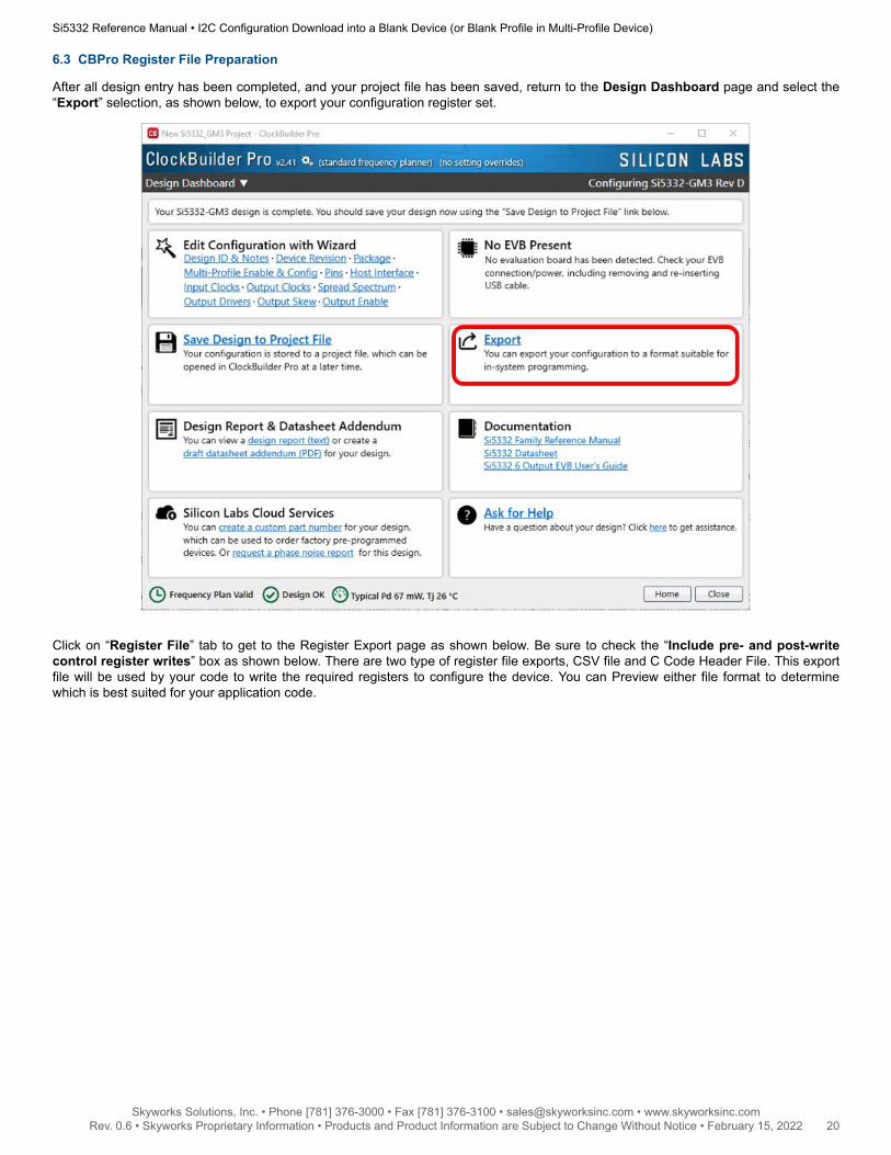
6.3 CBPro Register File Preparation
After all design entry has been completed, and your project file has been saved, return to the Design Dashboard page and select the“Export” selection, as shown below, to export your configuration register set.
Click on “Register File” tab to get to the Register Export page as shown below. Be sure to check the “Include pre- and post-writecontrol register writes” box as shown below. There are two type of register file exports, CSV file and C Code Header File. This exportfile will be used by your code to write the required registers to configure the device. You can Preview either file format to determinewhich is best suited for your application code.
Si5332 Reference Manual • I2C Configuration Download into a Blank Device (or Blank Profile in Multi-Profile Device)
Skyworks Solutions, Inc. • Phone [781] 376-3000 • Fax [781] 376-3100 • [email protected] • www.skyworksinc.com20 Rev. 0.6 • Skyworks Proprietary Information • Products and Product Information are Subject to Change Without Notice • February 15, 2022 20

6.4 I2C Download Process
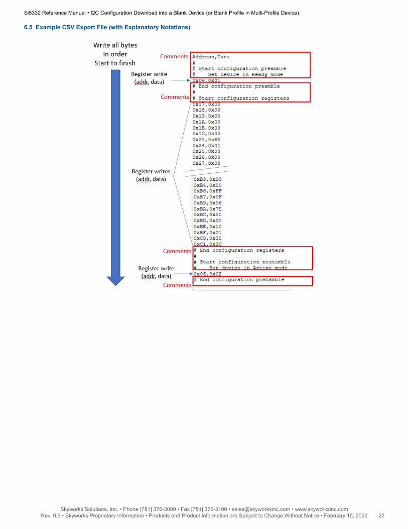
The register export files contain (address, data) pairs, either as separate lines in the CSV file, or as a C structure pairs addr, data.
Your application code should write the data byte to the addr in each (addr, data) pair in sequence, from top to bottom of file,writing ALL bytes in the file to the device being configured.
Once all writes are completed the device should start outputting active clocks according to your CBPro specified profile.
See the next page for examples of both file formats.
Si5332 Reference Manual • I2C Configuration Download into a Blank Device (or Blank Profile in Multi-Profile Device)
Skyworks Solutions, Inc. • Phone [781] 376-3000 • Fax [781] 376-3100 • [email protected] • www.skyworksinc.com21 Rev. 0.6 • Skyworks Proprietary Information • Products and Product Information are Subject to Change Without Notice • February 15, 2022 21
6.5 Example CSV Export File (with Explanatory Notations)
Si5332 Reference Manual • I2C Configuration Download into a Blank Device (or Blank Profile in Multi-Profile Device)
Skyworks Solutions, Inc. • Phone [781] 376-3000 • Fax [781] 376-3100 • [email protected] • www.skyworksinc.com22 Rev. 0.6 • Skyworks Proprietary Information • Products and Product Information are Subject to Change Without Notice • February 15, 2022 22

6.6 Example C Code Header File
/* * Si5332-GM3 Rev D Configuration Register Export Header File * * This file represents a series of Skyworks Si5332-GM3 Rev D * register writes that can be performed to load a single configuration * on a device. It was created by a Skyworks ClockBuilder Pro * export tool. * * Part: Si5332-GM3 Rev D * Design ID: * Includes Pre/Post Download Control Register Writes: Yes * Created By: ClockBuilder Pro v2.31 [2019-03-25] * Timestamp: 2019-04-01 15:38:27 GMT-05:00 * * */#ifndef SI5332-GM3_REVD_REG_CONFIG_HEADER#define SI5332-GM3_REVD_REG_CONFIG_HEADER#define SI5332-GM3_REVD_REG_CONFIG_NUM_REGS 88
typedef struct unsigned int address; /* 8-bit register address */ unsigned char value; /* 8-bit register data */ si5332-gm3_revd_register_t;
si5332-gm3_revd_register_t const si5332-gm3_revd_registers[SI5332-GM3_REVD_REG_CONFIG_NUM_REGS] = /* Start configuration preamble */ /* Set device in Ready mode */ 0x06, 0x01 , /* End configuration preamble */
/* Start configuration registers */ 0x17, 0x00 , 0x18, 0x00 , 0x19, 0x00 , 0x1A, 0x00 , 0x1B, 0x00 , 0x1C, 0x00 , . . . 0xBD, 0x00 , 0xBE, 0x10 , 0xBF, 0x01 , 0xC0, 0x30 , 0xC1, 0x30 , /* End configuration registers */
/* Start configuration postamble */ /* Set device in Active mode */ 0x06, 0x02 , /* End configuration postamble */
Si5332 Reference Manual • I2C Configuration Download into a Blank Device (or Blank Profile in Multi-Profile Device)
Skyworks Solutions, Inc. • Phone [781] 376-3000 • Fax [781] 376-3100 • [email protected] • www.skyworksinc.com23 Rev. 0.6 • Skyworks Proprietary Information • Products and Product Information are Subject to Change Without Notice • February 15, 2022 23
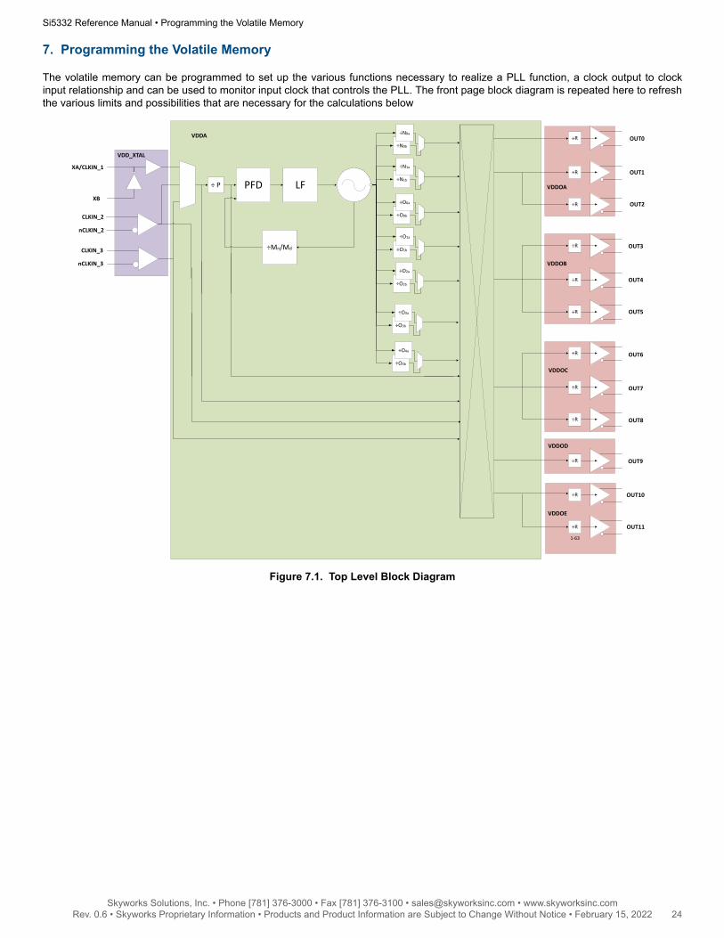
7. Programming the Volatile Memory
The volatile memory can be programmed to set up the various functions necessary to realize a PLL function, a clock output to clockinput relationship and can be used to monitor input clock that controls the PLL. The front page block diagram is repeated here to refreshthe various limits and possibilities that are necessary for the calculations below
÷ P PFD LF
÷Mn/Md
÷R
÷R
÷R
÷R
÷R
÷R
÷R
÷R
÷R
÷R
÷R
÷R
1-63
VDD_XTAL
VDDA
VDDOA
VDDOB
VDDOC
VDDOD
VDDOE
XA/CLKIN_1
XB
CLKIN_2
nCLKIN_2
CLKIN_3
nCLKIN_3
OUT0
OUT1
OUT2
OUT3
OUT4
OUT5
OUT6
OUT7
OUT8
OUT9
OUT10
OUT11
÷N0b
÷N0a
÷N1b
÷N1a
÷O0b
÷O0a
÷O1b
÷O1a
÷O2b
÷O2a
÷O3b
÷O3a
÷O4b
÷O4a
Figure 7.1. Top Level Block Diagram
Si5332 Reference Manual • Programming the Volatile Memory
Skyworks Solutions, Inc. • Phone [781] 376-3000 • Fax [781] 376-3100 • [email protected] • www.skyworksinc.com24 Rev. 0.6 • Skyworks Proprietary Information • Products and Product Information are Subject to Change Without Notice • February 15, 2022 24
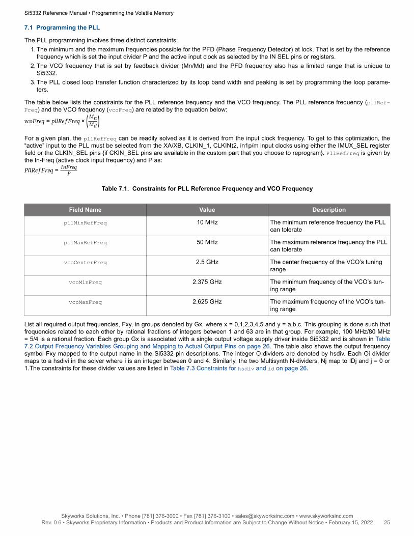
7.1 Programming the PLL
The PLL programming involves three distinct constraints:1. The minimum and the maximum frequencies possible for the PFD (Phase Frequency Detector) at lock. That is set by the reference
frequency which is set the input divider P and the active input clock as selected by the IN SEL pins or registers.2. The VCO frequency that is set by feedback divider (Mn/Md) and the PFD frequency also has a limited range that is unique to
Si5332.3. The PLL closed loop transfer function characterized by its loop band width and peaking is set by programming the loop parame-
ters.
The table below lists the constraints for the PLL reference frequency and the VCO frequency. The PLL reference frequency (pllRef-Freq) and the VCO frequency (vcoFreq) are related by the equation below:
vcoFreq = pllRe f Freq ×MnMd
For a given plan, the pllRefFreq can be readily solved as it is derived from the input clock frequency. To get to this optimization, the“active” input to the PLL must be selected from the XA/XB, CLKIN_1, CLKIN)2, in1p/m input clocks using either the IMUX_SEL registerfield or the CLKIN_SEL pins if CKIN_SEL pins are available in the custom part that you choose to reprogram. PllRefFreq is given bythe In-Freq (active clock input frequency) and P as:PllRe f Freq = InFreq
P
Table 7.1. Constraints for PLL Reference Frequency and VCO Frequency
Field Name Value Description
pllMinRefFreq 10 MHz The minimum reference frequency the PLLcan tolerate
pllMaxRefFreq 50 MHz The maximum reference frequency the PLLcan tolerate
vcoCenterFreq 2.5 GHz The center frequency of the VCO’s tuningrange
vcoMinFreq 2.375 GHz The minimum frequency of the VCO’s tun-ing range
vcoMaxFreq 2.625 GHz The maximum frequency of the VCO’s tun-ing range
List all required output frequencies, Fxy, in groups denoted by Gx, where x = 0,1,2,3,4,5 and y = a,b,c. This grouping is done such thatfrequencies related to each other by rational fractions of integers between 1 and 63 are in that group. For example, 100 MHz/80 MHz= 5/4 is a rational fraction. Each group Gx is associated with a single output voltage supply driver inside Si5332 and is shown in Table7.2 Output Frequency Variables Grouping and Mapping to Actual Output Pins on page 26. The table also shows the output frequencysymbol Fxy mapped to the output name in the Si5332 pin descriptions. The integer O-dividers are denoted by hsdiv. Each Oi dividermaps to a hsdivi in the solver where i is an integer between 0 and 4. Similarly, the two Multisynth N-dividers, Nj map to IDj and j = 0 or1.The constraints for these divider values are listed in Table 7.3 Constraints for hsdiv and id on page 26.
Si5332 Reference Manual • Programming the Volatile Memory
Skyworks Solutions, Inc. • Phone [781] 376-3000 • Fax [781] 376-3100 • [email protected] • www.skyworksinc.com25 Rev. 0.6 • Skyworks Proprietary Information • Products and Product Information are Subject to Change Without Notice • February 15, 2022 25
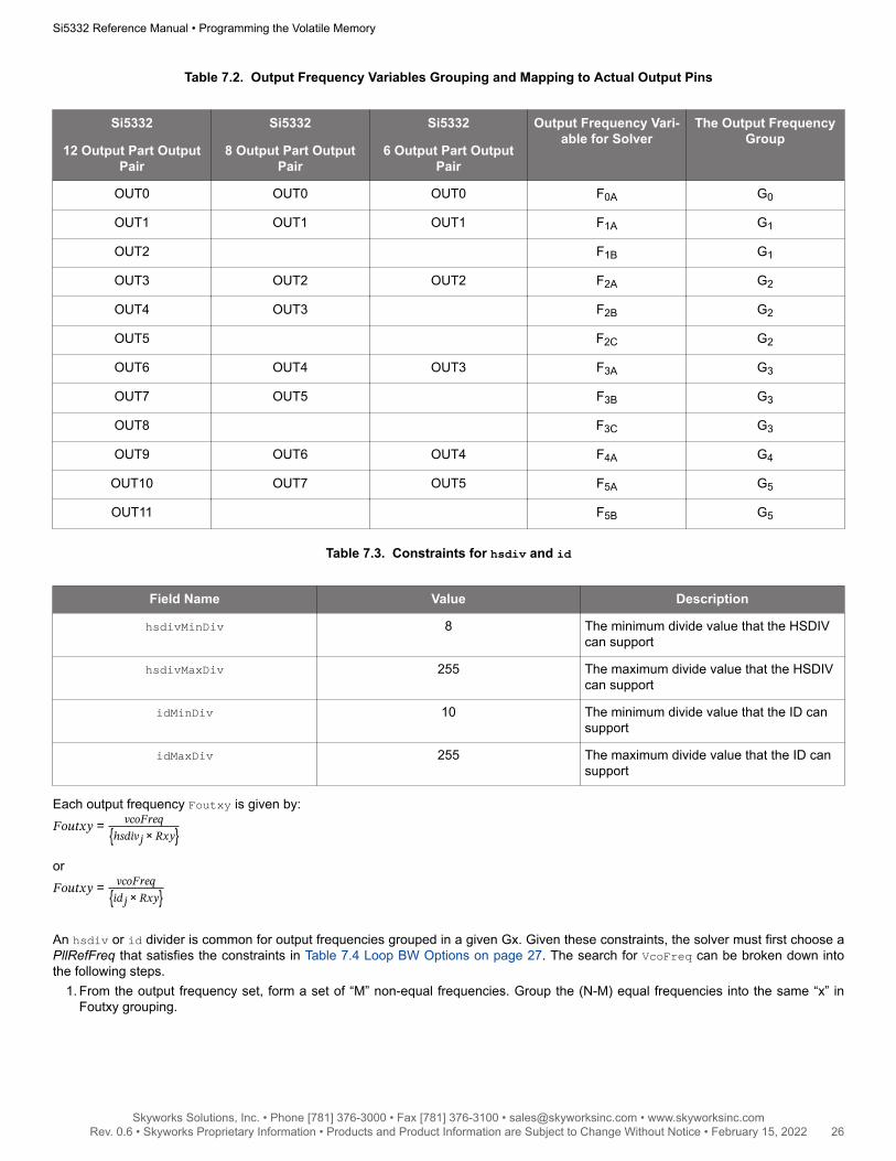
Table 7.2. Output Frequency Variables Grouping and Mapping to Actual Output Pins
Si5332
12 Output Part OutputPair
Si5332
8 Output Part OutputPair
Si5332
6 Output Part OutputPair
Output Frequency Vari-able for Solver
The Output FrequencyGroup
OUT0 OUT0 OUT0 F0A G0
OUT1 OUT1 OUT1 F1A G1
OUT2 F1B G1
OUT3 OUT2 OUT2 F2A G2
OUT4 OUT3 F2B G2
OUT5 F2C G2
OUT6 OUT4 OUT3 F3A G3
OUT7 OUT5 F3B G3
OUT8 F3C G3
OUT9 OUT6 OUT4 F4A G4
OUT10 OUT7 OUT5 F5A G5
OUT11 F5B G5
Table 7.3. Constraints for hsdiv and id
Field Name Value Description
hsdivMinDiv 8 The minimum divide value that the HSDIVcan support
hsdivMaxDiv 255 The maximum divide value that the HSDIVcan support
idMinDiv 10 The minimum divide value that the ID cansupport
idMaxDiv 255 The maximum divide value that the ID cansupport
Each output frequency Foutxy is given by:Foutxy = vcoFreq
ℎsdivj × Rxy
orFoutxy = vcoFreq
idj × Rxy
An hsdiv or id divider is common for output frequencies grouped in a given Gx. Given these constraints, the solver must first choose aPllRefFreq that satisfies the constraints in Table 7.4 Loop BW Options on page 27. The search for VcoFreq can be broken down intothe following steps.
1. From the output frequency set, form a set of “M” non-equal frequencies. Group the (N-M) equal frequencies into the same “x” inFoutxy grouping.
Si5332 Reference Manual • Programming the Volatile Memory
Skyworks Solutions, Inc. • Phone [781] 376-3000 • Fax [781] 376-3100 • [email protected] • www.skyworksinc.com26 Rev. 0.6 • Skyworks Proprietary Information • Products and Product Information are Subject to Change Without Notice • February 15, 2022 26

2. Now form MC2 groups of M-2 output frequencies. Find the LCM of each group and find an integer “I” that can such that:a.vcoFreq = I*LCM can meet the constraint for vcoFreq in Table 7.1 Constraints for PLL Reference Frequency and VCO
Frequency on page 25.b. List the “L” groups that provide a legal vcoFreq, i.e. a vcoFreq that satisfies the condition in step a.c. Choose the vcoFreq that has most number of performance critical clocks that do not need “spread spectrum” clock-ing as part
of the “M-2” output clocks
Given that vcoFreq, calculate the feedback divider as:MnMd
= vcoFreqpllRe f Freq
The Mn/Md fraction is represented in register fields IDPA_INTG, IDPA_RES and IDPA_DENIDPA_INTG = f loor 128 × vcoFreq
pllRe f Freq
IDPA_RESIDPA_DEN = 128 × vcoFreq
pllRe f Freq − IDPA_INTG
As can be seen from the above equations, the ratio IDPA_RES/ IDPA_DEN will always be less than 1.
Note: All these register fields are 15 bits wide. Therefore, the fraction will need to truncate to up to this precision. This section fullydetermines the VCO frequency, the P-divider and the feedback divider for this plan given the choice of using O-dividers HSDIV forM-2 output clocks and N-dividers ID for two output clocks.
The next step will be to determine the closed loop response that is required from the PLL. The table below lists the different loop BWsettings possible and the register field value that will enable that loop BW setting:
Table 7.4. Loop BW Options
PLL_MODE Loop Bandwidth (kHz) PLL. Ref. Freq. Min (MHz) PLL. Ref. Freq. Max. (MHz)
0 ILLEGAL IF PLL MODE IS ENABLED
1 350 10 15
2 250 10 15
3 175 10 15
4 500 15 30
5 350 15 30
6 250 15 30
7 175 15 30
8 500 30 50
9 350 30 50
10 250 30 50
11 175 30 50
This algorithm will result in a final solution for a VCO frequency, vcoFreq, that can then be used to calculate the O-divider , N-divider,and R-divider values needed to derive each output frequency, Foutxy.
Si5332 Reference Manual • Programming the Volatile Memory
Skyworks Solutions, Inc. • Phone [781] 376-3000 • Fax [781] 376-3100 • [email protected] • www.skyworksinc.com27 Rev. 0.6 • Skyworks Proprietary Information • Products and Product Information are Subject to Change Without Notice • February 15, 2022 27

7.2 Programming the Clock Path
Given a valid VCO frequency for the M unique frequencies, segregate the N-M equal frequencies into outputs from each group Gx inTable 7.2 Output Frequency Variables Grouping and Mapping to Actual Output Pins on page 26. When arranging outputs, care must betaken to minimize crosstalk (without violating the contraints imposed from the grouping of output frequencies into the VDDO “banks”).Whenever several high frequencies, fast rise time, large amplitude signals are all close to one another, the laws of physics dictate thatthere will be some amount of crosstalk. The jitter of the Si5332 is low, and, therefore, crosstalk can become a significant portion ofthe final measured output jitter. Some of the source of the crosstalk will be the Si5332 and some will be introduced by the PCB. Forextra fine tuning and optimization in addition to following the usual PCB layout guidelines, crosstalk can be minimized by modifying thearrangements of different output clocks:
1. Avoid adjacent frequency values that are close. A 155.52 MHz clock should not be next to a 156.25 MHz clock. If the jitterintegration bandwidth goes up to 20 MHz, then keep adjacent frequencies at least 20 MHz apart.
2. Adjacent frequency values that are integer multiples of one another are okay and these outputs should be grouped accordingly.3. Unused outputs can be used to separate clock outputs that might otherwise interfere with one another. If some outputs have tight
jitter requirements while others are relatively loose, rearrange the clock outputs so that the critical outputs are the least susceptibleto crosstalk. These guidelines typically only need to be followed by those applications that wish to achieve the highest possiblelevels of jitter performance. Because CMOS outputs have large pk-pk swings and do not present a balanced load to the VDDOsupplies, CMOS outputs generate much more crosstalk than differential outputs. For this reason, CMOS outputs should be avoidedwhenever possible. When CMOS is unavoidable, even greater care must be taken with respect to the above guidelines.
An output multiplexer (output mux) or crosspoint mux needs to be programmed such that each group Gx is set to the correct O-divider,N-divider, or input clock (in the case of buffering). Each output, Foutxy, has this common divider or input clock reference that needs tobe set. The multipler setting that routes the correct divider/clock source to the correct group is shown in the following table.
Table 7.5. Output Mux (Crosspoint Mux) Settings
Register field Description
omuxx_sel0 Selects output mux clock for output clocks in group Gx:
0 = PLL reference clock before pre-scaler
1 = PLL reference clock after pre-scaler
2 = Clock from input buffer 0
3 = Clock from input buffer 1
omuxx_sel1 Selects output mux clock for output clocks in group Gx:
0 = HSDIV0
1 = HSDIV1
2 = HSDIV2
3 = HSDIV3
4 = HSDIV4
5 = ID0
6 = ID1
7 = Clock from omux1_sel0
Si5332 Reference Manual • Programming the Volatile Memory
Skyworks Solutions, Inc. • Phone [781] 376-3000 • Fax [781] 376-3100 • [email protected] • www.skyworksinc.com28 Rev. 0.6 • Skyworks Proprietary Information • Products and Product Information are Subject to Change Without Notice • February 15, 2022 28

The final steps will be to program the hsdiv and id dividers. The equations below show the relationship between hsdiv, id dividervalues with their associated output frequency. They also show the register fields that need to be programmed to set up the dividervalues correctly. The register field and the divider value are both denoted by:ℎsdivxa_div = vcoFrq
Foutxa × Rxa
The id dividers are calculated as below:idxa = vcoFrq
Foutxa × Rxa
The ida fraction is represented in register fields IDPA_INTG, IDPA_RES and IDPA_DENIDxA_INTG = f loor 128 × vcoFreq
Foutxa × Rxa
IDxA_RESIDxA_DEN = 128 × vcoFreq
Foutxa × Rxa − IDxA_INTG
Si5332 Reference Manual • Programming the Volatile Memory
Skyworks Solutions, Inc. • Phone [781] 376-3000 • Fax [781] 376-3100 • [email protected] • www.skyworksinc.com29 Rev. 0.6 • Skyworks Proprietary Information • Products and Product Information are Subject to Change Without Notice • February 15, 2022 29

7.3 Programming the Output Clock Frequency
The Rxy register fields are programmed as shown in the table below. This last step completes the settings of all dividers that will resultin the frequency plan. When a valid divider solution space cannot be determined, that frequency plan is not realizable in the Si5332.
Table 7.6. Rxy to Register Field Mapping for 12-output Si5332
Divider Value Register Field Description
R0A OUT0_DIV Driver divider ratio.
0 = disabled
1–63 = divide value
R1A OUT1_DIV Driver divider ratio.
0 = disabled
1–63 = divide value
R1B OUT2_DIV Driver divider ratio.
0 = disabled
1–63 = divide value
R2A OUT3_DIV Driver divider ratio.
0 = disabled
1–63 = divide value
R2B OUT4_DIV Driver divider ratio.
0 = disabled
1–63 = divide value
R2C OUT5_DIV Driver divider ratio.
0 = disabled
1–63 = divide value
R3A OUT6_DIV Driver divider ratio.
0 = disabled
1–63 = divide value
R3B OUT7_DIV Driver divider ratio.
0 = disabled
1–63 = divide value
R3C OUT8_DIV Driver divider ratio.
0 = disabled
1–63 = divide value
R4A OUT9_DIV Driver divider ratio.
0 = disabled
1–63 = divide value
Si5332 Reference Manual • Programming the Volatile Memory
Skyworks Solutions, Inc. • Phone [781] 376-3000 • Fax [781] 376-3100 • [email protected] • www.skyworksinc.com30 Rev. 0.6 • Skyworks Proprietary Information • Products and Product Information are Subject to Change Without Notice • February 15, 2022 30

Divider Value Register Field Description
R5A OUT10_DIV Driver divider ratio.
0 = disabled
1–63 = divide value
R5B OUT11_DIV Driver divider ratio.
0 = disabled
1–63 = divide value
7.4 Programming the Output Clock Format
The following tables provide the method to fully define every driver.
Table 7.7. Driver Set Up Options
Driver Register Field Description
Driver for output OUTx OUTx_mode Software interpreted driver configuration.See Table 7.8 Driver Mode Options onpage 32.
OUTx _skew Skew control. Programmed as an unsignedinteger. Can add delay of 35 ps/step up to280 ps.
OUTx _stop_highz Driver output state when stopped.
0 = low-z
1 = high-z
OUTx _cmos_inv Sets the polarity of the two outputs in dualCMOS mode.
0 = no inversion
1 = OUTx~ inverted
OUTx _cmos_slew Controls CMOS slew rate from fast to slow.
00 = fastest
01 = slow
10 = slower
11 = Slowest
OUTx _cmos_str CMOS output impedance control.
0 = 50 Ω
1 = 25 Ω
Si5332 Reference Manual • Programming the Volatile Memory
Skyworks Solutions, Inc. • Phone [781] 376-3000 • Fax [781] 376-3100 • [email protected] • www.skyworksinc.com31 Rev. 0.6 • Skyworks Proprietary Information • Products and Product Information are Subject to Change Without Notice • February 15, 2022 31

Table 7.8. Driver Mode Options
drvxy_MODE Driver Mode
0 off
1 CMOS on positive output only
2 CMOS on negative output only
3 dual CMOS outputs
4 2.5 V/3.3 V LVDS
5 1.8 V LVDS
6 2.5 V/3.3 V LVDS fast
7 1.8 V LVDS fast
8 HCSL 50 Ω (external termination)
9 HCSL 50 Ω (internal termination)
10 HCSL 42.5 Ω (external termination)
11 HCSL 42.5 Ω (internal termination)
12 LVPECL
13 Reserved
14 Reserved
15 Reserved
Si5332 Reference Manual • Programming the Volatile Memory
Skyworks Solutions, Inc. • Phone [781] 376-3000 • Fax [781] 376-3100 • [email protected] • www.skyworksinc.com32 Rev. 0.6 • Skyworks Proprietary Information • Products and Product Information are Subject to Change Without Notice • February 15, 2022 32

7.5 Programming for Frequency Select Operations
Every hsdiv and id has a Bank A and a Bank B divider. The register field names that begin with hsdivxb or idxb denote Bank Bdividers. Any FS frequency will be:FoutxyFS = vcoFreq
idxb
Or
FoutxyFS = vcoFreqℎsdivb
Any output associated with either idxa or hsdivxa can be switched into the above FS frequency. The control that selects the Bank Bdivider is as shown in table below.
Table 7.9. The Control Register Bit to Switch Frequencies
Register Field Description
hsdivx_div_sel Selects bank A or bank B divider HSDIV0 settings. The HSDIV0supports dynamic integer divider changes through this divider se-lect control bit.
0 = bank A divider
1 = bank B divider
idx_cfg_sel Output interpolative divider 0 configuration bank select. The inter-polative divider supports dynamically switching between two com-plete configurations controlled by this bit. Reconfiguration shouldbe done on the unselected bank. If ID0_CFG=0, running basedoff bank A, then bank B may be freely reconfigured and onceready all changes will be applied to the ID once ID0_CFG=1 thuschanging the ID from bank A to bank B. Spread spectrum enablefields ID0A_SS_ENA and ID0B_SS_ENA are the only exceptionand may be enabled/disabled while bank is selected.
0 = bank A
1 = bank B
In a factory-programmed part, a pin (the FS pin) can be used for the same purpose as the control registers. Once, a control bit is set,the backup divider values control the output frequency and that is described the equations below:
O-Dividerℎsdivxb_div = vcoFreq
Foutxb × Rxa
N-Divideridxb = vcoFreq
Foutxb × Rxa
The ida fraction is represented in register fields IDPB_INTG, IDPB_RES and IDPB_DENIDxB_INTG = f loor 128 × vcoFreq
Foutxb × Rxa
IDxB_RESIDxB_DEN = 128 × vcoFreq
Foutxb × Rxa − IDxB_INTG
As can be seen, the backup divider values limit the possible values for the output frequency in this backup mode. Another key featureis that the switch to a FS frequency is “glitchless”. Therefore, the recommended method for glitchless frequency updates is to programeither divider a or b (when divider b or a is currently driving the output frequency), and then switch this divider.
Si5332 Reference Manual • Programming the Volatile Memory
Skyworks Solutions, Inc. • Phone [781] 376-3000 • Fax [781] 376-3100 • [email protected] • www.skyworksinc.com33 Rev. 0.6 • Skyworks Proprietary Information • Products and Product Information are Subject to Change Without Notice • February 15, 2022 33

7.6 Programming for Spread Spectrum
Spread spectrum clocking (SSC) is available only on the multisynth outputs. Each multisynth can implement spread spectrum in eitherthe main divider or the backup divider (the FS option). Therefore, the user can program a maximum of four different spread spectrum“profiles” from the same part, although only two profile are available on outputs at any given time. The amplitude of the SSC clockfrequency (as illustrated in Figure 7.2 Illustration: Center and Down Spread SSC Clocks as Frequency vs Time Plots on page 34) isdenoted by ssc%. For example, for down spread of -0.5%, then ssc% = 0.5. For center spread of +/- 0.25%, then ssc% = 0.25. Thevariable, Amod, in the equation below is a real number representation of the ssc%, which is a percentage value. The modulation rate(also illustrated in Figure 7.2 Illustration: Center and Down Spread SSC Clocks as Frequency vs Time Plots on page 34) is denoted byFmod in the equations below.
Amod =ssc% × 2
100 for center spreadssc%
100 for down spread
idxy_ss_step_num =vcoFreqidxy
Fmod × 4
idxy_ss_step_res = Amod × idxy_den × idxy × 1282 × idxy_ss_step_num
time
frequency
F0
Fmax = F0 (1 + ssc%/100)
Fmin = F0 (1 - ssc%/100)
Fmod = one modulation cycle
Fmod = one modulation cycle
F0
frequency
time
Fmin = F0 (1 - ssc%/100)
Figure 7.2. Illustration: Center and Down Spread SSC Clocks as Frequency vs Time Plots
The table below shows the register fields (and terms) idxy_ss_step_num and idxy_ss_step_res. idxy_ss_step_num is the number offrequency steps between the mean and the maximum/minimum frequencies in SSC clocking and idxy_ss_step_res is the frequencyresolution that is required in each step. The goal is to maximize the number of steps and minimize the resolution. However, the number
Si5332 Reference Manual • Programming the Volatile Memory
Skyworks Solutions, Inc. • Phone [781] 376-3000 • Fax [781] 376-3100 • [email protected] • www.skyworksinc.com34 Rev. 0.6 • Skyworks Proprietary Information • Products and Product Information are Subject to Change Without Notice • February 15, 2022 34

of steps is set by the modulation rate (typically 30–33 kHz). The step resolution can be minimized by setting the largest value possiblefor idxy_den. Idxy_den is the denominator of the id divider and setting it as close as possible to 215 – 1 is desired.
Table 7.10. SCC Register Fields
idxy_ss_ena Spread spectrum enable. This is the only bank configuration field which may be changed dynamically whilethe bank is selected as the active bank. Users may freely enable/disable spread spectrum.
0 = spread spectrum disabled
1 = spread spectrum enabled
idxy_ss_mode Spread spectrum mode.
0 = disabled
1 = center
2 = invalid
3 = Down
idxy_ss_clk_num Number of output clocks for each frequency step.
idxy_ss_step_num Number of frequency steps in one quarter SSC modulation period, allows for frequency step every outputclock.
idxy_ss_step_intg Divide ratio spread step size.
idxy_ss_step_res Numerator of spread step size error term.
idxy_ss_step_den Denominator of spread step size error term.
To enable SSC, idxy_ss_ena needs to be set and the right mode selected in idxy_ss_mode. The number of output clocks in eachfrequency step, idxy_ss_clk_num, needs to be set to 1 and idxy_ss_step_den is the same as idxy_den and idxy_ss_step_intg isalways zero.
The following flow needs to be followed to program the registers into Si5332:1. Write 0x01h to register 0x06h and put the Si5332 into the READY state.2. Write all the relevant registers as calculated from the steps above.3. Ensure that the valid input clocks are available for the Si5332 to attempt a PLL lock.4. Write 0x02h to register 0x06h and put the Si5332 into the ACTIVE state.
Register names are shown above in generic format such as "idxy_..." where the "xy" is a wildcard substitution where "x"refers to the Ndivider number (either 0 or 1) and "y" refers to the N divider register set (either A or B). For example, the register name for N0 dividerset A registers would start with id0a_.... and registers for N1 divider set B would start with id1b_.
Si5332 Reference Manual • Programming the Volatile Memory
Skyworks Solutions, Inc. • Phone [781] 376-3000 • Fax [781] 376-3100 • [email protected] • www.skyworksinc.com35 Rev. 0.6 • Skyworks Proprietary Information • Products and Product Information are Subject to Change Without Notice • February 15, 2022 35
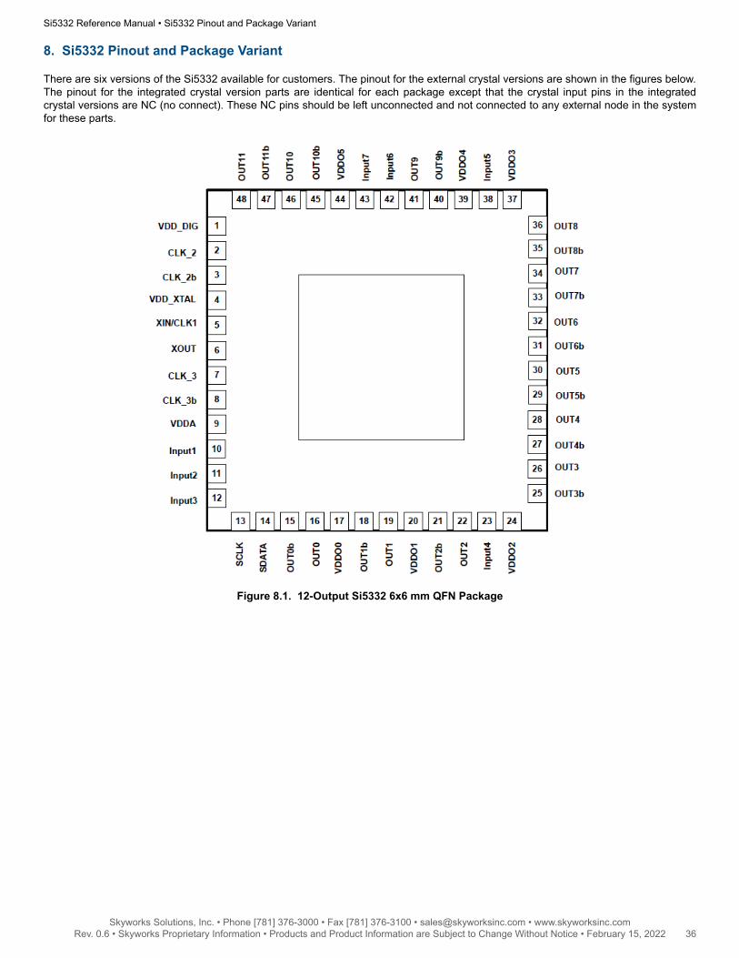
8. Si5332 Pinout and Package Variant
There are six versions of the Si5332 available for customers. The pinout for the external crystal versions are shown in the figures below.The pinout for the integrated crystal version parts are identical for each package except that the crystal input pins in the integratedcrystal versions are NC (no connect). These NC pins should be left unconnected and not connected to any external node in the systemfor these parts.
Figure 8.1. 12-Output Si5332 6x6 mm QFN Package
Si5332 Reference Manual • Si5332 Pinout and Package Variant
Skyworks Solutions, Inc. • Phone [781] 376-3000 • Fax [781] 376-3100 • [email protected] • www.skyworksinc.com36 Rev. 0.6 • Skyworks Proprietary Information • Products and Product Information are Subject to Change Without Notice • February 15, 2022 36

Figure 8.2. 8-Output Si5332 6x6 mm QFN Package
Figure 8.3. 6-Output Si5332 5x5 mm QFN Package
Si5332 Reference Manual • Si5332 Pinout and Package Variant
Skyworks Solutions, Inc. • Phone [781] 376-3000 • Fax [781] 376-3100 • [email protected] • www.skyworksinc.com37 Rev. 0.6 • Skyworks Proprietary Information • Products and Product Information are Subject to Change Without Notice • February 15, 2022 37

9. Recommended Schematic and Layout Practices
The Si5332 schematic and layout design can be referenced from the EVB design for Si5332. For each package, the user’s guide (linksbelow) outlines the EVB design and provides links to schematic and layout references for each package type.• UG301: Si5332-12EX-EVB User's Guide• UG300: Si5332-8EX-EVB User's Guide• UG299: Si5332-6EX-EVB User's Guide• UG328: Si5332-6IX-EVB User's Guide• UG329: Si5332-8IX-EVB User's Guide• UG330: Si5332-12IX-EVB User's Guide
At the schematic/placement/layout design time, these are the following guidelines:1. Power supply filtering:
a. The Si5332 can tolerate up to 100 mV (+/-50 mV) of noise for each supply node. The application note, AN1107: Si5332 PowerSupply Noise Rejection, provides the performance to be expected with such a noise.
i. As can be seen, this noise can be from a switched mode power supply (which causes noise over a wide band offrequencies) or can be noise due to some oscillatory behavior from a LDO regulator.
ii. The only filtering needed on each supply node is a 1 μF and a 0.1 μF placed as close as possible to that node.iii. The Si5332 EVBs have a much larger capacitance on the regulator end, mainly to compensate for the regulator loop so
that there is no oscillatory behavior from the regulators regardless of the voltage supply value set for that regulator. Theregulator supply design on the EVB is not required for Si5332 in system designs.
2. Crystal placement:a. The crystals should be placed as close as possible to the XA/XB pins. This placement ensures that the crystal oscillator traces
do not cause undue delays and hence, cause either an unusually long crystal start up time or get susceptible to crosstalk andthereby increase jitter on the output clocks.
Si5332 Reference Manual • Recommended Schematic and Layout Practices
Skyworks Solutions, Inc. • Phone [781] 376-3000 • Fax [781] 376-3100 • [email protected] • www.skyworksinc.com38 Rev. 0.6 • Skyworks Proprietary Information • Products and Product Information are Subject to Change Without Notice • February 15, 2022 38

10. Register Map
All common registers are listed in the table below. The registers that are specific to the 32-QFN part are listed in Table 12.1 Si5332 32QFN Registers on page 49. The registers that are specific to the 40-QFN part are listed in Table 13.1 Si5332 40 QFN Registers onpage 54. The registers that are specific to the 48-QFN part are listed in Table 14.1 Si5332 48 QFN Registers on page 60. The fieldsin these tables are the register field name, address, base, bit length, “R/W/RW”, description, and device mode. Note that all registershold values that are "big-endian", i.e., bit 7 is the MSB in an eight-bit field.
The definitions for these fields are:1. Register Field Name: The name for the register field in this FRM as referenced in the tables below and in other sections in this
FRM.2. Address: The 8-bit register address to be used in the I2C transactions when the register field needs to be addressed.3. Base: Every register field address addresses an 8-bit wide location. However, the register field may not occupy that entire location.
In those cases, they may also not start at the LSB i.e. bit #0 of that location. Base provides the bit #i from which this register fieldbegins in the addressed location.
4. Bit Length: Bit length indicates the “number of bits” that the register field occupies in the addressed location5. R/W/RW: This field indicates if the register field is Read only (R), Write only (W) or Read/Write (RW).6. Description: Description is an explanation on the purpose and programmability offered by the register field.7. I: Device mode is the mode of Si5332 in which the register field can be accessed. Si5332 has two modes of function “READY”
where the Si5332 is ready for programming in which time there will no outputs from Si5332 and “ACTIVE” where the Si5332 isactively locked to an input and is providing outputs. Some register fields can be pro-gramed in either READY or ACTIVE mode(READY/ACTIVE) whereas others can only be programmed in READY mode (READY). Device mode provides input on whichmode applies to a register field a user intends to modify.
Si5332 Reference Manual • Register Map
Skyworks Solutions, Inc. • Phone [781] 376-3000 • Fax [781] 376-3100 • [email protected] • www.skyworksinc.com39 Rev. 0.6 • Skyworks Proprietary Information • Products and Product Information are Subject to Change Without Notice • February 15, 2022 39

11. Si5332 Common Registers
Table 11.1. Si5332 Register Map
Register Field Name Address Base BitLength
R/W/RW Description DeviceMode
VDD_XTAL_OK 5 7 1 R Flag that VDDI is greater than its minimum lev-el, which is about 1.5 V.
READY/ACTIVE
VDDO_OK 5 0 6 R Each bit in the VDDO_OK register field indi-cates that a specific VDDO supply is above 1.2V, with bit position corresponding to a VDDOsupply number. Bit 0 is VDDO0 status, Bit 1 isVDDO1 status, Bit 2 is VDDO2 status, and soon up to Bit 5 is VDDO5 status.
USYS_CTRL 6 0 8 RW User System Control. Use this write-only reg-ister to command the device to transition toACTIVE or READY state. (Use USYS_STAT toread present state.) Write 0x01 to commanddevice to enter READY state. Write 0x02 to en-ter ACTIVE state.
READY/ACTIVE
USYS_STAT 7 0 8 R User System Status. This read-only register in-dicates the present device operational state.Can be used with USYS_CTRL to confirm de-vice has entered the commanded state (i.e.,ACTIVE or READY). Reading 0x01 indicatesthe device is in READY state. 0x02 indicatesthe device is in ACTIVE state. If 0x89 is read,this indicates the device has not detected an in-put clock source and can't proceed to ACTIVEstate.
READY/ACTIVE
UDRV_OE_ENA 8 0 1 RW User master output enable. Resets to 1. Thisbit controls simultaneously the driver start for alldrivers.
READY/ACTIVE
USER_SCRATCH0 9 0 8 RW User scratch pad registers, freely R/W anytime. This is just run time scratch area, not ini-tialized from NVM. The reset value is 0x00 forall bytes. Can be I2C read and written any time.
READY/ACTIVE
USER_SCRATCH1 A 0 8 RW
USER_SCRATCH2 B 0 8 RW
USER_SCRATCH3 C 0 8 RW
Si5332 Reference Manual • Si5332 Common Registers
Skyworks Solutions, Inc. • Phone [781] 376-3000 • Fax [781] 376-3100 • [email protected] • www.skyworksinc.com40 Rev. 0.6 • Skyworks Proprietary Information • Products and Product Information are Subject to Change Without Notice • February 15, 2022 40

Register Field Name Address Base BitLength
R/W/RW Description DeviceMode
DEVICE_PN_BASE D 0 8 R Device PN READY/ACTIVE
DEVICE_REV E 0 8 R Device revision
DEVICE_GRADE F 0 8 R Device grade information
FACTORY_OPN_ID0 10 0 4 R The Orderable part number identification, OPNID-0.For example, in Si5332AC93541-GM3, 9 isID-0.
FACTORY_OPN_ID1 10 4 4 R The Orderable part number identification, OPNID-0.For example, in Si5332AC93541-GM3, 9 isID-0.
FACTORY_OPN_ID2 11 4 4 R The Orderable part number identification, OPNID-0.For example, in Si5332AC93541-GM3, 9 isID-0.
FACTORY_OPN_ID3 11 0 4 R The Orderable part number identification, OPNID-0.For example, in Si5332AC93541-GM3, 9 isID-0.
FACTORY_OPN_ID4 12 0 4 R The Orderable part number identification, OPNID-0.For example, in Si5332AC93541-GM3, 9 isID-0.
FACTORY_OPN_RE-VISION
12 4 4 R The Orderable part number's product revisionnumber.
DESIGN_ID0 17 0 8 R Design identification set by user in CBProproject file
DESIGN_ID1 18 0 8 R
DESIGN_ID2 19 0 8 R
I2C_ADDR 21 0 7 R I2C mode device address. Reset value is110_1010 binary.
I2C_SCL_PUP_ENA 23 0 1 RW Enable 50 kΩ pullup resistor on SCL pad. READY/ACTIVE
I2C_SDA_PUP_ENA 23 1 1 RW Enable 50 kΩ pullup resistor on SDA pad. READY/ACTIVE
OMUX0_SEL0 25 0 2 RW Selects output mux clock source for outputclocks in group G0:OUT0:
0 = PLL reference clock before P-divider
1 = PLL reference clock after P-divider
2 = Clock from input buffer CLKIN_2
3 = Clock from input buffer CLKIN_3
READY/ACTIVE
Si5332 Reference Manual • Si5332 Common Registers
Skyworks Solutions, Inc. • Phone [781] 376-3000 • Fax [781] 376-3100 • [email protected] • www.skyworksinc.com41 Rev. 0.6 • Skyworks Proprietary Information • Products and Product Information are Subject to Change Without Notice • February 15, 2022 41

Register Field Name Address Base BitLength
R/W/RW Description DeviceMode
OMUX0_SEL1 25 4 3 RW Selects output mux clock source for outputclocks in group G0:OUT0:
0 = HSDIV0
1 = HSDIV1
2 = HSDIV2
3 = HSDIV3
4 = HSDIV4
5 = ID0
6 = ID1
7 = Clock from OMUX0_SEL0
Note that the OMUX0_SEL1 value is forced to7 whenever the PLL is disabled
READY/ACTIVE
OMUX1_SEL0 26 0 2 RW Selects output mux clock source for outputclocks in group G1:OUT1 for GM1,GM2.OUT1,OUT2 for GM3:
0 = PLL reference clock before prescaler
1 = PLL reference clock after prescaler
2 = Clock from input buffer CLKIN_2
3 = Clock from input buffer CLKIN_3
READY/ACTIVE
OMUX1_SEL1 26 4 3 RW Selects output mux clock source for outputclocks in group G1:OUT1 for GM1,GM2.OUT1,OUT2 for GM3:
0 = HSDIV0
1 = HSDIV1
2 = HSDIV2
3 = HSDIV3
4 = HSDIV4
5 = ID0
6 = ID1
7 = Clock from OMUX0_SEL0
Note that the OMUX0_SEL1 value is forced to7 whenever the PLL is disabled
READY/ACTIVE
OMUX2_SEL0 27 0 2 RW Selects output mux clock source for out-put clocks in group G2:OUT2 for GM1.OUT2,OUT3 for GM2. OUT3,OUT4,OUT5 forGM3:
0 = PLL reference clock before prescaler
1 = PLL reference clock after prescaler
2 = Clock from input buffer CLKIN_2
3 = Clock from input buffer CLKIN_3
READY/ACTIVE
Si5332 Reference Manual • Si5332 Common Registers
Skyworks Solutions, Inc. • Phone [781] 376-3000 • Fax [781] 376-3100 • [email protected] • www.skyworksinc.com42 Rev. 0.6 • Skyworks Proprietary Information • Products and Product Information are Subject to Change Without Notice • February 15, 2022 42

Register Field Name Address Base BitLength
R/W/RW Description DeviceMode
OMUX2_SEL1 27 4 3 RW READY/ACTIVE
OMUX3_SEL0 28 0 2 RW Selects output mux clock source for out-put clocks in group G3:OUT3 for GM1.OUT4,OUT5 for GM2. OUT6, OUT7, OUT8 forGM3:
0 = PLL reference clock before prescaler
1 = PLL reference clock after prescaler
2 = Clock from input buffer CLKIN_2
3 = Clock from input buffer CLKIN_3
READY/ACTIVE
OMUX3_SEL1 28 4 3 RW Selects output mux clock source for out-put clocks in group G3:OUT3 for GM1.OUT4,OUT5 for GM2. OUT6,OUT7,OUT8 forGM3:
0 = HSDIV0
1 = HSDIV1
2 = HSDIV2
3 = HSDIV3
4 = HSDIV4
5 = ID0
6 = ID1
7 = Clock from OMUX0_SEL0
Note that the OMUX0_SEL1 value is forced to7 whenever the PLL is disabled
READY/ACTIVE
OMUX4_SEL0 29 0 2 RW Selects output mux clock source for outputclocks in group G4:OUT4 for GM1. OUT6 forGM2. OUT9 for GM3:
0 = PLL reference clock before prescaler
1 = PLL reference clock after prescaler
2 = Clock from input buffer CLKIN_2
3 = Clock from input buffer CLKIN_3
READY/ACTIVE
Si5332 Reference Manual • Si5332 Common Registers
Skyworks Solutions, Inc. • Phone [781] 376-3000 • Fax [781] 376-3100 • [email protected] • www.skyworksinc.com43 Rev. 0.6 • Skyworks Proprietary Information • Products and Product Information are Subject to Change Without Notice • February 15, 2022 43

Register Field Name Address Base BitLength
R/W/RW Description DeviceMode
OMUX4_SEL1 29 4 3 RW Selects output mux clock source for outputclocks in group G4:OUT4 for GM1. OUT6 forGM2. OUT9 for GM3:
0 = HSDIV0
1 = HSDIV1
2 = HSDIV2
3 = HSDIV3
4 = HSDIV4
5 = ID0
6 = ID1
7 = Clock from OMUX0_SEL0
Note that the OMUX0_SEL1 value is forced to7 whenever the PLL is disabled
READY/ACTIVE
OMUX5_SEL0 2A 0 2 RW Selects output mux clock source for outputclocks in group G5:OUT5 for GM1. OUT7 forGM2. OUT10,OUT11 for GM3:
0 = PLL reference clock before prescaler
1 = PLL reference clock after prescaler
2 = Clock from input buffer CLKIN_2
3 = Clock from input buffer CLKIN_3
READY/ACTIVE
OMUX5_SEL1 2A 4 3 RW Selects output mux clock source for outputclocks in group G5:OUT5 for GM1. OUT7 forGM2. OUT10,OUT11 for GM3:
0 = HSDIV0
1 = HSDIV1
2 = HSDIV2
3 = HSDIV3
4 = HSDIV4
5 = ID0
6 = ID1
7 = Clock from OMUX0_SEL0
Note that the OMUX0_SEL1 value is forced to7 whenever the PLL is disabled
READY/ACTIVE
HSDIV0A_DIV 2B 0 8 RW O0 divider value READY ifdivider iscurrently
driving theoutputelse
READY/ACTIVE
HSDIV0B_DIV 2C 0 8 RW O0 divider value for bank A
Si5332 Reference Manual • Si5332 Common Registers
Skyworks Solutions, Inc. • Phone [781] 376-3000 • Fax [781] 376-3100 • [email protected] • www.skyworksinc.com44 Rev. 0.6 • Skyworks Proprietary Information • Products and Product Information are Subject to Change Without Notice • February 15, 2022 44

Register Field Name Address Base BitLength
R/W/RW Description DeviceMode
HSDIV1A_DIV 2D 0 8 RW O1 divider value for bank A
HSDIV1B_DIV 2E 0 8 RW O1 divider value for bank B
HSDIV2A_DIV 2F 0 8 RW O2 divider value for bank A
HSDIV2B_DIV 30 0 8 RW O2 divider value for bank B
HSDIV3A_DIV 31 0 8 RW O3 divider value for bank A
HSDIV3B_DIV 32 0 8 RW O3 divider value for bank B
HSDIV4A_DIV 33 0 8 RW O4 divider value for bank A
HSDIV4B_DIV 34 0 8 RW O4 divider value for bank B
HSDIV3_DIV_SEL 35 3 1 RW Selects bank A (0) or bank B (1) O3 divid-er settings. Same description applies as forHSDIV0_DIV_SEL.
READY/ACTIVE
ID0_CFG_SEL 35 6 1 RW N0 configuration bank select. The divider sup-ports dynamically switching between two com-plete configurations controlled by this bit. Re-configuration should be done on the unselectedbank. If ID0_CFG=0, running based off bankA, then bank B may be freely reconfigured andonce ready all changes will be applied to theID once ID0_CFG=1 thus changing the ID frombank A to bank B. Spread spectrum enablefields ID0A_SS_ENA and ID0B_SS_ENA arethe only exception and may be enabled/disa-bled while bank is selected.
0 = bank A
1 = bank B
READY/ACTIVE
HSDIV4_DIV_SEL 35 4 1 RW Selects bank A (0) or bank B (1) O4 divid-er settings. Same description applies as forHSDIV0_DIV_SEL.
READY/ACTIVE
ID1_CFG_SEL 35 7 1 RW N1 configuration bank select. Same descriptionrelated to ID1 applies as in the ID0_CFG de-scription.
0 = bank A
1 = bank B
READY/ACTIVE
HSDIV2_DIV_SEL 35 2 1 RW Selects bank A (0) or bank B (1) O2 divid-er settings. Same description applies as forHSDIV0_DIV_SEL.
READY/ACTIVE
HSDIV0_DIV_SEL 35 0 1 RW Selects bank A or bank B divider O0 settings.O0 supports dynamic integer divider changesthrough this divider select control bit.
0 = bank A divider
1 = bank B divider
READY/ACTIVE
HSDIV1_DIV_SEL 35 1 1 RW Selects bank A (0) or bank B (1) O1 divid-er settings. Same description applies as forHSDIV0_DIV_SEL.
READY/ACTIVE
Si5332 Reference Manual • Si5332 Common Registers
Skyworks Solutions, Inc. • Phone [781] 376-3000 • Fax [781] 376-3100 • [email protected] • www.skyworksinc.com45 Rev. 0.6 • Skyworks Proprietary Information • Products and Product Information are Subject to Change Without Notice • February 15, 2022 45

Register Field Name Address Base BitLength
R/W/RW Description DeviceMode
ID0A_INTG 36 0 15 RW The terms of an a + b/c desired dividersetting must be processsed into ID0A_INTG,ID0A_RES, and ID0A_DEN register terms.intg= floor(((a*c+b)*128/c) - 512).
READY ifdivider iscurrently
driving theoutputelse
READY/ACTIVE
ID0A_RES 38 0 15 RW res = mod(b*128, c)
ID0A_DEN 3A 0 15 RW den = c
ID0A_SS_ENA 3C 0 1 RW Spread spectrum enable. This is the only bankconfiguration field which may be changed dy-namically while the bank is selected as theactive bank. Users may freely enable/disablespread spectrum.
0 = spread spectrum disabled
1 = spread spectrum enabled
READY/ACTIVE
ID0A_SS_MODE 3C 1 2 RW Spread spectrum mode.
0 = disabled
1 = center
2 = invalid
3 = Down
READY ifdivider iscurrently
driving theoutputelse
READY/ACTIVE
ID0A_SS_STEP_NUM 3D 0 12 RW Number of frequency steps in one quarter SSCmodulation period, allows for frequency stepevery output clock.
ID0A_SS_STEP_INTG 3F 0 5 RW Divide ratio spread step size.
ID0A_SS_STEP_RES 40 0 15 RW Numerator of spread step size error term.
ID0B_INTG 42 0 15 RW The terms of an a + b/c desired dividersetting must be processed into ID0B_INTG,ID0B_RES, and ID0B_DEN register terms.intg= floor(((a*c+b)*128/c) - 512).
READY ifdivider iscurrently
driving theoutputelse
READY/ACTIVE
ID0B_RES 44 0 15 RW res = mod(b*128, c)
ID0B_DEN 46 0 15 RW den = c
ID0B_SS_ENA 48 0 1 RW Spread spectrum enable. This is the only bankconfiguration field which may be changed dy-namically while the bank is selected as theactive bank. Users may freely enable/disablespread spectrum.
0 = spread spectrum disabled
1 = spread spectrum enabled
READY/ACTIVE
Si5332 Reference Manual • Si5332 Common Registers
Skyworks Solutions, Inc. • Phone [781] 376-3000 • Fax [781] 376-3100 • [email protected] • www.skyworksinc.com46 Rev. 0.6 • Skyworks Proprietary Information • Products and Product Information are Subject to Change Without Notice • February 15, 2022 46

Register Field Name Address Base BitLength
R/W/RW Description DeviceMode
ID0B_SS_MODE 48 1 2 RW Spread spectrum mode.
0 = disabled
1 = center
2 = invalid
3 = Down
READY ifdivider iscurrently
driving theoutputelse
READY/ACTIVE
ID0B_SS_STEP_NUM 49 0 12 RW Number of frequency steps in one quarter SSCmodulation period, allows for frequency stepevery output clock.
ID0B_SS_STEP_INTG 4B 0 5 RW Divide ratio spread step size.
ID0B_SS_STEP_RES 4C 0 15 RW Numerator of spread step size error term.
ID1A_INTG 4E 0 15 RW The terms of an a + b/c desired interpola-tive divider setting must be processed intoID1A_INTG, ID1A_RES, and ID1A_DEN regis-ter terms.intg = floor(((a*c+b)*128/c) - 512).
READY ifdivider iscurrently
driving theoutputelse
READY/ACTIVE
ID1A_RES 50 0 15 RW res = mod(b*128, c)
ID1A_DEN 52 0 15 RW den = c
ID1A_SS_ENA 54 0 1 RW Spread spectrum enable. This is the only bankconfiguration field which may be changed dy-namically while the bank is selected as theactive bank. Users may freely enable/disablespread spectrum.
0 = spread spectrum disabled
1 = spread spectrum enabled
READY/ACTIVE
ID1A_SS_MODE 54 1 2 RW Spread spectrum mode.
0 = disabled
1 = center
2 = invalid (up)
3 = Down
READY ifdivider iscurrently
driving theoutputelse
READY/ACTIVE
ID1A_SS_STEP_NUM 55 0 12 RW Number of frequency steps in one quadrate,allows for frequency step every output clock.
ID1A_SS_STEP_INTG 57 0 5 RW Divide ratio spread step size.
ID1A_SS_STEP_RES 58 0 15 RW Numerator of spread step size error term.
ID1B_INTG 5A 0 15 RW The terms of an a + b/c desired interpola-tive divider setting must be processed intoID1A_INTG, ID1A_RES, and ID1A_DEN regis-ter terms.intg = floor(((a*c+b)*128/c) - 512).
READY ifdivider iscurrently
driving theoutputelse
READY/ACTIVE
ID1B_RES 5C 0 15 RW res = mod(b*128, c)
ID1B_DEN 5E 0 15 RW den = c
Si5332 Reference Manual • Si5332 Common Registers
Skyworks Solutions, Inc. • Phone [781] 376-3000 • Fax [781] 376-3100 • [email protected] • www.skyworksinc.com47 Rev. 0.6 • Skyworks Proprietary Information • Products and Product Information are Subject to Change Without Notice • February 15, 2022 47

Register Field Name Address Base BitLength
R/W/RW Description DeviceMode
ID1B_SS_ENA 60 0 1 RW Spread spectrum enable. This is the only bankconfiguration field which may be changed dy-namically while the bank is selected as theactive bank. Users may freely enable/disablespread spectrum.
0 = spread spectrum disabled
1 = spread spectrum enabled
READY/ACTIVE
ID1B_SS_MODE 60 1 2 RW Spread spectrum mode.
0 = disabled
1 = center
2 = invalid (up)
3 = Down
READY ifdivider iscurrently
driving theoutputelse
READY/ACTIVE
ID1B_SS_STEP_NUM 61 0 12 RW Number of frequency steps in one quadrate,allows for frequency step every output clock.
ID1B_SS_STEP_INTG 63 0 5 RW Divide ratio spread step size.
ID1B_SS_STEP_RES 64 0 15 RW Numerator of spread step size error term.
IDPA_INTG 67 0 15 RW The terms of an a + b/c desired divider set-ting must be processed into IDPA_INTG, ID-PA_RES, and IDPA_DEN register terms.intg =floor(((a*c+b)*128/c) - 512).
READY
IDPA_RES 69 0 15 RW res = mod(b*128, c) READY
IDPA_DEN 6B 0 15 RW den = c READY
PDIV_DIV 75 0 5 RW Chooses the PLL prescalar divide ratio. READY
USYS_START B8 0 8 RW User defined application startup behavior. Flagsfor SW what to do at the startup, for examplemoving to ACTIVE on its own upon startup orwaiting in READY state for a command. Usedonly upon startup, Initialized from NVM.
READY
PLL_MODE BE 2 4 RW Sets PLL BW. See Table 7.1 Constraints forPLL Reference Frequency and VCO Frequencyon page 25.
READY
XOSC_CINT_ENA(for -EX parts only)
BF 7 1 RW Enables an additional fixed 8 pf loading capaci-tance on XA and XB.
READY
XOSC_CTRIM_XA(for -EX parts only)
C0 0 6 RW Load capacitance trim on XA. READY
XOSC_CTRIM_XB(for -EX parts only)
C1 0 6 RW Load capacitance trim on XB. READY
Si5332 Reference Manual • Si5332 Common Registers
Skyworks Solutions, Inc. • Phone [781] 376-3000 • Fax [781] 376-3100 • [email protected] • www.skyworksinc.com48 Rev. 0.6 • Skyworks Proprietary Information • Products and Product Information are Subject to Change Without Notice • February 15, 2022 48

12. Si5332 32-QFN Specific Registers
Table 12.1. Si5332 32 QFN Registers
Register Field Name Address Base BitLength
R/W/RW Description DeviceMode
OUT0_MODE 7A 0 4 RW Software interpreted driver configuration. SeeTable 7.7 Driver Set Up Options on page 31.
READY
OUT0_DIV 7B 0 6 RW Driver divider ratio.
0 = disabled
1-63 = divide value
READY
OUT0_SKEW 7C 0 3 RW Skew control. Programmed as an unsigned in-teger. Can add delay of 35 ps/step up to 280ps.
READY
OUT0_STOP_HIGHZ 7D 0 1 RW Driver output state when stopped.
0 = low-Z
1 = high-Z
READY
OUT0_CMOS_INV 7D 4 2 RW Sets the polarity of the two outputs in dualCMOS mode.
0 = no inversion
1 = OUT0b inverted
READY
OUT0_CMOS_SLEW 7E 0 2 RW Controls CMOS slew rate from fast to slow.
00 = fastest
01 = slow
10 = slower
11 = slowest
READY
OUT0_CMOS_STR 7E 2 1 RW CMOS output impedance control.
0 = 50 Ω
1 = 25 Ω
READY
OUT1_MODE 7F 0 4 RW Software interpreted driver configuration. SeeTable 7.7 Driver Set Up Options on page 31.
READY
OUT1_DIV 80 0 6 RW Driver divider ratio.
0 = disabled
1–63 = divide value
READY
OUT1_SKEW 81 0 3 RW Skew control. Programmed as an unsigned in-teger. Can add delay of 35 ps/step up to 280ps.
READY
OUT1_STOP_HIGHZ 82 0 2 RW Driver output state when stopped.
0 = low-Z
1 = high-Z
READY
Si5332 Reference Manual • Si5332 32-QFN Specific Registers
Skyworks Solutions, Inc. • Phone [781] 376-3000 • Fax [781] 376-3100 • [email protected] • www.skyworksinc.com49 Rev. 0.6 • Skyworks Proprietary Information • Products and Product Information are Subject to Change Without Notice • February 15, 2022 49

Register Field Name Address Base BitLength
R/W/RW Description DeviceMode
OUT1_CMOS_INV 82 4 1 RW Sets the polarity of the two outputs in dualCMOS mode.
0 = no inversion
1 = OUT1b inverted
READY
OUT1_CMOS_SLEW 83 0 1 RW Controls CMOS slew rate from fast to slow.
00 = fastest
01 = slow
10 = slower
11 = slowest
READY
OUT1_CMOS_STR 83 2 1 RW CMOS output impedance control.
0 = 50 Ω
1 = 25 Ω
READY
OUT2_MODE 89 0 4 RW Software interpreted driver configuration. SeeTable 7.7 Driver Set Up Options on page 31.
READY
OUT2_DIV 8A 0 6 RW Driver divider ratio.
0 = disabled
1-63 = divide value
READY
OUT2_SKEW 8B 0 3 RW Skew control. Programmed as an unsigned in-teger. Can add delay of 35 ps/step up to 280ps.
READY
OUT2_STOP_HIGHZ 8C 0 2 RW Driver output state when stopped.
0 = low-Z
1 = high-Z
READY
OUT2_CMOS_INV 8C 4 1 RW Sets the polarity of the two outputs in dualCMOS mode.
0 = no inversion
1 = OUT2b inverted
READY
OUT2_CMOS_SLEW 8D 0 2 RW Controls CMOS slew rate from fast to slow.
00 = fastest
01 = slow
10 = slower
11 = slowest
READY
OUT2_CMOS_STR 8D 2 1 RW CMOS output impedance control.
0 = 50 Ω
1 = 25 Ω
READY
OUT3_MODE 98 0 4 RW Software interpreted driver configuration. SeeTable 7.7 Driver Set Up Options on page 31.
READY
Si5332 Reference Manual • Si5332 32-QFN Specific Registers
Skyworks Solutions, Inc. • Phone [781] 376-3000 • Fax [781] 376-3100 • [email protected] • www.skyworksinc.com50 Rev. 0.6 • Skyworks Proprietary Information • Products and Product Information are Subject to Change Without Notice • February 15, 2022 50

Register Field Name Address Base BitLength
R/W/RW Description DeviceMode
OUT3_DIV 99 0 6 RW Driver divider ratio.
0 = disabled
1-63 = divide value
READY
OUT3_SKEW 9A 0 3 RW Skew control. Programmed as an unsigned in-teger. Can add delay of 35 ps/step up to 280ps.
READY
OUT3_STOP_HIGHZ 9B 0 1 RW Driver output state when stopped.
0 = low-Z
1 = high-Z
READY
OUT3_CMOS_INV 9B 4 1 RW Sets the polarity of the two outputs in dualCMOS mode.
0 = no inversion
1 = OUT3b inverted
READY
OUT3_CMOS_SLEW 9C 0 1 RW Controls CMOS slew rate from fast to slow.
00 = fastest
01 = slow
10 = slower
11 = slowest
READY
OUT3_CMOS_STR 9C 2 1 RW CMOS output impedance control.
0 = 50 Ω
1 = 25 Ω
READY
OUT4_MODE A7 0 4 RW Software interpreted driver configuration. SeeTable 7.7 Driver Set Up Options on page 31.
READY
OUT4_DIV A8 0 6 RW Driver divider ratio.
0 = disabled
1-63 = divide value
READY
OUT4_SKEW A9 0 3 RW Skew control. Programmed as an unsigned in-teger. Can add delay of 35 ps/step up to 280ps.
READY
OUT4_STOP_HIGHZ AA 0 1 RW Driver output state when stopped.
0 = low-Z
1 = high-Z
READY
OUT4_CMOS_INV AA 4 1 RW Sets the polarity of the two outputs in dualCMOS mode..
0 = no inversion
1 = OUT4b inverted
READY
Si5332 Reference Manual • Si5332 32-QFN Specific Registers
Skyworks Solutions, Inc. • Phone [781] 376-3000 • Fax [781] 376-3100 • [email protected] • www.skyworksinc.com51 Rev. 0.6 • Skyworks Proprietary Information • Products and Product Information are Subject to Change Without Notice • February 15, 2022 51
Register Field Name Address Base BitLength
R/W/RW Description DeviceMode
OUT4_CMOS_SLEW AB 0 1 RW Controls CMOS slew rate from fast to slow.
00 = fastest
01 = slow
10 = slower
11 = slowest
READY
OUT4_CMOS_STR AB 2 1 RW CMOS output impedance control.
0 = 50 Ω
1 = 25 Ω
READY
OUT5_MODE AC 0 4 RW Software interpreted driver configuration. SeeTable 7.7 Driver Set Up Options on page 31.
READY
OUT5_DIV AD 0 6 RW Driver divider ratio.
0 = disabled
1–63 = divide value
READY
OUT5_SKEW AE 0 3 RW Skew control. Programmed as an unsigned in-teger. Can add delay of 35 ps/step up to 280ps.
READY
OUT5_STOP_HIGHZ AF 0 1 RW Driver output state when stopped.
0 = low-Z
1 = high-Z
READY
OUT5_CMOS_INV AF 4 1 RW Sets the polarity of the two outputs in dualCMOS mode.
0 = no inversion
1 = OUT5b inverted
READY
OUT5_CMOS_SLEW B0 0 1 RW Controls CMOS slew rate from fast to slow.
00 = fastest
01 = slow
10 = slower
11 = slowest
READY
OUT5_CMOS_STR B0 2 1 RW CMOS output impedance control.
0 = 50 Ω
1 = 25 Ω
READY
OUT2_OE B6 3 1 RW Output enable control for OUT2 READY/ACTIVE
OUT3_OE B6 6 1 RW Output enable control for OUT3 READY/ACTIVE
OUT0_OE B6 0 1 RW Output enable control for OUT0 READY/ACTIVE
OUT1_OE B6 1 1 RW Output enable control for OUT1 READY/ACTIVE
Si5332 Reference Manual • Si5332 32-QFN Specific Registers
Skyworks Solutions, Inc. • Phone [781] 376-3000 • Fax [781] 376-3100 • [email protected] • www.skyworksinc.com52 Rev. 0.6 • Skyworks Proprietary Information • Products and Product Information are Subject to Change Without Notice • February 15, 2022 52

Register Field Name Address Base BitLength
R/W/RW Description DeviceMode
OUT5_OE B7 2 1 RW Output enable control for OUT5 READY/ACTIVE
OUT4_OE B7 1 1 RW Output enable control for OUT4 READY/ACTIVE
CLKIN_2_CLK_SEL 73 0 2 RW 0 = disabled
1 = differential
2 = CMOS DC
3 = CMOS AC
READY
IMUX_SEL 24 0 2 RW Selects input mux clock source:
0 = Disabled
1= XOSC
2 = CLKIN_2
3 =Disabled
READY
Si5332 Reference Manual • Si5332 32-QFN Specific Registers
Skyworks Solutions, Inc. • Phone [781] 376-3000 • Fax [781] 376-3100 • [email protected] • www.skyworksinc.com53 Rev. 0.6 • Skyworks Proprietary Information • Products and Product Information are Subject to Change Without Notice • February 15, 2022 53

13. Si5332 40-QFN Specific Registers
Table 13.1. Si5332 40 QFN Registers
Register Field Name Address Base BitLength
R/W/RW Description DeviceMode
OUT0_MODE 7A 0 4 RW Software interpreted driver configuration. SeeTable 7.7 Driver Set Up Options on page 31.
READY
OUT0_DIV 7B 0 6 RW Driver divider ratio.
0 = disabled
1-63 = divide value
READY
OUT0_SKEW 7C 0 3 RW Skew control. Programmed as an unsigned in-teger. Can add delay of 35 ps/step up to 280ps.
READY
OUT0_STOP_HIGHZ 7D 0 1 RW Driver output state when stopped.
0 = low-Z
1 = high-Z
READY
OUT0_CMOS_INV 7D 4 2 RW Sets the polarity of the two outputs in dualCMOS mode.
0 = no inversion
1 = OUT0b inverted
READY
OUT0_CMOS_SLEW 7E 0 2 RW Controls CMOS slew rate from fast to slow.
00 = fastest
01 = slow
10 = slower
11 = slowest
READY
OUT0_CMOS_STR 7E 2 1 RW CMOS output impedance control.
0 = 50 Ω
1 = 25 Ω
READY
OUT1_MODE 7F 0 4 RW Software interpreted driver configuration. SeeTable 7.7 Driver Set Up Options on page 31.
READY
OUT1_DIV 80 0 6 RW Driver divider ratio.
0 = disabled
1-63 = divide value
READY
OUT1_SKEW 81 0 3 RW Skew control. Programmed as an unsigned in-teger. Can add delay of 35 ps/step up to 280ps.
READY
OUT1_STOP_HIGHZ 82 0 2 RW Driver output state when stopped.
0 = low-Z
1 = high-Z
READY
Si5332 Reference Manual • Si5332 40-QFN Specific Registers
Skyworks Solutions, Inc. • Phone [781] 376-3000 • Fax [781] 376-3100 • [email protected] • www.skyworksinc.com54 Rev. 0.6 • Skyworks Proprietary Information • Products and Product Information are Subject to Change Without Notice • February 15, 2022 54

Register Field Name Address Base BitLength
R/W/RW Description DeviceMode
OUT1_CMOS_INV 82 4 1 RW Sets the polarity of the two outputs in dualCMOS mode.
0 = no inversion
1 = OUT1b inverted
READY
OUT1_CMOS_SLEW 83 0 1 RW Controls CMOS slew rate from fast to slow.
00 = fastest
01 = slow
10 = Slower
11 = slowest
READY
OUT1_CMOS_STR 83 2 1 RW CMOS output impedance control.
0 = 50 Ω
1 = 25 Ω
READY
OUT2_MODE 89 0 4 RW Software interpreted driver configuration. SeeTable 7.7 Driver Set Up Options on page 31.
READY
OUT2_DIV 8A 0 6 RW Driver divider ratio.
0 = disabled
1-63 = divide value
READY
OUT2_SKEW 8B 0 3 RW Skew control. Programmed as an unsigned in-teger. Can add delay of 35 ps/step up to 280ps.
READY
OUT2_STOP_HIGHZ 8C 0 2 RW Driver output state when stopped.
0 = low-Z
1 = high-Z
READY
OUT2_CMOS_INV 8C 4 1 RW Sets the polarity of the two outputs.
0 = no inversion
1 = OUT2b inverted
READY
OUT2_CMOS_SLEW 8D 0 2 RW Controls CMOS slew rate from fast to slow.
00 = fastest
01 = slow
10 = slower
11 = slowest
READY
OUT2_CMOS_STR 8D 2 1 RW CMOS output impedance control.
0 = 50 Ω
1 = 25 Ω
READY
OUT3_MODE 8E 0 4 RW Software interpreted driver configuration. SeeTable 7.7 Driver Set Up Options on page 31.
READY
Si5332 Reference Manual • Si5332 40-QFN Specific Registers
Skyworks Solutions, Inc. • Phone [781] 376-3000 • Fax [781] 376-3100 • [email protected] • www.skyworksinc.com55 Rev. 0.6 • Skyworks Proprietary Information • Products and Product Information are Subject to Change Without Notice • February 15, 2022 55

Register Field Name Address Base BitLength
R/W/RW Description DeviceMode
OUT3_DIV 8F 0 6 RW Driver divider ratio.
0 = disabled
1-63 = divide value
READY
OUT3_SKEW 90 0 3 RW Skew control. Programmed as an unsigned in-teger. Can add delay of 35 ps/step up to 280ps.
READY
OUT3_STOP_HIGHZ 91 0 2 RW Driver output state when stopped.
0 = low-Z
1 = high-Z
READY
OUT3_CMOS_INV 91 4 1 RW Sets the polarity of the two outputs in dualCMOS mode.
0 = no inversion
1 = OUT3b inverted
READY
OUT3_CMOS_SLEW 92 0 1 RW Controls CMOS slew rate from fast to slow.
00 = fastest
01 = slow
10 = slower
11 = slowest
READY
OUT3_CMOS_STR 92 2 1 RW CMOS output impedance control.
0 = 50 Ω
1 = 25 Ω
READY
OUT4_MODE 98 0 4 RW Software interpreted driver configuration. SeeTable 7.7 Driver Set Up Options on page 31.
READY
OUT4_DIV 99 0 6 RW Driver divider ratio.
0 = disabled
1-63 = divide value
READY
OUT4_SKEW 9A 0 3 RW Skew control. Programmed as an unsigned in-teger. Can add delay of 35 ps/step up to 280ps.
READY
OUT4_STOP_HIGHZ 9B 0 1 RW Driver output state when stopped.
0 = low-Z
1 = high-Z
READY
OUT4_CMOS_INV 9B 4 1 RW Sets the polarity of the two outputs in dualCMOS mode.
0 = no inversion
1 = OUT4b inverted
READY
Si5332 Reference Manual • Si5332 40-QFN Specific Registers
Skyworks Solutions, Inc. • Phone [781] 376-3000 • Fax [781] 376-3100 • [email protected] • www.skyworksinc.com56 Rev. 0.6 • Skyworks Proprietary Information • Products and Product Information are Subject to Change Without Notice • February 15, 2022 56

Register Field Name Address Base BitLength
R/W/RW Description DeviceMode
OUT4_CMOS_SLEW 9C 0 1 RW Controls CMOS slew rate from fast to slow.
00 = fastest
01 = slow
10 = Slower
11 = slowest
READY
OUT4_CMOS_STR 9C 2 1 RW CMOS output impedance control.
0 = 50 Ω
1 = 25 Ω
READY
OUT5_MODE 9D 0 4 RW Software interpreted driver configuration. SeeTable 7.7 Driver Set Up Options on page 31.
READY
OUT5_DIV 9E 0 6 RW Driver divider ratio.
0 = disabled
1-63 = divide value
READY
OUT5_SKEW 9F 0 3 RW Skew control. Programmed as an unsigned in-teger. Can add delay of 35 ps/step up to 280ps.
READY
OUT5_STOP_HIGHZ A0 0 1 RW Driver output state when stopped.
0 = low-Z
1 = high-Z
READY
OUT5_CMOS_INV A0 4 1 RW Sets the polarity of the two outputs in dualCMOS mode.
0 = no inversion
1 = OUT5b inverted
READY
OUT5_CMOS_SLEW A1 0 1 RW Controls CMOS slew rate from fast to slow.
00 = fastest
01 = slow
10 = slower
11 = slowest
READY
OUT5_CMOS_STR A1 2 1 RW CMOS output impedance control.
0 = 50 Ω
1 = 25 Ω
READY
OUT6_MODE A7 0 4 RW Software interpreted driver configuration. SeeTable 7.7 Driver Set Up Options on page 31.
READY
OUT6_DIV A8 0 6 RW Driver divider ratio.
0 = disabled
1-63 = divide value
READY
OUT6_SKEW A9 0 3 RW Skew control. Programmed as an unsigned in-teger. Can add delay of 35 ps/step up to 280ps.
READY
Si5332 Reference Manual • Si5332 40-QFN Specific Registers
Skyworks Solutions, Inc. • Phone [781] 376-3000 • Fax [781] 376-3100 • [email protected] • www.skyworksinc.com57 Rev. 0.6 • Skyworks Proprietary Information • Products and Product Information are Subject to Change Without Notice • February 15, 2022 57

Register Field Name Address Base BitLength
R/W/RW Description DeviceMode
OUT6_STOP_HIGHZ AA 0 1 RW Driver output state when stopped.
0 = low-Z
1 = high-Z
READY
OUT6_CMOS_INV AA 4 1 RW Sets the polarity of the two outputs in dualCMOS mode.
0 = no inversion
1 = OUT6b inverted
READY
OUT6_CMOS_SLEW AB 0 1 RW Controls CMOS slew rate from fast to slow.
00 = fastest
01 = slow
10 = slower
11 = slowest
READY
OUT6_CMOS_STR AB 2 1 RW CMOS output impedance control.
0 = 50 Ω
1 = 25 Ω
READY
OUT7_MODE AC 0 4 RW Software interpreted driver configuration. SeeTable 7.7 Driver Set Up Options on page 31.
READY
OUT7_DIV AD 0 6 RW Driver divider ratio.
0 = disabled
1-63 = divide value
READY
OUT7_SKEW AE 0 3 RW Skew control. Programmed as an unsigned in-teger. Can add delay of 35 ps/step up to 280ps.
READY
OUT7_STOP_HIGHZ AF 0 1 RW Driver output state when stopped.
0 = low-Z
1 = high-Z
READY
OUT7_CMOS_INV AF 4 1 RW Sets the polarity of the two outputs in dualCMOS mode.
0 = no inversion
1 = OUT7b inverted
READY
OUT7_CMOS_SLEW B0 0 1 RW Controls CMOS slew rate from fast to slow.
00 = fastest
01 = slow
10 = slower
11 = slowest
READY
OUT7_CMOS_STR B0 2 1 RW CMOS output impedance control.
0 = 50 Ω
1 = 25 Ω
READY
Si5332 Reference Manual • Si5332 40-QFN Specific Registers
Skyworks Solutions, Inc. • Phone [781] 376-3000 • Fax [781] 376-3100 • [email protected] • www.skyworksinc.com58 Rev. 0.6 • Skyworks Proprietary Information • Products and Product Information are Subject to Change Without Notice • February 15, 2022 58

Register Field Name Address Base BitLength
R/W/RW Description DeviceMode
OUT3_OE B6 4 1 RW Output enable control for OUT3 READY/ACTIVE
OUT2_OE B6 3 1 RW Output enable control for OUT2 READY/ACTIVE
OUT5_OE B6 7 1 RW Output enable control for OUT5 READY/ACTIVE
OUT4_OE B6 6 1 RW Output enable control for OUT4 READY/ACTIVE
OUT0_OE B6 0 1 RW Output enable control for OUT0 READY/ACTIVE
OUT1_OE B6 1 1 RW Output enable control for OUT1 READY/ACTIVE
OUT7_OE B7 2 1 RW Output enable control for OUT7 READY/ACTIVE
OUT6_OE B7 1 1 RW Output enable control for OUT6 READY/ACTIVE
CLKIN_2_CLK_SEL 73 0 2 RW Select the CLKIN_2 input buffer mode.
0 = disabled
1 = differential
2 = CMOS DC
3 = CMOS AC
READY
CLKIN_3_CLK_SEL 74 0 2 RW Select the CLKIN_3 input buffer mode.
0 = disabled
1 = differential
2 = CMOS DC
3 = CMOS AC
READY
IMUX_SEL 24 0 2 RW Selects input mux clock source:
0 = Disabled
1= XOSC
2 = CLKIN_2
3 =CLKIN_3
READY
Si5332 Reference Manual • Si5332 40-QFN Specific Registers
Skyworks Solutions, Inc. • Phone [781] 376-3000 • Fax [781] 376-3100 • [email protected] • www.skyworksinc.com59 Rev. 0.6 • Skyworks Proprietary Information • Products and Product Information are Subject to Change Without Notice • February 15, 2022 59

14. Si5332 48-QFN Specific Registers
Table 14.1. Si5332 48 QFN Registers
Register Field Name Address Base BitLength
R/W/RW Description DeviceMode
OUT0_MODE 7A 0 4 RW Software interpreted driver configuration. SeeTable 7.7 Driver Set Up Options on page 31.
READY
OUT0_DIV 7B 0 6 RW Driver divider ratio.
0 = disabled
1-63 = divide value
READY
OUT0_SKEW 7C 0 3 RW Skew control. Programmed as an unsigned in-teger. Can add delay of 35 ps/step up to 280ps.
READY
OUT0_STOP_HIGHZ 7D 0 1 RW Driver output state when stopped.
0 = low-Z
1 = high-Z
READY
OUT0_CMOS_INV 7D 4 2 RW Sets the polarity of the two outputs in dualCMOS mode.
0 = no inversion
1 = OUT0b inverted
READY
OUT0_CMOS_SLEW 7E 0 2 RW Controls CMOS slew rate from fast to slow.
00 = fastest
01 = slow
10 = slower
11 = slowest
READY
OUT0_CMOS_STR 7E 2 1 RW CMOS output impedance control.
0 = 50 Ω
1 = 25 Ω
READY
OUT1_MODE 7F 0 4 RW Software interpreted driver configuration. SeeTable 7.7 Driver Set Up Options on page 31.
READY
OUT1_DIV 80 0 6 RW Driver divider ratio.
0 = disabled
1-63 = divide value
READY
OUT1_SKEW 81 0 3 RW Skew control. Programmed as an unsigned in-teger. Can add delay of 35 ps/step up to 280ps.
READY
OUT1_STOP_HIGHZ 82 0 2 RW Driver output state when stopped.
0 = low-Z
1 = high-Z
READY
Si5332 Reference Manual • Si5332 48-QFN Specific Registers
Skyworks Solutions, Inc. • Phone [781] 376-3000 • Fax [781] 376-3100 • [email protected] • www.skyworksinc.com60 Rev. 0.6 • Skyworks Proprietary Information • Products and Product Information are Subject to Change Without Notice • February 15, 2022 60

Register Field Name Address Base BitLength
R/W/RW Description DeviceMode
OUT1_CMOS_INV 82 4 1 RW Sets the polarity of the two outputs in dualCMOS mode.
0 = no inversion
1 = OUT1b inverted
READY
OUT1_CMOS_SLEW 83 0 1 RW Controls CMOS slew rate from fast to slow.
00 = fastest
01 = slow
10 = slower
11 = slowest
READY
OUT1_CMOS_STR 83 2 1 RW CMOS output impedance control.
0 = 50 Ω
1 = 25 Ω
READY
OUT2_MODE 84 0 4 RW Software interpreted driver configuration. SeeTable 7.7 Driver Set Up Options on page 31.
READY
OUT2_DIV 85 0 6 RW Driver divider ratio.
0 = disabled
1-63 = divide value
READY
OUT2_SKEW 86 0 3 RW Skew control. Programmed as an unsigned in-teger. Can add delay of 35 ps/step up to 280ps.
READY
OUT2_STOP_HIGHZ 87 0 1 RW Driver output state when stopped.
0 = low-Z
1 = high-Z
READY
OUT2_CMOS_INV 87 4 1 RW Sets the polarity of the two outputs in dualCMOS mode.
0 = no inversion
1 = OUT2b inverted
READY
OUT2_CMOS_SLEW 88 0 1 RW Controls CMOS slew rate from fast to slow.
00 = fastest
01 = slow
10 = slower
11 = slowest
READY
OUT2_CMOS_STR 88 2 1 RW CMOS output impedance control.
0 = 50 Ω
1 = 25 Ω
READY
OUT3_MODE 89 0 4 RW Software interpreted driver configuration. SeeTable 7.7 Driver Set Up Options on page 31.
READY
Si5332 Reference Manual • Si5332 48-QFN Specific Registers
Skyworks Solutions, Inc. • Phone [781] 376-3000 • Fax [781] 376-3100 • [email protected] • www.skyworksinc.com61 Rev. 0.6 • Skyworks Proprietary Information • Products and Product Information are Subject to Change Without Notice • February 15, 2022 61

Register Field Name Address Base BitLength
R/W/RW Description DeviceMode
OUT3_DIV 8A 0 6 RW Driver divider ratio.
0 = disabled
1-63 = divide value
READY
OUT3_SKEW 8B 0 3 RW Skew control. Programmed as an unsigned in-teger. Can add delay of 35 ps/step up to 280ps.
READY
OUT3_STOP_HIGHZ 8C 0 2 RW Driver output state when stopped.
0 = low-Z
1 = high-Z
READY
OUT3_CMOS_INV 8C 4 1 RW Sets the polarity of the two outputs in dualCMOS mode.
0 = no inversion
1 = OUT3b inverted
READY
OUT3_CMOS_SLEW 8D 0 2 RW Controls CMOS slew rate from fast to slow.
00 = fastest
01 = slow
10 = slower
11 = slowest
READY
OUT3_CMOS_STR 8D 2 1 RW CMOS output impedance control.
0 = 50 Ω
1 = 25 Ω
READY
OUT4_MODE 8E 0 4 RW Software interpreted driver configuration. SeeTable 7.7 Driver Set Up Options on page 31.
READY
OUT4_DIV 8F 0 6 RW Driver divider ratio.
0 = disabled
1-63 = divide value
READY
OUT4_SKEW 90 0 3 RW Skew control. Programmed as an unsigned in-teger. Can add delay of 35 ps/step up to 280ps.
READY
OUT4_STOP_HIGHZ 91 0 2 RW Driver output state when stopped.
0 = low-Z
1 = high-Z
READY
OUT4_CMOS_INV 91 4 1 RW Sets the polarity of the two outputs in dualCMOS mode.
0 = no inversion
1 = OUT4b inverted
READY
Si5332 Reference Manual • Si5332 48-QFN Specific Registers
Skyworks Solutions, Inc. • Phone [781] 376-3000 • Fax [781] 376-3100 • [email protected] • www.skyworksinc.com62 Rev. 0.6 • Skyworks Proprietary Information • Products and Product Information are Subject to Change Without Notice • February 15, 2022 62

Register Field Name Address Base BitLength
R/W/RW Description DeviceMode
OUT4_CMOS_SLEW 92 0 1 RW Controls CMOS slew rate from fast to slow.
00 = fastest
01 = slow
10 = slower
11 = slowest
READY
OUT4_CMOS_STR 92 2 1 RW CMOS output impedance control.
0 = 50 Ω
1 = 25 Ω
READY
OUT5_MODE 93 0 4 RW Software interpreted driver configuration. SeeTable 7.7 Driver Set Up Options on page 31.
READY
OUT5_DIV 94 0 6 RW Driver divider ratio.
0 = disabled
1-63 = divide value
READY
OUT5_SKEW 95 0 3 RW Skew control. Programmed as an unsigned in-teger. Can add delay of 35 ps/step up to 280ps.
READY
OUT5_STOP_HIGHZ 96 0 2 RW Driver output state when stopped.
0 = low-Z
1 = high-Z
READY
OUT5_CMOS_INV 96 4 1 RW Sets the polarity of the two outputs in dualCMOS mode.
0 = no inversion
1 = OUT5b inverted
READY
OUT5_CMOS_SLEW 97 0 1 RW Controls CMOS slew rate from fast to slow.
00 = fastest
01 = slow
10 = slower
11 = slowest
READY
OUT5_CMOS_STR 97 2 1 RW CMOS output impedance control.
0 = 50 Ω
1 = 25 Ω
READY
OUT6_MODE 98 0 4 RW Software interpreted driver configuration. SeeTable 7.7 Driver Set Up Options on page 31.
READY
OUT6_DIV 99 0 6 RW Driver divider ratio.
0 = disabled
1-63 = divide value
READY
OUT6_SKEW 9A 0 3 RW Skew control. Programmed as an unsigned in-teger. Can add delay of 35 ps/step up to 280ps.
READY
Si5332 Reference Manual • Si5332 48-QFN Specific Registers
Skyworks Solutions, Inc. • Phone [781] 376-3000 • Fax [781] 376-3100 • [email protected] • www.skyworksinc.com63 Rev. 0.6 • Skyworks Proprietary Information • Products and Product Information are Subject to Change Without Notice • February 15, 2022 63

Register Field Name Address Base BitLength
R/W/RW Description DeviceMode
OUT6_STOP_HIGHZ 9B 0 1 RW Driver output state when stopped.
0 = low-Z
1 = high-Z
READY
OUT6_CMOS_INV 9B 4 1 RW Sets the polarity of the two outputs in dualCMOS mode.
0 = no inversion
1 = OUT6b inverted
READY
OUT6_CMOS_SLEW 9C 0 1 RW Controls CMOS slew rate from fast to slow.
00 = fastest
01 = slow
10 = slower
11 = slowest
READY
OUT6_CMOS_STR 9C 2 1 RW CMOS output impedance control.
0 = 50 Ω
1 = 25 Ω
READY
OUT7_MODE 9D 0 4 RW Software interpreted driver configuration. SeeTable 7.7 Driver Set Up Options on page 31.
READY
OUT7_DIV 9E 0 6 RW Driver divider ratio.
0 = disabled
1-63 = divide value
READY
OUT7_SKEW 9F 0 3 RW Skew control. Programmed as an unsigned in-teger. Can add delay of 35 ps/step up to 280ps.
READY
OUT7_STOP_HIGHZ A0 0 1 RW Driver output state when stopped.
0 = low-Z
1 = high-Z
READY
OUT7_CMOS_INV A0 4 1 RW Sets the polarity of the two outputs in dualCMOS mode.
0 = no inversion
1 = OUT7b inverted
READY
OUT7_CMOS_SLEW A1 0 1 RW Controls CMOS slew rate from fast to slow.
00 = fastest
01 = slow
10 = slower
11 = slowest
READY
OUT7_CMOS_STR A1 2 1 RW CMOS output impedance control.
0 = 50 Ω
1 = 25 Ω
READY
Si5332 Reference Manual • Si5332 48-QFN Specific Registers
Skyworks Solutions, Inc. • Phone [781] 376-3000 • Fax [781] 376-3100 • [email protected] • www.skyworksinc.com64 Rev. 0.6 • Skyworks Proprietary Information • Products and Product Information are Subject to Change Without Notice • February 15, 2022 64

Register Field Name Address Base BitLength
R/W/RW Description DeviceMode
OUT8_MODE A2 0 4 RW Software interpreted driver configuration. SeeTable 7.7 Driver Set Up Options on page 31.
READY
OUT8_DIV A3 0 6 RW Driver divider ratio.
0 = disabled
1-63 = divide value
READY
OUT8_SKEW A4 0 3 RW Skew control. Programmed as an unsigned in-teger. Can add delay of 35 ps/step up to 280ps.
READY
OUT8_STOP_HIGHZ A5 0 1 RW Driver output state when stopped.
0 = low-Z
1 = high-Z
READY
OUT8_CMOS_INV A5 4 1 RW Sets the polarity of the two outputs in dualCMOS mode.
0 = no inversion
1 = OUT8b inverted
READY
OUT8_CMOS_SLEW A6 0 1 RW Controls CMOS slew rate from fast to slow.
00 = fastest
01 = slow
10 = slower
11 = slowest
READY
OUT8_CMOS_STR A6 2 2 RW CMOS output impedance control.
0 = 50 Ω
1 = 25 Ω
READY
OUT9_MODE A7 0 4 RW Software interpreted driver configuration. SeeTable 7.7 Driver Set Up Options on page 31.
READY
OUT9_DIV A8 0 6 RW Driver divider ratio.
0 = disabled
1-63 = divide value
READY
OUT9_SKEW A9 0 3 RW Skew control. Programmed as an unsigned in-teger. Can add delay of 35 ps/step up to 280ps.
READY
OUT9_STOP_HIGHZ AA 0 1 RW Driver output state when stopped.
0 = low-Z
1 = high-Z
READY
OUT9_CMOS_INV AA 4 1 RW Sets the polarity of the two outputs in dualCMOS mode.
0 = no inversion
1 = OUT9b inverted
READY
Si5332 Reference Manual • Si5332 48-QFN Specific Registers
Skyworks Solutions, Inc. • Phone [781] 376-3000 • Fax [781] 376-3100 • [email protected] • www.skyworksinc.com65 Rev. 0.6 • Skyworks Proprietary Information • Products and Product Information are Subject to Change Without Notice • February 15, 2022 65
Register Field Name Address Base BitLength
R/W/RW Description DeviceMode
OUT9_CMOS_SLEW AB 0 1 RW Controls CMOS slew rate from fast to slow.
00 = fastest
01 = slow
10 = slower
11 = slowest
READY
OUT9_CMOS_STR AB 2 1 RW CMOS output impedance control.
0 = 50 Ω
1 = 25 Ω
READY
OUT10_MODE AC 0 4 RW Software interpreted driver configuration. SeeTable 7.7 Driver Set Up Options on page 31.
READY
OUT10_DIV AD 0 6 RW Driver divider ratio.
0 = disabled
1-63 = divide value
READY
OUT10_SKEW AE 0 3 RW Skew control. Programmed as an unsigned in-teger. Can add delay of 35 ps/step up to 280ps.
READY
OUT10_STOP_HIGHZ AF 0 1 RW Driver output state when stopped.
0 = low-Z
1 = high-Z
READY
OUT10_CMOS_INV AF 4 1 RW Sets the polarity of the two outputs in dualCMOS mode.
0 = no inversion
1 = OUT10b inverted
READY
OUT10_CMOS_SLEW B0 0 1 RW Controls CMOS slew rate from fast to slow.
00 = fastest
01 = slow
10 = slower
11 = slowest
READY
OUT10_CMOS_STR B0 2 1 RW CMOS output impedance control.
0 = 50 Ω
1 = 25 Ω
READY
OUT11_MODE B1 0 4 RW Software interpreted driver configuration. SeeTable 7.7 Driver Set Up Options on page 31.
READY
OUT11_DIV B2 0 6 RW Driver divider ratio.
0 = disabled
1-63 = divide value
READY
OUT11_SKEW B3 0 3 RW Skew control. Programmed as an unsigned in-teger. Can add delay of 35 ps/step up to 280ps.
READY
Si5332 Reference Manual • Si5332 48-QFN Specific Registers
Skyworks Solutions, Inc. • Phone [781] 376-3000 • Fax [781] 376-3100 • [email protected] • www.skyworksinc.com66 Rev. 0.6 • Skyworks Proprietary Information • Products and Product Information are Subject to Change Without Notice • February 15, 2022 66

Register Field Name Address Base BitLength
R/W/RW Description DeviceMode
OUT11_STOP_HIGHZ B4 0 1 RW Driver output state when stopped.
0 = low-Z
1 = high-Z
READY
OUT11_CMOS_INV B4 4 2 RW Sets the polarity of the two outputs in dualCMOS mode.
0 = no inversion
1 = OUT11b inverted
READY
OUT11_DIFF_INV B4 6 1 RW Enalbles the start_stop up resistor on theclk_m pad.
READY
OUT11_CMOS_SLEW B5 0 1 RW Controls CMOS slew rate from fast to slow.
00 = fastest
01 = slow
10 = slower
11 = slowest
READY
OUT11_CMOS_STR B5 2 1 RW CMOS output impedance control.
0 = 50 Ω
1 = 25 Ω
READY
OUT5_OE B6 5 1 RW Output enable control for OUT5 READY/ACTIVE
OUT4_OE B6 4 1 RW Output enable control for OUT4 READY/ACTIVE
OUT3_OE B6 3 1 RW Output enable control for OUT3 READY/ACTIVE
OUT7_OE B6 7 1 RW Output enable control for OUT7 READY/ACTIVE
OUT6_OE B6 6 1 RW Output enable control for OUT6 READY/ACTIVE
OUT0_OE B6 0 1 RW Output enable control for OUT0 READY/ACTIVE
OUT2_OE B6 2 1 RW Output enable control for OUT2 READY/ACTIVE
OUT1_OE B6 1 1 RW Output enable control for OUT1 READY/ACTIVE
OUT10_OE B7 2 1 RW Output enable control for OUT10 READY/ACTIVE
OUT9_OE B7 1 1 RW Output enable control for OUT9 READY/ACTIVE
OUT8_OE B7 0 1 RW Output enable control for OUT8 READY/ACTIVE
OUT11_OE B7 3 1 RW Output enable control for OUT11 READY/ACTIVE
Si5332 Reference Manual • Si5332 48-QFN Specific Registers
Skyworks Solutions, Inc. • Phone [781] 376-3000 • Fax [781] 376-3100 • [email protected] • www.skyworksinc.com67 Rev. 0.6 • Skyworks Proprietary Information • Products and Product Information are Subject to Change Without Notice • February 15, 2022 67
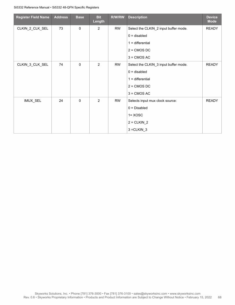
Register Field Name Address Base BitLength
R/W/RW Description DeviceMode
CLKIN_2_CLK_SEL 73 0 2 RW Select the CLKIN_2 input buffer mode.
0 = disabled
1 = differential
2 = CMOS DC
3 = CMOS AC
READY
CLKIN_3_CLK_SEL 74 0 2 RW Select the CLKIN_3 input buffer mode.
0 = disabled
1 = differential
2 = CMOS DC
3 = CMOS AC
READY
IMUX_SEL 24 0 2 RW Selects input mux clock source:
0 = Disabled
1= XOSC
2 = CLKIN_2
3 =CLKIN_3
READY
Si5332 Reference Manual • Si5332 48-QFN Specific Registers
Skyworks Solutions, Inc. • Phone [781] 376-3000 • Fax [781] 376-3100 • [email protected] • www.skyworksinc.com68 Rev. 0.6 • Skyworks Proprietary Information • Products and Product Information are Subject to Change Without Notice • February 15, 2022 68

Copyright © 2022 Skyworks Solutions, Inc. All Rights Reserved.
nformation in this document is provided in connection with Skyworks Solutions, Inc. (“Skyworks”) products or services. These materials, including the information contained herein, are provided by Skyworks as a service to its customers and may be used for informational purposes only by the customer. Skyworks assumes no responsibility for errors or omissions in these materials or the information contained herein. Skyworks may change its documentation, products, services, specifications or product descriptions at any time, without notice. Skyworks makes no commitment to update the materials or information and shall have no responsibility whatsoever for conflicts, incompatibilities, or other difficulties arising from any future changes.
No license, whether express, implied, by estoppel or otherwise, is granted to any intellectual property rights by this document. Skyworks assumes no liability for any materials, products or information provided hereunder, including the sale, distribution, reproduction or use of Skyworks products, information or materials, except as may be provided in Skyworks’ Terms and Conditions of Sale.
THE MATERIALS, PRODUCTS AND INFORMATION ARE PROVIDED “AS IS” WITHOUT WARRANTY OF ANY KIND, WHETHER EXPRESS, IMPLIED, STATUTORY, OR OTHERWISE, INCLUDING FITNESS FOR A PARTICULAR PURPOSE OR USE, MERCHANTABILITY, PERFORMANCE, QUALITY OR NON-INFRINGEMENT OF ANY INTELLECTUAL PROPERTY RIGHT; ALL SUCH WARRANTIES ARE HEREBY EXPRESSLY DISCLAIMED. SKYWORKS DOES NOT WARRANT THE ACCURACY OR COMPLETENESS OF THE INFORMATION, TEXT, GRAPHICS OR OTHER ITEMS CONTAINED WITHIN THESE MATERIALS. SKYWORKS SHALL NOT BE LIABLE FOR ANY DAMAGES, INCLUDING BUT NOT LIMITED TO ANY SPECIAL, INDIRECT, INCIDENTAL, STATUTORY, OR CONSEQUENTIAL DAMAGES, INCLUDING WITHOUT LIMITATION, LOST REVENUES OR LOST PROFITS THAT MAY RESULT FROM THE USE OF THE MATERIALS OR INFORMATION, WHETHER OR NOT THE RECIPIENT OF MATERIALS HAS BEEN ADVISED OF THE POSSIBILITY OF SUCH DAMAGE
Skyworks products are not intended for use in medical, lifesaving or life-sustaining applications, or other equipment in which the failure of the Skyworks products could lead to personal injury, death, physical or environmental damage. Skyworks customers using or selling Skyworks products for use in such applications do so at their own risk and agree to fully indemnify Skyworks for any damages resulting from such improper use or sale.
Customers are responsible for their products and applications using Skyworks products, which may deviate from published specifications as a result of design defects, errors, or operation of products outside of published parameters or design specifications. Customers should include design and operating safeguards to minimize these and other risks. Skyworks assumes no liability for applications assistance, customer product design, or damage to any equipment resulting from the use of Skyworks products outside of Skyworks’ published specifications or parameters.
Skyworks, the Skyworks symbol, Sky5®, SkyOne®, SkyBlue™, Skyworks Green™, Clockbuilder®, DSPLL®, ISOmodem®, ProSLIC®, and SiPHY® are trademarks or registered trademarks of Skyworks Solutions, Inc. or its subsidiaries in the United States and other countries. Third-party brands and names are for identification purposes only and are the property of their respective owners. Additional information, including relevant terms and conditions, posted at www.skyworksinc.com, are incorporated by reference.
Skyworks Solutions, Inc. | Nasdaq: SWKS | [email protected] | www.skyworksinc.com
USA: 781-376-3000 | Asia: 886-2-2735 0399 | Europe: 33 (0)1 43548540
Portfolio
skyworksinc.com
Quality
skyworksinc.com/quality
SW/HW
skyworksinc.com/CBPro
Support & Resources
skyworksinc.com/support
ClockBuilder ProOne-click access to Timing tools,
documentation, software, source
code libraries & more. Available for
Windows and iOS (CBGo only).
skyworksinc.com/CBPro