Embed Size (px)
Citation preview

FMC-SDF
DESCRIPTIONThe FMC-SDF module features four simultaneously sampling ADCs andDACs with an FPGA computing core. High resolution sigma-delta ADCs andhigh resolution DACs support high dynamic range applications such asaudio, ATE, and seismic data acquisition.
Clock and trigger controls include support for consistent servo loop timing,counted frames, software triggering and external triggering. The sample rateclock is either an external clock or on-board programmable PLL clock source
The FMC-SDF power consumption is 15 W for typical operation. The modulemay be conduction cooled using VITA20 standard and a heat spreadingplate. Ruggedization levels for wide-temperature operation are availablefrom -40 to +85C operation and 0.1 g2/Hz vibration. Conformal coating isalso available.
Support logic in VHDL is provided for integration with FPGA carrier cards.Specific support for Innovative carrier cards includes integration withFramework Logic tools that support VHDL and Matlab developers. TheMatlab BSP supports real-time hardware-in-the-loop development using thegraphical block diagram Simulink environment with Xilinx System Generatorfor the FMC integrated with the FPGA carrier card.
Software tools for Innovative carrier cards include host development C++libraries and drivers for Windows and Linux, 32/64-bit including RTOSvariants. Application examples demonstrating the module features areprovided.
* Sampling rates in an application depend on carrier and system design.
PRODUCTION DATA information is current as of publication date. Products conform to specifications per the terms of the Innovative Integration standard warranty. Production processing does not necessarilyinclude testing of all parameters.
02/14/17
FEATURES• Four A/D Input Channels
• ± 5V Input Range
• 625 kSPS, 24-bit A/D
• Differential
• Two D/A Output Channels
• 2.1μs Settling Time, 18-bit D/A
• ± 5V Output Range
• Tachometer Input
• Schmitt-Triggered for glitch tolerance
• Can be configured to operate differentially.
• Sample clocks and timing and controls
• 10 MHz, ±250 ppb stability on-board reference.
• Programmable PLL
• Programmable Clock Frequency as low as 3.05 kHz
• Integrated with FMC triggers
• FMC module, VITA 57.1
• High Pin Count no SERDES required
• Compatible with 2.5V VADJ
• Power monitor and controls
• 15 W typical
• Conduction Cooling per VITA 20 subset
• Environmental ratings for -40 to 85C 9g RMS sine, 0.1g2/Hz random vibration
APPLICATIONS• Seismic Data Acquisition
• Audio and Acoustic Testing
• ATE
• Other High SNR Data Acquisition
SOFTWARE• MATLAB/VHDL FrameWork Logic
Please be aware that an important notice concerning availability, standard warranty, and use in critical applications of Innovative Integration products and disclaimers thereto appears at the end of this data sheet. All trademarks are the property of their respective owners.
© 2017 Innovative Integration • phone 805.383.8994 • fax 805.482.8470 • www.innovative-dsp.com
FMC Module with four 24-bit, 625 kSPS A/D channels; two 18-bit D/A channels with on-board timing controls.
V 0.2 2/12/2017

FMC-SDF This electronics assembly can be damaged by ESD. Innovative Integration recommends that all electronic assemblies and components circuits be handled with appropriate precautions. Failure to observe proper handling and installation procedures can cause damage. ESD damage can range from subtle performance degradation to complete device failure. Precision integrated circuits may be more susceptible to damage because very small parametric changes could cause the device not to meet its published specifications.
ORDERING INFORMATIONProduct Part No. Description
FMC-SDF 80348-0-<ER> FMC module with four 24-bit A/Ds (625 kSPS per channel), two 18-bit DACs (2.1 μs settling time), on-board PLL.
<ER> is environmental rating L0...L4.
Cables
80350-1-L0
67227
Breakout module with all SMA connectors
Ribbon Coaxial Cable connecting FMC module to breakout module
Carrier Cards
VPX6-COP 80262 3U VPX FPGA co-processor card with FMC site
PEX6-COP 80284 Desktop/server PCI Express FPGA co-processor card with FMC site
Cardsharp 80332 Zynq-based Single Board Computer with HPC FMC IO Site
Embedded Computer Hosts
ePC-K7 90502 Embedded PC with support for one FMC module; COM Express Type 6 i7 CPU; RF expansion tray; Windows, Linux
Mini-K7 90600 Miniature embedded PC with support for one FMC module; COM Express Type 6 Atom CPU; RF expansion tray; LCD display; Windows, Linux
Innovative Integration • phone 805.383.8994 • fax 805.482.8470 • www.innovative-dsp.com 2 of 16

FMC-SDF
Innovative Integration • phone 805.383.8994 • fax 805.482.8470 • www.innovative-dsp.com 3 of 16
FMC Connector
AD9510
Out0
Out1
Out2Out3
Out4
Out5
Out6
Out7
CLK1
CLK2
REFIN
CSB
SCLK
SDIO
SDO
Status Fu
nctio
n
AD9508CLK
SDIO/SDA/S1
SCLK/SCL/S0
CS\ / S2
SYNC\
Out0
Out1
Out2
Out3
CP ADCLK_0
ADCLK_1
ADCLK_2
ADCLK_3
FMC_PLL_SYNC2FMC_PLL2_CS_N
FMC_PLL_SCLK
FMC_PLL_SDIO
CLK0_M2C_P/N
CLK1_M2C_P/N
FMC_DAC_LDAC_N
FMC_PLL1_CS_N
FMC_PLL_SYNC1
2:1 Mux
10 MHz XO
REF_SEL
2:1 Mux
EXT_CLK_SEL
CLK2_BIDIR_P/N
QSE Connector
CH0_P/N
CH1_P/N
CH2_P/N
CH3_P/N
DAC0
DAC1
TACH_P/N
EXT_CLK_P/N
EXT_TRIG_P/N
Signal FormatsAnalog/Generic
CMOS
LVDS
HSDS (6mA)
LVPECL
FMC_DAC_SCK
FMC_DAC_SDI
FMC_DAC_CS_N_LD
FMC_DAC_CLRN
FMC_DAC1_RFLAG_N
FMC_DAC1_SRO
I2V & LPF
LTC2758
SCK
SDI
CS\ / LD
CLR\
RFLAG\
LDAC\
SRO
IOUTA
IOUTB
AD7763
FSO\SCOSDO
DRDY
SDIFSI\
MCLKSYNC\
RESET\
VIN+
AD7763
FSO\SCOSDO
DRDY
SDIFSI\
MCLKSYNC\
RESET\
VIN+
AD7763
FSO\SCOSDO
DRDY
SDIFSI\
MCLKSYNC\
RESET\
VIN+/-
AD7763
FSO\SCOSDO
DRDY
SDIFSI\
MCLKSYNC\
RESET\
VIN+/-
FMC_ADC_SYNC_NFMC_ADC_RST_N
FMC_ADC0_SDIFMC_ADC0_FSI_NFMC_ADC0_DRDY
FMC_ADC0_SDOFMC_ADC0_SCO
FMC_ADC0_FSO_N
FMC_ADC1_SDIFMC_ADC1_FSI_NFMC_ADC1_DRDY
FMC_ADC1_SDOFMC_ADC1_SCO
FMC_ADC1_FSO_N
FMC_ADC2_SDIFMC_ADC2_FSI_NFMC_ADC2_DRDY
FMC_ADC2_SDOFMC_ADC2_SCO
FMC_ADC2_FSO_N
FMC_ADC3_SDIFMC_ADC3_FSI_NFMC_ADC3_DRDY
FMC_ADC3_SDOFMC_ADC3_SCO
FMC_ADC3_FSO_N
2:1 Mux
100-140 MHz VCO
Vt RFCLK3_BIDIR_P/N
FMC_TRIGOUT_P/N
TRIG_SEL
PG_C2MPG_M2C
FMC_SDAFMC_SCLFMC_G0FMC_G1
FMC_TEMP_ALERTFMC_TACH_P/N
TACH_P/N
FMC-SDF Detailed Block Diagram
FMC_PLL_STATUS1
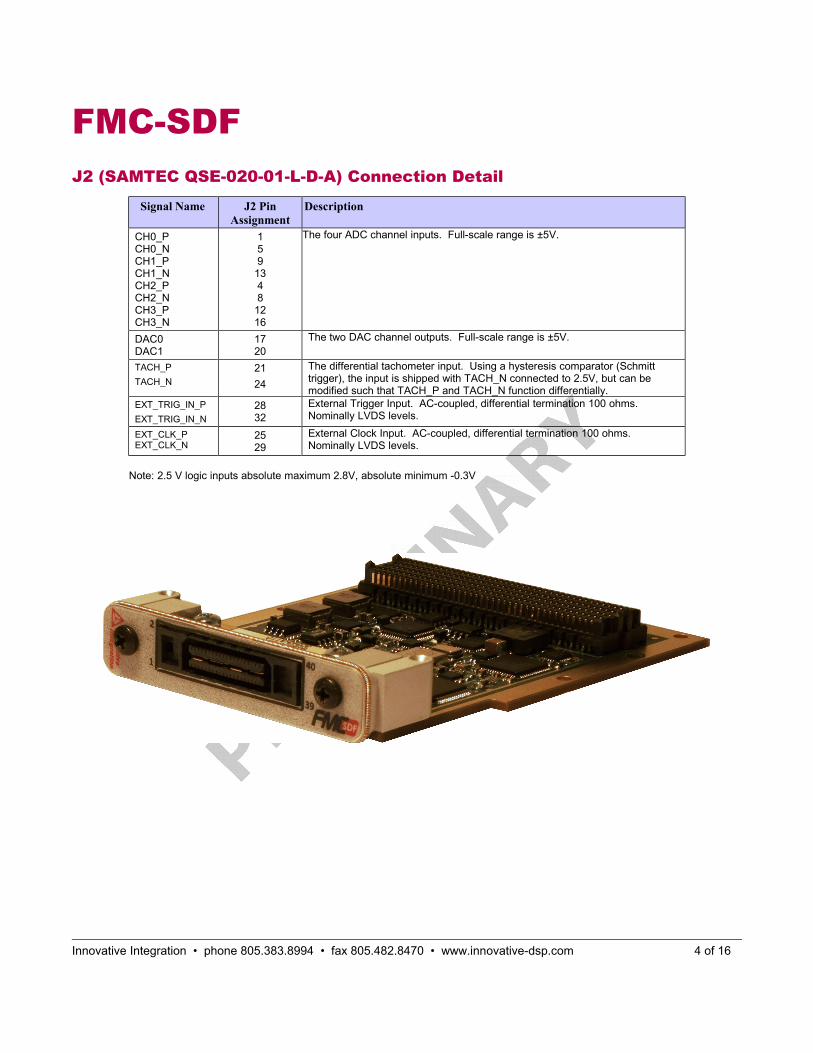
FMC-SDFJ2 (SAMTEC QSE-020-01-L-D-A) Connection Detail
Signal Name J2 PinAssignment
Description
CH0_PCH0_NCH1_PCH1_NCH2_PCH2_NCH3_PCH3_N
159
1348
1216
The four ADC channel inputs. Full-scale range is ±5V.
DAC0DAC1
1720
The two DAC channel outputs. Full-scale range is ±5V.
TACH_P
TACH_N
21
24
The differential tachometer input. Using a hysteresis comparator (Schmitt trigger), the input is shipped with TACH_N connected to 2.5V, but can be modified such that TACH_P and TACH_N function differentially.
EXT_TRIG_IN_P
EXT_TRIG_IN_N
2832
External Trigger Input. AC-coupled, differential termination 100 ohms.Nominally LVDS levels.
EXT_CLK_PEXT_CLK_N
2529
External Clock Input. AC-coupled, differential termination 100 ohms. Nominally LVDS levels.
Note: 2.5 V logic inputs absolute maximum 2.8V, absolute minimum -0.3V
Innovative Integration • phone 805.383.8994 • fax 805.482.8470 • www.innovative-dsp.com 4 of 16

FMC-SDFOperating Environment RatingsModules rated for operating environment temperature, shock and vibration are offered. The modules are qualified for wide temperature, vibration and shock to suit a variety of applications in each of the environmental ratings L0 through L4 and 100% tested for compliance.
Environment Rating <ER>
L0 L1 L2 L3 L4
Environment Office, controlled lab
Outdoor, stationary Industrial Vehicles Military and heavy industry
Applications Lab instruments, research
Outdoor monitoring and controls
Industrial applications with moderate vibration
Manned vehicles Unmanned vehicles, missiles, oil and gas exploration
Cooling Forced Air
2 CFM
Forced Air
2 CFM
Conduction Conduction Conduction
Operating Temperature 0 to +50C -40 to +85C -20 to +65C -40 to +70C -40 to +85C
Storage Temperature -20 to +90C -40 to +100C -40 to +100C -40 to +100C -50 to +100C
Vibration Sine - - 2g
20-500 Hz
5g
20-2000 Hz
10g
20-2000 Hz
Random - - 0.04 g2/Hz
20-2000 Hz
0.1 g2/Hz
20-2000 Hz
0.1 g2/Hz
20-2000 Hz
Shock - - 20g, 11 ms 30g, 11 ms 40g, 11 ms
Humidity 0 to 95%,
non-condensing
0 to 100% 0 to 100% 0 to 100% 0 to 100%
Conformal coating Conformal coating Conformal coating,
extended temperature range devices
Conformal coating,
extended temperature range devices,
Thermal conduction assembly
Conformal coating,
extended temperature range devices,
Thermal conduction assembly,
Epoxy bonding for devices
Testing Functional,
Temperature cycling
Functional,
Temperature cycling,
Wide temperature testing
Functional,
Temperature cycling,
Wide temperature testing
Vibration, Shock
Functional,
Temperature cycling,
Wide temperature testing
Vibration, Shock
Functional,
Testing per MIL-STD-810G for vibration, shock, temperature, humidity
Minimum lot sizes and NRE charges may apply. Contact sales support for pricing and availability.
Innovative Integration • phone 805.383.8994 • fax 805.482.8470 • www.innovative-dsp.com 5 of 16
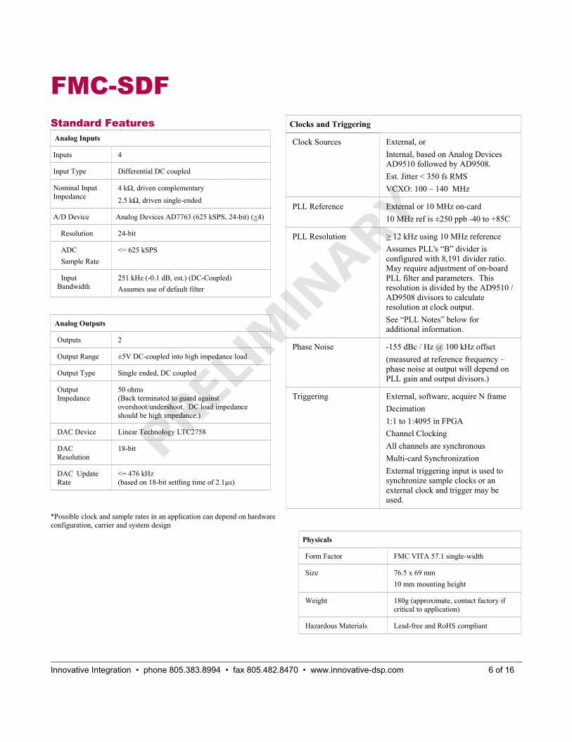
FMC-SDFStandard Features
Analog Inputs
Inputs 4
Input Type Differential DC coupled
Nominal Input Impedance
4 kΩ, driven complementary
2.5 kΩ, driven single-ended
A/D Device Analog Devices AD7763 (625 kSPS, 24-bit) (×4)
Resolution 24-bit
ADC
Sample Rate
<= 625 kSPS
Input Bandwidth
251 kHz (-0.1 dB, est.) (DC-Coupled)
Assumes use of default filter
Analog Outputs
Outputs 2
Output Range ±5V DC-coupled into high impedance load.
Output Type Single ended, DC coupled
Output Impedance
50 ohms (Back terminated to guard against overshoot/undershoot. DC load impedance should be high impedance.)
DAC Device Linear Technology LTC2758
DAC Resolution
18-bit
DAC Update Rate
<= 476 kHz (based on 18-bit settling time of 2.1µs)
*Possible clock and sample rates in an application can depend on hardware configuration, carrier and system design
Clocks and Triggering
Clock Sources External, or
Internal, based on Analog Devices AD9510 followed by AD9508.
Est. Jitter < 350 fs RMS
VCXO: 100 – 140 MHz
PLL Reference External or 10 MHz on-card
10 MHz ref is ±250 ppb -40 to +85C
PLL Resolution > 12 kHz using 10 MHz reference
Assumes PLL's “B” divider is configured with 8,191 divider ratio. May require adjustment of on-board PLL filter and parameters. This resolution is divided by the AD9510 /AD9508 divisors to calculate resolution at clock output.
See “PLL Notes” below for additional information.
Phase Noise -155 dBc / Hz @ 100 kHz offset
(measured at reference frequency – phase noise at output will depend on PLL gain and output divisors.)
Triggering External, software, acquire N frame
Decimation
1:1 to 1:4095 in FPGA
Channel Clocking
All channels are synchronous
Multi-card Synchronization
External triggering input is used to synchronize sample clocks or an external clock and trigger may be used.
Physicals
Form Factor FMC VITA 57.1 single-width
Size 76.5 x 69 mm
10 mm mounting height
Weight 180g (approximate, contact factory if critical to application)
Hazardous Materials Lead-free and RoHS compliant
Innovative Integration • phone 805.383.8994 • fax 805.482.8470 • www.innovative-dsp.com 6 of 16

FMC-SDFFMC Interface
IO LA[33:0] pairs, HA[22:0] pairs, HB[12:0] pairs
IO Standards LA: LVDS
HA: LVDSHB : LVCMOS 1.7V to 3.3V
Required voltages 3.3V, 12V
VADJ = 1.7 to 3.3 V
*Possible rates in an application can depend on hardware configuration, carrier and system design
Power
All DC coupled
Total 15.03 W
3.3V < 5.1 mA (< 17 mW)
12V 1250 mA (15 W)
2.5V Vadj
< 5.1 mA (< 13 mW)
Heat Sinking Conduction cooling supported, system level thermal design may be required
Innovative Integration • phone 805.383.8994 • fax 805.482.8470 • www.innovative-dsp.com 7 of 16
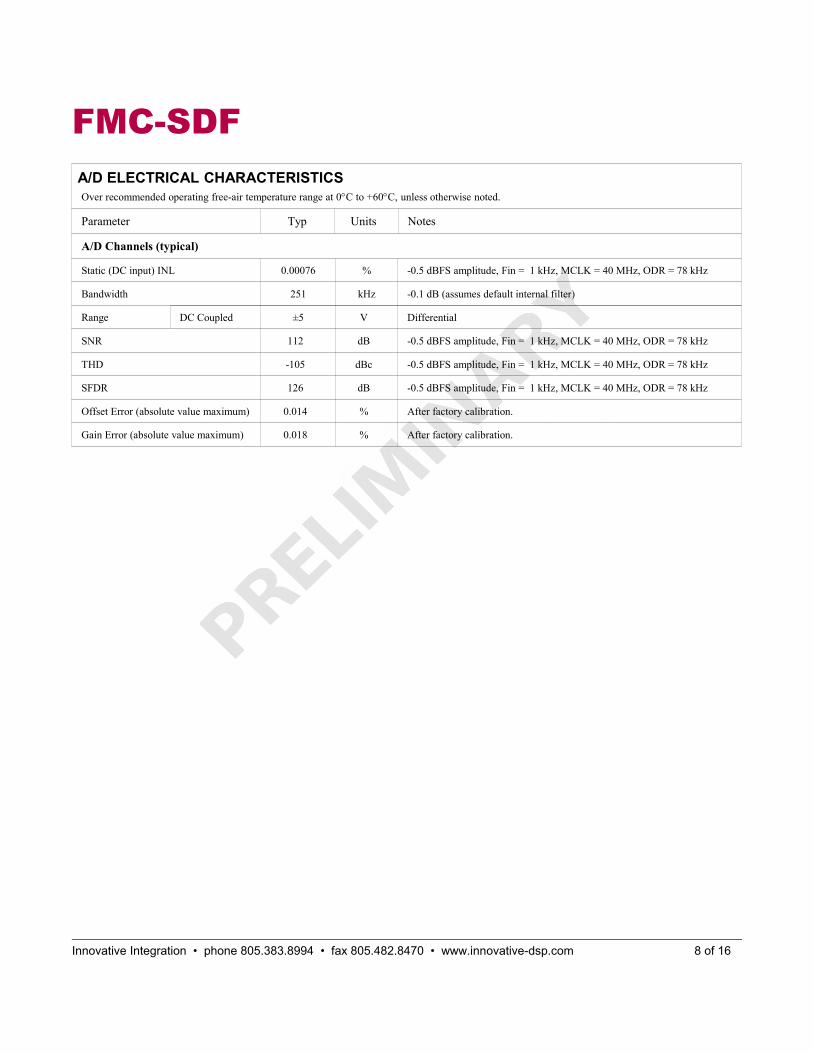
FMC-SDFA/D ELECTRICAL CHARACTERISTICSOver recommended operating free-air temperature range at 0C to +60C, unless otherwise noted.
Parameter Typ Units Notes
A/D Channels (typical)
Static (DC input) INL 0.00076 % -0.5 dBFS amplitude, Fin = 1 kHz, MCLK = 40 MHz, ODR = 78 kHz
Bandwidth 251 kHz -0.1 dB (assumes default internal filter)
Range DC Coupled ±5 V Differential
SNR 112 dB -0.5 dBFS amplitude, Fin = 1 kHz, MCLK = 40 MHz, ODR = 78 kHz
THD -105 dBc -0.5 dBFS amplitude, Fin = 1 kHz, MCLK = 40 MHz, ODR = 78 kHz
SFDR 126 dB -0.5 dBFS amplitude, Fin = 1 kHz, MCLK = 40 MHz, ODR = 78 kHz
Offset Error (absolute value maximum) 0.014 % After factory calibration.
Gain Error (absolute value maximum) 0.018 % After factory calibration.
Innovative Integration • phone 805.383.8994 • fax 805.482.8470 • www.innovative-dsp.com 8 of 16
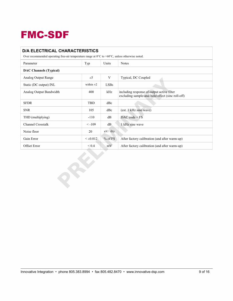
FMC-SDFD/A ELECTRICAL CHARACTERISTICSOver recommended operating free-air temperature range at 0C to +60C, unless otherwise noted.
Parameter Typ Units Notes
DAC Channels (Typical)
Analog Output Range ±5 V Typical, DC Coupled
Static (DC output) INL within ±2 LSBs
Analog Output Bandwidth 400 kHz including response of output active filterexcluding sample-and-hold effect (sinc roll-off)
SFDR TBD dBc
SNR 105 dBc (est. 1 kHz sine wave)
THD (multiplying) -110 dB DAC code = FS
Channel Crosstalk < -109 dB 1 kHz sine wave
Noise floor 20 nV/ √Hz
Gain Error < ±0.012 % of FS After factory calibration (and after warm-up)
Offset Error < 0.4 mV After factory calibration (and after warm-up)
Innovative Integration • phone 805.383.8994 • fax 805.482.8470 • www.innovative-dsp.com 9 of 16

FMC-SDFNotes
Digital Calibration Note
The FMC-SDF can be digitally calibrated for offset and gain. However if the signal is clipped (outside the A/D range) theinformation is lost, so the raw gain is typically designed for a signal level at the A/D that is slightly less than A/D Full Scalein the bandwidth of interest to allow the nominal input range to be measured accurately without clipping when digitallycalibrated.
PLL Notes
The serial clock for the ADCs (MCLK) is produced by an integer division (1~32) of the VCO output generated by theAD9510. The VCO has a tuning range of 100 – 140 MHz. This tuning range limits the range of frequencies that can beproduced by integer division. For output clock frequencies below 46.67 MHz (140 MHz / 3) some combination of VCOfrequency and division ratio can be chosen to produce any arbitrary output clock frequency because the various divideroutput frequency ranges overlap. The AD9510 is capable of producing a wide range of frequencies based on the option touse a dual modulus N counter. If the dual modulus option is avoided, however, the available frequencies may also limited bythe acceptable values for N and R (since large values of N and R may increase phase noise, or may even render the synthesisloop unstable). For example MCLK = 40 MHz can be synthesized with a VCO frequency of 120 MHz (N = 3, R= 1) but afrequency of 40.0075 MHz requires a VCO frequency of 120.0225 MHz (N = 48009, R = 4000). Accordingly, the range offrequencies available for MCLK is 5.185 – 46.667 MHz (keeping in mind the AD7763 has a maximum MCLK rate of 40MHz).
As designed, the serial clock for the DAC is provided through the FMC interface (FMC_DAC_SCK), but the update clock(LDAC\) is generated by a combination of the AD9510 output followed by an additional divider. Accordingly, the updaterate can be set to any frequency ranging between 3.05 kHz and 486.11 kHz (although the maximum update rate is still limitedby the 2.1µs settling time). A list of available clock rates is shown in Table 1.
Table 1. Range of output clock frequencies showing continuous coverage in the tuning range.
Innovative Integration • phone 805.383.8994 • fax 805.482.8470 • www.innovative-dsp.com 10 of 16
AD9508 Div
AD9510Div Fmin Fmax
1024 3 - 32 3.05 kHz 45.57 kHz96 3 - 32 45.57 kHz 486.11 kHz9 3 - 32 486.11 kHz 5.185 MHz1 3 - 32 5.185 MHz 46.667 MHz

FMC-SDFFMC Connector Pin Assignments
Innovative Integration • phone 805.383.8994 • fax 805.482.8470 • www.innovative-dsp.com 11 of 16
P1 P1 Pin FMC-SDFPins Name NetA1 GND GND
A2 DP1_M2C_P N/C
A3 DP1_M2C_N N/C
A4 GND GND
A5 GND GND
A6 DP2_M2C_P N/C
A7 DP2_M2C_N N/C
A8 GND GND
A9 GND GND
A10 DP3_M2C_P N/C
A11 DP3_M2C_N N/C
A12 GND GND
A13 GND GND
A14 DP4_M2C_P N/C
A15 DP4_M2C_N N/C
A16 GND GND
A17 GND GND
A18 DP5_M2C_P N/C
A19 DP5_M2C_N N/C
A20 GND GND
A21 GND GND
A22 DP1_C2M_P N/C
A23 DP1_C2M_N N/C
A24 GND GND
A25 GND GND
A26 DP2_C2M_P N/C
A27 DP2_C2M_N N/C
A28 GND GND
A29 GND GND
A30 DP3_C2M_P N/C
A31 DP3_C2M_N N/C
A32 GND GND
A33 GND GND
A34 DP4_C2M_P N/C
A35 DP4_C2M_N N/C
A36 GND GND
A37 GND GND
A38 DP5_C2M_P N/C
A39 DP5_C2M_N N/C
A40 GND GND
B1 CLK_DIR 3P3V
B2 GND GND
B3 GND GND
B4 DP9_M2C_P N/C
B5 DP9_M2C_N N/C
B6 GND GND
B7 GND GND
B8 DP8_M2C_P N/C
B9 DP8_M2C_N N/C
B10 GND GND
B11 GND GND
B12 DP7_M2C_P N/C
B13 DP7_M2C_N N/C
B14 GND GND
B15 GND GND
B16 DP6_M2C_P N/C
B17 DP6_M2C_N N/C
B18 GND GND
B19 GND GND
B20 GBTCLK1_M2C_P N/C
B21 GBTCLK1_M2C_N N/C
B22 GND GND
B23 GND GND
B24 DP9_C2M_P N/C
B25 DP9_C2M_N N/C
B26 GND GND
B27 GND GND
B28 DP8_C2M_P N/C
B29 DP8_C2M_N N/C
B30 GND GND
B31 GND GND
B32 DP7_C2M_P N/C
B33 DP7_C2M_N N/C
B34 GND GND
B35 GND GND
B36 DP6_C2M_P N/C
B37 DP6_C2M_N N/C
B38 GND GND
B39 GND GND
B40 RES0 N/C

FMC-SDFFMC Connector Pin Assignments (cont.)
Innovative Integration • phone 805.383.8994 • fax 805.482.8470 • www.innovative-dsp.com 12 of 16
C1 GND GND
C2 DP0_C2M_P N/C
C3 DP0_C2M_N N/C
C4 GND GND
C5 GND GND
C6 DP0_M2C_P N/C
C7 DP0_M2C_N N/C
C8 GND GND
C9 GND GND
C10 LA06_P FMC_DAC_SCK
C11 LA06_N FMC_DAC_SDI
C12 GND GND
C13 GND GND
C14 LA10_P FMC_DAC_CSN_LD
C15 LA10_N FMC_DAC_CLRN
C16 GND GND
C17 GND GND
C18 LA14_P FMC_DAC1_SRO
C19 LA14_N FMC_DAC1_RFLAGN
C20 GND GND
C21 GND GND
C22 LA18_P_CC FMC_TACH_OUT_P
C23 LA18_N_CC FMC_TACH_OUT_N
C24 GND GND
C25 GND GND
C26 LA27_P FMC_DAC1_LDAC
C27 LA27_N N/C
C28 GND GND
C29 GND GND
C30 SCL FMC_SCL
C31 SDA FMC_SDA
C32 GND GND
C33 GND GND
C34 GA0 FMC_G0
C35 12P0V 12P0V
C36 GND GND
C37 12P0V 12P0V
C38 GND GND
C39 3P3V 3P3V
C40 GND GND
D1 PG_C2M FMC_PG_C2M
D2 GND GND
D3 GND GND
D4 GBTCLK0_M2C_P N/C
D5 GBTCLK0_M2C_N N/C
D6 GND GND
D7 GND GND
D8 LA01_P_CC N/C
D9 LA01_N_CC N/C
D10 GND GND
D11 LA05_P N/C
D12 LA05_N N/C
D13 GND GND
D14 LA09_P N/C
D15 LA09_N N/C
D16 GND GND
D17 LA13_P N/C
D18 LA13_N N/C
D19 GND GND
D20 LA17_P_CC N/C
D21 LA17_N_CC N/C
D22 GND GND
D23 LA23_P N/C
D24 LA23_N N/C
D25 GND GND
D26 LA26_P N/C
D27 LA26_N N/C
D28 GND GND
D29 TCK N/C
D30 TDI N/C
D31 TDO N/C
D32 3P3VAUX 3P3V_AUX
D33 TMS N/C
D34 TRST_L N/C
D35 GA1 FMC_G1
D36 3P3V 3P3V
D37 GND GND
D38 3P3V 3P3V
D39 GND GND
D40 3P3V 3P3V

FMC-SDFFMC Connector Pin Assignments (cont.)
Innovative Integration • phone 805.383.8994 • fax 805.482.8470 • www.innovative-dsp.com 13 of 16
E1 GND GND
E2 HA01_P_CC N/C
E3 HA01_N_CC N/C
E4 GND GND
E5 GND GND
E6 HA05_P N/C
E7 HA05_N N/C
E8 GND GND
E9 HA09_P N/C
E10 HA09_N N/C
E11 GND GND
E12 HA13_P N/C
E13 HA13_N N/C
E14 GND GND
E15 HA16_P N/C
E16 HA16_N N/C
E17 GND GND
E18 HA20_P N/C
E19 HA20_N N/C
E20 GND GND
E21 HB03_P N/C
E22 HB03_N N/C
E23 GND GND
E24 HB05_P N/C
E25 HB05_N N/C
E26 GND GND
E27 HB09_P N/C
E28 HB09_N N/C
E29 GND GND
E30 HB13_P N/C
E31 HB13_N N/C
E32 GND GND
E33 HB19_P N/C
E34 HB19_N N/C
E35 GND GND
E36 HB21_P N/C
E37 HB21_N N/C
E38 GND GND
E39 VADJ VADJ
E40 GND GND
F1 PG_M2C PG_M2C
F2 GND GND
F3 GND GND
F4 HA00_P_CC N/C
F5 HA00_N_CC N/C
F6 GND GND
F7 HA04_P N/C
F8 HA04_N N/C
F9 GND GND
F10 HA08_P N/C
F11 HA08_N N/C
F12 GND GND
F13 HA12_P N/C
F14 HA12_N N/C
F15 GND GND
F16 HA15_P N/C
F17 HA15_N N/C
F18 GND GND
F19 HA19_P N/C
F20 HA19_N N/C
F21 GND GND
F22 HB02_P N/C
F23 HB02_N N/C
F24 GND GND
F25 HB04_P N/C
F26 HB04_N N/C
F27 GND GND
F28 HB08_P N/C
F29 HB08_N N/C
F30 GND GND
F31 HB12_P N/C
F32 HB12_N N/C
F33 GND GND
F34 HB16_P N/C
F35 HB16_N N/C
F36 GND GND
F37 HB20_P N/C
F38 HB20_N N/C
F39 GND GND
F40 VADJ VADJ
FMC-SDFFMC Connector Pin Assignments (cont.)
Innovative Integration • phone 805.383.8994 • fax 805.482.8470 • www.innovative-dsp.com 14 of 16
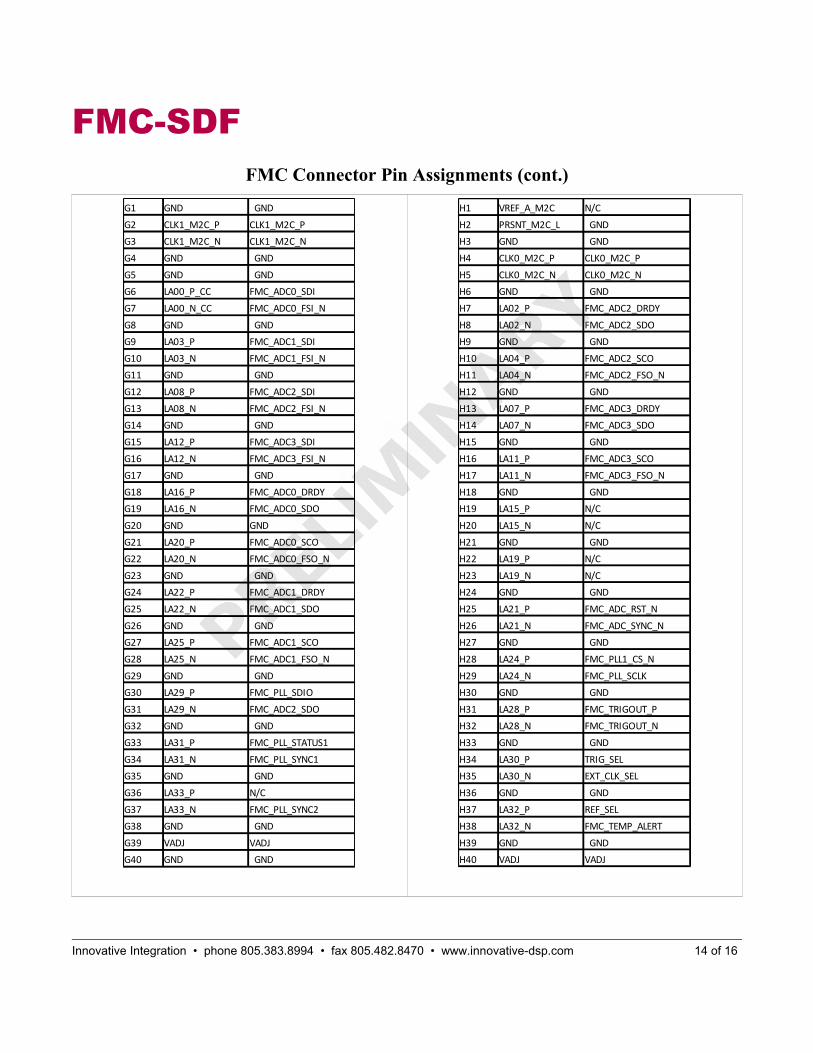
G1 GND GND
G2 CLK1_M2C_P CLK1_M2C_P
G3 CLK1_M2C_N CLK1_M2C_N
G4 GND GND
G5 GND GND
G6 LA00_P_CC FMC_ADC0_SDI
G7 LA00_N_CC FMC_ADC0_FSI_N
G8 GND GND
G9 LA03_P FMC_ADC1_SDI
G10 LA03_N FMC_ADC1_FSI_N
G11 GND GND
G12 LA08_P FMC_ADC2_SDI
G13 LA08_N FMC_ADC2_FSI_N
G14 GND GND
G15 LA12_P FMC_ADC3_SDI
G16 LA12_N FMC_ADC3_FSI_N
G17 GND GND
G18 LA16_P FMC_ADC0_DRDY
G19 LA16_N FMC_ADC0_SDO
G20 GND GND
G21 LA20_P FMC_ADC0_SCO
G22 LA20_N FMC_ADC0_FSO_N
G23 GND GND
G24 LA22_P FMC_ADC1_DRDY
G25 LA22_N FMC_ADC1_SDO
G26 GND GND
G27 LA25_P FMC_ADC1_SCO
G28 LA25_N FMC_ADC1_FSO_N
G29 GND GND
G30 LA29_P FMC_PLL_SDIO
G31 LA29_N FMC_ADC2_SDO
G32 GND GND
G33 LA31_P FMC_PLL_STATUS1
G34 LA31_N FMC_PLL_SYNC1
G35 GND GND
G36 LA33_P N/C
G37 LA33_N FMC_PLL_SYNC2
G38 GND GND
G39 VADJ VADJ
G40 GND GND
H1 VREF_A_M2C N/C
H2 PRSNT_M2C_L GND
H3 GND GND
H4 CLK0_M2C_P CLK0_M2C_P
H5 CLK0_M2C_N CLK0_M2C_N
H6 GND GND
H7 LA02_P FMC_ADC2_DRDY
H8 LA02_N FMC_ADC2_SDO
H9 GND GND
H10 LA04_P FMC_ADC2_SCO
H11 LA04_N FMC_ADC2_FSO_N
H12 GND GND
H13 LA07_P FMC_ADC3_DRDY
H14 LA07_N FMC_ADC3_SDO
H15 GND GND
H16 LA11_P FMC_ADC3_SCO
H17 LA11_N FMC_ADC3_FSO_N
H18 GND GND
H19 LA15_P N/C
H20 LA15_N N/C
H21 GND GND
H22 LA19_P N/C
H23 LA19_N N/C
H24 GND GND
H25 LA21_P FMC_ADC_RST_N
H26 LA21_N FMC_ADC_SYNC_N
H27 GND GND
H28 LA24_P FMC_PLL1_CS_N
H29 LA24_N FMC_PLL_SCLK
H30 GND GND
H31 LA28_P FMC_TRIGOUT_P
H32 LA28_N FMC_TRIGOUT_N
H33 GND GND
H34 LA30_P TRIG_SEL
H35 LA30_N EXT_CLK_SEL
H36 GND GND
H37 LA32_P REF_SEL
H38 LA32_N FMC_TEMP_ALERT
H39 GND GND
H40 VADJ VADJ

FMC-SDFFMC Connector Pin Assignments (cont.)
Innovative Integration • phone 805.383.8994 • fax 805.482.8470 • www.innovative-dsp.com 15 of 16
J1 GND GND
J2 CLK3_BIDIR_P CLK3_BIDIR_P
J3 CLK3_BIDIR_N CLK3_BIDIR_N
J4 GND GND
J5 GND GND
J6 HA03_P N/C
J7 HA03_N N/C
J8 GND GND
J9 HA07_P N/C
J10 HA07_N N/C
J11 GND GND
J12 HA11_P N/C
J13 HA11_N N/C
J14 GND GND
J15 HA14_P N/C
J16 HA14_N N/C
J17 GND GND
J18 HA18_P N/C
J19 HA18_N N/C
J20 GND GND
J21 HA22_P N/C
J22 HA22_N N/C
J23 GND GND
J24 HB01_P N/C
J25 HB01_N N/C
J26 GND GND
J27 HB07_P N/C
J28 HB07_N N/C
J29 GND GND
J30 HB11_P N/C
J31 HB11_N N/C
J32 GND GND
J33 HB15_P N/C
J34 HB15_N N/C
J35 GND GND
J36 HB18_P N/C
J37 HB18_N N/C
J38 GND GND
J39 VIO_B_M2C N/C
J40 GND GND
K1 VREF_B_M2C N/C
K2 GND GND
K3 GND GND
K4 CLK2_BIDIR_P CLK2_BIDIR_P
K5 CLK2_BIDIR_N CLK2_BIDIR_N
K6 GND GND
K7 HA02_P N/C
K8 HA02_N N/C
K9 GND GND
K10 HA06_P N/C
K11 HA06_N N/C
K12 GND GND
K13 HA10_P N/C
K14 HA10_N N/C
K15 GND GND
K16 HA17_P_CC N/C
K17 HA17_N_CC N/C
K18 GND GND
K19 HA21_P N/C
K20 HA21_N N/C
K21 GND GND
K22 HA23_P N/C
K23 HA23_N N/C
K24 GND GND
K25 HB00_P_CC N/C
K26 HB00_N_CC N/C
K27 GND GND
K28 HB06_P_CC N/C
K29 HB06_N_CC N/C
K30 GND GND
K31 HB10_P N/C
K32 HB10_N N/C
K33 GND GND
K34 HB14_P N/C
K35 HB14_N N/C
K36 GND GND
K37 HB17_P_CC N/C
K38 HB17_N_CC N/C
K39 GND GND
K40 VIO_B_M2C VADJ

FMC-SDFIMPORTANT NOTICESInnovative Integration Incorporated reserves the right to make corrections, modifications, enhancements, improvements, andother changes to its products and services at any time and to discontinue any product or service without notice. Customersshould obtain the latest relevant information before placing orders and should verify that such information is current andcomplete. All products are sold subject to Innovative Integration’s terms and conditions of sale supplied at the time of orderacknowledgment.
Innovative Integration warrants performance of its hardware products to the specifications applicable at the time of sale inaccordance with Innovative Integration’s standard warranty. Testing and other quality control techniques are used to theextent Innovative Integration deems necessary to support this warranty. Except where mandated by governmentrequirements, testing of all parameters of each product is not necessarily performed.
Innovative Integration assumes no liability for applications assistance or customer product design. Customers are responsiblefor their products and applications using Innovative Integration products. To minimize the risks associated with customerproducts and applications, customers should provide adequate design and operating safeguards.
Innovative Integration does not warrant or represent that any license, either express or implied, is granted under anyInnovative Integration patent right, copyright, mask work right, or other Innovative Integration intellectual property rightrelating to any combination, machine, or process in which Innovative Integration products or services are used. Informationpublished by Innovative Integration regarding third-party products or services does not constitute a license from InnovativeIntegration to use such products or services or a warranty or endorsement thereof. Use of such information may require alicense from a third party under the patents or other intellectual property of the third party, or a license from InnovativeIntegration under the patents or other intellectual property of Innovative Integration.
Reproduction of information in Innovative Integration data sheets is permissible only if reproduction is without alteration andis accompanied by all associated warranties, conditions, limitations, and notices. Reproduction of this information withalteration is an unfair and deceptive business practice.
Innovative Integration is not responsible or liable for such altered documentation. Resale of Innovative Integration productsor services with statements different from or beyond the parameters stated by Innovative Integration for that product orservice voids all express and any implied warranties for the associated Innovative Integration product or service and is anunfair and deceptive business practice. Innovative Integration is not responsible or liable for any such statements.
For further information on Innovative Integration products and support see our web site:
www.innovative-dsp.com
Mailing Address: Innovative Integration, Inc.
741 Flynn Road, Camarillo, California 93012
Copyright © 2017, Innovative Integration, Incorporated
Innovative Integration • phone 805.383.8994 • fax 805.482.8470 • www.innovative-dsp.com 16 of 16