Embed Size (px)
Citation preview
Cronfa - Swansea University Open Access Repository
_____________________________________________________________
This is an author produced version of a paper published in :
ACS Applied Materials & Interfaces
Cronfa URL for this paper:
http://cronfa.swan.ac.uk/Record/cronfa29930
_____________________________________________________________
Paper:
Kryvchenkova, O., Abdullah, I., Macdonald, J., Elliott, M., Anthopoulos, T., Lin, Y., Igi, P., Kalna, K. & Cobley, R.
(2016). Nondestructive Method for Mapping Metal Contact Diffusion in In2O3Thin-Film Transistors. ACS Applied
Materials & Interfaces, 8(38), 25631-25636.
http://dx.doi.org/10.1021/acsami.6b10332
_____________________________________________________________ This article is brought to you by Swansea University. Any person downloading material is agreeing to abide by the
terms of the repository licence. Authors are personally responsible for adhering to publisher restrictions or conditions.
When uploading content they are required to comply with their publisher agreement and the SHERPA RoMEO
database to judge whether or not it is copyright safe to add this version of the paper to this repository.
http://www.swansea.ac.uk/iss/researchsupport/cronfa-support/

Nondestructive Method for Mapping Metal Contact Diffusion inIn2O3 Thin-Film TransistorsOlga Kryvchenkova,*,† Isam Abdullah,‡ John Emyr Macdonald,‡ Martin Elliott,‡
Thomas D. Anthopoulos,§ Yen-Hung Lin,§ Petar Igic,† Karol Kalna,† and Richard J. Cobley†
†Electronic Systems Design Centre, Swansea University, Swansea SA1 8EN, U.K.‡School of Physics and Astronomy, Cardiff University, The Parade, Cardiff CF24 3AA, U.K.§Department of Physics and Centre for Plastic Electronics, Blackett Laboratory, Imperial College London, London SW7 2AZ, U.K.
*S Supporting Information
ABSTRACT: The channel width-to-length ratio is animportant transistor parameter for integrated circuit design.Contact diffusion into the channel during fabrication oroperation alters the channel width and this importantparameter. A novel methodology combining atomic forcemicroscopy and scanning Kelvin probe microscopy (SKPM)with self-consistent modeling is developed for the non-destructive detection of contact diffusion on active devices.Scans of the surface potential are modeled using physicallybased Technology Computer Aided Design (TCAD) simu-lations when the transistor terminals are grounded and underbiased conditions. The simulations also incorporate the tip geometry to investigate its effect on the measurements due toelectrostatic tip−sample interactions. The method is particularly useful for semiconductor− and metal−semiconductor interfaceswhere the potential contrast resulting from dopant diffusion is below that usually detectable with scanning probe microscopy.
KEYWORDS: AFM, Kelvin probe, In2O3, solution processing, metal oxide transistors
1. INTRODUCTION
Atomic force microscopy (AFM) is a commonly used methodfor nondestructive mapping of sample topography1 and is alsoan essential part of the commonly used double-pass scanningKelvin probe microscopy (SKPM) method that allowsmeasurement of the sample surface potential.2−5 Using theknown tip work function, a 2D map of the sample surface workfunction can then be reconstructed.1−3 Measurements of thesurface potential on operating transistors are complicated bymobile charges which are continuously created and transportedacross the device6 and are influenced by the external field of themeasuring probes. Therefore, the measurement result willinclude not only the intrinsic electrical properties of the samplebut also measurement artifacts due to the presence of thetip.6−10 This characterization technique is applied here toinvestigate In2O3 thin-film transistors (TFTs).11−15
SKPM is a well-established technique to study deviceinterfaces.16 Diffusion at the interface gives rise to nonabruptpotential distributions which can be used to assess the effect.Several authors have studied similar dopant diffusion problemswith unbiased devices and structures, where potential offsets inthe region of 100s of mV are detectable.17,18 Here we focus onthe detection of diffusion at a device interface which gives riseto low potential changes, which are difficult to detect withSKPM on unbiased samples.
In2O3 is a wide bandgap material with a cubic crystalstructure.19,20 The thin-film form has high transparency in thevisible range (>90%), high electrical conductivity, and large-area uniformity. In2O3 is popular for potential deviceapplications including liquid crystal displays, solar cells, andresistive memories.11−14 In2O3 TFTs have also been proposedfor high-resolution displays where it is preferable to have a largeon-current to drive pixels and a low off-current for low powerconsumption. In2O3 TFTs on SiO2/Si substrates and Alelectrodes are typically bottom gate, normally on n-channeltransistors15 with a carrier mobility in the range from 0.4 to 23cm2/V·s and on−off ratio of ∼105−106.13,21−23 Al contacts arecommonly used due to the electrical properties and cost, whichgive reliable, time-stable contacts.24 One of the majordrawbacks in using Al contacts is the formation of the nativeoxide and Al diffusion into the semiconductor material whichcan affect the contact reliability.24−26
In this paper we first present a method for using SKPM andAFM to determine diffusion regions in In2O3 TFTs, which giverise to potential shifts close to the detection threshold forstandard AFM and SKPM. By applying a bias to the device, theunequal distribution of the applied potential between the
Received: August 17, 2016Accepted: September 1, 2016Published: September 1, 2016
Research Article
www.acsami.org
© 2016 American Chemical Society 25631 DOI: 10.1021/acsami.6b10332ACS Appl. Mater. Interfaces 2016, 8, 25631−25636
This is an open access article published under a Creative Commons Attribution (CC-BY)License, which permits unrestricted use, distribution and reproduction in any medium,provided the author and source are cited.

differently doped regions accentuates the difference, making thepotential change easily detectable. We then explore the effectsof gate bias and the interaction of the probe on this method.We investigate these effects and propose the most accuratemethod to nondestructively determine contact diffusion. Weverify our results using 2D drift-diffusion simulations in SilvacoAtlas.27 The diffusion alters the length of the channel, a crucialdesign parameter in transistor design, and is the cause of thehigher output current observed in devices with a large contactdiffusion area.
2. METHODS2.1. Transistor Fabrication. A schematic of the bottom-gate
In2O3 TFT operating under gate bias VGS > 0 and drain bias VDS > 0 isshown in Figure 1. The device has an aluminum source and drain
electrodes, a 100 nm thick SiO2 dielectric layer, an In2O3semiconducting channel layer, and a heavily doped n-type Si substratelayer, which serves as a gate electrode. The excessive indium atoms oroxygen vacancies serve as donors and make In2O3 an n-typesemiconductor.12,28 When positive drain voltages are applied, negativecharge from the source electrode is injected, and an n-type conductingchannel will be formed at the interface of the In2O3 layer with the SiO2gate dielectric, as shown in Figure 1(b).Two In2O3 TFTs were selected for direct comparison. Figure 2
shows the I−V characteristics of a single-spin TFT, for which a 4 nmIn2O3 film results from a single spin-casting procedure.22 The channellength L ∼ 30 μm, and width W ∼ 1000 μm. Figure 3 shows thecorresponding I−V characteristics for a film of thickness of 7−8 nmprepared by consecutive spin-casting of two layers of In2O3.
22 For thisdouble-spin device, L∼ 40 μm and W ∼ 200 μm. From the transfercharacteristic of the double-spin device shown in Figure 3(b) onecould estimate a threshold voltage value of 0.0 V, while the single-spindevice threshold voltage could be estimated at 2.5 V29,30 (see Figure2(b)).
2.2. SKPM and AFM Measurement Methods. A double-passSKPM method was performed on the In2O3 TFT in two stages, shownin Figure 1(a). During the first scan, surface topography is obtained inintermittent contact mode,2,31 during which the cantilever vibrationamplitude h1 is maintained by a feedback loop.1 An example of thereconstructed sample topography gradient for the single-spin device isshown in Figure 1(a) where source and drain electrodes can be clearlydetected. To obtain the surface potential VS in the second scan the tipis retracted at the constant lift height H = 20 nm (Figure 1(b)). Itfollows the line topography obtained in the first scan with theamplitude h2, where h2 < h1. During the second scan a constant voltageVDC + VAC sin(ωt) is applied to the tip with VDC varied to minimizethe amplitude of induced tip oscillations, so that the electrical potentialin the channel can be measured (after correction for the contactpotential difference between the tip and surface).1,32,33 During themeasurements the source electrode is always grounded. WSxM
Figure 1. Combined measurement-schematic illustration of the SKPMdouble-pass method performed on a typical n-channel In2O3 TFTstructure. (a) A 40 μm × 40 μm measured gradient map of the single-spin In2O3 TFT without bias and (b) the same at VDS = 5 V and VGS =0 V revealing the position of the diffusion region as marked, with aschematic of the device structure below.
Figure 2. (a) Output characteristic at VGS = 1 to 10 V with a step of 1V. (b) Transfer characteristics in the saturation regime at VDS = 10 Vfor the single-spin device.
Figure 3. (a) Output characteristic at VGS = 1 to 10 V with a step of 1V. (b) Transfer characteristics in the saturation regime at VDS = 10 Vfor the double spin device.
ACS Applied Materials & Interfaces Research Article
DOI: 10.1021/acsami.6b10332ACS Appl. Mater. Interfaces 2016, 8, 25631−25636
25632

software is used to visualize the 2D measured AFM and SKPMprofiles.34
2.3. Simulation Setup. The device structure shown in Figure 1(b)was modeled within Silvaco Atlas27 which has been used by us tomodel coupled device-probe measurements under device operation.35
In simulations, gate lengths of 25.62 μm (single spin) and 36.5 μm(double spin) are used with 70 μm Al source and drain electrodes, 4nm (single spin) and 10 nm (double spin) n-type In2O3-conductingchannel layer with a doping concentration of 8 × 1017 cm−3, 100 nmSiO2 insulator layer, and 300 nm n-type Si substrate layer with adoping concentration of 1020 cm−3 followed by a bottom Al gate. Tosimulate the contact diffusion regions around the drain and sourceelectrodes, we use an n-type doping concentration of 2 × 1018 cm−3.Other material parameters used in the simulations are In2O3permittivity of 8.9,36 bandgap of 4.0 eV,11,12,20,28 electron affinity of4.45 eV,11 field-effect mobility of 0.27 cm2/V × s, electron effectivemass of 0.3m0
20, and tip work function of 4.6 eV. The Schottky barrierheight of 0.7 eV is extracted from the measured profiles for the sourceand drain electrodes. The simulated devices have threshold voltages of−0.3 V for the double-spin transistor and 1.8 V for the single-spintransistor which is in good agreement with the measurements.The structural quality of the interface between the In2O3 channel
and dielectric material must be high to reduce scattering at theinterface.15 Charge-trapping effects in the channel layer have beenreported to result in a decrease in the drain current when the drainbias is further increased.15 In the present work, no current degradationis observed, and hence no charge-trapping effects are included in thesimulation.
3. RESULTS AND DISCUSSION
3.1. Single-Spin Device. Figure 4(a) shows that thesurface potential map at VGS = VDS = 0 V is flat and uniformthrough the channel with the averaged line scan shown beneathin Figure 4(b) where source and drain electrode edges can beseen at around 8 and 33 μm, respectively.In Figure 4(b), the potential distribution through the In2O3
channel at VDS = 5 V flattens in the region from 28 μm up untilthe previously determined edge of the drain electrode at 33 μm,in both the simulations and the experiment. Potential flatteningsuggests that this area is well-connected to the drain electrodeby a low resistance path, consistent with a higher dopingconcentration after Al diffusion into the In2O3 channel.Simulations suggest that the doping concentration in thediffusion region increased from 2 × 1017 cm−3 to 8 × 1018 cm−3.The edge of the diffusion region was estimated at 28.0 μmwhere the gradient of the surface lateral electric field (Figure4(c)), calculated as a second derivative of the potential, has alocal extremum. Analogously, using the data in Figure 4(b), theelectrode edges at 7.7 and 33.3 μm were detected where theabsolute change in the electric field has a local extremum. Thisgives a lateral diffusion width of 5.3 μm. Both profiles at VDS =0 V and VDS = 5 V are in a very good agreement and give thesame value of the electrode’s edge position.The position of the diffusion region edge can be determined
only from the potential profiles of the biased device. It wouldnot be possible to determine the diffusion region edge using thepotential profile when TFT terminals are grounded (VGS = VDS= 0 V) in Figure 4(b) because the surface potential change willonly depend on the intrinsic material parameters, In2O3 affinityof the channel layer, diffusion region, and Al work function.The potential drop between the In2O3 channel layer (with anestimated n-type doping concentration of 8 × 1017 cm−3) andIn2O3 diffusion region (with an estimated n-type dopingconcentration of 2 × 1018 cm−3) is only 0.028 V as derived fromthe simulation results. This potential drop of 0.028 eV is below
the practical sensitivity of SKPM measurements on suchsamples.37 Hence the diffusion edge cannot be detected inFigure 4(b) for the VDS = 0 V profile due to the tip cone andcantilever averaging effect limiting measurement sensitivity.7
The clear visibility of the diffused region arises from its high Aldopant concentration in the region close to the drain electrode,which would otherwise be depleted in the saturation regime ofthe TFT. This leads to a sharp gradient change in the potentialprofile at the boundary between the depleted channel and theAl-doped diffusion region.The experiment and simulation show very good agreement,
with the difference in potential around the edges of electrodesand diffusion within the error expected due to the cantilevercontributions which average a contact potential in the vicinityof the tip apex during the experiment7,33,38 (as the cantilever isnot included in this simulation).In light of the SKPM investigation, we found that AFM
measurements along with a biased drain electrode can be usedto identify the contact diffusion. When scanning above theuniformly charged diffusion region at VDS = 5 V, the AFM tipwill keep a constant height from 28 μm up until the edge of thedrain electrode at about 33 μm. This apparent increase inheight across the Al diffusion region and the electrode arises
Figure 4. (a) Potential distribution at the surface when terminals ofthe single-spin TFT are grounded. Only the source and drainelectrodes can be detected at 0 V. (b) Measured and simulatedpotential profiles at VDS = 0 V and VDS = 5 V when VGS = 0 V. (c)Calculated second derivative of the measured surface potential at VDS= 0 V (dashed line) and VDS = 5 V (solid line) represents a measuredchange in the lateral electric field and allows determining exactly adiffusion region edge. (d) Measured electrostatic contribution to theapparent morphology and sample topography for a biased transistorcorresponding to the potential profiles in (a).
ACS Applied Materials & Interfaces Research Article
DOI: 10.1021/acsami.6b10332ACS Appl. Mater. Interfaces 2016, 8, 25631−25636
25633
from the feedback loop compensating for the longer-rangeelectrostatic interaction with the tip. The Al-diffusion regiondetected with this standard AFM topography scan with a biaseddrain electrode in Figure 4(d) corresponds well with thediffusion region detected with the SKPM results in Figure 4(b).The results obtained for a range of drain biases for VDS > 2 Vare shown in Figure S1 in the Supporting Information.Due to the contact diffusion in single-spin TFTs the effective
channel length Leff was measured to be from 11% to 21%shorter than the measured source to drain distance L (seeTable S1 in Supporting Information). The single-spin TFTwith higher diffusion showed eight times higher output currentdue to the shorter Leff and hence the effects of channel lengthreduction on the current.3.2. Double-Spin Device. The measured and simulated
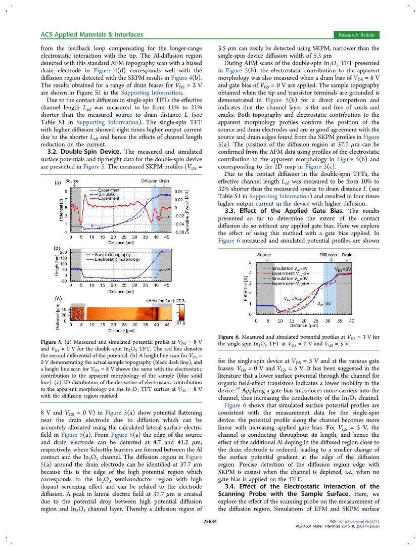
surface potentials and tip height data for the double-spin deviceare presented in Figure 5. The measured SKPM profiles (VDS =
8 V and VGS = 0 V) in Figure 5(a) show potential flatteningnear the drain electrode due to diffusion which can beaccurately allocated using the calculated lateral surface electricfield in Figure 5(a). From Figure 5(a) the edge of the sourceand drain electrode can be detected at 4.7 and 41.2 μm,respectively, where Schottky barriers are formed between the Alcontact and the In2O3 channel. The diffusion region in Figure5(a) around the drain electrode can be identified at 37.7 μmbecause this is the edge of the high potential region whichcorresponds to the In2O3 semiconductor region with highdopant screening effect and can be related to the electrodediffusion. A peak in lateral electric field at 37.7 μm is createddue to the potential drop between high potential diffusionregion and In2O3 channel layer. Thereby a diffusion region of
3.5 μm can easily be detected using SKPM, narrower than thesingle-spin device diffusion width of 5.3 μmDuring AFM scans of the double-spin In2O3 TFT presented
in Figure 5(b), the electrostatic contribution to the apparentmorphology was also measured when a drain bias of VDS = 8 Vand gate bias of VGS = 0 V are applied. The sample topographyobtained when the tip and transistor terminals are grounded isdemonstrated in Figure 5(b) for a direct comparison andindicates that the channel layer is flat and free of voids andcracks. Both topography and electrostatic contribution to theapparent morphology profiles confirm the position of thesource and drain electrodes and are in good agreement with thesource and drain edges found from the SKPM profiles in Figure5(a). The position of the diffusion region at 37.7 μm can beconfirmed from the AFM data using profiles of the electrostaticcontribution to the apparent morphology in Figure 5(b) andcorresponding to the 2D map in Figure 5(c).Due to the contact diffusion in the double-spin TFTs, the
effective channel length Leff was measured to be from 10% to32% shorter than the measured source to drain distance L (seeTable S1 in Supporting Information) and resulted in four timeshigher output current in the device with higher diffusion.
3.3. Effect of the Applied Gate Bias. The resultspresented so far to determine the extent of the contactdiffusion do so without any applied gate bias. Here we explorethe effect of using this method with a gate bias applied. InFigure 6 measured and simulated potential profiles are shown
for the single-spin device at VDS = 3 V and at the various gatebiases: VGS = 0 V and VGS = 5 V. It has been suggested in theliterature that a lower surface potential through the channel fororganic field-effect transistors indicates a lower mobility in thedevice.39 Applying a gate bias introduces more carriers into thechannel, thus increasing the conductivity of the In2O3 channel.Figure 6 shows that simulated surface potential profiles are
consistent with the measurement data for the single-spindevice: the potential profile along the channel becomes morelinear with increasing applied gate bias. For VGS = 5 V, thechannel is conducting throughout its length, and hence theeffect of the additional Al doping in the diffused region close tothe drain electrode is reduced, leading to a smaller change ofthe surface potential gradient at the edge of the diffusionregion. Precise detection of the diffusion region edge withSKPM is easiest when the channel is depleted, i.e., when nogate bias is applied on the TFT.
3.4. Effect of the Electrostatic Interaction of theScanning Probe with the Sample Surface. Here, weexplore the effect of the scanning probe on the measurement ofthe diffusion region. Simulations of EFM and SKPM surface
Figure 5. (a) Measured and simulated potential profile at VDS = 8 Vand VGS = 0 V for the double-spin In2O3 TFT. The red line denotesthe second differential of the potential. (b) A height line scan for VDS =0 V demonstrating the actual sample topography (black dash line), anda height line scan for VDS = 8 V shows the same with the electrostaticcontribution to the apparent morphology of the sample (blue solidline). (c) 2D distribution of the derivative of electrostatic contributionto the apparent morphology on the In2O3 TFT surface at VDS = 8 Vwith the diffusion region marked.
Figure 6. Measured and simulated potential profiles at VDS = 3 V forthe single-spin In2O3 TFT at VGS = 0 V and VGS = 5 V.
ACS Applied Materials & Interfaces Research Article
DOI: 10.1021/acsami.6b10332ACS Appl. Mater. Interfaces 2016, 8, 25631−25636
25634

potential profiles with a full tip and cantilever structure havebeen demonstrated in the literature, where the tip-inducedband bending was considered to be negligible.6,40 Wheninvestigating semiconductor surfaces, the electrostatic forcebetween the tip and sample is nullified by setting the contactpotential difference (VCPD) to be VCPD = VDC, and the tip-induced band bending at the sample surface is considered to bezero.40 This approach to nullify the electrostatic force betweenthe tip and the sample was shown to be valid for metal−metalinfinite plates. However, this nulling is not always valid for ametal−semiconductor material system because the chargedistribution within the semiconductor and within the n-typesilicon tip will depend on the tip−sample separation.4,41
In this work a large change in the potential profiles for thehigher drain biases (VDS > 3 V) was observed due to theelectrostatic interaction of the tip apex with the sample surface(Figure 7). The potential drops between the drain electrode,
diffusion region, and channel layer are additionally increaseddue to the presence of the scanning tip apex. However, whenthe tip bias is adjusted in the simulation to match the surfacepotential directly beneath the tip, as happens in experimentalSKPM measurements, the effect of the tip interaction on thepotential profile is minimal. More detail on the simulatedprobe−sample system is available in the Supporting Informa-tion.
4. CONCLUSIONDifferential potential profile maps measured using SKPM andapparent morphology scans using AFM were used to measurecontact diffusion into the channel of In2O3 TFTs. We show thatusing conventional AFM or SKPM on an unbiased sample willnot reveal this structure adequately. We show that a drain biasmust be applied for the diffusion region to be clearly detectedas a sharp change in the potential profile gradient at theboundary between the depleted channel and the unintention-ally doped region where contact diffusion occurs. Increasing thegate bias reduces the sensitivity of the method due to theaccumulated charge along the length of the channel.Simulations of the electrostatic probe interaction indicate thatthe biased tip does not have a significant effect. We match all ofour findings to simulations with very good agreement.The methodology is applied to detect Al contact diffusion in
In2O3 thin-film transistors, revealing a diffusion region as smallas 3.5 μm, with the effective channel length decreasing by up to
32%. Al diffusion is also found to act as an additional n-typedopant, with an increase in the n-type doping concentration ofthe In2O3 layer from 2 × 10¹⁸ to 8 × 1018 cm−3.This approach can be applied generally to all semi-
conductor−semiconductor or semiconductor−metal interfaces,where interface diffusion is thought to be present but is belowthe detection threshold of standard AFM or SKPM.
■ ASSOCIATED CONTENT*S Supporting InformationThe Supporting Information is available free of charge on theACS Publications website at DOI: 10.1021/acsami.6b10332.
Height line scans for VDS from 0 to 3 V. The values of thedrain current IDS, channel length L, effective channellength Leff, and diffusion region Ldiff at VGS = 10 V andVDS = 16 V for the double-spin and single-spin In2O3TFTs. Simulated tip movement and tip structure used inthe simulation (PDF)
■ AUTHOR INFORMATIONCorresponding Author*E-mail: [email protected] authors declare no competing financial interest.
■ ACKNOWLEDGMENTSIA thanks the Iraqi Cultural Attache for sponsorship andSalahaddin University for ongoing support. YHL and TDA aregrateful to European Research Council (ERC) AMPRO projectno. 280221 for financial support. OK would like to thank theZienkiewicz Scholarship (Swansea University, UK) for financialsupport. The work was partially supported by EPSRC grantEP/K03099X/1.
■ REFERENCES(1) Melitz, W.; Shen, J.; Kummel, A. C.; Lee, S. Kelvin Probe ForceMicroscopy and Its Application. Surf. Sci. Rep. 2011, 66 (1), 1−27.(2) Saive, R.; Scherer, M.; Mueller, C.; Daume, D.; Schinke, J.;Kroeger, M.; Kowalsky, W. Imaging the Electric Potential withinOrganic Solar Cells. Adv. Funct. Mater. 2013, 23 (47), 5854−5860.(3) Tello, M.; Chiesa, M.; Duffy, C. M.; Sirringhaus, H. ChargeTrapping in Intergrain Regions of Pentacene Thin Film Transistors.Adv. Funct. Mater. 2008, 18 (24), 3907−3913.(4) Charrier, D. S. H.; Kemerink, M.; Smalbrugge, B. E.; de Vries, T.;Janssen, R. A. J. Real versus Measured Surface Potentials in ScanningKelvin Probe Microscopy. ACS Nano 2008, 2 (4), 622−626.(5) Muller, K.; Goryachko, A.; Burkov, Y.; Schwiertz, C.; Ratzke, M.;Koble, J.; Reif, J.; Schmeißer, D. Scanning Kelvin Probe andPhotoemission Electron Microscopy of Organic Source-DrainStructures. Synth. Met. 2004, 146 (3), 377−382.(6) Liscio, A.; Palermo, V.; Mullen, K.; Samorì, P. Tip−SampleInteractions in Kelvin Probe Force Microscopy: QuantitativeMeasurement of the Local Surface Potential. J. Phys. Chem. C 2008,112 (44), 17368−17377.(7) Sacha, G. M.; Verdaguer, a.; Martínez, J.; Saenz, J. J.; Ogletree, D.F.; Salmeron, M. Effective Tip Radius in Electrostatic ForceMicroscopy. Appl. Phys. Lett. 2005, 86 (12), 123101.(8) Valdre, G.; Moro, D. 3D Finite Element Analysis of ElectrostaticDeflection of Commercial and FIB-Modified Cantilevers for Electricand Kelvin Force Microscopy: I. Triangular Shaped Cantilevers withSymmetric Pyramidal Tips. Nanotechnology 2008, 19 (40), 405501.(9) Kryvchenkova, O.; Cobley, R. J.; Kalna, K. Self-ConsistentModelling of Tunnelling Spectroscopy on III−V Semiconductors.Appl. Surf. Sci. 2014, 295, 173−179.
Figure 7. Simulation with 0 V bias on the tip (dashed line) and withthe tip bias matched to the measured potential under the tip (opendiamonds) at VDS = 3 V. The potential profile with no tip present isalso shown for comparison (blue line). The tip apex structure with an80 nm radius and a 20 nm tip−sample separation are used.
ACS Applied Materials & Interfaces Research Article
DOI: 10.1021/acsami.6b10332ACS Appl. Mater. Interfaces 2016, 8, 25631−25636
25635

(10) Barnett, C. J.; Kryvchenkova, O.; Wilson, L. S. J.; Maffeis, T. G.G.; Kalna, K.; Cobley, R. J. The Role of Probe Oxide in Local SurfaceConductivity Measurements. J. Appl. Phys. 2015, 117 (17), 174306.(11) Lang, O.; Pettenkofer, C.; Sanchez-Royo, J. F.; Segura, A.; Klein,A.; Jaegermann, W. Thin Film Growth and Band Lineup of In[sub2]O[sub 3] on the Layered Semiconductor InSe. J. Appl. Phys. 1999,86 (10), 5687.(12) King, P.; Veal, T.; Fuchs, F.; Wang, C.; Payne, D.; Bourlange, A.;Zhang, H.; Bell, G.; Cimalla, V.; Ambacher, O.; Egdell, R.; Bechstedt,F.; McConville, C. Band Gap, Electronic Structure, and SurfaceElectron Accumulation of Cubic and Rhombohedral In2O3. Phys. Rev.B: Condens. Matter Mater. Phys. 2009, 79 (20), 205211.(13) Park, J. H.; Yoo, Y. B.; Lee, K. H.; Jang, W. S.; Oh, J. Y.; Chae, S.S.; Lee, H. W.; Han, S. W.; Baik, H. K. Boron-Doped Peroxo-Zirconium Oxide Dielectric for High-Performance, Low-Temperature,Solution-Processed Indium Oxide Thin-Film Transistor. ACS Appl.Mater. Interfaces 2013, 5 (16), 8067−8075.(14) Street, R. A. Thin-Film Transistors. Adv. Mater. 2009, 21 (20),2007−2022.(15) Jiao, Y.; Zhang, X.; Zhai, J.; Yu, X.; Ding, L.; Zhang, W. Bottom-Gate Amorphous In2O3 Thin Film Transistors Fabricated byMagnetron Sputtering. Electron. Mater. Lett. 2013, 9 (3), 279−282.(16) Henning, A. K.; Hochwitz, T.; Slinkman, J.; Never, J.;Hoffmann, S.; Kaszuba, P.; Daghlian, C. Two-Dimensional SurfaceDopant Profiling in Silicon Using Scanning Kelvin Probe Microscopy.J. Appl. Phys. 1995, 77 (5), 1888.(17) Shin, H.; Kim, C.; Lee, B.; Kim, J.; Park, H.; Min, D.-K.; Jung, J.;Hong, S.; Kim, S. Formation and Process Optimization of ScanningResistive Probe. J. Vac. Sci. Technol. B Microelectron. Nanom. Struct.2006, 24 (5), 2417.(18) Koren, E.; Berkovitch, N.; Rosenwaks, Y. Measurement ofActive Dopant Distribution and Diffusion in Individual SiliconNanowires. Nano Lett. 2010, 10 (4), 1163−1167.(19) Sato, Y.; Otake, F.; Hatori, H. A Dependence of Crystallinity ofIn2O3 Thin Films by a Two-Step Heat Treatment of Indium Films onthe Heating Atmosphere. J. Mod. Phys. 2010, 01 (06), 360−363.(20) Robertson, J.; Falabretti, B. Handbook of TransparentConductors; Ginley, D. S., Ed.; Springer US: Boston, MA, 2011.(21) Liu, A.; Liu, G. X.; Zhu, H. H.; Xu, F.; Fortunato, E.; Martins,R.; Shan, F. K. Fully Solution-Processed Low-Voltage Aqueous In2O3Thin-Film Transistors Using an Ultrathin ZrOx Dielectric. ACS Appl.Mater. Interfaces 2014, 6 (20), 17364−17369.(22) Lin, Y.-H.; Faber, H.; Labram, J. G.; Stratakis, E.; Sygellou, L.;Kymakis, E.; Hastas, N. A.; Li, R.; Zhao, K.; Amassian, A.; Treat, N. D.;McLachlan, M.; Anthopoulos, T. D. High Electron Mobility Thin-FilmTransistors Based on Solution-Processed Semiconducting Metal OxideHeterojunctions and Quasi-Superlattices. Adv. Sci. 2015, 2 (7),1500058.(23) Faber, H.; Lin, Y.-H.; Thomas, S. R.; Zhao, K.; Pliatsikas, N.;McLachlan, M. A.; Amassian, A.; Patsalas, P. A.; Anthopoulos, T. D.Indium Oxide Thin-Film Transistors Processed at Low Temperaturevia Ultrasonic Spray Pyrolysis. ACS Appl. Mater. Interfaces 2015, 7 (1),782−790.(24) Kumm, J.; Chacko, R. V.; Samadi, H.; Hartmann, P.; Eberlein,D.; Jager, U.; Wolf, A. Long-Term and Annealing Stable, SolderablePVD Metallization with Optimized Al Diffusion Barrier. EnergyProcedia 2015, 77, 374.(25) Kolawa, E.; Garland, C.; Tran, L.; Nieh, C. W.; Molarius, J. M.;Flick, W.; Nicolet, M.-A.; Wei, J. Indium Oxide Diffusion Barriers forAl/Si Metallizations. Appl. Phys. Lett. 1988, 53 (26), 2644.(26) Armigliato, A.; Valdre, G. Analytical Electron Microscopy of Al/TiN Contacts on Silicon for Applications to Very Large ScaleIntegrated Devices. J. Appl. Phys. 1987, 61 (1), 390.(27) Atlas User’s Manual; 2007.(28) Girtan, M.; Rusu, G. On the Size Effect in In2O3 Thin Films.Mater. Sci. Eng., B 1999, 166−172.(29) Zhuang, J.; Lo, W.-S.; Zhou, L.; Sun, Q.-J.; Chan, C.-F.; Zhou,Y.; Han, S.-T.; Yan, Y.; Wong, W.-T.; Wong, K.-L.; Roy, V. a. L. Photo-
Reactive Charge Trapping Memory Based on Lanthanide Complex.Sci. Rep. 2015, 5, 14998.(30) Huang, T.-S.; Su, Y.-K.; Wang, P.-C. Study of Organic Thin FilmTransistor with Polymethylmethacrylate as a Dielectric Layer. Appl.Phys. Lett. 2007, 91 (9), 092116.(31) Schonherr, H.; Vancso, G. J. Scanning Force Microscopy ofPolymers; Springer Berlin Heidelberg: Berlin, Heidelberg, 2010.(32) Riedel, C.; Schwartz, G. a; Arinero, R.; Tordjeman, P.; Leveque,G.; Alegría, a; Colmenero, J. Nanoscale Dielectric Properties ofInsulating Thin Films: From Single Point Measurements toQuantitative Images. Ultramicroscopy 2010, 110 (6), 634−638.(33) Bayerl, D. J.; Wang, X. Three-Dimensional Kelvin ProbeMicroscopy for Characterizing In-Plane Piezoelectric Potential ofLaterally Deflected ZnO Micro-/Nanowires. Adv. Funct. Mater. 2012,22 (3), 652−660.(34) Horcas, I.; Fernandez, R.; Gomez-Rodríguez, J. M.; Colchero, J.;Gomez-Herrero, J.; Baro, A. M. WSXM: A Software for ScanningProbe Microscopy and a Tool for Nanotechnology. Rev. Sci. Instrum.2007, 78 (1), 013705.(35) Lord, A. M.; Maffeis, T. G.; Kryvchenkova, O.; Cobley, R. J.;Kalna, K.; Kepaptsoglou, D. M.; Ramasse, Q. M.; Walton, A. S.; Ward,M. B.; Koble, J.; Wilks, S. P. Controlling the Electrical TransportProperties of Nanocontacts to Nanowires. Nano Lett. 2015, 15 (7),4248−4254.(36) Hamberg, I.; Granqvist, C. G. Evaporated Sn-Doped In2O3Films: Basic Optical Properties and Applications to Energy-EfficientWindows. J. Appl. Phys. 1986, 60 (11), R123.(37) Li, C.; Minne, S.; Hu, Y.; Ji, M.; He, J.; Mittel, H.; Kelly, V.;Erina, N.; Guo, S.; Mueller, T. Peak Force Kelvin Probe ForceMicroscopy. Bruker Appl. Note # 2013, 140, 1−14.(38) Sacha, G. M.; Saenz, J. J. Cantilever Effects on ElectrostaticForce Gradient Microscopy. Appl. Phys. Lett. 2004, 85 (13), 2610.(39) Luttich, F.; Lehmann, D.; Friedrich, M.; Chen, Z.; Facchetti, A.;von Borczyskowski, C.; Zahn, D. R. T.; Graaf, H. Interface Propertiesof OFETs Based on an Air-Stable N-Channel Perylene TetracarboxylicDiimide Semiconductor. Phys. Status Solidi A 2012, 209 (3), 585−593.(40) Zerweck, U.; Loppacher, C.; Otto, T.; Grafstrom, S.; Eng, L.Accuracy and Resolution Limits of Kelvin Probe Force Microscopy.Phys. Rev. B: Condens. Matter Mater. Phys. 2005, 71 (12), 125424.(41) Hudlet, S.; Saint Jean, M.; Roulet, B.; Berger, J.; Guthmann, C.Electrostatic Forces between Metallic Tip and SemiconductorSurfaces. J. Appl. Phys. 1995, 77 (7), 3308.
ACS Applied Materials & Interfaces Research Article
DOI: 10.1021/acsami.6b10332ACS Appl. Mater. Interfaces 2016, 8, 25631−25636
25636


![Cronfa - Swansea University Open Access Repository · 2017-05-03 · terms of the repository licence. ... (that was previously calibrated against Silvaco's [23] NEGF simulations [24])](https://img.dokumen.tips/doc/110x75/5b2a89197f8b9a1a298b4751/cronfa-swansea-university-open-access-repository-2017-05-03-terms-of-the.jpg)


![Cronfa - Swansea University Open Access Repository · ô ½ ·W=m] Y](https://img.dokumen.tips/doc/110x75/5e086d1104eac94d302c30f1/cronfa-swansea-university-open-access-repository-wm-y.jpg)

