Embed Size (px)
Citation preview

www.ti.com
FEATURES
APPLICATIONS
DESCRIPTION
C2P
VIN
EN S
WSW S
UP
D1L1
10uHVin2.5V to6.0V
C9
68 pF
R239k W
R1
470k W
FB
Vs
15V/1.0A
C522 mF
C622 mF
C722 mF
C1
22 mF
C222 mF
C3
22 mF C4
1 mF
COMP
C2N
HVS
CTRL
DRN
POS1
NEG1
OUT1
POS2
NEG2
OUT2
ADLY
GDLY
SS P
OS3
BGND
OUT3
AGND
REF
FBN
RHVS
FBP
POUT
C1P
C1N
PGND
PGND
VGH
DRVN
1
23
D2
D3
R7
160k W
R8
39k W
C20
220nF
C16330nF
VGL
-5V/50mA
C15
330nF
VGH
27.5V/50mA
R5300kW
R6
16k W
High Voltage
SwitchControl
BoostConverter
D
S
Positive Charge
Pumpx2or x3
SUP
C14
100pF
C13
1 mF
C12
330nF
R4
220k W
R3
30 k W
C101 nF
C11
330nF
C8
1 mF
C17
22nF
C18
22nF
C19
22nF
R10
1k W
TPS65165SLVS723A–DECEMBER 2006–REVISED MAY 2007
Compact LCD Bias IC With High Speed Amplifiers for TV and Monitor TFT-LCD Panels
Amplifiers• 2.5 V to 6.0 V Input Voltage Range – 50 MHz 3 db Bandwidth• Vs Output Voltage up to 18 V – Slew Rate 45 V/µs
– 1%-Accurate Boost Converter With 4.5 A – 215 mA Short Circuit CurrentSwitch Current • High Voltage Test Mode (HVS)
– 600 kHz Fixed Frequency PWM Operation • Thermal Shutdown– Overvoltage Protection • 40-Pin 5×5-mm QFN Package– Adjustable Softstart
• Regulated Positive Charge Pump Converter• LCD MonitorVGH• LCD TV Panel• Integrated Gate Voltage Shaping of VGH
• Regulated Negative Charge-Pump Driver VGL• Adjustable Sequencing for Vs and VGH• 3 Integrated High-Speed Operational
The TPS65165 is a Compact LCD Bias IC with 3 high-speed operational amplifiers for gamma correction and/orVCOM supply. The device generates all 3 voltage rails for TFT-LCD displays (Vs, VGL and VGH). The deviceincorporates a high-voltage switch that can be controlled by a logic signal from the timing controller (TCON) toprovide the gate-voltage modulation for VGH. If this function is not required, the CTRL pin can be tied high.
Please be aware that an important notice concerning availability, standard warranty, and use in critical applications of TexasInstruments semiconductor products and disclaimers thereto appears at the end of this data sheet.
PRODUCTION DATA information is current as of publication date. Copyright © 2006–2007, Texas Instruments IncorporatedProducts conform to specifications per the terms of the TexasInstruments standard warranty. Production processing does notnecessarily include testing of all parameters.www.BDTIC.com/TI

www.ti.com
ABSOLUTE MAXIMUM RATINGS
DISSIPATION RATINGS (1)
RECOMMENDED OPERATING CONDITIONS
TPS65165SLVS723A–DECEMBER 2006–REVISED MAY 2007
The device also features a high-voltage stress test, where the output voltage of VGH is typically set to 30 V, andthe output voltage of Vs is programmable to any higher voltage. The high-voltage stress test is enabled bypulling the HVS pin high. Adjustable sequencing is implemented, and can be programmed by selecting thecapacitor values connected to ADLY and GDLY. The device consists of a boost converter to provide the sourcevoltage Vs operating at a fixed switching frequency of 600 kHz. A fully integrated positive charge pump,switching automatically between doubler and tripler mode provides an adjustable regulated TFT gate on voltageVGH. A negative charge pump driver provides adjustable regulated output voltage VGL. To minimize externalcomponents the charge pumps for VGH and VGL operate at a fixed switching frequency of 1.2 MHz. The deviceincludes safety features like overvoltage protection of the boost converter, short circuit protection of VGH andVGL as well as thermal shutdown.
ORDERING INFORMATION (1)
TA ORDERING QFN PACKAGE PACKAGE MARKING
–40°C to 85°C TPS65165RSBR RSB TPS65165
(1) The TPS65165RSBR is available taped and reeled and shipped in quantities of 3000 devices per reel.
over operating free-air temperature range (unless otherwise noted) (1)
VALUE UNIT
Input voltage range VIN(2) –0.3 V to 7.0 V
Voltage range at EN, CTRL, HVS –0.3 V to 7.0 V
SUP 22
Voltage on SW 25 V
POUT, VGH, DRN 32
Peak switch current Internally limited V
HBM 2 kV
ESD rating MM 200 V
CDM 750 V
Continuous total power dissipation See Dissipation Rating Table
TJ Operating junction temperature range –40 to 150 °C
TA Operating ambient temperature range –40 to 85 °C
Tstg Storage temperature range –65 to 150 °C
(1) Stresses beyond those listed under absolute maximum ratings may cause permanent damage to the device. These are stress ratingsonly, and functional operation of the device at these or any other conditions beyond those indicated under recommended operatingconditions is not implied. Exposure to absolute–maximum–rated conditions for extended periods may affect device reliability.
(2) All voltage values are with respect to network ground terminal.
PACKAGE RθJA TA < 25°C TA = 70°C TA = 85°CPOWER RATING POWER RATING POWER RATING
40-pin QFN 30°C/W 3.3 W 1.8 W 1.3 W
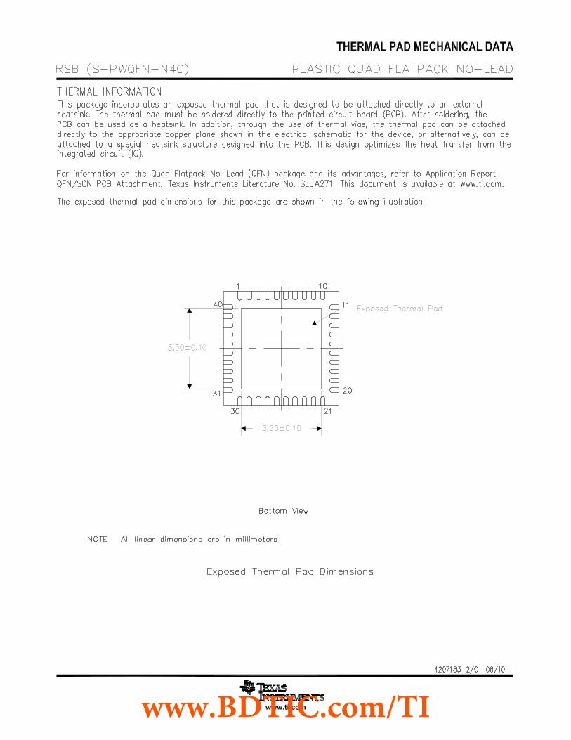
(1) Exposed thermal die is soldered to the PCB using thermal vias. Refer to Texas Instruments Application report (SLUA271) QFN/SONPCB Attachment.
MIN NOM MAX UNIT
VIN Input voltage range 2.5 6.0 V
TA Operation ambient temperature –40 85 °C
TJ Operating junction temperature –40 125 °C
2 Submit Documentation Feedbackwww.BDTIC.com/TI

www.ti.com
ELECTRICAL CHARACTERISTICS
TPS65165SLVS723A–DECEMBER 2006–REVISED MAY 2007
VIN=5.0V, Vs=15V, HVS=low, EN=CTRL=high, TA = –40°C to 85°C, typical values are at TA = 25°C (unless otherwise noted)
PARAMETER TEST CONDITIONS MIN TYP MAX UNIT
SUPPLY CURRENT
VIN Input voltage range 2.5 6.0 V
IQVIN No load quiescent current into VIN Device not switching 1 1.5 mA
IQSUP No load quiescent current into SUP Device not switching 20 25 mA
Shutdown current into VIN Vin=6V 1ISD µA
Shutdown current into SUP Vin=6V, SUP = Vin-0.5V 8
Vin rising 2.3 2.5 VVUVLO Under-voltage lockout threshold
Vin falling 2.2 2.3 V
Thermal shutdown Temperature rising 155 °C
Thermal shutdown hysteresis 5 °C
LOGIC SIGNALS EN, CTRL, HVS
Vth Threshold voltage Vin = 2.5 V to 6.0 V 0.4 1.4 V
II Input leakage current ±0.01 ±0.1 µA
HIGH VOLTAGE STRESS TEST (HVS)
VPOUT Positive charge pump output voltage HVS = high 28.5 30 31.5 V
RHVS RHVS pull down resistance HVS = high, Vin = 2.5 V to 6.0 V, 0.5 1 1.5 kΩIHVS = 100 µA
IRHVS RHVS leackage current HVS = low, VRHVS = 1.5 V 100 nA
MAIN BOOST CONVERTER Vs
Vs Output voltage range 7 18 V
VFB Feedback regulation voltage 1.136 1.146 1.154 V
IFB Feedback input bias current VFB = 1.146 100 nA
Vs = 15 V, ISW = 500 mA, 75 140N-MOSFET on-resistance (Q1) mΩVs = 7 V, ISW = 500 mARDS(ON)
Vs = 15 V; ISW = 100 mA, 10 16P-MOSFET on-resistance (Q2) ΩVs = 7 V; ISW = 100 mA
IMAX Maximum P-MOSFET peak switch current 1 A(Q2)
ILIM N-MOSFET switch current limit (Q1) 4.4 5.5 6.6 A
Ileak Switch leakage current VSW = 15 V 10 µA
Vovp Output overvoltage protection FB = GND, Vout rising 19.5 20 21 V
fOSC Oscilator frequency 480 600 720 kHz
Line regulation Vin=3.0V to 6.0V, Iout=100mA 0.045 %/V
Load regulation Iout=100mA to 700mA, Vin=5.0V 0.23 %/A
NEGATIVE CHARGE PUMP VGL
VGL Output voltage range –2 V
VFB Feedback regulation voltage –48 0 48 mV
IFB Feedback input bias current VFB = 0 V 100 nA
Vref Reference voltage VIN = 2.5 V to 6 V, IREF = 10µ A 1.205 1.213 1.219 V
RDSon Q7 P-Channel switch RDSon IDRVN = 40 mA 4.4 Ω
IDRN = 40 mA, VFBN = VFBNnominal– 5% 130 300 mVVDropN Current sink voltage drop (1)
IDRN = 100 mA, VFBN = VFBNnominal– 5% 280 450 mV
POSITIVE CHARGE PUMP (POUT)
VPOUT Output voltage range 30 V
VFB Feedback regulation voltage CTRL = GND, VGH = open 1.187 1.214 1.238 V
IFB Feedback input bias current FBO = 1.214 V 100 nA
(1) The maximum charge pump output current is half the drive current IDRNof the internal current source or sink
3Submit Documentation Feedbackwww.BDTIC.com/TI

www.ti.comTPS65165SLVS723A–DECEMBER 2006–REVISED MAY 2007
ELECTRICAL CHARACTERISTICS (continued)VIN=5.0V, Vs=15V, HVS=low, EN=CTRL=high, TA = –40°C to 85°C, typical values are at TA = 25°C (unless otherwise noted)
PARAMETER TEST CONDITIONS MIN TYP MAX UNIT
Vd D1–D4 Schottky diode forward voltage ID1-D4 = 40 mA 610 800 mV
Doubler Mode (x2); IPOUT = 20 mA 94 Ω
Doubler Mode (x2); IPOUT = 50 mA 63 ΩReff Effective output resistance
Tripler Mode (x3); IPOUT = 20 mA 141 Ω
Tripler Mode (x3); IPOUT = 50 mA 94 Ω
HIGH VOLTAGE SWITCH VGH
POUT to VGH RDSon CTRL = high, POUT = 27 V, I = 20 mA 8.5 16 ΩRDSon
DRN to VGH RDSon CTRL = low, VDRN = 5 V, I = 20 mA 38 62 Ω
IDRN DRN input current CTRL = low, VVGH = VDRN 10 µA
tdly CTRL to VGH propagation delay CTRL = high to low, POUT = 27 V, 125 nsVDRN = GND
RVGH VGH pull down resistance EN = low, I = 20 mA 1 kΩ
CONTROL AND SOFTSTART ADLY, GDLY, SS
IADLY Drive current into delay capacitor ADLY VADLY = 1.213 V 3.5 4.8 6.2 µA
IGDLY Drive current into delay capacitor GDLY VADLY = 1.213 V 3.5 4.8 6.2 µA
ISS SS charge current VSS = 0 V 2.8 4.5 6.2 µA
OPERATIONAL AMPLIFIERS 1, 2, 3
Vos Input offset voltage VCM = Vs/2 –15 3 18 mV
IB Input bias current VCM = Vs/2 0 3 µA
VCM Common mode input voltage range 0 Vs V
CMRR Common mode rejection ratio VCM = 7.5 V 55 75 dB
AVOL Open loop gain 0.5 V ≤ Vout ≤ 14.5 V, No load 50 dB
VOL Output voltage swing low IOUT = 10 mA 100 200 mV
VOH Output voltage swing high IOUT = 10 mA 100 Vs–200 mV
Isc Short circuit current 120 215 mA
IO Output current VOUT = 7.5V , Input offset voltage 10 mV 90 170 mA
PSRR Power supply rejection ratio 80 dB
SR Slew rate AV = 1, VIN = 2 Vpp 45 V/µs
BW – 3dB Bandwidth AV = 1, VOUT = 50 mVpp, Output High 50 MHzImpedance
GBWP Gain bandwidth product 26 MHz
Roff Pull down resistor 10 kΩ
4 Submit Documentation Feedbackwww.BDTIC.com/TI

www.ti.com
PIN ASSIGNMENT
6
7
8
9
10
25
24
23
22
21111213141516
353637383940
ExposedThermal Die*
181920
30
29
28
27
26
1
2
3
4
5
313233
17
34
C1N
C1P
POUT
FBP
DRN
VGH
FB
COMP
RHVS
NC
POS3
OUT3
NC A
DLY
GDL
Y
CTRL
HVS
DRVN
NC
SS
C2N
C2P
BGND
SUP
POS1
NEG1
OUT1
OUT2
NEG2
POS2
SW
SW
PGND
PGND
NC
EN
REF
AGND
VIN
FBN
TPS65165SLVS723A–DECEMBER 2006–REVISED MAY 2007
NOTE: The exposed thermal die is connected to AGNG. NC pin is internally not connected.
TERMINAL FUNCTIONS
TERMINALI/O DESCRIPTION
NAME NO.
Negative terminal of the flying capacitor for the positive charge pump. Typically a 330nF flying capacitor isC2N 1 I/O required.
Positive terminal of the flying capacitor for the positive charge pump. Typically a 330nF flying capacitor isC2P 2 I/O required.
BGND 3 Low noise ground for the operational amplifier.
Supply input for the operational amplifier and charge pump stages. Connect to the main output Vs, with aSUP 4 I 1-µF bypass capacitor.
POS1 5 I Non-inverting input of Operational Amplifier 1.
NEG1 6 I Inverting input of the Operational Amplifier 1.
Output of Operational Amplifier 1. When the device is disabled, the output is pulled to GND via a 1-kΩOUT1 7 O resistor.
Output of Operational Amplifier 2. When the device is disabled, the output is pulled to GND via a 1-kΩOUT2 8 O resistor.
NEG2 9 I Inverting input of Operational Amplifier 2.
POS2 10 I Non-inverting input of Operational Amplifier 2.
POS3 11 I Non-inverting input of Operational Amplifier 3.
Output of Operational Amplifier 3. When the device is disabled, the output is pulled to GND via a 1-kΩOUT3 12 O resistor.
13, 19,NC Not connected. These pin can be connected to GND to improve the thermal resistance of the package.26, 31
Adjustable EN high-to-start-up delay of the main boost converter, negative and positive charge pump.ADLY 14 O Connect a capacitor from this pin to GND to set the desired delay time. (See SETTING THE DELAY TIMES
ADLY, GDLY)
Adjustable EN high-to-enable delay of the high-voltage switch Q8 (gate voltage shaping). Connect aGDLY 15 O capacitor from this pin to GND to set the desired delay time. (See SETTING THE DELAY TIMES ADLY,
GDLY)
CTRL 16 I Logic control input for the internal high voltage switch (gate voltage shaping).
5Submit Documentation Feedbackwww.BDTIC.com/TI

www.ti.comTPS65165SLVS723A–DECEMBER 2006–REVISED MAY 2007
PIN ASSIGNMENT (continued)
TERMINAL FUNCTIONS (continued)
TERMINALI/O DESCRIPTION
NAME NO.
Logic control input to enable High Voltage Stress Test. With HVS=low the high voltage stress test is disabled.HVS 17 I With HVS=high the high voltage stress test is enabled.
Drive pin for the negative charge pump converter generating VGL. Using a single stage charge pump invertsDRVN 18 I/O the voltage present at the main boost converter Vs and regulates it down to the desired voltage programmed
by the feedback divider.
SS 20 O Softstart for the main boost converter generating Vs. Connect a capacitor to this pin to set the softstart time.
FBN 21 I Feedback of the negative charge pump converter.
Reference output. Connect a 220-nF capacitor directly from REF pin to AGND to minimize possible noiseREF 22 O coupling into the reference of the IC.
AGND 23 I Analog Ground , positive and negative charge pump ground.
VIN 24 I Supply pin for the IC. Bypass this pin with a 1-µF capacitor directly to GND.
EN 25 I Enable pin of the IC. EN=high enables the IC. EN= low disables the IC. This pin must be terminated.
PGND 27, 28 Power Ground for the boost converter.
SW 29, 30 I/O Switch pin of the boost regulator generating Vs
This resistor sets the voltage of the boost converter Vs when the High Voltage Stress test is enabled.RHVS 32 I (HVS=high). With HVS=high the RHVS pin is pulled to GND which sets the output voltage for the boost
converter. When HVS is disabled (HVS=low) the RHVS pin is high impedance.
COMP 33 O Compensation for the regulation loop of the boost converter generating Vs.
FB 34 I Feedback of the boost converter generating Vs.
VGH 35 O This is the output voltage of the internal high voltage switch, controlled by the CTRL signal.
DRN 36 I/O Connect the discharge resistor for the Gate voltage shaping to this pin.
FBP 37 I This is the feedback for the positive charge pump converter generating VGH
Output of the positive charge pump which is internally connected to the high voltage switch Q2. Connect aPOUT 38 O 1-µF output capacitor to this pin as well as the feedback divider to set the output voltage for the positive
charge pump respectively for VGH.
Positive terminal of the flying capacitor for the positive charge pump. Typically a 330-nF flying capacitor isC1P 39 I/O required.
Negative terminal of the flying capacitor for the positive charge pump. Typically a 330-nF flying capacitor isC1N 40 I/O required.
6 Submit Documentation Feedbackwww.BDTIC.com/TI

www.ti.com
C2P
VIN EN
SW
SW
SU
P
D1L1
10uHVin2.5V to 6.0V
C9
68 pF
R239 kW
R1
470 kW
FB
Vs
15V/1.0A
C522 mF
C622 mF
C722mF
C1
22mF
C222 mF
C3
22 mF C4
1 mF
COMP
C2N
HVS
CTRL
DRN
POS1
NEG1
OUT1
POS2
NEG2
OUT2
AD
LY
GD
LY
SS
PO
S3
BG
ND
OU
T3
AG
ND
REF
FBN
RHVS
FBP
POUT
C1P
C1N
PGND
PGND
VGH
DRVN
1
23
D2
D3
R7
160 kW
R8
39 kW
C20
220nF
C16330 nF
VGL
-5V/50mA
C15
330 nF
VGH
27.5V/50mA
R5300kW
R6
16 kW
High Voltage
Switch Control
Boost Converter
D
S
Positive Charge
Pumpx2 or x3
SU
P
C14
100 pF
C13
1 mF
C12
330nF
R4
220 kW
R3
30 kW
C101 nF
C11
330 nF
C8
1 mF
C17
22 nF
C18
22 nF
C19
22 nF
R10
1kW
TPS65165SLVS723A–DECEMBER 2006–REVISED MAY 2007
BLOCK DIAGRAM
7Submit Documentation Feedbackwww.BDTIC.com/TI

www.ti.com
TYPICAL CHARACTERISTICS
TABLE OF GRAPHS
V
10 V/ div
SW
I
1A/ div
L
V
50 mV/ div
O
400 ns / div
V= 5.0 V
V= 15 V / 700 mAIN
O
40
50
60
70
80
90
100
02004006008001000
IOUT –mA
V= 2.7 V IN
V=15
VGH=VGL=no load, switchingOpAmp operating, no load
S
EFFICIENCY–%
V= 3.3 V IN
V= 5.0 V IN
TPS65165SLVS723A–DECEMBER 2006–REVISED MAY 2007
FIGURE
MAIN BOOST CONVERTER (Vs)
η Efficiency, main boost converter Vs vs Load current Figure 1
PWM operation at nominal load current Figure 2
PWM operation at light load current Figure 3
Load transient response Figure 4
Softstart boost converter VS Figure 5
Overvoltage protection Figure 6
SYSTEM FUCTIONALITY
Power-on sequencing Figure 7
Gate voltage shaping VGH Figure 8
NEGATIVE CHARGE PUMP DRIVER
VGL vs load current Figure 9
POSITIVE CHARGE PUMP
VGH vs load current (doubler mode) Figure 10
VCOM BUFFERS
Input to output offset voltage vs Opamp 1 load current Figure 11
Input to output offset voltage vs Opamp 2 load current Figure 12
Input to output offset voltage vs Opamp 3 load current Figure 13
EFFICIENCY, MAIN BOOST CONVERTERvs
LOAD CURRENT PWM OPERATION NOMINAL LOAD CURRENT
Figure 1. Figure 2.
8 Submit Documentation Feedbackwww.BDTIC.com/TI

www.ti.com
I
100 mA to600 mA
L
V
200 mV/ div
O1
100 s / divm
V = 5.0 V
V = 15 VIN
S
V
10 V/ div
SW
I
1 A/ div
L
V
50 mV/ div
O
400 ns / div
V = 5.0 V
V = 15 V / 50 mAIN
O
V
10 V/ div
S
I
500 mA/ div
L
V
5 V/ div
IN
2.0 ms / div
V = 5.0 V
V = 15 V
I = 100 mA
C = 100 nF
IN
O
OUT
SS
V
10 V/ div
SW
I
2 A/ div
L
V
2 V / div16 V offset
O
40 s / divm
V = 5.0 V
V = 15 V / 100 mAIN
O
V
5 V / divIN
VGL5 V / div
VGH20 V / div
2.0 ms / div
V = 5.0 V
V = 15 V
ADLY = 22 nFGDLY = 47nF
IN
O
V
10 V / divS
CTRL5 V
/ div
VGH10 V/ div
4.0 s / divm
DRN = 1.5 k to V
VGH = 1 nF capacitive load to represent panel
W S
TPS65165SLVS723A–DECEMBER 2006–REVISED MAY 2007
PWM OPERATION AT LIGHT LOAD CURRENT LOAD TRANSIENT RESPONSE
Figure 3. Figure 4.
SOFTSTART BOOST CONVERTER - VS OVERVOLTAGE PROTECTION
Figure 5. Figure 6.
POWER-ON SEQUENCING GATE VOLTAGE SHAPING - VGH
Figure 7. Figure 8.
9Submit Documentation Feedbackwww.BDTIC.com/TI

www.ti.com
I – mAOUT
V = 15 V
VGL = 5 VS
0 10 20 30 40 50 60 70 80 90 100
–5.10
–5.05
–5.00
–4.95
–4.90
–4.85
–4.80
VG
L–
V T = –40°CA
T = 25°C
T = 85°CA
A
I – mAOUT
V = 15 V
VGH = 24 V
C = 2 1 mF / 35 V
S
OUT ´
0 10 20 30 40 50 60 70 80 90 100
24.6
24.4
24.2
24.0
23.8
23.6
23.4
23.2
23.0
22.8
22.6
VG
H–
V
T = –40°CA
T = 25°C
T = 85°CA
A
V – VIN
Unity Gain BufferV = 15 VS
20
15
10
5
0
–5
–10
–15
–20
V–
VO
FF
SE
T
I = –80OUT
I = –50
I = –20
I = –10
I = no load
I = 10
I = 20
I = 50
I = 80
OUT
OUT
OUT
OUT
OUT
OUT
OUT
OUT
0 1 2 3 4 5 6 7 8 9 10 11 12 13 14 15
V – VIN
Unity Gain BufferV = 15 VS
20
15
10
5
0
–5
–10
–15
–20
V–
VO
FF
SE
T
I = –80OUT
I = –50
I = –20
I = –10
I = no load
I = 10
I = 20
I = 50
I = 80
OUT
OUT
OUT
OUT
OUT
OUT
OUT
OUT
0 1 2 3 4 5 6 7 8 9 10 11 12 13 14 15
V – VIN
Unity Gain BufferV = 15 VS
20
15
10
5
0
–5
–10
–15
–20
V–
VO
FF
SE
T
I = –80OUT
I = –50
I = –20
I = –10
I = no load
I = 10
I = 20
I = 50
I = 80
OUT
OUT
OUT
OUT
OUT
OUT
OUT
OUT
0 1 2 3 4 5 6 7 8 9 10 11 12 13 14 15
TPS65165SLVS723A–DECEMBER 2006–REVISED MAY 2007
VGHVGL vs LOAD CURRENT vs LOAD CURRENT - DOUBLER STAGE
Figure 9. Figure 10.
INPUT TO OUTPUT OFFSET VOLTAGE INPUT TO OUTPUT OFFSET VOLTAGEvs OPAMP 1 LOAD CURRENT vs OPAMP 2 LOAD CURRENT
Figure 11. Figure 12.
INPUT TO OUTPUT OFFSET VOLTAGEvs OPAMP 3 LOAD CURRENT
Figure 13.
10 Submit Documentation Feedbackwww.BDTIC.com/TI

www.ti.com
APPLICATION INFORMATION
EN
ADLY
VIN
AGND
UVLO
Undervoltage
lockout
2.3V typ
Thermal
Shutdown latch
155deg °C typ
Vref
1.213V
REF
30uA
Vref
3.5k
Start Boost
converter,negative
and positive charge
pump
Ichg
Voltage
clamp
5.8V max
Regulator2
4.8V typ
Regulator1
Clamps at13.6V
GDLY
Vref
3.5k
Enable Gate voltage
shaping block
Ichg
Voltage
clamp
5.8V max
SUP
Driver supply
Driver Logic
supply
Vin
Vin
THERMAL SHUTDOWN
TPS65165SLVS723A–DECEMBER 2006–REVISED MAY 2007
Figure 14. Control Block TPS65165
The thermal-shutdown feature prevents damage from excessive heat and power dissipation. Typically thethermal-shutdown threshold is 155°C. When the device enters thermal-shutdown then the device does notrestart automatically. The device can only be restarted by cycling the input voltage below itsundervoltage-lockout threshold or by cycling the enable EN to ground.
11Submit Documentation Feedbackwww.BDTIC.com/TI

www.ti.com
UNDERVOLTAGE LOCKOUT
REFERENCE OUTPUT, REF
START-UP SEQUENCING
VGL
ADLY
Fall timedepends outputcapacitor value and load
current
GDLY VGH With CTRL= High
EN
Vs
SETTING THE DELAY TIMES ADLY, GDLY
Cdly 5 A td
Vref
5 A td1.213V (1)
TPS65165SLVS723A–DECEMBER 2006–REVISED MAY 2007
APPLICATION INFORMATION (continued)
To avoid device malfunction at low input voltages, an undervoltage lockout is included which enables the deviceonly when the input voltage exceeds 2.3 V.
The device provides a reference output that is used to regulate the negative charge pump. In order to have astable reference voltage, a 220-nF bypass capacitor is required, connected directly from REF to AGND. Thereference output has a current capability of 30 µA which should not be exceeded. Because of this, the feedbackresistor value from FBN to REF should not be smaller than 40 kΩ.
Start-up sequencing can be controlled by adjusting the delay times ADLY and GDLY. After the delay time set byADLY passed by, the boost converter, negative and positive charge pumps start at the same time. VGH will onlygo high once the delay time, set by GDLY passed by and the signal applied to CTRL is high.
Figure 15. Power-On Sequencing
Connecting an external capacitor to the ADLY and GDLY pin sets the delay time. If no delay time is requiredthese pins can be left open. To set the delay time, the external capacitor connected to ADLY and GDLY ischarged with a constant current source (typically 5 µA). The delay time is terminated when the capacitor voltagehas reached the internal reference voltage of Vref = 1.213 V. The external delay capacitor is calculated by:
with td = Desired delay time
12 Submit Documentation Feedbackwww.BDTIC.com/TI

www.ti.com
BOOST CONVERTER
600kHz
Oszillator
VFB
1.154V
Comparator
GMAmplifier
Sawtooth
Generator
VFB
1.154
VIN SWSW
PGND
PGND
Q1
GMAmplifier
Low Gain
Current limit
and
Soft Start
Q2
SUP
Vref
Vref
Overvoltage
Comparator
OVP
Control Logic
SUP
Softstart
HVS
70Ohm
EN
SS
COMP
FB
RHVS
SOFTSTART BOOST CONVERTER
TPS65165SLVS723A–DECEMBER 2006–REVISED MAY 2007
APPLICATION INFORMATION (continued)
The TPS65165 boost converter block is shown in Figure 16. The boost converter operates with PWM (PulseWidth Modulation) and a fixed switching frequency of 600 kHz. The converter uses a unique fast-response,voltage-mode controller scheme with input voltage feedforward. This achieves excellent line and load regulation(0.2%/A load regulation typical) and allows the use of small external components. To increase the flexibility inthe selection of external component values, the device uses external loop compensation. Although the boostconverter looks like a non-synchronous boost converter topology operating in discontinuous conduction mode, atlight loads, the TPS65165 maintains continuous conduction even at minimal load currents. This is achieved witha novel architecture using an external Schottky diode with an integrated MOSFET in parallel connected betweenSW pin and the SUP pin. The purpose of this MOSFET is to allow the current to go below ground, which is thecase at light load conditions. For this purpose, a small integrated P-Channel MOSFET (Q2) with a typical RDSONof 10 Ω is sufficient. When the inductor current is positive, the external Schottky diode with the lower forwardvoltage carries the current. This causes the converter to operate with a fixed frequency in continuous-conductionmode over the entire load-current range. This avoids ringing on the switch pin as seen with a typicalnon-synchronous boost converter, and allows a simpler compensation network.
Figure 16. Boost Converter Block TPS65165
To minimize inrush current during start-up, an external capacitor connected to the softstart pin (SS) is used toslowly ramp up the internal current limit of the boost converter. The larger the capacitor, the slower the ramp-upof the current limit, and the longer the softstart time. A 22-nF capacitor is usually sufficient for typicalapplications.
13Submit Documentation Feedbackwww.BDTIC.com/TI

www.ti.com
HIGH VOLTAGE STRESS TEST BOOST CONVERTER AND POSITIVE CHARGE PUMP
Vs HVS VFBR1 R2 R4
R2 R4 1.146V
R1 R2 R4R2 R4
R4 R1 R2
Vs HVS
VFB 1 R2 R1
(2)
OVERVOLTAGE PROTECTION BOOST CONVERTER
INPUT CAPACITOR SELECTION VIN, SUP
TPS65165SLVS723A–DECEMBER 2006–REVISED MAY 2007
APPLICATION INFORMATION (continued)
The TPS65165 incorporates a high voltage stress test where the output voltage of the boost converter Vs andthe positive charge pump POUT are set to a higher output voltage compared to the nominal programmed outputvoltage. The High Voltage Stress test is enabled by pulling the HVS pin to high. With HVS=high the voltage onPOUT, respectively VGH is regulated to a fixed output voltage of 30 V. The boost converter Vs is programmedto a higher voltage determined by the resistor connected to RHVS. With HVS=high the RHVS pin is pulled toGND which sets the voltage for the boost converter during the High Voltage Stress Test. The output voltage forthe boost converter during high voltage stress test is calculated as:
With:VsHVS = Boost converter output voltage with HVS=highVFB = 1.146VR4 = Resistor connected to pin RHVS
The boost converter has an integrated overvoltage-protection circuit to prevent the switch voltage fromexceeding the absolute maximum switch voltage rating in the event of a system fault. The device protects itself ifthe feedback pin is shorted to ground by clamping the boost-converter output voltage to 20 V. To implement theovervoltage protection, the overvoltage comparator shown in Figure 16 monitors the output voltage via the SUPpin. When the output voltage exceeds the overvoltage threshold of typically 20 V, the device stops switchinguntil the output voltage drops below the comparator threshold again. The typical waveform is shown in Figure 6.
Low-ESR ceramic capacitors are recommended for good input-voltage filtering. The TPS65165 has an analoginput (VIN) and a power supply input (SUP) powering all the internal rails, including the operational amplifiers.1-µF bypass capacitors are required as close as possible from VIN to GND, and from SUP to GND. Dependingon the overall load current, two or three 22-µF input capacitors are required. For better input-voltage filtering, theinput capacitor values can be increased. Refer to Table 1 and typical applications for input capacitorrecommendations.
Table 1. Input Capacitor Selection
CAPACITOR VOLTAGE RATING COMPONENT COMMENTSSUPPLIER
22µF/1210 6.3 V Taiyo Yuden Cin
1µF/1206 6.3 V Taiyo Yuden Bypass AVIN, SUP
14 Submit Documentation Feedbackwww.BDTIC.com/TI

www.ti.com
BOOST CONVERTER DESIGN PROCEDURE
D 1Vin
Vout (3)
Iout Isw Vin D
2 ƒs L (1 D)
(4)
Iswpeak Vin D
2 ƒs L
IoutI D (5)
INDUCTOR SELECTION
TPS65165SLVS723A–DECEMBER 2006–REVISED MAY 2007
The first step in the design procedure is to verify whether the maximum possible output current of the boostconverter supports the specific application requirements. To simplify the calculation the fastest approach is toestimate the converter efficiency, by taking the efficiency numbers from the provided efficiency curves or to usea worst case assumption for the expected efficiency, e.g., 80%. With the efficiency number it is possible tocalculate the steady state values of the application.
1. Converter Duty Cycle:
2. Maximum output current:
3. Peak switch current:
With:Isw = converter switch current (minimum switch current limit=4.4 A)fs = converter switching frequency (typical 600kHz)L = Selected inductor valueη = Estimated converter efficiency (use the number from the efficiency curves or 0.8 as an estimation)
The peak switch current is the steady state peak switch current the integrated switch, inductor and externalSchottky diode has to be rated for. The calculation must be done for the minimum input voltage where the peakswitch current is highest.
The TPS65165 typically operates with a 10-µH inductor. The main parameter for inductor selection is theinductor saturation current. This should be higher than the peak switch current as calculated in Equation 5, withadditional margin for heavy load transients. An alternative, more conservative approach is to choose the inductorwith saturation current at least as high as the typical switch current limit of 5.5 A.
The second important parameter is the inductor DC resistance. Usually the lower the DC resistance the higherthe efficiency of the converter. The choice of an inductor can affect converter efficiency by as much as 10%.Possible inductors are shown in Table 2.
Table 2. Inductor Selection Boost Converter
INDUCTOR VALUE COMPONENT SUPPLIER DIMENSIONS IN mm Isat/DCR
10 µH Sumida CDRH8D38-100 8.3×8.3×4.0 3.0 A / 38 mΩ
10 µH Wuerth 744066100 10×10×3.8 4.0 A / 25 mΩ
10 µH Coilcraft DO3316P-103 12.95×9.4×5.51 3.8 A / 3838 mΩ
15Submit Documentation Feedbackwww.BDTIC.com/TI

www.ti.com
OUTPUT CAPACITOR SELECTION
Rectifier diode selection
Iavg (1 D) Isw Vin
Vout 5.5A
(6)
PD Iavg VF Isw (1 D) Vsw Vin
Vout VF (7)
SETTING THE OUTPUT VOLTAGE AND SELECTING THE FEEDFORWARD CAPACITOR
Vout 1.146V 1 R1R2
(8)
1R50002
1
1Rz2
1C
´´p´=
´´p´=
fff
(9)
COMPENSATION (COMP)
ƒz1
2 Cc Rc (10)
TPS65165SLVS723A–DECEMBER 2006–REVISED MAY 2007
For best output voltage filtering, a low-ESR output capacitor is recommended. Ceramic capacitors have a lowESR value and work best with the TPS65165. Three 22µF or six 10uF ceramic output capacitors in parallel aresufficient for most applications. More capacitors can be added to improve the load transient regulation. Refer toTable 3 for details on selecting output capacitors.
Table 3. Output Capacitor Selection
CAPACITOR VOLTAGE RATING COMPONENT SUPPLIER
22 µF / 1812 16 V Taiyo Yuden EMK432BJ226MM
To achieve high efficiency, a Schottky diode should be used. The reverse voltage rating should be higher thanthe maximum output voltage of the converter. The current rating for the Schottky diode is calculated as the offtime of the converter times the typical switch current of the TPS65165:
where Isw = the typical switch current of the TPS65165 (5.5 A)
A Schottky diode with 2-A maximum average rectified forward current rating is sufficient for most applications.
The Schottky rectifier must have adequate power dissipation. The dissipated power is the average rectifiedforward current times the diode forward voltage.
where Isw = typical switch current of the TPS65165 (5.5 A)
Table 4. Rectifier Diode Selection (Boost Converter)
CURRENT RATING Vr Vforward RθJA SIZE COMPONENT SUPPLIERIavg
3 A 20 V 0.36 V at 3 A 46°C/W SMC MBRS320, International Rectifier
2 A 20 V 0.44 V at 2 A 75°C/W SMB SL22, Vishay Semiconductor
2 A 20 V 0.5 V at 2 A 75°C/W SMB SS22, Fairchild Semiconductor
The output voltage is set by the external resistor-divider value, and is calculated as:
Across the upper resistor, a bypass capacitor is required to speed up the circuit during load transients. Thecapacitor value is caluculated as:
A standard value nearest to the calculated value should be used.
The regulator loop can be compensated by adjusting the external components connected to the COMP pin. TheCOMP pin is the output of the internal transconductance error amplifier. A single capacitor connected to this pinsets the low-frequency gain. A 1.0-nF capacitor is sufficient for most of the applications. Adding a series resistorsets an additional zero and increases the high-frequency gain. Equation 10 calculates the frequency where theresistor increases the high frequency gain.
16 Submit Documentation Feedbackwww.BDTIC.com/TI

www.ti.com
POSITIVE CHARGE PUMP
Vout 1.213V 1 R5R6
R5 R6 VoutVFB 1 R6
Vout1.213
1(11)
SUP
SUP=Vs
Softstart
Q4
Q5
Q6
ControlLogic
Automatic
Gain select
(doubler or
tripler mode)
D0
D1
D3
D2
C1N
C1P
POUT
C2P
C2N
FBP
Vref
1.213V
POUTHVS
select
fclock x2
1.2MHz600kHz
IDRVP
HVS
Q3
AGND
TPS65165SLVS723A–DECEMBER 2006–REVISED MAY 2007
Lower input voltages require a higher gain, and therefore a lower compensation-capacitor value. Refer to thetypical applications for the appropriate component selection.
The fully-integrated positive charge pump automatically switches its gain between doubler and tripler mode. Asshown in Figure 17, the input voltage of the positive charge pump is the SUP pin, that is connected to the outputof the main boost converter (Vs).
The charge pump requires two 330-nF flying capacitors and a 1-µF output capacitance for stable operation. Thepositive charge pump also supports the high-voltage stress test by pulling the HVS pin high. This programs theoutput voltage to a fixed output voltage of 30 V by using the internal voltage divider as shown in Figure 17.During normal operation the HVS pin is pulled low, and the output voltage is programmed with the externalvoltage divider.
To minimize noise and leakage-current sensitivity, we recommend a value of approximately 20 kΩ for the lowerfeedback divider resistor R6. A 100-pF feedforward capacitor across the upper feedback resistor R5 is typicallyrequired.
Figure 17. Positive Charge Pump Block TPS65165
17Submit Documentation Feedbackwww.BDTIC.com/TI

www.ti.com
NEGATIVE CHARGE PUMP DRIVER
fclock x2
1.2MHz600kHz
Control
Logic
Softstart
Vref
0V
SUP
IDRVN
DRVN
FBN
Q7
AGND
Vout VREF R7R8 1.213V
R7R8 (12)
R7 R8
Vout
VREF R8
Vout
1.213 (13)
HIGH VOLTAGE SWITCH CONTROL (Gate Voltage Shaping)
TPS65165SLVS723A–DECEMBER 2006–REVISED MAY 2007
The negative charge pump provides a regulated output voltage set by the external resistor divider. It inverts thevoltage applied to the SUP pin (the boost-converter output voltage), and regulates it to the programmed voltage.
Figure 18. Negative Charge Pump Block TPS65165
The output voltage is VGL = (–Vs) + VDROP. VDROP is the voltage drop across the external diodes and internalcharge pump MOSFETs.
Setting the output voltage:
Since the reference-output driver current should typically not exceed 30 µA, the lower feedback-resistor valueR8 should be in a range of 40 kΩ to 120 kΩ. The negative charge pump requires two external Schottky diodes.The peak current rating of the Schottky diode must be twice the load current of the output. For a 20-mA outputcurrent, the dual Schottky diode BAT54 is a good choice.
For correct operation of this block it is not recommended to connect an output capacitor to VGH. If the outputshows higher output ripple voltage than expected then the output capacitor value on POUT needs to beincreased instead. The device has an integrated high-voltage switch to provide gate-voltage modulation of VGH.If this feature is not required, then CTRL pin must be pulled high or connected to VIN. When the device isdisabled or the input voltage is below the undervoltage lockout (UVLO), both switches (Q4 and Q5) are off, andVGH is discharge by a 1-kΩ resistor over Q8, as shown in Figure 19.
18 Submit Documentation Feedbackwww.BDTIC.com/TI

www.ti.com
CTRL
UVLO
FB
Control
CTRL=high Q4 on, Q5 offCTRL=low Q4 off, Q5 on
EN=low Q4 and Q5 off, Q8
on
POUT
VGH
Q 4
Q 5
DRN
Vref
GDLY
IDLY
EN
Q 8
EN
3.5 k
Power Good
FBP
FBN
Power Good
Power Good
Voltage
clamp
5.8V max
Vin
R101k
Vs
R10
10k
R10
10k
Option 1
1 kW
Option 2
TPS65165SLVS723A–DECEMBER 2006–REVISED MAY 2007
Figure 19. High Voltage Switch (Gate Voltage Shaping) Block TPS65165
To implement gate-voltage shaping, the control signal from the LCD timing controller (TCON) is connected to theCTRL pin. CTRL is activated when the device is enabled, the input voltage is above the undervoltage lockout, allthe output voltages (Vs, VGL, VGH) are in regulation, and the delay time is set by the GDLY pin passed by. Assoon as one of the outputs is pulled below its Power Good level, Q4 and Q5 are turned off and VGH isdischarged via a 1-kΩ resistor over Q8.
19Submit Documentation Feedbackwww.BDTIC.com/TI

www.ti.com
CTRL
VGH
VH
VL
T
toff
TPS65165SLVS723A–DECEMBER 2006–REVISED MAY 2007
With CTRL = high, Q4 is turned on and the charge pump output voltage is present at VGH. When the CTRL pinis pulled low, Q4 is turned off and Q5 is turned on, discharging VGH. The slope and time for discharging VGH isdetermined by the LCD capacitance and the termination on DRN. An additional output capacitor is notrecommended on VGH. There are basically two options available to terminate the DRN pin, depending on theLCD capacitance and required overall converter efficiency.
Figure 20. High Voltage Switch (Gate Voltage Shaping) Timing Diagram
Option 1 in Figure 19 draws no current from Vs, and is therefore better in terms of converter efficiency. Thevoltage level VL (the discharge level of VGH) is determined by the LCD capacitance, the resistor connected toDRN and the off time, toff. The lower the resistor value connected to DRN, the lower the discharge voltage levelVL.
Option 2 in Figure 19 constantly draws current from Vs due to the voltage divider connected to Vs. Theadvantage of this solution is that the low-level voltage VL is given by the voltage divider, assuming the feedbackresistor values are small, allowing the LCD capacitance to discharge during toff. This solution is notrecommended for very large display panels because the feedback divider resistor values must be too low,drawing too much current from Vs.
20 Submit Documentation Feedbackwww.BDTIC.com/TI

www.ti.com
Operational Amplifier 1, 2 and 3
POS1
NEG1
OUT1
POS2
NEG2
1
2
3
OUT2
SUP
3.3R
10nF
Series Resistor for Driving
Capacitive Loads
10k
10k
10k
EN
POS3
BGND
OUT3
Operational Amplifier Termination
TPS65165SLVS723A–DECEMBER 2006–REVISED MAY 2007
The TPS65165 has three integrated operational amplifiers. OpAmp 3 is already configured as a standard bufferas shown in Figure 21. The operational amplifiers can be used as a gamma correction buffer or as a VCOMbuffer.
Figure 21. Operational Amplifier Block
The OpAmp power supply pin is the SUP pin connected to the boost converter Vs. To achieve goodperformance and minimize the output noise, a 1-µF bypass capacitor is required directly from the SUP pin toground. When the device is disabled, the OpAmp outputs are pulled low via a 10kΩ resistor. The OpAmps arenot designed to drive capacitive loads; therefore it is not recommended to connect a capacitor directly to theOpAmp outputs. If capacitive loads are driven we recommend using a series resistor at the output to providestable operation. With a 3.3-Ω series resistor, a capacitive load of 10 nF can be driven, which is usuallysufficient for typical LCD applications.
The TPS65165 has three integrated operational amplifiers. For some applications, not all of the amplifiers areused. To minimize device quiescent current the terminals need to be terminated. For the unity gain buffer,OpAmp 3 the positive terminal is connected to GND and the output is left open. For OpAmp 2 and 3 thenegative terminal is connected to the OpAmp output and the positive terminal is connected to GND. Using sucha termination minimizes device quiescent current and correct functionality of the device.
21Submit Documentation Feedbackwww.BDTIC.com/TI

www.ti.com
PCB Layout Design Guidelines:
C2P
VIN
EN S
W SUP
D1L1
10H mVin5.0 V
C9
68 pF
R239k W
R1
470k W
FB
Vs
15V/1.0A
C522 mF
C622 mF
C722 mF
C1
22 mF
C222 mF
C3
22 mF C4
1 mF
COMP
C2N
HVS
CTRL
DRN
POS1
NEG1
OUT1
POS2
NEG2
OUT2
ADLY
GDLY
SS P
OS3
BGND
OUT3
AGND
REF
FBN
RHVS
FBP
POUT
C1P
C1N
PGND
PGND
VGH
DRVN
D2
D3
R7
160k W
R8
39k W
C20
220nF
C16330nF
VGL
-5V/50mA
C15
330nF
VGH
27.5V/50mA
R5300kW
R6
16k W
C14
100pF
C13
1 mFC12
330nF
R4
220k W
R3
30 k W
C101 nF
C11
330nF
C8
1 mF
C17
22nF
C18
22nF
C19
22nF
R10
1k W
TPS65165
SW
33
2
1
17
16
36
5
6
7
10
9
8
1415201131223
22
21
18
35
27
28
40
39
38
37
32
34
430292524
TPS65165SLVS723A–DECEMBER 2006–REVISED MAY 2007
1. Place the power components outlined in bold first on the PCB.2. Rout the traces outlined in bold with wide PCB traces3. Place a 1-µF bypass capacitor directly from the Vin pin to GND since this is the supply pin for internal
circuits.4. Place a 1-µF bypass capacitor directly from the SUP pin to GND since this is the supply pin for internal
circuits.5. Use a short and wide trace to connect the SUP pin to the output of the boost converter Vs.6. Place the 220-nF reference capacitor directly from REF to AGND close to the IC pins.7. The feedback resistor for the negative charge pump between FBN and REF needs to be >40kΩ.8. Use short traces for the charge pump drive pin (DRVN) of VGL because the traces carry switching
waveforms.9. Place the flying capacitors as close as possible to the C1P, C1N and C2P, C2N pin.10. Solder the Power Pad of the QFN package to GND and use thermal vias to lower the thermal resistance
Figure 22. Layout Recommendation
22 Submit Documentation Feedbackwww.BDTIC.com/TI

www.ti.com
TYPICAL APPLICATION
C2P
VIN
EN
SW S
UP
D1L1
10H mVin5.0 V
C9
68 pF
R239k W
R1
470k W
FB
Vs
15V/1.0A
C522 mF
C622 mF
C722 mF
C1
22 mF
C222 mF
C3
22 mF C4
1 mF
COMP
C2N
HVS
CTRL
DRN
POS1
NEG1
OUT1
POS2
NEG2
OUT2
ADLY
GDLY
SS P
OS3
BGND
OUT3
AGND
REF
FBN
RHVS
FBP
POUT
C1P
C1N
PGND
PGND
VGH
DRVN
D2
D3
R7
160k W
R8
39k W
C20
220nF
C16330nF
VGL
-5V/50mA
C15
330nF
VGH
27.5V/50mA
R5300kW
R6
16k W
C14
100pF
C13
1 mFC12
330 nF
R4
220k W
R3
30 k W
C101 nF
C11
330nF
C8
1 mF
C17
22nF
C18
22nF
C19
22nF
R10
1k W
TPS65165
SW
33
2
1
17
16
36
5
6
7
10
9
8
1415201131223
22
21
18
35
27
28
40
39
38
37
32
34
430292524
TPS65165SLVS723A–DECEMBER 2006–REVISED MAY 2007
Figure 23. Typical application running from a 5V supply rail
23Submit Documentation Feedbackwww.BDTIC.com/TI

PACKAGING INFORMATION
Orderable Device Status (1) PackageType
PackageDrawing
Pins PackageQty
Eco Plan (2) Lead/Ball Finish MSL Peak Temp (3)
TPS65165RSBR ACTIVE WQFN RSB 40 3000 Green (RoHS &no Sb/Br)
CU NIPDAU Level-2-260C-1 YEAR
TPS65165RSBRG4 ACTIVE WQFN RSB 40 3000 Green (RoHS &no Sb/Br)
CU NIPDAU Level-2-260C-1 YEAR
(1) The marketing status values are defined as follows:ACTIVE: Product device recommended for new designs.LIFEBUY: TI has announced that the device will be discontinued, and a lifetime-buy period is in effect.NRND: Not recommended for new designs. Device is in production to support existing customers, but TI does not recommend using this part ina new design.PREVIEW: Device has been announced but is not in production. Samples may or may not be available.OBSOLETE: TI has discontinued the production of the device.
(2) Eco Plan - The planned eco-friendly classification: Pb-Free (RoHS), Pb-Free (RoHS Exempt), or Green (RoHS & no Sb/Br) - please checkhttp://www.ti.com/productcontent for the latest availability information and additional product content details.TBD: The Pb-Free/Green conversion plan has not been defined.Pb-Free (RoHS): TI's terms "Lead-Free" or "Pb-Free" mean semiconductor products that are compatible with the current RoHS requirementsfor all 6 substances, including the requirement that lead not exceed 0.1% by weight in homogeneous materials. Where designed to be solderedat high temperatures, TI Pb-Free products are suitable for use in specified lead-free processes.Pb-Free (RoHS Exempt): This component has a RoHS exemption for either 1) lead-based flip-chip solder bumps used between the die andpackage, or 2) lead-based die adhesive used between the die and leadframe. The component is otherwise considered Pb-Free (RoHScompatible) as defined above.Green (RoHS & no Sb/Br): TI defines "Green" to mean Pb-Free (RoHS compatible), and free of Bromine (Br) and Antimony (Sb) based flameretardants (Br or Sb do not exceed 0.1% by weight in homogeneous material)
(3) MSL, Peak Temp. -- The Moisture Sensitivity Level rating according to the JEDEC industry standard classifications, and peak soldertemperature.
Important Information and Disclaimer:The information provided on this page represents TI's knowledge and belief as of the date that it isprovided. TI bases its knowledge and belief on information provided by third parties, and makes no representation or warranty as to theaccuracy of such information. Efforts are underway to better integrate information from third parties. TI has taken and continues to takereasonable steps to provide representative and accurate information but may not have conducted destructive testing or chemical analysis onincoming materials and chemicals. TI and TI suppliers consider certain information to be proprietary, and thus CAS numbers and other limitedinformation may not be available for release.
In no event shall TI's liability arising out of such information exceed the total purchase price of the TI part(s) at issue in this document sold by TIto Customer on an annual basis.
PACKAGE OPTION ADDENDUM
www.ti.com 8-Dec-2009
Addendum-Page 1
www.BDTIC.com/TI

www.BDTIC.com/TI
www.BDTIC.com/TI

www.BDTIC.com/TI

IMPORTANT NOTICE
Texas Instruments Incorporated and its subsidiaries (TI) reserve the right to make corrections, modifications, enhancements, improvements,and other changes to its products and services at any time and to discontinue any product or service without notice. Customers shouldobtain the latest relevant information before placing orders and should verify that such information is current and complete. All products aresold subject to TI’s terms and conditions of sale supplied at the time of order acknowledgment.
TI warrants performance of its hardware products to the specifications applicable at the time of sale in accordance with TI’s standardwarranty. Testing and other quality control techniques are used to the extent TI deems necessary to support this warranty. Except wheremandated by government requirements, testing of all parameters of each product is not necessarily performed.
TI assumes no liability for applications assistance or customer product design. Customers are responsible for their products andapplications using TI components. To minimize the risks associated with customer products and applications, customers should provideadequate design and operating safeguards.
TI does not warrant or represent that any license, either express or implied, is granted under any TI patent right, copyright, mask work right,or other TI intellectual property right relating to any combination, machine, or process in which TI products or services are used. Informationpublished by TI regarding third-party products or services does not constitute a license from TI to use such products or services or awarranty or endorsement thereof. Use of such information may require a license from a third party under the patents or other intellectualproperty of the third party, or a license from TI under the patents or other intellectual property of TI.
Reproduction of TI information in TI data books or data sheets is permissible only if reproduction is without alteration and is accompaniedby all associated warranties, conditions, limitations, and notices. Reproduction of this information with alteration is an unfair and deceptivebusiness practice. TI is not responsible or liable for such altered documentation. Information of third parties may be subject to additionalrestrictions.
Resale of TI products or services with statements different from or beyond the parameters stated by TI for that product or service voids allexpress and any implied warranties for the associated TI product or service and is an unfair and deceptive business practice. TI is notresponsible or liable for any such statements.
TI products are not authorized for use in safety-critical applications (such as life support) where a failure of the TI product would reasonablybe expected to cause severe personal injury or death, unless officers of the parties have executed an agreement specifically governingsuch use. Buyers represent that they have all necessary expertise in the safety and regulatory ramifications of their applications, andacknowledge and agree that they are solely responsible for all legal, regulatory and safety-related requirements concerning their productsand any use of TI products in such safety-critical applications, notwithstanding any applications-related information or support that may beprovided by TI. Further, Buyers must fully indemnify TI and its representatives against any damages arising out of the use of TI products insuch safety-critical applications.
TI products are neither designed nor intended for use in military/aerospace applications or environments unless the TI products arespecifically designated by TI as military-grade or "enhanced plastic." Only products designated by TI as military-grade meet militaryspecifications. Buyers acknowledge and agree that any such use of TI products which TI has not designated as military-grade is solely atthe Buyer's risk, and that they are solely responsible for compliance with all legal and regulatory requirements in connection with such use.
TI products are neither designed nor intended for use in automotive applications or environments unless the specific TI products aredesignated by TI as compliant with ISO/TS 16949 requirements. Buyers acknowledge and agree that, if they use any non-designatedproducts in automotive applications, TI will not be responsible for any failure to meet such requirements.
Following are URLs where you can obtain information on other Texas Instruments products and application solutions:
Products Applications
Amplifiers amplifier.ti.com Audio www.ti.com/audio
Data Converters dataconverter.ti.com Automotive www.ti.com/automotive
DLP® Products www.dlp.com Communications and www.ti.com/communicationsTelecom
DSP dsp.ti.com Computers and www.ti.com/computersPeripherals
Clocks and Timers www.ti.com/clocks Consumer Electronics www.ti.com/consumer-apps
Interface interface.ti.com Energy www.ti.com/energy
Logic logic.ti.com Industrial www.ti.com/industrial
Power Mgmt power.ti.com Medical www.ti.com/medical
Microcontrollers microcontroller.ti.com Security www.ti.com/security
RFID www.ti-rfid.com Space, Avionics & www.ti.com/space-avionics-defenseDefense
RF/IF and ZigBee® Solutions www.ti.com/lprf Video and Imaging www.ti.com/video
Wireless www.ti.com/wireless-apps
Mailing Address: Texas Instruments, Post Office Box 655303, Dallas, Texas 75265Copyright © 2010, Texas Instruments Incorporated
www.BDTIC.com/TI