Embed Size (px)
Citation preview

College of Nanoscale Science & Engineering
By: Elroy Tatem
Advisors:
Dr. Cherrice Traver
Dr. Bradley Thiel (U Albany)
Modeling of Dynamic Secondary Electron Contrasts in SEM specimens

College of Nanoscale Science & Engineering
What is an SEM
Electromagnetic fields act as lenses which direct and focus a beam of electrons
These electrons excite the surface of the sample and cause it to emit electrons
The electrons are detected by built in circuitry and sent to the monitor

College of Nanoscale Science & Engineering
What is an SEM (continued)
Specimens have to be specially prepared. Specimens must be coated in a conductive substance, which makes characterization of insulators, semiconductors, and living samples difficult
Specimens can be viewed without this preparation in newer SEMs and ESEMs, which use low vacuum and ion gas to counteract the effects of charging
College of Nanoscale Science & Engineering
Project Goals
Improve current circuit model for charging in poorly conducting specimens in an SEM
Quantify the effects of charging in poorly conducting specimens in an SEM
Model the charging phenomenon in a Microsoft™ EXCEL® program.

College of Nanoscale Science & Engineering
Charging Effects
“Artifacts”
• Show up as unwanted contrasts in the image produced by the SEM
• Can be random or have a pattern
• Sometimes repeatable
• Caused by excessive negative charge build up on a sample.

College of Nanoscale Science & Engineering
Charging Effects
Sample/ Surface interaction
Secondary emission energy vs.
Initial beam energy

College of Nanoscale Science & Engineering
Charging Effectsdielectric
(SiO2)
Cu pads
Cu pad
close-up showing
SiO2 surface structure

College of Nanoscale Science & Engineering
Charge Density
Charge density as a function of time
is comparable to F
F
F

College of Nanoscale Science & Engineering
Circuit Model
The first draft was made such that it would retain its RC properties
The output should be dampened depending on how much charge has collected on the sample surface

College of Nanoscale Science & Engineering
Circuit Model
RC Circuit
Constant multiplier
Common emitter amplifier
Signal multiplier amplifier

College of Nanoscale Science & Engineering
Circuit Model
The second circuit discarded the MOSFET multiplier as it would have required a voltage- current transformation
The second multipliers are controlled by a potentiometer which simulates the ion flux

College of Nanoscale Science & Engineering
Excel Program
The program is able to model the phenomenon by allowing the user to input specific microscope and specimen parameters
Inputs• Current• Magnification• Frame Rate• Dwell Time• Area • Initial beam intensity• Resistivity/permittivity (bulk)

College of Nanoscale Science & Engineering
Excel Program
The program returns valuable information to the user
Outputs• ∑σi(t) - Charge surface density per unit of time
• δ(E) - Ratio of input current to output current (ISE/IBE)
• ∫δ(E) – Area under charging curve

College of Nanoscale Science & Engineering
Results: Circuit Model The potentiometer models the way that the newer
ESEMs use ions to affect the charging that takes place.
Red = RC model output Orange = Controlled
charge output

College of Nanoscale Science & Engineering
Results: Excel ModelCurrent (a)
Magnification (x)
Area (cm2)
Frame Rate (s)
Eodwell time
σbδ(E) initial
K n bin Vo(eV) pi
6.00E-07
2.00E+01
1.00E+02
0.51.88E-
075.00E-
051.20E-
060.5
6.25E+02
0.721.00E-
082.00E+
043.1415
93
η εFrames
6.40E+02
3.2 10
Charge graph σ(t)
δ(E) potential build up
1.24352E-07
0.008284339
5946224.118
δ integrated per frame
8.44513E-08
1.28922E-07
1.54449E-07
1.6991E-07
1.7996E-07
1.8691E-07
1.91984E-07
1.958E-07
1.99E-07
2.01E-07
0 4.16E-072.69E-
07
1.2E-14 4.16E-072.69E-
07
3.6E-14 4.155E-072.68E-
07
7.2E-14 4.155E-072.68E-
07
1.2E-13 4.155E-072.68E-
07
1.8E-13 4.155E-072.68E-
07
2.5E-13 4.155E-072.68E-
07
3.4E-13 4.155E-072.68E-
07
4.4E-13 4.155E-072.68E-
07
5.4E-13 4.155E-072.68E-
07
6.7E-13 4.155E-072.68E-
07
8E-13 4.155E-072.68E-
07
College of Nanoscale Science & Engineering
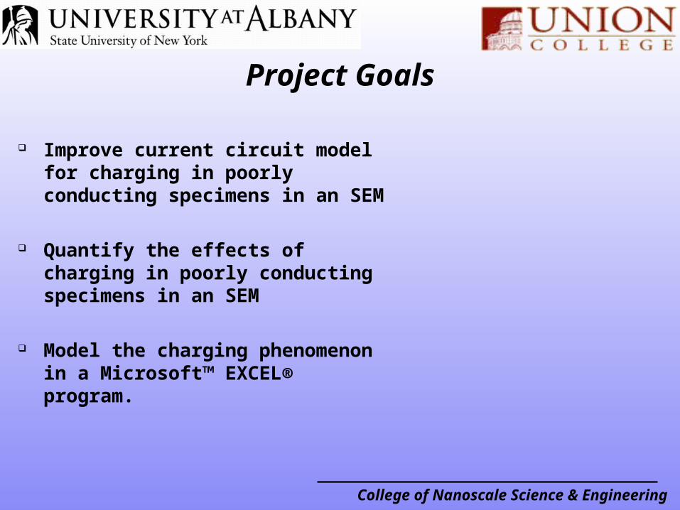
Results: Excel Program The curve is extended between the charging time and just before the
discharging takes place to emphasize the charging curve
The value of ∫δ(E) reaches a maximum value which restricts any excess charging on the sample

College of Nanoscale Science & Engineering
Future Plans
Improve model• Replace the potentiometer with an equivalent circuit• Calculate specific values for inputs• Test inputs against
Make program more useable • Cosmetic additions
Other platforms

College of Nanoscale Science & Engineering
References
SEM Movie – Oxford instruments Transistor Image – CNSE Metrology Dept Charge Density Pictures – Charging Effects in Scanning Electron
Microscopy – Shaffner Excel - Microsoft Corporation Multisim - Electronics Workbench Corporation.

College of Nanoscale Science & Engineering
Questions?