Embed Size (px)
Citation preview

Nagarajan et al., International Journal of Advanced Engineering Technology E-ISSN 0976-3945
Int J Adv Engg Tech/Vol. VII/Issue I/Jan.-March.,2016/258-263
Research Paper CLOSED LOOP OPERATION OF SVPWM BASED FOUR LEG
FAULT TOLERANT INVERTER FOR INDUSTRIAL APPLICATIONS
Dr. S. Nagarajan1*, P.Saradha Devi2 Address for Correspondence
Department of Electrical and Electronics Engineering, Jerusalem College of Engineering, Chennai, India ABSTRACT Induction motor drives are widely used in industrial applications. Inverter fed AC motor drives are sensitive to different faults. The occurrence of fault is due to failure of power switches used in the inverter. This may lead to interruption in the operation of drive system. It is essential to develop a fault detection and isolation technique to overcome the effect of fault and to supply uninterrupted power to the drive system. In this paper, a new fault detection and isolation method is proposed. In this method, the voltage source inverter is operated with four leg topology. The fourth leg in the inverter will serve as an auxiliary leg during faulty condition. If any one of the leg fails, the leg swap module in the driver circuit senses the fault and replaces the faulty leg with auxiliary leg. Once the fault is cleared, the leg swap module disconnects the auxiliary leg and connects the healthy leg to the inverter. This method provides a better compensation for inverter during faulty condition. This fault tolerant inverter is simulated using MATLAB/SIMULINK. To check the performance of the fault tolerant inverter, open circuit fault is introduced. The current and voltage waveforms are captured. From the simulation results, it is inferred that the performance of fault tolerant inverter replicates the performance of healthy VSI. The hardware implementation of fault tolerant VSI is done and the results are validated with simulation results.
I INTRODUCTION Induction motor drives are used in most of the industrial applications. The induction motor is fed by Voltage Source Inverter. The major drawback of inverter is failure of power switches which degrades the performance of induction motor drives. The failure of switches is due to two types of fault i.e., open circuit fault and short circuit fault. Open circuit fault is due to fault in gate drive or break of bond wires in MOSFET. Short circuit fault is due to malfunctioning of gate drive or permanent damage of MOSFET. So fault tolerant scheme is proposed to overcome the effect of fault in this paper.
Figure 1. Proposed System
In order to improve the performance of inverter, Space vector modulation is used to generate PWM pulses to drive the gate of inverter switches. Hence overall efficiency of the system can be improved. 2 SPACE VECTOR MODULATION The ultimate goal for using SVM is to lower the switching losses, maximize the bus utilization, reduce harmonic content and to achieve precise control. Space vector modulation is a PWM control algorithm for multi-phase AC generation, in which the reference signal is sampled regularly. After each sample, non-zero active switching vectors adjacent to the reference vector and one or more of the zero switching vectors are selected for the appropriate fraction of the sampling period in order to synthesize the reference signal as the average of the used vectors. In Space vector Modulation (SVPWM), a rotating phase voltage is obtained by adding all the three voltages. This Modulation is accomplished by switching state of an inverter. The three phase voltages are Va(t), Vb(t), Vc (t) . In the SVPWM scheme, the three phase output voltage is represented
by a reference vector which rotates at an angular speed of ω.
Figure 2. Space Vector Representation
From the figure 2, it is inferred that there are combinations of switching states to approximate the locus of Vref, the eight possible switching states of the inverter are represented as two null vector vectors and six active vectors. The three phase voltage system can be represented as vectors. This is done by transforming it into two phase co-ordinates. The formulae is given below,
= x ...........(1)
The reference vector Vref can be computed from the two phase co-ordinates Vα and Vβ.For a given magnitude and position Vref, can be synthesized by three nearby stationary vectors, based on which, the switching states of the inverter can be selected and gate signals for the active switches can be generated. When Vref, passes through sectors one by one, different sets of switches will be turned on and off . Hence the switching pattern varies for each sector. As a result, when Vref rotates one revolution in space, the inverter output voltage varies one cycle over time. The switching time states of the inverter can be computed from the formulae given below, Ta = Ts* Vs *sin(pi/3 – θ)/ 2* Vdc *sin(pi/3) ..(2) Tb= Ts* Vs* sin θ/ 2*Vdc*sin(pi/3) ..(3) To= Ts – T1- T2, .,(4)
Where Ts – Sampling period.
Figure 3.Switching Sequence of Vref in sector1

Nagarajan et al., International Journal of Advanced Engineering Technology E-ISSN 0976-3945
Int J Adv Engg Tech/Vol. VII/Issue I/Jan.-March.,2016/258-263
3 SIMULATION RESULTS 3.1 Simulation of SVPWM based VSI under healthy condition The simulink model of SVPWM based VSI is shown in figure 4. The rectifier converts AC to DC
according to the DC link requirement of the inverter. The DC voltage of about 415V is fed to the inverter through capacitor filter. The gates of the inverter are driven by SVPWM pulses.
Figure 4. Simulink model of SVPWM based VSI
3.2 Space Vector Modulator The Simulink model of Space vector modulator is shown in figure 5. The SIMULINK Implementation of the Space Vector Modulator has been carried out in the following sequence:
Generation of 3 phase voltages Calculation of Vα and Vβ Calculation Vref and alpha
Calculation of Ta, Tb, T0 Calculation of sector value Determination of switching states Realization of switching states Derivation of 6 individual gate pulses to two
level inverter
Figure 5. Simulink model of Space Vector Modulator
The generated gate pulses are used to trigger the MOSFET switches in the inverter. The line current waveforms and line current spectrum are shown in figure 6 and 7. From the results, it is inferred that line current for each phase is displaced by 120 ̊with each other.
Figure 6. Line Current waveform of SVPWM based
VSI under healthy condition
Figure 7. Line Current spectrum of SVPWM based VSI
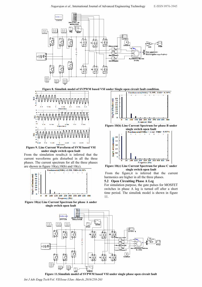
under healthy condition From figure 7, it is inferred that the THD value for all the three phases is 1.70%. Hence the current harmonics are considerably reduced when compared to other PWM techniques. 5 FAULT ANALYSIS 5.1 Open Circuiting Upper Leg of Phase A For simulation purpose, the gate pulses for MOSFET switch in upper leg of phase A is opened at time instant of 2ms. The Simulink model is shown in figure 8.The Current waveforms for three phases under fault condition are shown in figure 8.The current spectrum for three phases under faulty condition are shown in figure 9.
Nagarajan et al., International Journal of Advanced Engineering Technology E-ISSN 0976-3945
Int J Adv Engg Tech/Vol. VII/Issue I/Jan.-March.,2016/258-263
Figure 8. Simulink model of SVPWM based VSI under Single open circuit fault condition.
Figure 9. Line Current Waveform of SVM based VSI
under single switch open fault From the simulation results,it is inferred that the current waveforms gets disturbed in all the three phases. The current spectrum for all the three phases are shown in figure 10(a),10(b) and 10(c).
Figure 10(a) Line Current Spectrum for phase A under
single switch open fault
Figure 10(b) Line Current Spectrum for phase B under
single switch open fault
Figure 10(c) Line Current Spectrum for phase C under
single switch open fault From the figure,it is inferred that the current harmonics are higher in all the three phases. 5.2 Open Circuiting Phase A Leg For simulation purpose, the gate pulses for MOSFET switches in phase A leg is turned off after a short time period. The simulink model is shown in figure 11.
Figure 11.Simulink model of SVPWM based VSI under single phase open circuit fault

Nagarajan et al., International Journal of Advanced Engineering Technology E-ISSN 0976-3945
Int J Adv Engg Tech/Vol. VII/Issue I/Jan.-March.,2016/258-263
Figure 12. Line current waveform of SVPWM based VSI under single phase open circuit fault
The gate pulses for the switches in phase A leg is turned off after 2 secs. Since phase A leg is completely opened, the line current of phase A becomes zero. The current of other two phases gets
increased. The line current waveform is shown in figure 12. The line current spectrum for all the three phases is shown in figure 13(a),13(b)&13(c).
Figure 13a)Line Current Spectrum for phase A under
single phase open circuit fault Figure 13(b)Line Current Spectrum for phase B under
single phase open circuit fault
Figure 13(c) Line Current Spectrum for phase C under single phase open circuit fault
From the current spectrum, it is inferred that the phase A THD value is drastically increased to 194.07%. The Phase B and C is also disturbed. 6 CLOSED LOOP OPERATION OF FAULT TOLERANT INVERTER
The simulink model of four leg fault tolerant inverter is shown in figure 14. The simulation circuit comprises of rectifier, dc link, inverter and a leg swap module.
Figure 14. Simulink model of Closed loop operation of SVPWM based fault tolerant inverter

Nagarajan et al., International Journal of Advanced Engineering Technology E-ISSN 0976-3945
Int J Adv Engg Tech/Vol. VII/Issue I/Jan.-March.,2016/258-263
Figure 15. Leg Swap Module
The leg swap module consists of an auxiliary leg, phase identifier, circuit breaker and a comparator. The leg swap module is shown in figure 15. Auxiliary Leg: The auxiliary leg comprises of additional two switches. It serves as a fourth leg to the inverter under fault condition. Comparator: The comparator senses the line current of the inverter and gives the control signal to circuit breaker to disconnect the faulty leg and connect the auxiliary leg. Phase identifier: The phase identifier identifies the faulty leg. When fault occurs, the input to pulse identifier block is 1.The output will be the respective phase number. The line current waveform is shown in figure 16.
Figure 16. Line current waveform of fault tolerant
inverter under open circuit fault condition The line current spectrum of fault tolerant inverter is shown in figure 17.
Figure 17. Line Current spectrum of four leg topology
under open circuit fault condition From the simulation results, the performance of fault tolerant inverter is similar to VSI under healthy condition.
7 HARDWARE RESULTS The hardware setup comprises of power circuit, controller circuit and a driver circuit. An embedded C program is written and fed to the controller which generates pulses. The pulses are given to the driver unit and are amplified and used to trigger the switches in the power circuit. Two separate switches form an auxiliary switch, which can be used when any one leg of the healthy inverter fails. Induction motor load is used for testing the hardware and the output voltage waveforms are captured. The hardware setup is shown in figure 18.
Figure 18. Hardware setup
The auxillary leg is connected to the inverter during faulty condition by using thumb wheel switches under faulty condition.The line voltage, phase voltage and current waveforVSI are shown in figure 19(a), 19(b) and 19(c).
Figure 19(a). Line voltage waveform under healthy
condition(X axis 1cm = 5ms, Yaxis 1cm=100V)
Figure 19(b). Phase voltage waveform under healthy
condition(X axis 1cm = 5ms, Yaxis 1cm=100V)
Figure 19(c). Current waveform under healthy condition(X axis 1cm= 20ms, Y axis 1cm= 1A)

Nagarajan et al., International Journal of Advanced Engineering Technology E-ISSN 0976-3945
Int J Adv Engg Tech/Vol. VII/Issue I/Jan.-March.,2016/258-263
Hence the line voltage and phase voltage is obtained for healthy inverter.To check the performance of fault tolerant inverter,the pulses for phase A leg is turned off and the auxillary leg is connected to the inverter.The line voltage, phase voltage and current waveform of fault tolerant inverter is obtained and shown in figure 20(a),20(b) and 20(c).
Figure 20(a). Line voltage waveform of fault tolerant
condition under faulty condition (X axis 1cm = 5ms, Yaxis 1cm=100V)
Figure 20(b). Phase voltage waveform of fault tolerant
condition under faulty condition (X axis 1cm = 5ms, Yaxis 1cm=100V)
Figure 20(c). Current waveform of fault tolerant
condition under faulty condition (X axis 1cm= 20ms, Y axis 1cm= 1A)
Hence from the results obtained ,it is inferred that the performance of fault tolerant inverter is same as the healthy inverter. 8 CONCLUSION A fault tolerant scheme has been proposed for induction motor drive in closed loop operation. The system has advantages such as more reliable, affordable and efficient. The SVPWM technique has additional advantages like minimized switching losses, full utilization of DC link and improved efficiency. The fault tolerant system senses the fault and recovers the fault to minimize the time lag. The performance of fault tolerant inverter is similar to healthy VSI. REFERENCES
1. Bekheira Tabbache, Mohammed Benbouzid, Abdelaziz Kheloui, Jean-Matthieu Bourgeot and Abdeslam Mamoune.2013.PWM Inverter-Fed induction Motor-Based Electrical Vehicles Fault-Tolerant control. IEEE, 8204-8209.
2. Jianghan Zhang, Jin Zhao, Dehong Zhou and Chengguang Huang.2014. High-Performance Fault Diagnosis in PWM Voltage-Source Inverters for Vector-Controlled Induction Motor Drives IEEE transaction on Power electronics, Vol.29, No.11, PP.6087-6099.
3. Jorge F. Marques, Jorge O. Estima, Natalia S. Gemeiro and Antonio J.Marques Cardoso.2013 A New Diagnostic Technique for Real –Time Diagnosis of Power Converter Faults in Switched Reluctance Motor Drives. IEEE transaction on industry application, Vol.50, No.3, PP.1854 – 1860.
4. Jose A. Restrepo, Alberto Berzoy, Antonio E. Ginart, Jose M. Aller, Ronald G. Harley and Thomas G.Habetler.2012.Switching Strategies for fault Tolerant Operation of Single DC-Link Dual Convertors. IEEE transaction Vol.27, No.2, PP.509-518.
5. Kui-Jun Lee, Nam-JU park, Kyung-Hwan Kim and Dong-Seok Hyun. Simple Fault Detection and Tolerant Scheme in VSI-Fed Switched Reluctance Motor. on IEEE transaction.
6. Nagarajan.S and Rama Reddy.S Fault Analysis on VSI Fed Induction Motor Drive with Fault Tolerant Strategy . Research journal of Applied Sciences, Engineering and Technology, PP.2004-2016.
7. Natalia S. Gameiro and Antonio J.Marques Cardoso.2012A New Method for Power Converter Fault Diagnosis in SRM Drives. IEEE transaction on Industry applications, Vol.48, No.2, PP.653-662.
8. Nuno M. A. Freire, Jorge O. Estima, A. J. Marques Cardoso.2014.A Voltage-Based approach without extra hardware for Open-Circuit Fault Diagnosis in Closed-Loop PWM AC Regenerative Drives. IEEE transaction on industrial electronics, Vol.61, No.9, PP.4960-4970..
9. Rammohan Rao Errabelli and Peter Mutschler.2012.Fault-Tolerant Voltage Source Inverter for Permanent magnet drives IEEE transaction on power electronics Vol.27, No.2, PP.500-508.
10. Shin-Myung Jung, Jin-Sik Park, Hag-Wone Kim, Kwan-Yuhl Cho and Myung-Joong Youn.2013.An MRAS-Based Diagnosis of Open –Circuit Fault in PWM Voltage-Source Inverters for PM Synchronous Motor Drive Systems. IEEE transaction on Power electronics, Vol.28, No.5, PP.2514-2526.
11. Teresa Orlowska-Kowalska and Piotr Sobanski.2013.Simple Sensorless Diagnosis Methos for Open-Switch Faults in SVM-VSI-Fed Induction Motor Drive. IEEE transaction, PP.8210-8215.
![A Comparative Study and Experimental Investigation of ...SVPWM, who contributed a lot in PWM methods [4-9]. In comparison between SPWM and SVPWM, SVPWM results excellent dc bus utilization](https://img.dokumen.tips/doc/110x75/61264de56b3f754d585eb80a/a-comparative-study-and-experimental-investigation-of-svpwm-who-contributed.jpg)