Embed Size (px)
Citation preview

International Journal of Engineering and Technology Volume 1 No. 1, October, 2011
Copyright IJET © 2011 - IJET Publications UK
APPLICATION OF SVPWM TECHNIQUE TO THREE LEVEL
VOLTAGE SOURCE INVERTER
1JBV Subrahmanyam,
2Sankar
1Electrical & Electronics Engineering Dept.,Bharat Institute of Engineering &Technology, mangalpally, ibrahimpatnam,
RR district, Hyderabad,AP,INDIA 501 510 2Electrical & Electronics Engineering Dept Holymary institute of technology&science,kesara, RR district,
Hyderabad,AP,INDIA Email: [email protected], [email protected]
ABSTRACT
The purpose of the study is to compute the Total Harmonic Distortion (THD) with the proposed latest Space Vector Pulse
Width Modulation(SVPWM) technique and prove that the proposed technique gives lesser THD compared to that of
Sinusoidal PWM.Multilevel inversion is a power conversion strategy in which the output voltage is obtained in steps thus
bringing the output closer to a sine wave and reduces the Total Harmonic Distortion (THD). Multilevel inverter structures have
been developed to overcome shortcomings in solid-state switching device ratings so that they can be applied to higher voltage
systems. The multilevel Voltage Source Inverter (VSI) unique structure allows them to reach high voltages with low harmonics
without the use of transformers. The general function of the multilevel inverter is to synthesize a desired ac voltage from
several levels of dc voltages. In recent years, the multilevel inverters have drawn tremendous interest in the area of high-power
medium-voltage energy control. Three different topologies have been proposed for multilevel inverters like Diode-Clamped
Inverter (DCI), Capacitor Clamped Inverter (CCI) and Cascaded Multicell Inverter (CMI). The DCI is also called the Neutral-
Point Clamped (NPC) inverter, when it was first used in a three-level inverter in
which the mid-voltage level was defined as the neutral point. CCI is also called Flying Capacitor Inverter (FCI) and cascaded
multicell is combination of individual small voltage sources, with separated dc sources. In addition, several modulation and
control strategies have been developed or adopted for multilevel inverters including multilevel Sinusoidal
Pulse Width Modulation (SPWM), and Space Vector Modulation (SVM).
Key words: Total Harmonic Distortion, Sinusoidal PWM, Space Vector Pulse Width Modulation(SVPWM), Voltage Source Inverter (VSI)
1. INTRODUCTION
Inversion is the conversion of DC power to AC
power at a desired output voltage or current and frequency.
A static semiconductor inverter circuit performs this
electrical energy inverting transformation. The terms
voltage-fed and current-fed are used in connection with the
output from inverter circuits. A Voltage Source Inverter
(VSI) is the one in which DC input voltage is essentially
constant and independent of the load current drawn. The
inverter specifies the load voltage while the drawn current
shape is dictated by the load.
The DC power input to the inverter is obtained
from an existing power supply network (or) from a
rotating alternator through a rectifier (or) a battery, fuel
cell, photo voltage array (or) Magneto Hydro Dynamic
(MHD) generator.
Inverters are mainly classified as Voltage Source
Inverters (VSI) and Current Source Inverters (CSI). A VSI
is the one in which the DC source has small or negligible
impedance. In other words, a VSI has stiff DC voltage
source at its terminals. Because of low internal impedance,
the terminal voltage of a VSI remains substantially
constant with variations in load. It is therefore equally
suitable to single motor and multi-motor drives. Any short
circuit across its terminals causes current to rise very fast,
due to the low time constant of its internal impedance. The
fault current cannot be regulated by current control and
must be cleared by fast acting fused links.
On the other hand, the CSI is supplied with a
control current from a DC source of high impedance.
Typically a phase control thyristor rectifier feeds the
inverter with a regulated current through a large series
inductor. Thus load current rather than load voltage is
controlled and the inverter output voltage is dependent
upon the load impedance. Because of large internal
impedance, the terminal voltage of a CSI changes
substantially with a change in load. Therefore, if used in a
multi-motor drive, a change in load on any motor affects
other motors. Hence, CSIs are not suitable for multi-motor
drives.
MATERIALS AND METHODS
This study was conducted in 2011 in the Electrical
&Electronics Engineering Department of Bharat Institute
of Engineering & Technology, Mangalpally,
Hyderabad,AP, India

International Journal of Engineering and Technology Volume 1 No. 1, October, 2011
Copyright IJET © 2011 - IJET Publications UK
2. MULTILEVEL INVERTERS AND
MODULATING TECHNIQUES
2.1 Pulse Width Modulation(PWM) Techniques
A power electronic inverter is essentially a device
for creating a variable AC magnitude and frequency output
from a DC input. The frequency of the output voltage or
current is readily established by simply switching for equal
time periods to the positive and negative DC bus and
appropriately adjusting the half cycle period. However the
variable frequency ability is accompanied by a
corresponding need to adjust the amplitude of fundamental
component of the output waveform as the frequency
changes i.e., voltage control. One of the widely utilized
strategies for controlling the AC output of power
electronic converters is the PWM [4] Technique. This
varies the duty cycle of the inverter switches at a high
frequency to achieve a target average low-frequency
output voltage or current.
Modulation theory has been a major research area
in power electronics for over three decades and continues
to attract considerable attention and interest. On the other
hand, there have been a number of clear trends in the
development of PWM concepts and strategies since 1970s,
addressing the main objectives of reduced harmonic
distortion and increased output magnitudes for a given
switching frequency and the development of modulation
strategies to suit different converter topologies.
Principle of PWM
Fig. 2.1 illustrates the circuit model of a single-
phase inverter with a center-tapped grounded DC bus and
Fig. 2.2 illustrates the principle of PWM.
Fig. 2.1 Circuit Model of Single - Phase Inverter
Fig. 2.2 Pulse Width Modulation(PWM)
From Fig. 2.2 the inverter output voltage is determined in
the following
1. When , = /2
2. When , = /2
M= , ………(1)
……..(2)
3. MODULATION TECHNIQUES FOR
DIODE CLAMPED MULTILEVEL
INVERTER
3.1 Third Harmonic Injected PWM
The reference ac waveform is not sinusoidal as
illustrated in Fig. 3.1 but consists of both fundamental
component and a third harmonic component. As a result,
the resulting peak to peak amplitude of the resulting
reference function does not exceed the dc supply voltage
, but the fundamental component is higher than the
available supply . The presence of exactly the same
third harmonic component in each phase results in an
effective cancellation of the third harmonic component at
the neutral terminal and all sinusoidals with peak
amplitude. This is approximately 15.5% higher in
amplitude than that achieved by the sinusoidal PWM.
Therefore, the third harmonic PWM provides better
utilization of the dc supply voltage.

International Journal of Engineering and Technology Volume 1 No. 1, October, 2011
Copyright IJET © 2011 - IJET Publications UK
Fig. 3.1 Third Harmonic Injected PWM with Triangular
Carriers for Multilevel Inverter
4. SPACE VECTOR MODULATION
(SVM)
4.1 INTRODUCTION
The space vector constituted by the pole voltages ,
and is defined as:
= + .exp [j (2π/3)] + .exp [j (4π/3)]…(3)
The relationship between the phase voltages , ,
and pole , and is given by:
= + ;…..(4)
= + ;…….(5)
= + ;……(6)
Since + + =0;
= ( )/3 …..(7)
Where is the common mode voltage
From Eqns. (4), (5) and (6) it is evident that phase voltages
, , also result in the same space vector .
The space vector can also be resolved into two
rectangular components namely and as in Eqn. (7).
It is customary to place the α-axis along the A-phase axis
of the motor.
Hence:
= +j …….(8)
4.2 PRINCIPLE OF SPACE VECTOR
MODULATION
An inverter is now-a-days commonly used in
variable speed ac motor drives to produce a variable, three
phase ac output voltage from a DC voltage. Since AC
voltage is defined by two characteristics, amplitude and
frequency, it is essential to work out a strategy that permits
control over both these quantities. PWM controls the
average output voltage in a sufficiently small period,
called switching period, by producing pulses of variable
duty-cycles [3]. Here, sufficiently small means the
switching is small compared to the desired output voltage
which may be considered as equal to desired.
Fig. 4.1 Three-phase two-level PWM inverter
= …(9)
Also, the relationship between switching variable
vector [a b c] t and line-line voltage vector [ ]
t
can be expressed in Eqn. (10)
= ……(10)
As illustrated in Fig. 4.2 there are eight possible
combinations of on and off patterns for the three upper
power switches [11]. The on and off states of the lower
power devices are opposite to the upper one and so are
easily determined once the states of the upper power
transistors are determined. According to Eqns.(4),(5),(6),
the switching vectors, output line to neutral voltage, and

International Journal of Engineering and Technology Volume 1 No. 1, October, 2011
Copyright IJET © 2011 - IJET Publications UK
output line-line voltages in terms of DC link are given
in table 4.1 and Fig. 4.2 shows the eight inverter voltage
vectors ( to )
Table 4.1 Switching vectors, line to neutral
voltages and line to line voltages
Voltage
Vector
Switching
Vectors
Line to neutral
voltage
Line to line
voltage
a b c
0 0 0 0 0 0 0 0 0
1 0 0 2/3 -1/3 -1/3 1 0 -1
1 1 0 1/3 1/3 -2/3 0 1 -1
0 1 0 -1/3 2/3 -1/3 -1 1 0
0 1 1 -2/3 1/3 1/3 -1 0 1
0 0 1 -1/3 2/3 2/3 0 -1 1
1 0 1 -2/3 1/3 1/3 1 -1 0
1 1 1 0 0 0 0 0 0
Fig. 4.2 Inverter voltages vectors ( to )
4.3 OPERATION OF THREE-PHASE
THREE-LEVEL INVERTER
Fig. 4.3 Power circuit for Three-phase three-level inverter
Fig. 4.3 illustrates the basic circuit for the three-level
DC3LI. The circuit employs 12 power switching devices
and 6 clamping diodes (D1-D6)and the DC bus voltage is
split into three-levels(+Vdc/2, 0,-Vdc/2). Thus, the voltage
stress of the switching device is greatly reduced. The
output phase voltage Vao has three different states: +Vdc/2,
0, -Vdc/2. Here take phase A as an e.g., for voltage. For
voltage +Vdc/2, Sa1 and Sa2 need to be turned on. We can
define these states as 2, 1, and 0, respectively [12].The
switching variable Sa in table 4.4 ,is similar to three-phase
two-level inverter, the switching states of each bridge leg
of three-phase three-level inverter is described by using
switching variables Sa, Sb and Sc.The difference is that, in
three-level inverter, each bridge leg has three different
switching states.
Table 4.4 Switching variables of phase A
Vao Sa1 Sa2 S'a2 S'a1 Sa
+Vdc/2 ON ON OFF OFF 2
0 OFF ON ON OFF 1
-Vdc/2 OFF OFF ON ON 0
Using switching variable Sa and DC bus voltage
Vdc, the output phase voltage Vao is obtained as follows:
Van=(Sa-1)*Vdc/2 ………(11)
And the output line voltage of phase A and B can be
expressed as follows:
Vab = Vao - Vbo = 1/2*Vdc (Sa-Sb).....(12)
4.4 SPACE VECTOR PWM FOR THREE
LEVEL INVERTER
There are altogether 27 switching states in a
DC3LI. They correspond to 19 voltage vectors whose
positions are fixed. These space voltage vectors can be
classified into four groups, where the first group
corresponds to 3 zero vectors or null vectors (V0, V7,
V14), the second group consists of large voltage vectors
(V15-V20), the third group consists of medium voltage
vectors (V8-V13) and finally the fourth group consists of
small voltage vectors (V1-V6). The last three groups can
be distinguished into three hexagons illustrated in Fig. 4.6.
Fig. 4.4 Space Vector hexagon
International Journal of Engineering and Technology Volume 1 No. 1, October, 2011
Copyright IJET © 2011 - IJET Publications UK
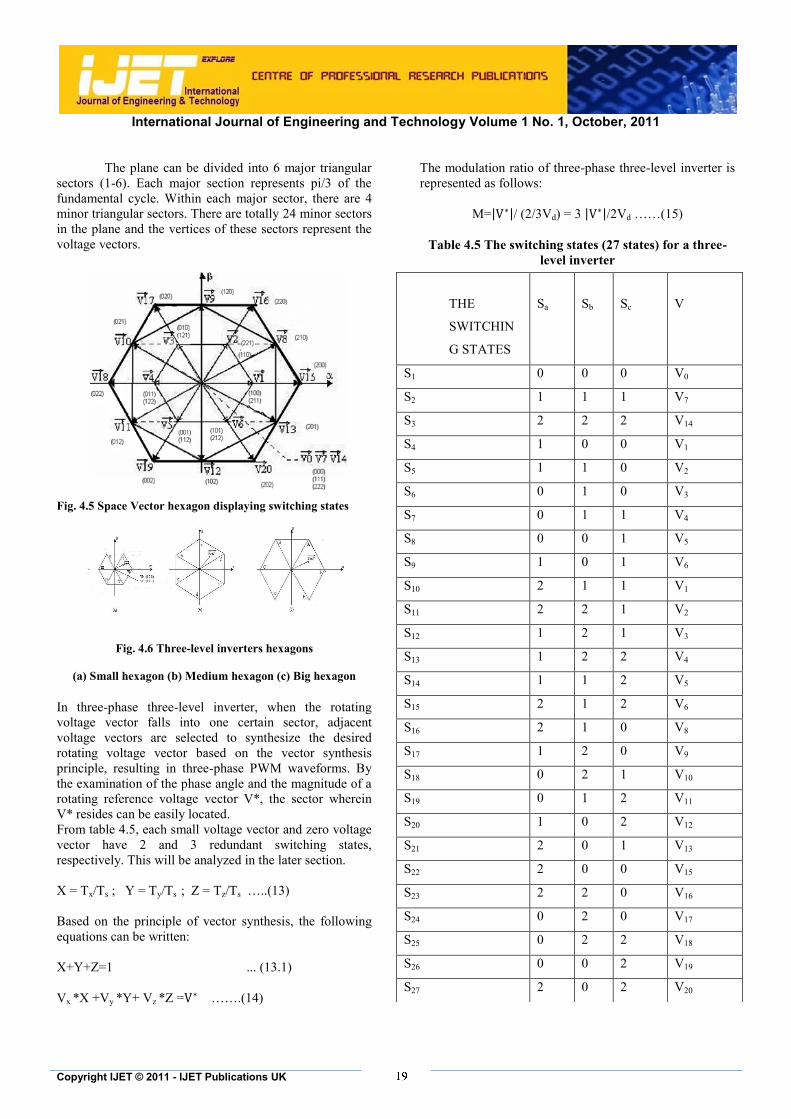
The plane can be divided into 6 major triangular
sectors (1-6). Each major section represents pi/3 of the
fundamental cycle. Within each major sector, there are 4
minor triangular sectors. There are totally 24 minor sectors
in the plane and the vertices of these sectors represent the
voltage vectors.
Fig. 4.5 Space Vector hexagon displaying switching states
Fig. 4.6 Three-level inverters hexagons
(a) Small hexagon (b) Medium hexagon (c) Big hexagon
In three-phase three-level inverter, when the rotating
voltage vector falls into one certain sector, adjacent
voltage vectors are selected to synthesize the desired
rotating voltage vector based on the vector synthesis
principle, resulting in three-phase PWM waveforms. By
the examination of the phase angle and the magnitude of a
rotating reference voltage vector V*, the sector wherein
V* resides can be easily located.
From table 4.5, each small voltage vector and zero voltage
vector have 2 and 3 redundant switching states,
respectively. This will be analyzed in the later section.
X = Tx/Ts ; Y = Ty/Ts ; Z = Tz/Ts …..(13)
Based on the principle of vector synthesis, the following
equations can be written:
X+Y+Z=1 ... (13.1)
Vx *X +Vy *Y+ Vz *Z = …….(14)
The modulation ratio of three-phase three-level inverter is
represented as follows:
M= / (2/3Vd) = 3 /2Vd ……(15)
Table 4.5 The switching states (27 states) for a three-
level inverter
THE
SWITCHIN
G STATES
Sa
Sb
Sc
V
S1 0 0 0 V0
S2 1 1 1 V7
S3 2 2 2 V14
S4 1 0 0 V1
S5 1 1 0 V2
S6 0 1 0 V3
S7 0 1 1 V4
S8 0 0 1 V5
S9 1 0 1 V6
S10 2 1 1 V1
S11 2 2 1 V2
S12 1 2 1 V3
S13 1 2 2 V4
S14 1 1 2 V5
S15 2 1 2 V6
S16 2 1 0 V8
S17 1 2 0 V9
S18 0 2 1 V10
S19 0 1 2 V11
S20 1 0 2 V12
S21 2 0 1 V13
S22 2 0 0 V15
S23 2 2 0 V16
S24 0 2 0 V17
S25 0 2 2 V18
S26 0 0 2 V19
S27 2 0 2 V20

International Journal of Engineering and Technology Volume 1 No. 1, October, 2011
Copyright IJET © 2011 - IJET Publications UK
Where is the magnitude of the reference
voltage vector , which rotates with an angular speed of
ω=2f in d-q coordinate plane and 2/3 Vdc is magnitude of
the large voltage vector, e.g., V13.states: + Vdc /2, 0, and -
Vdc /2
5. SIMULATION RESULTS AND
DISCUSSION
5.1 FOR A DIODE CLAMPED THREE-LEVEL
INVERTER
5.1.1. Sinusoidal Pulse Width Modulation (SPWM)
Fig. 5.1 Line Voltage of DC3LI with SPWM
Fig. 5.2 THD spectrum of DC3LI with SPWM
Fig. 5.1 illustrates the Line Voltage of DC3LI with
SPWM and Fig. 5.2 illustrates the THD spectrum of
DC3LI with SPWM.In this modulation technique the
fundamental voltage is 233.3 V and THD is 29.89%.
5.1.2 Space Vector Pulse Width Modulation
(SVPWM)
Fig. 5.3 Line Voltage of DC3LI with SVPWM
Fig. 5.4 THD spectrum of DC3LI with SVPWM
MODULTION
TECHNIQUES
DC3LI
THD Fundamental
Component
Sinusoidal PWM 29.95% 200.1 V
SVPWM 20.31% 173.1.7 V

International Journal of Engineering and Technology Volume 1 No. 1, October, 2011
Copyright IJET © 2011 - IJET Publications UK
Fig. 5.4 illustrates the Line Voltage of DC3LI with
SVPWM and the THD spectrum of DC3LI with SVPWM.
In this modulation technique, the fundamental voltage is
312.7 V and THD is 23.20%.
6. CONCLUSIONS AND FUTURE SCOPE
6.1 Conclusions
Diode Clamped Multi-Level Inverter topologies are
developed with 3-levels for various modulation techniques
i.e., Sinusoidal PWM, Space Vector PWM and DC3LI
topology. Space Vector PWM technique gives lesser THD
compared to that of Sinusoidal PWM.
6.2 Scope For Future Work
The presented simulink model can be setup
experimentally using semi conductor devices like
Transistor, Thyristor, MOSFET etc., and controlling
strategies by using any of the following devices like
microprocessor, microcontroller, digital signal processor
and FPGA. The controlling strategies can be implemented
using m-file programming with FPGA for better
processing speed and performance.
ACKNOWLEDGEMENT
Authors acknowledge the support, encouragement
and facilities provided by the Electrical&Electronics
Engineering Department and management of Bharat
Institute of Engineering & Technology
(BIET),Mangalpally, ibrahimpatnam,Hyderabad,AP, India
in carryout the presented study/research work.
REFERENCES
[1] R. Teodorescu, F. Beaabjerg, J. K. Pedersen, E.
Cengelci, S. Sulistijo, B. Woo, and P. Enjeti,
―Multilevel converters — A survey,‖ in Proc.
European Power Electronics Conf. (EPE’99),
Lausanne, Switzerland, 1999, CD-ROM.
[2] A. Nabae, I. Takahashi, and H. Akagi, ―A new
neutral-point clamped PWM inverter,‖ IEEE
Trans. Ind. Applications., vol. IA-17, pp. 518–
523, Sept./Oct. 1981.
[3] T. A. Meynard and H. Foch, ―Multi-level
choppers for high voltage applications,‖ Eur.
Power Electron. Drives J., vol. 2, no. 1, p. 41,
Mar.1992.
[4] C. Hochgraf, R. Lasseter, D. Divan, and T. A.
Lipo, ―Comparison of multilevel inverters for
static var compensation,‖ in Conf. Rec. IEEE-
IAS Annu. Meeting, Oct. 1994, pp. 921–928.
[5] P. Hammond, ―A new approach to enhance
power quality for medium voltage ac drives,‖
IEEE Trans. Ind. Applications., vol. 33, pp.
202–208, Jan./Feb. 1997.
[6] E. Cengelci, S. U. Sulistijo, B. O. Woom, P.
Enjeti, R. Teodorescu, and F. Blaabjerge, ―A
new medium voltage PWM inverter topology
for adjustable speed drives,‖ in Conf. Rec.
IEEE-IAS Annu. Meeting, St. Louis, MO, Oct.
1998, pp. 1416–1423.
[7] R. H. Baker and L. H. Bannister, ―Electric
power converter,‖ U.S. Patent 3 867 643, Feb.
1975.
[8] R. H. Baker, ―Switching circuit,‖ U.S. Patent 4
210 826, July 1980.
[9] ―Bridge converter circuit,‖ U.S. Patent 4 270
163, May 1981.
[10] P.W. Hammond, ―Medium voltagePWMdrive
and method,‖ U.S. Patent 5 625 545, Apr.
1997.
[11] F. Z. Peng and J. S. Lai, ―Multilevel cascade
voltage-source inverter with separate DC
sources,‖ U.S. Patent 5 642 275, June 24, 1997.
[12] P.W. Hammond, ―Four-quadrant AC-AC drive
and method,‖ U.S. Patent 6 166 513, Dec.
2000.
[13] M. F. Aiello, P. W. Hammond, and M. Rastogi,
―Modular multi-level adjustable supply with
series connected active inputs,‖ U.S. Patent 6
236 580, May 2001.
[14] RODRÍGUEZ et al.: MULTILEVEL
INVERTERS 737 ―Modular multi-level
adjustable supply with parallel connectedactive
inputs,‖ U.S. Patent 6 301 130, Oct. 2001.
AUTHOR’S BIOGRAPHY
Dr. JBV Subrahmanyam is a Doctorate in Electrical
Engineering from JNTU-Hyderabad, India, with two
decades of rich experience in teaching, training, research,
industry, projects and consultancy. He published 15
research papers in reputed international journals and 20
papers in international and national conferences.His
research interest is in automation of power systems. He is
an expert in condition monitoring of industrial equipment
through modern diagnostic techniques. He implemented

International Journal of Engineering and Technology Volume 1 No. 1, October, 2011
Copyright IJET © 2011 - IJET Publications UK
the latest GPS and GIS technologies in many power
utilities in India successfully. He executed many
international and national level technical projects
effectively funded by Power Finance Corporation,
Ministry of Power, Government of India, APDRP, DRUM,
USAID and DFID-UK.
Mr. Sankar is a faculty in electrical engineering
department of HITS, Hyderabad, India, with many years of
rich experience in teaching, training, research. His
research interest is in automation of power systems.