Embed Size (px)
Citation preview

Clock Routing

CAD for VLSI 2
Problem Formulation
• Specialized algorithms are required for clock (and power nets) due to strict specifications for routing such nets.– Better to develop specialized routers for these nets.– Do not over-complicate the general router.– In many designs, both these nets are manually routed.
• Sophisticated and accurate clock routing tools are a must for high-performance designs.
CAD for VLSI 3
Clock Routing
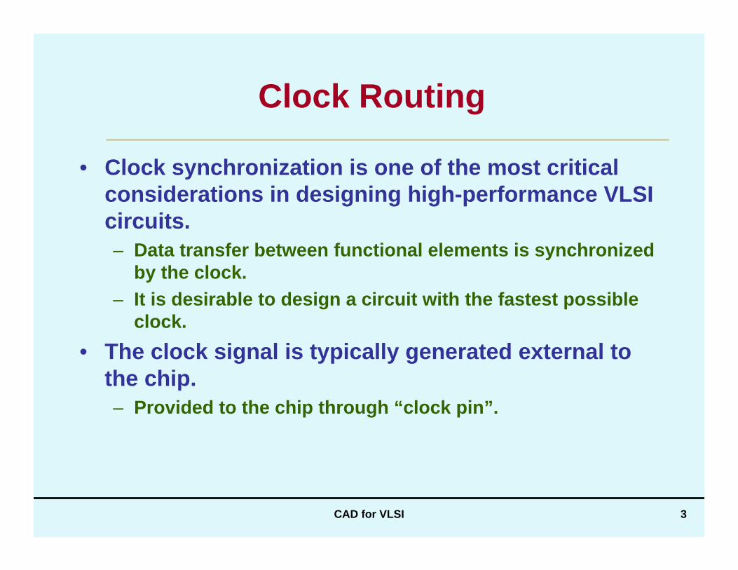
• Clock synchronization is one of the most critical considerations in designing high-performance VLSI circuits.– Data transfer between functional elements is synchronized
by the clock.– It is desirable to design a circuit with the fastest possible
clock.• The clock signal is typically generated external to
the chip.– Provided to the chip through “clock pin”.
CAD for VLSI 4
Contd.
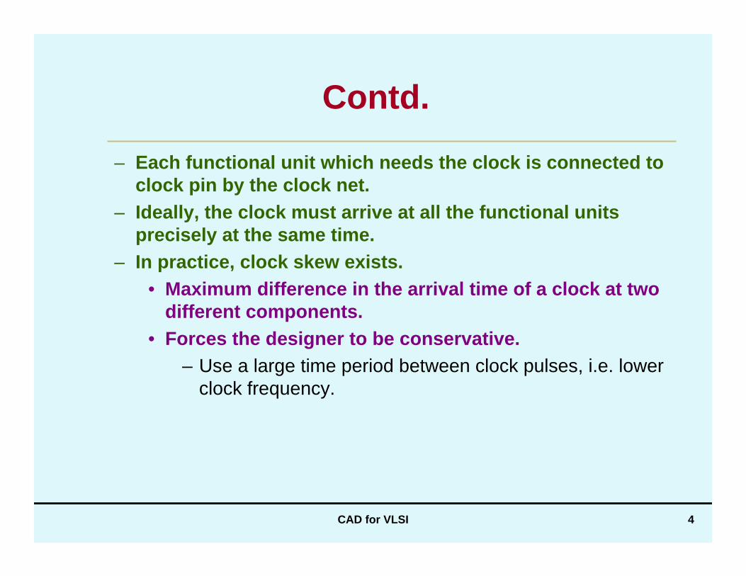
– Each functional unit which needs the clock is connected to clock pin by the clock net.
– Ideally, the clock must arrive at all the functional units precisely at the same time.
– In practice, clock skew exists.• Maximum difference in the arrival time of a clock at two
different components.• Forces the designer to be conservative.
– Use a large time period between clock pulses, i.e. lower clock frequency.
CAD for VLSI 5
Clocking Schemes
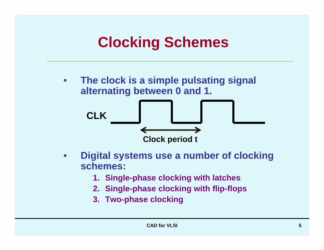
• The clock is a simple pulsating signal alternating between 0 and 1.
• Digital systems use a number of clocking schemes:
1. Single-phase clocking with latches2. Single-phase clocking with flip-flops3. Two-phase clocking
Clock period t
CLK

CAD for VLSI 6
Single-phase Clocking with Latches
• The latch opens when the clock goes high.• Data are accepted continuously while the clock is
high.• The latch closes when the clock goes down.• Not commonly used due to their complicated timing
requirements.– Some high-performance circuits use this scheme.
LD
CLKQ

CAD for VLSI 7
Single-phase Clocking with Flip-flops
• Data are accepted only on the rising or falling edge of the clock.
FFD
CLKQ
CAD for VLSI 8
Two-phase Clocking
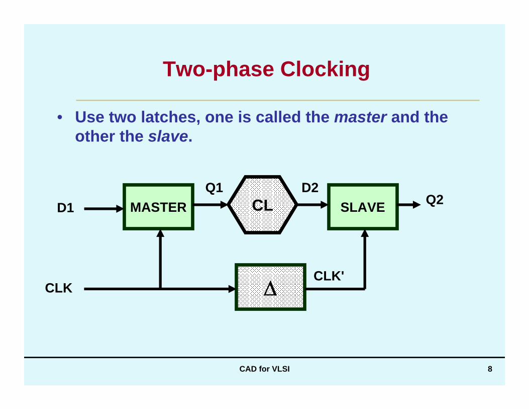
• Use two latches, one is called the master and the other the slave.
MASTER SLAVECL
ΔCLK'
Q2D2
D1Q1
CLK
CAD for VLSI 9
Clocking Schemes:: Contd.
• As a rule of thumb, most systems cannot tolerate a clock skew of more than 10% of the system clock period.– A good clock distribution strategy is necessary.– Also a requirement for designing high-performance
circuits.

CAD for VLSI 10
Clock Buffering Mechanisms
• Clock signal is global in nature.– Clock lines are typically very long.– Long wires have large capacitances, which limit the
performance of the system.– RC delay plays a big factor.
• RC delay cannot be reduced by making the wires wider.– Resistance reduces, but capacitance increases.
• To reduce RC delay, buffers are used.– Also helps to preserve the clock waveform.– Significantly reduces the delay.– May occupy as much as 5% of the total chip area.

CAD for VLSI 11
Clock Buffering:: Approach 1
• Use a big, centralized buffer.– Better from skew minimization point of view.
CAD for VLSI 12
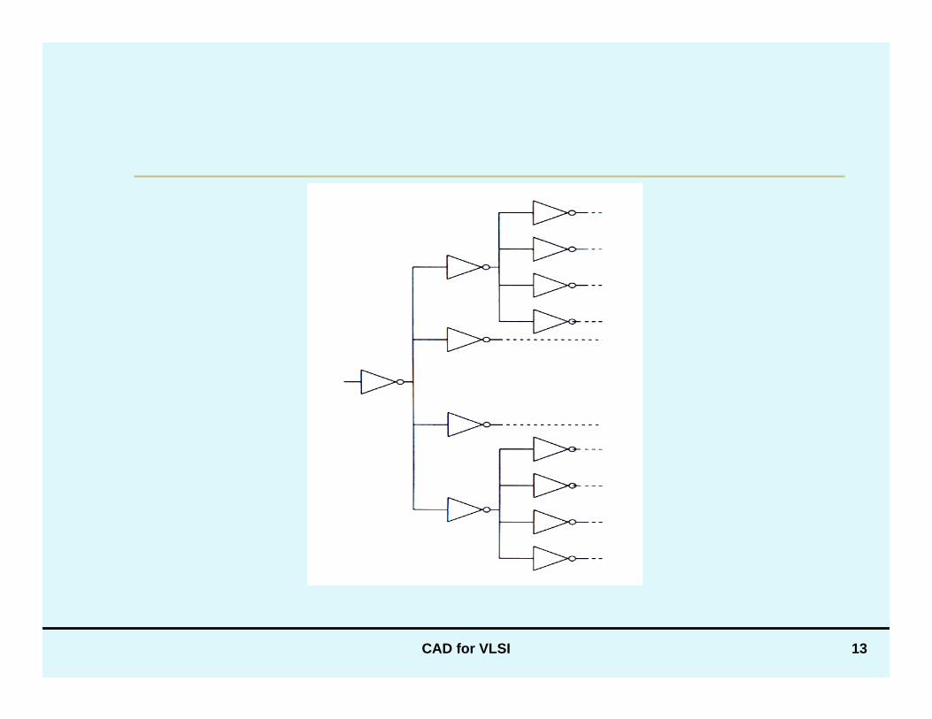
Clock Buffering:: Approach 2
• Distribute buffers in the branches of the clock tree.– Use identical buffers so that the delay introduced by the
buffers is equal in all branches.• Regular layout of the clock tree, and equalization of
the buffer loads help to reduce clock skew.
CAD for VLSI 13
CAD for VLSI 14
Clock Routing Algorithms
• How to minimize skew?– Distribute the clock signal in such a way that the
interconnections carrying the clock signal to functional sub-blocks are equal in length.
• Several clock routing algorithms exist which try to achieve this goal.– H-tree based algorithm– X-tree based algorithm– MMM algorithm– Weighted center algorithm– Zero clock skew routing

CAD for VLSI 15
H-tree based Algorithm
• Consider that all clock terminals are arranged in a symmetrical fashion, as in the case of gate arrays.

CAD for VLSI 16
Contd.
– In (a), all points are exactly 7 units from the point P0, and hence the skew is zero.
– This ensures minimum-delay routing as well.• P0 and P3 are at a distance 7 (rectilinear distance).
– Can be generalized to n points, where n is a power of 4.

CAD for VLSI 17
X-tree based Algorithm
• An alternate tree structure with a smaller delay.– Assuming non-rectilinear routing is possible.
• Although apparently better than H-trees, this may cause crosstalk due to close proximity of wires.
• Like H-trees, this is also applicable for very special structures.– Not applicable in general.

CAD for VLSI 18
Contd.

CAD for VLSI 19
Method of Means & Medians (MMM)
• Follows a strategy very similar to the H-tree algorithm.– Recursively partition a circuit into two equal parts.– Connects the center of mass of the whole circuit to the
centers of masses of the two partitioned sub-circuits.
CAD for VLSI 20
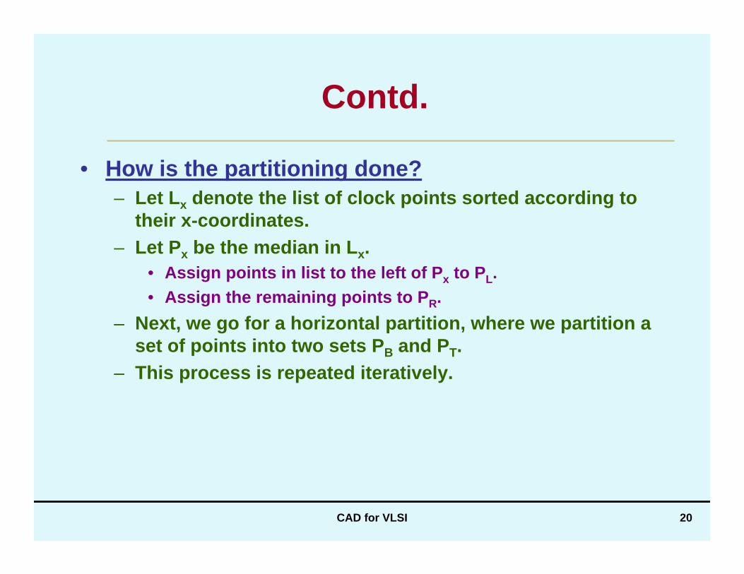
Contd.
• How is the partitioning done?– Let Lx denote the list of clock points sorted according to
their x-coordinates.– Let Px be the median in Lx.
• Assign points in list to the left of Px to PL.• Assign the remaining points to PR.
– Next, we go for a horizontal partition, where we partition a set of points into two sets PB and PT.
– This process is repeated iteratively.

CAD for VLSI 21
Contd.
• The basic algorithm ignores the blockages and produces a non-rectilinear tree. Some wires may also intersect.– In the second phase, each wire can be converted so that it
consists only of rectilinear segments and avoids blockages.

CAD for VLSI 22

CAD for VLSI 23
Zero Skew Clock Routing
• Based on the Elmore delay model.– Delay along an edge is proportional to its length.– However, the delay along a path is defined recursively.
• The point set is recursively partitioned into two subsets, and trees are constructed in a bottom-up manner.– Assume, inductively, that every sub-tree has achieved zero
skew.– Given two zero-skew sub-trees, merge them by an edge to
achieve zero skew on the new tree.• Necessary to decide the position of the connecting
points (taps).• Uses Elmore delay model for the purpose.

Power and Ground Routing
CAD for VLSI 25
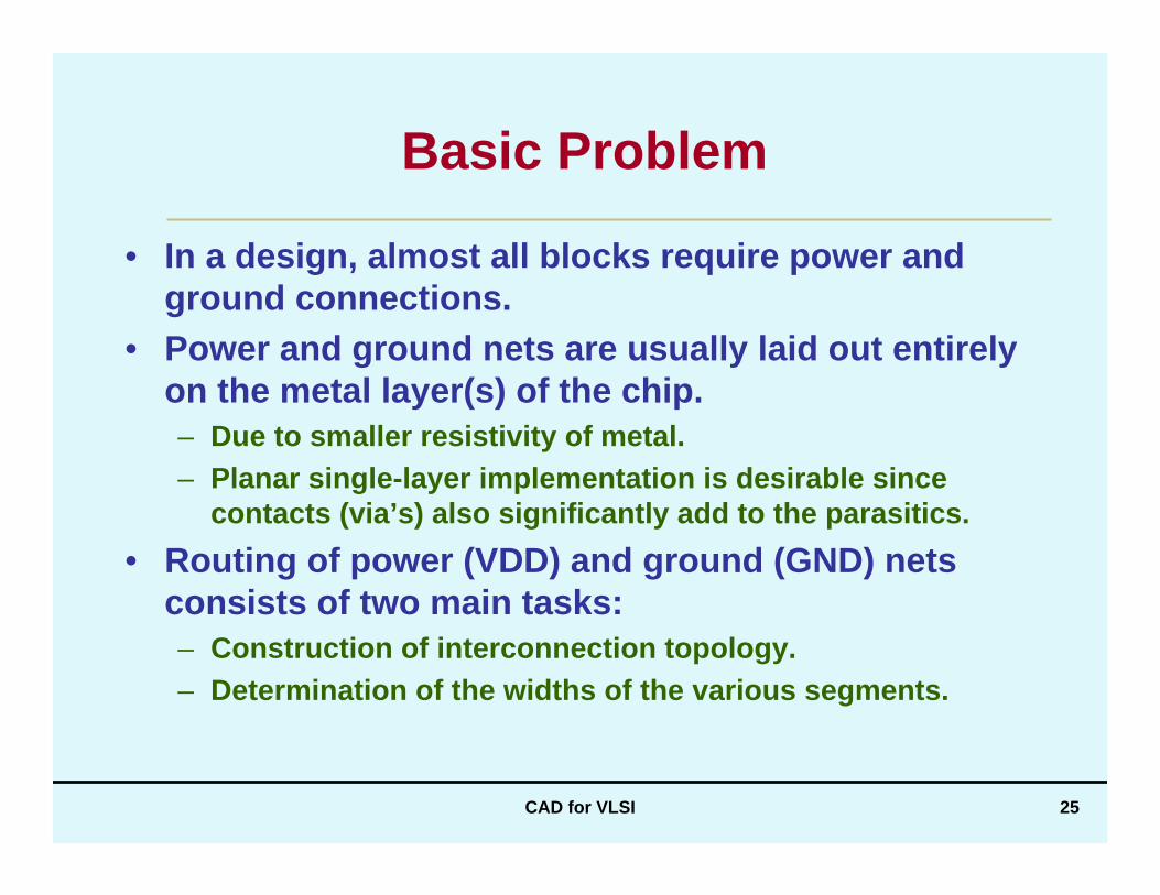
Basic Problem
• In a design, almost all blocks require power and ground connections.
• Power and ground nets are usually laid out entirely on the metal layer(s) of the chip.– Due to smaller resistivity of metal.– Planar single-layer implementation is desirable since
contacts (via’s) also significantly add to the parasitics.• Routing of power (VDD) and ground (GND) nets
consists of two main tasks:– Construction of interconnection topology.– Determination of the widths of the various segments.

CAD for VLSI 26
Contd.
• Requirement:– Find two non-intersecting interconnection trees.– The width of the trees at any particular point must be
proportional to the amount of current being drawn by the points in that sub-tree.

CAD for VLSI 27
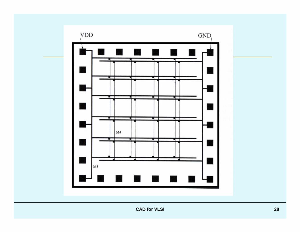
Approach 1:: Grid Structure
• Several rows of horizontal wires for both VDD and GND run parallel to each other on one metal layer.
• The vertical wires run in another metal layer and connect the horizontal wires.
• A block simply connects to the nearest VDD and GND wire.
CAD for VLSI 28
CAD for VLSI 29
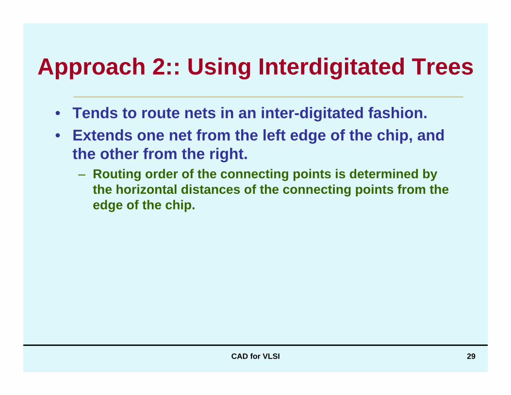
Approach 2:: Using Interdigitated Trees
• Tends to route nets in an inter-digitated fashion.• Extends one net from the left edge of the chip, and
the other from the right.– Routing order of the connecting points is determined by
the horizontal distances of the connecting points from the edge of the chip.

CAD for VLSI 30
Contd.
– Nets are determined by a combined Lee and Line Search algorithm.
• Points of the left net which lie in the left half of the chip are routed using a fast line search algorithm.
• Similarly, for the right net in the right half of the chip.• Next, all other points of the two sets are routed by Lee’s
algorithm.

CAD for VLSI 31

CAD for VLSI 32
Summary• Clock routing is one of the factors which determine the
throughput of any chip.• Power and ground routing needs special attention because of
wire widths.– Non-uniform wire widths.– Careful sizing of wires is required.
• Routing of power and ground nets is often given first priority.– Usually laid out entirely on metal layer(s).– Signal nets may share the metal layer(s) with power and ground,
but they change layers whenever a power or ground wire is encountered.
• Choice of layer:– Aluminium most widely used.– Superconductivity and optical interconnects for future high-
performance chips.
Over-The-Cell Routing
CAD for VLSI 34
Introduction
• Used in sophisticated channel routers in standard cell based designs.
• Basic idea:– Use of area outside the channel to obtain reduction in
channel height.– Routing over the cell rows is possible due to limited use of
the second and third metal layers.

CAD for VLSI 35
Basic Steps in OTC Routing
• Step 1: Net decomposition– Each multi-terminal net is partitioned into a set of 2-
terminal nets (defined based on x-coordinates of their left ends).
• Step 2: Net classification– Each net is classified into one of following types:
• Type 1: There is a vacant terminal directly opposite to one of the terminals of the net.
• Type 2: There is a vacant terminal between the two terminals of the net.
• Type 3: None of the above.

CAD for VLSI 36
Contd.
• Step 3: Vacant terminal assignment– Vacant terminals are assigned to each net depending on its
type and weight.– Weight of a net is defined as the improvement in channel
congestion possible if this net can be routed over the cell.• Step 4: Over-the-cell routing
– The selected nets are assigned exact geometric paths for routing in the area over the cells.
• Step 5: Channel segment assignment & routing– Selects the best net segments to be routed in the channel.– Route them using any available channel router.

CAD for VLSI 37
Example
Greedy channel router
OTC routing


![High-Speed Clock Routing - Purdue University · 2005. 8. 26. · Bottom-Up Clock Tree Synthesis • Matching-based clock routing[Kahng-Cong-Robins, DAC’91] – Recursively match](https://img.dokumen.tips/doc/110x75/607bba681efd36316e6a14fc/high-speed-clock-routing-purdue-university-2005-8-26-bottom-up-clock-tree.jpg)